ge 6252 basic electrical and electronicsengineering · pdf filege 6252 basic electrical and...
TRANSCRIPT

GE 6252 BASIC ELECTRICAL AND ELECTRONICSENGINEERING
SCE Page 1 of 226 DEPARTMENT OF
EEE
A Course Material on
GE 6252 BASIC ELECTRICAL AND ELECTRONICS ENGINEERING
By
Mrs. R.HEMALATHA
Mrs.K.UMARANI
Mr.S.VIJAY
Mr.R.GUNASEKARAN
ASSISTANT PROFESSOR
DEPARTMENT OF ELECTRICAL AND ELECTRONICS ENGINEERING
SASURIE COLLEGE OF ENGINEERING
VIJAYAMANGALAM – 638 056
GE 6252 BASIC ELECTRICAL AND ELECTRONICSENGINEERING
SCE Page 2 of 226 DEPARTMENT OF
EEE
QUALITY CERTIFICATE
This is to certify that the e-course material
Subject Code : GE 6252
Subject: Basic Electrical and Electronics Engineering
Class : I Year Mechanical
Being prepared by me and it meets the knowledge requirement of the university curriculum.
Signature of the Author
Name:
Designation:
This is to certify that the course material being prepared by Mrs. Hemalatha.R is of adequate
quality. She has referred more than five books among them minimum one is from abroad author.
Signature of HD
Name:
SEAL

GE 6252 BASIC ELECTRICAL AND ELECTRONICSENGINEERING
SCE Page 3 of 226 DEPARTMENT OF
EEE
CONTENTS
S.NO TOPIC PAGE NO.
UNIT I ELECTRICAL CIRCUITS & MEASUREMENTS
1.1 Basic definitions 7
1.2 DC circuits 8
1.3 Ohm’s Law 10
1.4 AC Circuits 11
1.5 Kirchoff’s Laws 12
1.6 Steady State Solution of DC Circuits 13
1.7 Simple problems using ohm’s law 14
1.8 Introduction to AC Circuits 18
1.9 Waveforms and RMS Value 18
1.10 Power and Power factor 18
1.11 Single Phase and Three Phase Balanced Circuits 19
1.12 Operating Principles of Moving Coil Ammeters and Voltmeters 36
1.13 Operating Principles of Moving Iron Instruments Ammeters and
Voltmeters 40
1.14 Dynamometer type Watt meters 43
1.15 Dynamometer type Energy meters 47
UNIT II ELECTRICAL MECHANICS
2.1 Construction, Principle of Operation of DC Generators 50
2.2 Basic Equations and Applications of DC Generators 56
2.3 Construction, Principle of Operation of DC Motor 65

GE 6252 BASIC ELECTRICAL AND ELECTRONICSENGINEERING
SCE Page 4 of 226 DEPARTMENT OF
EEE
2.4 Basic Equations and Applications of DC Motor 69
2.5 Construction, Principle of Operation of Single Phase Transformer 71
2.6 Basic Equations and Applications of Single Phase Transformer 74
2.7 Construction, Principle of Operation of Single phase induction
Motor 82
2.8 Types of Single phase induction Motor 85
UNIT III SEMICONDUCTOR DEVICES AND APPLICATIONS
3.1 Characteristics of PN Junction Diode 98
3.2 Zener Effect 99
3.3 Zener Diode and its Characteristics 99
3.4 Half wave Rectifiers 101
3.5 Full wave Rectifiers 103
3.6 Voltage Regulation 104
3.7 Bipolar Junction Transistor 104
3.8 CB Configurations and Characteristics 108
3.9 CE Configurations and Characteristics 111
3.10 CC Configurations and Characteristics 115
3.11 Elementary Treatment of Small Signal Amplifier 118
UNIT IV DIGITAL ELECTRONICS
4.1 Binary Number System 119
4.2 Logic Gates 130
4.3 Boolean algebra 136
4.4 Half and Full Adders 138

GE 6252 BASIC ELECTRICAL AND ELECTRONICSENGINEERING
SCE Page 5 of 226 DEPARTMENT OF
EEE
4.5 Flip- Flops 140
4.6 Registers and Counters 146
4.7 A/D and D/A Conversion 150
UNIT V FUNDAMENTALS OF COMMUNICATION ENGINEERING
5.1 Types of Signals Analog and Digital Signals 156
5.2 Modulation and Demodulation Principles of Amplitude. 158
5.3 Modulation and Demodulation Principles of Frequency
Modulations. 160
5.4 Block diagram of Radio 164
5.5 Block diagram of TV 170
5.6 Block diagram of Microwave 173
5.7 Block diagram of Satellite 175
5.8 Block diagram of Optical Fiber 176
GLOSSARY 177
QUESTION BANK 187
UNIVERSITY QUESTION PAPER 219

GE 6252 BASIC ELECTRICAL AND ELECTRONICSENGINEERING
SCE Page 6 of 226 DEPARTMENT OF
EEE
UNIT I ELECTRICAL CIRCUITS & MEASUREMENTS 12
Ohm’s Law – Kirchoff’s Laws – Steady State Solution of DC Circuits – Introduction to AC
Circuits – Waveforms and RMS Value – Power and Power factor – Single Phase and Three
Phase Balanced Circuits.
Operating Principles of Moving Coil and Moving Iron Instruments (Ammeters and Voltmeters),
Dynamometer type Watt meters and Energy meters.
UNIT II ELECTRICAL MECHANICS 12
Construction, Principle of Operation, Basic Equations and Applications of DC Generators, DC
Motors, Single Phase Transformer, single phase induction Motor.
UNIT III SEMICONDUCTOR DEVICES AND APPLICATIONS 12
Characteristics of PN Junction Diode – Zener Effect – Zener Diode and its Characteristics – Half
wave and Full wave Rectifiers – Voltage Regulation. Bipolar Junction Transistor – CB, CE, CC
Configurations and Characteristics – Elementary Treatment of Small Signal Amplifier.
UNIT IV DIGITAL ELECTRONICS 12
Binary Number System – Logic Gates – Boolean Algebra – Half and Full Adders – Flip- Flops –
Registers and Counters – A/D and D/A Conversion (single concepts)
UNIT V FUNDAMENTALS OF COMMUNICATION ENGINEERING 12
Types of Signals: Analog and Digital Signals – Modulation and Demodulation: Principles of
Amplitude and Frequency Modulations. Communication Systems: Radio, TV, Fax, Microwave,
Satellite and Optical Fibre (Block Diagram Approach only).
TOTAL: 60 PERIODS
TEXT BOOKS:
1. V.N. Mittle “Basic Electrical Engineering”,Tata McGraw Hill Edition, New Delhi, 1990.
2. R.S. Sedha, “Applied Electronics” S. Chand & Co., 2006.
REFERENCES:
1. Muthusubramanian R, Salivahanan S and Muraleedharan K A, “Basic Electrical, Electronics
and Computer Engineering”,Tata McGraw Hill, Second Edition, (2006).
2. Nagsarkar T K and Sukhija M S, “Basics of Electrical Engineering”, Oxford press (2005).
3. Mehta V K, “Principles of Electronics”, S.Chand & Company Ltd, (1994).
4. Mahmood Nahvi and Joseph A. Edminister, “Electric Circuits”, Schaum’ Outline Series,
McGraw Hill, (2002).
5. Premkumar N, “Basic Electrical Engineering”, Anuradha Publishers, (2003).

GE 6252 BASIC ELECTRICAL AND ELECTRONICSENGINEERING
SCE Page 7 of 226 DEPARTMENT OF
EEE
UNIT – I ELECTRIC CIRCUITS & MEASUREMENTS
Prerequisites
Solid, Liquid and gas particles called molecules. These molecules are made up of atoms
which can be further spilt into electrons, protons and neutrons. The electrons revolve around the
nucleus. The electrons presents in the outer most orbits experience a very weak force of
attraction for the obvious reason that according to coulomb’s law, the force between two charges
varies inversely with the square of the distance. These electrons are known as free electrons. The
movement of electrons are known as electric current
Introduction
1.1 Basic Definitions
Electric current:
The continuous flow of electrons constitutes electric current. It is denoted by ‘I’ and is measured
in amperes.
‘I’ is also given by I = coulomb / sec
Electric Potential:
The electric potential at any point in an electric field is defined as the work done in brining an
unit positive charge (Q) from infinity to that point against the electric field
‘V’ is given by V =
Resistance:
It is the property of a conductor by which it opposes the flow of current. It is denoted by R and
its unit is ohms (Ω)
Laws of resistance:
The resistance of a conductor
(i). Varies directly with its length (l)
(ii).Varies inversely with its cross sectional area (A)
(iii). Depends on the nature of the material
(iv). Depends on the temperature
R α L
And R α 1/A
R α L / A
R = ρ L / A
Where ρ is called specific resistance
Specific resistance:
It is defined as the resistance offered by unit cube of the material between its opposite faces. It is
denoted by ρ and its unit is ohm – meter
ρ = RA / L

GE 6252 BASIC ELECTRICAL AND ELECTRONICSENGINEERING
SCE Page 8 of 226 DEPARTMENT OF
EEE
Temperature effect on resistance:
In the case of pure metals the resistance increases with increases in temperature. In case of alloys
the increase in resistance with increases in temperature is relatively small and irregular. The
resistance of electrolytes and insulators decreases with increases in temperature
Temperature co-efficient of resistance
It is defined as the change in resistance per ohm per degree change in temperature from 0°C. If a
material has resistance of R0, R1, and R2 at temperature of 0°C, t1°C and t2°C respectively, then
R1 = R0 (1 + α0 t1)
R2 = R0 (1+ α0 t2)
=
R2 = R1
R2 = R1
R2 = R1 (1+α0(t2-t1))
αt =
1.2. DC Circuits:
Prerequisites:
A DC circuit (Direct Current circuit) is an electrical circuit that consists of any
combination of constant voltage sources, constant current sources, and resistors. In this case,
the circuit voltages and currents are constant, i.e., independent of time. More technically,
a DC circuit has no memory. That is, a particular circuit voltage or current does not depend
on the past value of any circuit voltage or current. This implies that the system of equations
that represent a DC circuit do not involve integrals or derivatives.
Introduction:
In electronics, it is common to refer to a circuit that is powered by a DC voltage source such
as a battery or the output of a DC power supply as a DC circuit even though what is meant is
that the circuit is DC powered.
If a capacitor and/or inductor is added to a DC circuit, the resulting circuit is not,

GE 6252 BASIC ELECTRICAL AND ELECTRONICSENGINEERING
SCE Page 9 of 226 DEPARTMENT OF
EEE
strictly speaking, a DC circuit. However, most such circuits have a DC solution. This solution
gives the circuit voltages and currents when the circuit is in DC steady state. More
technically, such a circuit is represented by a system of differential equations. The
solution to these equations usually contains a time varying or transient part as well as
constant or steady state part. It is this steady state part that is the DC solution. There are some
circuits that do not have a DC solution. Two simple examples are a constant current
source connected to a capacitor and a constant voltage source connected to an inductor.
Electro-magnetic force(E.M.F):
Electromotive Force is, the voltage produced by an electric battery or generator in
an electrical circuit or, more precisely, the energy supplied by a source of electric power
in driving a unit charge around the circuit. The unit is the volt. A difference in charge
between two points in a material can be created by an external energy source such as a
battery. This causes electrons to move so that there is an excess of electrons at one point and
a deficiency of electrons at a second point. This difference in charge is stored as electrical
potential energy known as emf. It is the emf that causes a current to flow through a circuit.
Voltage:
Voltage is electric potential energy per unit charge, measured in joules per
coulomb. It is often referred to as "electric potential", which then must be distinguished from
electric potential energy by noting that the "potential" is a "per-unit-charge" quantity. Like
mechanical potential energy, the zero of potential can be chosen at any point, so the difference
in voltage is the quantity which is physically meaningful. The difference in voltage measured
when moving from point A to point B is equal to the work which would have to be done, per
unit charge, against the electric field to move the charge from A to B.
Potential Difference:
A quantity related to the amount of energy needed to move an object from one place to
another against various types of forces. The term is most often used as an abbreviation of
"electrical potential difference", but it also occurs in many other branches of physics. Only
changes in potential or potential energy (not the absolute values) can be measured.
Electrical potential difference is the voltage between two points, or the voltage drop
transversely over an impedance (from one extremity to another). It is related to the energy
needed to move a unit of electrical charge from one point to the other against the electrostatic
field that is present. The unit of electrical potential difference is the volt (joule per coulomb).
Gravitational potential difference between two points on Earth is related to the energy needed to
move a unit mass from one point to the other against the Earth's gravitational field. The unit
of gravitational potential differences is joules per kilogram.
Electromagnetism: When current passes through a conductor, magnetic field will be generated around the

GE 6252 BASIC ELECTRICAL AND ELECTRONICSENGINEERING
SCE Page 10 of 226 DEPARTMENT OF
EEE
conductor and the conductor become a magnet. This phenomenon is called electromagnetism.
Since the magnet is produced electric current, it is called the electromagnet. An electromagnet is
a type of magnet in which the magnetic field is produced by a flow of electric current. The
magnetic field disappears when the current ceases. In short, when current flow through a
conductor, magnetic field will be generated. When the current ceases, the magnetic field
disappear.
Applications of Electromagnetism:
Electromagnetism has numerous applications in today's world of science and physics. The
very basic application of electromagnetism is in the use of motors. The motor has a switch that
continuously switches the polarity of the outside of motor. An electromagnet does the same
thing. We can change the direction by simply reversing the current. The inside of the motor
has an electromagnet, but the current is controlled in such a way that the outside magnet
repels it.
Another very useful application of electromagnetism is the "CAT scan machine." This
machine is usually used in hospitals to diagnose a disease. As we know that current is
present in our body and the stronger the current, the strong is the magnetic field. This
scanning technology is able to pick up the magnetic fields, and it can be easily identified
where there is a great amount of electrical activity inside the body
The work of the human brain is based on electromagnetism. Electrical impulses cause
the operations inside the brain and it has some magnetic field. When two magnetic fields cross
each other inside the brain, interference occurs which is not healthy for the brain.
Ohm’s Law: Ohm's law states that the current through a conductor between two points is directly
proportional to the potential difference or voltage across the two points, and inversely
proportional to the resistance between them. The mathematical equation that describes this
relationship is:
where I is the current through the resistance in units of amperes,
V is the potential difference measured across the resistance in units of volts,
and R is the resistance of the conductor in units of ohms.
More specifically, Ohm's law states that the R in this relation is constant,
independent of the current.
AC Circuits:
Prerequisites:
An alternating current (AC) is an electrical current, where the magnitude of the

GE 6252 BASIC ELECTRICAL AND ELECTRONICSENGINEERING
SCE Page 11 of 226 DEPARTMENT OF
EEE
current varies in a cyclical form, as opposed to direct current, where the polarity of the current
stays constant.
The usual waveform of an AC circuit is generally that of a sine wave, as this results in
the most efficient transmission of energy. However in certain applications different waveforms
are used, such as triangular or square waves
Introduction:
Used generically, AC refers to the form in which electricity is delivered to businesses
and residences. However, audio and radio signals carried on electrical wire are also examples
of alternating current. In these applications, an important goal is often the recovery of
information encoded (or modulated) onto the AC signal.
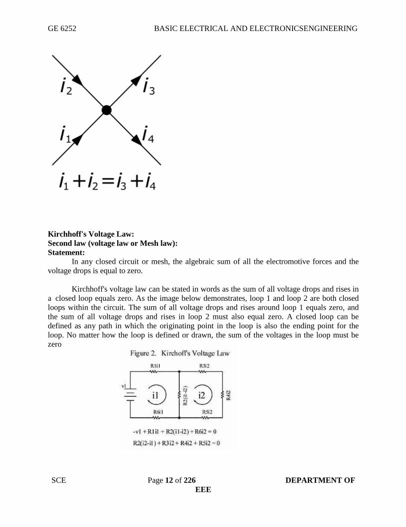
Kirchhoff’s law:
Kirchhoff's Current Law:
First law (Current law or Point law):
Statement:
The sum of the currents flowing towards any junction in an electric circuit equal to the sum of
currents flowing away from the junction.
Kirchhoff's Current law can be stated in words as the sum of all currents
flowing into a node is zero. Or conversely, the sum of all currents leaving a node must
be zero. As the image below demonstrates, the sum of currents Ib, Ic, and Id, must
equal the total current in Ia. Current flows through wires much like water flows
through pipes. If you have a definite amount of water entering a closed pipe system,
the amount of water that enters the system must equal the amount of water that
exists the system. The number of branching pipes does not change the net volume of
water (or current in our case) in the system.
GE 6252 BASIC ELECTRICAL AND ELECTRONICSENGINEERING
SCE Page 12 of 226 DEPARTMENT OF
EEE
Kirchhoff's Voltage Law:
Second law (voltage law or Mesh law):
Statement:
In any closed circuit or mesh, the algebraic sum of all the electromotive forces and the
voltage drops is equal to zero.
Kirchhoff's voltage law can be stated in words as the sum of all voltage drops and rises in
a closed loop equals zero. As the image below demonstrates, loop 1 and loop 2 are both closed
loops within the circuit. The sum of all voltage drops and rises around loop 1 equals zero, and
the sum of all voltage drops and rises in loop 2 must also equal zero. A closed loop can be
defined as any path in which the originating point in the loop is also the ending point for the
loop. No matter how the loop is defined or drawn, the sum of the voltages in the loop must be
zero

GE 6252 BASIC ELECTRICAL AND ELECTRONICSENGINEERING
SCE Page 13 of 226 DEPARTMENT OF
EEE
Steady State Solution of DC Circuits:
Resistance in series connection:
The resistors R1, R2, R3 are connected in series across the supply voltage “V”. The total current
flowing through the circuit is denoted as “I”. The voltage across the resistor R1, R2 and R3 is V1,
V2, and V3 respectively.
V1 = I*R1 (as per ohms law)
V2= I*R2
V3 = I*R3
V = V1+V2+V3
= IR1+IR2+IR3
= (R1+R2+R3) I
IR = (R1+R2+R3) I
R = R1+R2+R3
Resistance in parallel connection:
The resistors R1, R2, R3 are connected in parallel across the supply voltage “V”. The total
current flowing through the circuit is denoted as “I”. The current flowing through the resistor
R1, R2 and R3 is I1, I2, and I3 respectively.

GE 6252 BASIC ELECTRICAL AND ELECTRONICSENGINEERING
SCE Page 14 of 226 DEPARTMENT OF
EEE
I = V / R (as per ohms law)
I 1 = V1 / R1
I2 = V2 / R2
I3 = V3 / R3
V1 = V2 = V3 = V
From the above diagram
I = I1+I2+I3
= V1 / R1 + V2 / R2 + V3 / R3
= V / R1+ V/R2 +V/R3
I = V (1/R1 +1/R2 +1/R3)
V / R = V (1/R1 +1/R2 +1/R3)
1/R = 1/R1 +1/R2 +1/R3
Problems based on ohm’s law
Problem 1: A current of 0.5 A is flowing through the resistance of 10Ω.Find the potential difference
between its ends.
Given data:
Current I= 0.5A.
Resistance R=1Ω
To f ind
Potential difference V = ?
Formula used:
V = IR
Solution:
V = 0.5 × 10 = 5V.
Result :
The potential difference between its ends = 5 V
Problem :2
A supply voltage of 220V is applied to a 100 Ω resistor. Find the current flowing through
it.
Given data
Voltage V = 220V
Resistance R = 100Ω
To find:

GE 6252 BASIC ELECTRICAL AND ELECTRONICSENGINEERING
SCE Page 15 of 226 DEPARTMENT OF
EEE
Current I = ?
Formula used:
Current I = V / R
Solution:
Current I = 220/100
= 2.2 A
Result:
The current flowing through the resistor = 2.2 A
Problem : 3
Calculate the resistance of the conductor if a current of 2A flows through it when the
potential difference across its ends is 6V.
Given data
Current I = 2A
Voltage V = 6V
To find:
Resistance R = ?
Formula used:
Resistance R = V / I
Solution:
Resistance R = 6 / 2
= 3 Ω
Result:
The value of resistance R = 3Ω
Problem: 4
Calculate the current and resistance of a 100 W, 200V electric bulb.
Given data:
Power P = 100W
Voltage V = 200V
To find:
Current I =?
Resistance R =?
Formula used:
Power P = V *I
Current I = P / V
Resistance R = V / I

GE 6252 BASIC ELECTRICAL AND ELECTRONICSENGINEERING
SCE Page 16 of 226 DEPARTMENT OF
EEE
Solution:
Current I = P / V
= 100 / 200
= 0.5 A
Resistance R = V / I
= 200 / 0.2
= 400 Ω
Result:
The value of the current I = 0.5 A
The value of the Resistance R = 400 Ω
Problem: 5
A circuit is made of 0.4 Ω wire, a 150Ω bulb and a 120Ω rheostat connected in series. Determine
the total resistance of the circuit.
Given data:
Resistance of the wire = 0.4Ω
Resistance of bulb = 1 5 0 Ω
Resistance of rheostat = 120Ω
To find:
The total resistance of the circuit R T =?
Formula used:
The total resistance of the circuit R T = R1+R2+R3
Solution:
Total resistance ,R = 0.4 + 150 +120
= 270.4Ω
Result:
The total resistance of the circuit R T = 270.4 Ω
Problem 6:
Three resistances of values 2Ω, 3Ω and 5Ω are connected in series across 20 V, D.C supply
.Calculate (a) equivalent resistance of the circuit (b) the total current of the circuit (c) the voltage
drop across each resistor and (d) the power dissipated in each resistor.
Given data:
R1 = 2Ω
R2 = 3Ω
R3 = 5Ω
V = 20V

GE 6252 BASIC ELECTRICAL AND ELECTRONICSENGINEERING
SCE Page 17 of 226 DEPARTMENT OF
EEE
To find:
R T =?
I T =?
V1, V2, V3 =?
P1, P2, P3 =?
Formula used:
RT = R1+R2+R3 (series connection)
IT = VT / RT
V1 = R1*I1
V2= R2*I2
V3 = R3*I3
P1=V1*I1
P2=V2*I2
P3=V3*I3
Solution:
RT = R1+R2+R3
= 2+3+5
RT = 10Ω
IT = VT / RT
= 20 / 10
IT = 2 A
In series connection I1 = I2 = I3 = IT = 2A
V1 = I1*R1
= 2*2
V1 = 4 V
V2 = I2*R2
= 2*3
V2 = 6 V
V3 = I3*R3
= 5*2
V3 = 10V
P1 = V1*I1
= 4*2
P1 = 8W
P2 = V2*I2
= 6*2

GE 6252 BASIC ELECTRICAL AND ELECTRONICSENGINEERING
SCE Page 18 of 226 DEPARTMENT OF
EEE
P2 = 12W
P3 = V3*I3
= 10*2
P3 = 20W
Result:
(a). Equivalent resistance of the circuit RT = 10Ω
(b). The total current of the circuit IT = 2A
(c). Voltage drop across each resistor V1 = 4 V, V2 = 6 V, V3 = 10V
(d). The power dissipated in each resistor P1 = 8W, P2 = 12W, P3 = 20W
AC Instantaneous and RMS:
Instantaneous Value: The Instantaneous value of an alternating voltage or current is the value of voltage or
current at one particular instant. The value may be zero if the particular instant is the time in the
cycle at which the polarity of the voltage is changing. It may also be the same as the peak value,
if the selected instant is the time in the cycle at which the voltage or current stops increasing and
starts decreasing. There are actually an infinite number of instantaneous values between zero and
the peak value.
RMS Value: The average value of an AC waveform is NOT the same value as that for a DC waveforms
average value. This is because the AC waveform is constantly changing with time and the
heating effect given by the formula ( P = I 2.R ), will also be changing producing a positive
power consumption. The equivalent average value for an alternating current system that provides
the same power to the load as a DC equivalent circuit is called the "effective value". This
effective power in an alternating current system is therefore equal to: ( I2.R. Average).
As power is proportional to current squared, the effective current, I will be equal to √ I 2 Ave.
Therefore, the effective current in an AC system is called the Root Mean Squared or R.M.S.
Pure Resistive circuit:

GE 6252 BASIC ELECTRICAL AND ELECTRONICSENGINEERING
SCE Page 19 of 226 DEPARTMENT OF
EEE
Resistors are “passive” devices that are they do not produce or consume any electrical energy,
but convert electrical energy into heat. In DC circuits the linear ratio of voltage to current in a
resistor is called its resistance. However, in AC circuits this ratio of voltage to current depends
upon the frequency and phase difference or phase angle ( φ ) of the supply. So when using
resistors in AC circuits the term Impedance, symbol Z is the generally used and we can say that
DC resistance = AC impedance, R = Z.
It is important to note, that when used in AC circuits, a resistor will always have the same
resistive value no matter what the supply frequency from DC to very high frequencies, unlike
capacitor and inductors.
For resistors in AC circuits the direction of the current flowing through them has no effect on the
behaviour of the resistor so will rise and fall as the voltage rises and falls. The current and
voltage reach maximum, fall through zero and reach minimum at exactly the same time. i.e, they
rise and fall simultaneously and are said to be “in-phase” as shown below.
We can see that at any point along the horizontal axis that the instantaneous voltage and current
are in-phase because the current and the voltage reach their maximum values at the same time,
that is their phase angle θ is 0o. Then these instantaneous values of voltage and current can be
compared to give the ohmic value of the resistance simply by using ohms law. Consider below
the circuit consisting of an AC source and a resistor.
The instantaneous voltage across the resistor, VR is equal to the supply voltage, Vt and is given
as:
VR = Vmax sinωt
The instantaneous current flowing in the resistor will therefore be:
IR = VR / R
= Vmax sinωt / R
= I max sinωt
In purely resistive series AC circuits, all the voltage drops across the resistors can be added
together to find the total circuit voltage as all the voltages are in-phase with each other. Likewise,
in a purely resistive parallel AC circuit, all the individual branch currents can be added together
to find the total circuit current because all the branch currents are in-phase with each other.

GE 6252 BASIC ELECTRICAL AND ELECTRONICSENGINEERING
SCE Page 20 of 226 DEPARTMENT OF
EEE
Since for resistors in AC circuits the phase angle φ between the voltage and the current is zero,
then the power factor of the circuit is given as cos 0o = 1.0. The power in the circuit at any
instant in time can be found by multiplying the voltage and current at that instant.
Then the power (P), consumed by the circuit is given as P = Vrms Ι cos Φ in watt’s. But
since cos Φ = 1 in a purely resistive circuit, the power consumed is simply given as, P =
Vrms Ι the same as for Ohm’s Law.
This then gives us the “Power” waveform and which is shown below as a series of positive
pulses because when the voltage and current are both in their positive half of the cycle the
resultant power is positive. When the voltage and current are both negative, the product of the
two negative values gives a positive power pulse.
Then the power dissipated in a purely resistive load fed from an AC rms supply is the same as
that for a resistor connected to a DC supply and is given as:
P = V rms * I rms
= I 2 rms * R
= V 2 rms / R
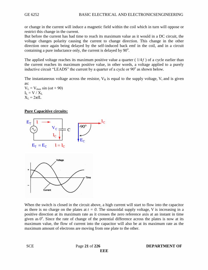
Pure Inductive circuits:
This simple circuit above consists of a pure inductance of L Henries ( H ), connected across a
sinusoidal voltage given by the expression: V(t) = Vmax sin ωt. When the switch is closed this
sinusoidal voltage will cause a current to flow and rise from zero to its maximum value. This rise
GE 6252 BASIC ELECTRICAL AND ELECTRONICSENGINEERING
SCE Page 21 of 226 DEPARTMENT OF
EEE
or change in the current will induce a magnetic field within the coil which in turn will oppose or
restrict this change in the current.
But before the current has had time to reach its maximum value as it would in a DC circuit, the
voltage changes polarity causing the current to change direction. This change in the other
direction once again being delayed by the self-induced back emf in the coil, and in a circuit
containing a pure inductance only, the current is delayed by 90o.
The applied voltage reaches its maximum positive value a quarter ( 1/4ƒ ) of a cycle earlier than
the current reaches its maximum positive value, in other words, a voltage applied to a purely
inductive circuit “LEADS” the current by a quarter of a cycle or 90o as shown below.
The instantaneous voltage across the resistor, VR is equal to the supply voltage, Vt and is given
as:
VL = Vmax sin (ωt + 90)
IL = V / XL
XL = 2πfL
Pure Capacitive circuits:
When the switch is closed in the circuit above, a high current will start to flow into the capacitor
as there is no charge on the plates at t = 0. The sinusoidal supply voltage, V is increasing in a
positive direction at its maximum rate as it crosses the zero reference axis at an instant in time
given as 0o. Since the rate of change of the potential difference across the plates is now at its
maximum value, the flow of current into the capacitor will also be at its maximum rate as the
maximum amount of electrons are moving from one plate to the other.

GE 6252 BASIC ELECTRICAL AND ELECTRONICSENGINEERING
SCE Page 22 of 226 DEPARTMENT OF
EEE
As the sinusoidal supply voltage reaches its 90o point on the waveform it begins to slow down
and for a very brief instant in time the potential difference across the plates is neither increasing
nor decreasing therefore the current decreases to zero as there is no rate of voltage change. At
this 90opoint the potential difference across the capacitor is at its maximum ( Vmax ), no current
flows into the capacitor as the capacitor is now fully charged and its plates saturated with
electrons.
At the end of this instant in time the supply voltage begins to decrease in a negative direction
down towards the zero reference line at 180o. Although the supply voltage is still positive in
nature the capacitor starts to discharge some of its excess electrons on its plates in an effort to
maintain a constant voltage. These results in the capacitor current flowing in the opposite or
negative direction.
When the supply voltage waveform crosses the zero reference axis point at instant 180o, the rate
of change or slope of the sinusoidal supply voltage is at its maximum but in a negative direction,
consequently the current flowing into the capacitor is also at its maximum rate at that instant.
Also at this 180o point the potential difference across the plates is zero as the amount of charge is
equally distributed between the two plates.
Then during this first half cycle 0o to 180
o, the applied voltage reaches its maximum positive
value a quarter (1/4ƒ) of a cycle after the current reaches its maximum positive value, in other
words, a voltage applied to a purely capacitive circuit “LAGS” the current by a quarter of a cycle
or 90o as shown below.
IC = Imax sin (ωt + 90)
IL = V / XC
XC = 1 / 2πfC
RL Series circuit:

GE 6252 BASIC ELECTRICAL AND ELECTRONICSENGINEERING
SCE Page 23 of 226 DEPARTMENT OF
EEE
In other words, an Inductor in an electrical circuit opposes the flow of current, ( i ) through it.
While this is perfectly correct, we made the assumption in the tutorial that it was an ideal
inductor which had no resistance or capacitance associated with its coil windings.
However, in the real world “ALL” coils whether they are chokes, solenoids, relays or any wound
component will always have a certain amount of resistance no matter how small associated with
the coils turns of wire being used to make it as the copper wire will have a resistive value.
Then for real world purposes we can consider our simple coil as being an “Inductance”, L in
series with a “Resistance”, R. In other words forming an LR Series Circuit.
A LR Series Circuit consists basically of an inductor of inductance L connected in series with a
resistor of resistance R. The resistance R is the DC resistive value of the wire turns or loops that
goes into making up the inductors coil
The above LR series circuit is connected across a constant voltage source, (the battery) and a
switch. Assume that the switch, S is open until it is closed at a time t = 0, and then remains
permanently closed producing a “step response” type voltage input. The current, i begins to flow
through the circuit but does not rise rapidly to its maximum value of Imax as determined by the
ratio of V / R(Ohms Law).
This limiting factor is due to the presence of the self induced emf within the inductor as a result
of the growth of magnetic flux, (Lenz’s Law). After a time the voltage source neutralizes the
effect of the self induced emf, the current flow becomes constant and the induced current and
field are reduced to zero.
We can use Kirchoffs Voltage Law, (KVL) to define the individual voltage drops that exist
around the circuit and then hopefully use it to give us an expression for the flow of current.
Vt = VR + VL
VR = I*R
VL = i dL / dt
V(t) = I*R + i dL / dt

GE 6252 BASIC ELECTRICAL AND ELECTRONICSENGINEERING
SCE Page 24 of 226 DEPARTMENT OF
EEE
Since the voltage drop across the resistor, VR is equal to IxR (Ohms Law), it will have the same
exponential growth and shape as the current. However, the voltage drop across the
inductor, VL will have a value equal to: Ve(-Rt/L)
. Then the voltage across the inductor, VL will
have an initial value equal to the battery voltage at time t = 0 or when the switch is first closed
and then decays exponentially to zero as represented in the above curves.
The time required for the current flowing in the LR series circuit to reach its maximum steady
state value is equivalent to about 5 time constants or 5τ. This time constant τ, is measured
by τ = L/R, in seconds, were R is the value of the resistor in ohms and L is the value of the
inductor in Henries. This then forms the basis of an RL charging circuit were 5τ can also be
thought of as “5 x L/R” or the transient time of the circuit.
The transient time of any inductive circuit is determined by the relationship between the
inductance and the resistance. For example, for a fixed value resistance the larger the inductance
the slower will be the transient time and therefore a longer time constant for the LR series circuit.
Likewise, for a fixed value inductance the smaller the resistance value the longer the transient
time.
However, for a fixed value inductance, by increasing the resistance value the transient time and
therefore the time constant of the circuit becomes shorter. This is because as the resistance
increases the circuit becomes more and more resistive as the value of the inductance becomes
negligible compared to the resistance. If the value of the resistance is increased sufficiently large
compared to the inductance the transient time would effectively be reduced to almost zero.
RC Series circuit:

GE 6252 BASIC ELECTRICAL AND ELECTRONICSENGINEERING
SCE Page 25 of 226 DEPARTMENT OF
EEE
The fundamental passive linear circuit elements are the resistor (R), capacitor (C)
and inductor (L). These circuit elements can be combined to form an electrical circuit in four
distinct ways: the RC circuit, the RL circuit, the LC circuit and the RLC circuit with the
abbreviations indicating which components are used. These circuits exhibit important types of
behaviour that are fundamental to analogue electronics. In particular, they are able to act
as passive filters. This article considers the RL circuit in both series and parallel as shown in the
diagrams.
In practice, however, capacitors (and RC circuits) are usually preferred to inductors since they
can be more easily manufactured and are generally physically smaller, particularly for higher
values of components.
Both RC and RL circuits form a single-pole filter. Depending on whether the reactive element (C
or L) is in series with the load, or parallel with the load will dictate whether the filter is low-pass
or high-pass.
Frequently RL circuits are used for DC power supplies to RF amplifiers, where the inductor is
used to pass DC bias current and block the RF getting back into the power supply.
RLC Series Circuit:

GE 6252 BASIC ELECTRICAL AND ELECTRONICSENGINEERING
SCE Page 26 of 226 DEPARTMENT OF
EEE
Difference between AC AND DC:
Current that f l o w s continuously in one direction is c a l l e d direct c u r r e n t .
Alternating current (A.C) is the current that flows in one direction for a brief time then
reverses and flows in opposite direction for a similar time. The source for alternating current is
called AC generator or alternator.
Cycle: One complete set of positive and negative values of an alternating quantity is called
cycle.
Frequency: The number of cycles made by an alternating quantity per second is called frequency. The
unit of frequency is Hertz(Hz)
Amplitude or Peak value The maximum positive or negative value of an alternating quantity is called amplitude or
peak value.
Average value: This is the average of instantaneous values of an alternating quantity over one complete
cycle of the wave.
Time period: The time taken to complete one complete cycle.
Star Delta transformation:
Star to Delta transformation:

GE 6252 BASIC ELECTRICAL AND ELECTRONICSENGINEERING
SCE Page 27 of 226 DEPARTMENT OF
EEE
Star Delta Transformations allow us to convert impedances connected together from one type
of connection to another. We can now solve simple series, parallel or bridge type resistive
networks using Kirchhoff´s Circuit Laws, mesh current analysis or nodal voltage analysis
techniques but in a balanced 3-phase circuit we can use different mathematical techniques to
simplify the analysis of the circuit and thereby reduce the amount of math’s involved which in
itself is a good thing.
Standard 3-phase circuits or networks take on two major forms with names that represent the
way in which the resistances are connected, a Star connected network which has the symbol of
the letter, Υ (wye) and a Delta connected network which has the symbol of a triangle, Δ (delta).
If a 3-phase, 3-wire supply or even a 3-phase load is connected in one type of configuration, it
can be easily transformed or changed it into an equivalent configuration of the other type by
using either the Star Delta Transformation or Delta Star Transformation process.
A resistive network consisting of three impedances can be connected together to form a T or
“Tee” configuration but the network can also be redrawn to form a Star or Υ type network as
shown below.
As we have already seen, we can redraw the T resistor network to produce an
equivalent Star or Υ type network. But we can also convert a Pi or π type resistor network into an
equivalent Delta or Δ type network as shown below.

GE 6252 BASIC ELECTRICAL AND ELECTRONICSENGINEERING
SCE Page 28 of 226 DEPARTMENT OF
EEE
Pi-connected and Equivalent Delta Network.
Having now defined exactly what is a Star and Delta connected network it is possible to
transform the Υ into an equivalent Δ circuit and also to convert a Δ into an equivalent Υ circuit
using a the transformation process. This process allows us to produce a mathematical
relationship between the various resistors giving us a Star Delta Transformation as well as
a Delta Star Transformation.
These Circuit Transformations allow us to change the three connected resistances (or
impedances) by their equivalents measured between the terminals 1-2, 1-3 or 2-3 for either a star
or delta connected circuit. However, the resulting networks are only equivalent for voltages and
currents external to the star or delta networks, as internally the voltages and currents are different
but each network will consume the same amount of power and have the same power factor to
each other.
The value of the resistor on any one side of the delta, Δ network is the sum of all the two-product
combinations of resistors in the star network divide by the star resistor located “directly
opposite” the delta resistor being found.
For example, resistor A is given as:
A= (PQ + QR + RP) / R with respect to terminal 3
and resistor B is given as:
B = (PQ + QR + RP) / Q with respect to terminal 2 and
resistor C given as:
B = (PQ + QR + RP) / R with respect to terminal 1.
By dividing out each equation by the value of the denominator we end up with three separate
transformation formulas that can be used to convert any Delta resistive network into an
equivalent star network as given below.
Star Delta Transformation allows us to convert one type of circuit connection into another type
in order for us to easily analyze the circuit and star delta transformation techniques can be used
for either resistances or impedances.
One final point about converting a star resistive network to an equivalent delta network. If all the
resistors in the star network are all equal in value then the resultant resistors in the equivalent
delta network will be three times the value of the star resistors and equal,
giving: RDELTA = 3RSTAR

GE 6252 BASIC ELECTRICAL AND ELECTRONICSENGINEERING
SCE Page 29 of 226 DEPARTMENT OF
EEE
Delta to Star Transformation
Compare the resistances between terminals 1 and 2.
P+Q= A in parallel with (B+C)
P+Q = A(B+C) / A+B+C……………….(1)
Resistance between the terminals 2 and 3.
Q+R = C in parallel with (A+B)
Q+R=C(A+B) / A+B+C……………….(2)
Resistance between the terminals 1 and 3.
P+R = B in parallel with (A+C)
P+R = B(A+C) / A+B+C………………(3)
This now gives us three equations and taking equation 3 from equation 2 gives:
P+R-Q-R = (B(A+C)) –( C(A+B) ) / A+B+C
P-Q =(BA + BC – CA – BC) / A+B+C
P-Q = BA – CA / (A+B+C)…………….(4)
Then, re-writing Equation 1 will give us:
P+Q = (AB+AC) / A+B+C …………………….(5)
Equ (4) + Equ (5)
P+Q+ P-Q = (AB+AC) / A+B+C + (BA – CA) / A+B+C
2P = (AB+AC+BA-CA) / A+B+C
2P = 2AB / A+B+C
P = AB / A+B+C
Then to summarize a little about the above maths, we can now say that resistor P in a Star
network can be found as Equation 1 plus (Equation 3 minus Equation 2) or Eq1 + (Eq3 – Eq2).
Similarly, to find resistor Q in a star network, is equation 2 plus the result of equation 1 minus
equation 3 or Eq2 + (Eq1 – Eq3) and this gives us the transformation of Q as:
Q = AC / A+B+C
and again, to find resistor R in a Star network, is equation 3 plus the result of equation 2 minus
equation 1 or Eq3 + (Eq2 – Eq1) and this gives us the transformation of R as:
R = BC / A+B+C

GE 6252 BASIC ELECTRICAL AND ELECTRONICSENGINEERING
SCE Page 30 of 226 DEPARTMENT OF
EEE
When converting a delta network into a star network the denominators of all of the
transformation formulas are the same: A + B + C, and which is the sum of ALL the delta
resistances. Then to convert any delta connected network to an equivalent star network
If the three resistors in the delta network are all equal in value then the resultant resistors in the
equivalent star network will be equal to one third the value of the delta resistors, giving each
branch in the star network as: RSTAR = 1/3RDELTA
Measuring Instruments:
Classification of instruments
(i). Depending on the quality measured
(ii). Depending on the different principles used for their working
(iii). Depending on how the quantity is measured
Depending on the quality measured
Voltmeter
Ammeter
Energy meter
Ohm meter
Depending on the different principles used for their working
Moving Iron type
Moving coil type
Dynamometer type
Induction type
Depending on how the quantity is measured
Deflecting type
Integrating type
Recording type
Deflecting Torque
The deflecting torque moves the moving system and the pointer from the zero position. The
deflecting torque can be obtained through magnetic, thermal, electromagnetic or electro dynamic
effects
Controlling torque
The controlling torque acts in a direction opposite to that of deflecting torque. When the
controlling torque (TC) and the deflecting torque (TD) are numerically equal the pointer takes a
definite position. In the absence of TC the pointer would deflect to maximum position
irrespective of the quantity to be measured. Moreover TC also helps in bringing the moving
system to zero position when the instrument is disconnected from the circuit. The controlling
torque is obtained through spring control and gravity control
Spring Control:

GE 6252 BASIC ELECTRICAL AND ELECTRONICSENGINEERING
SCE Page 31 of 226 DEPARTMENT OF
EEE
The arrangement for spring control consists of two phosphor bronze spiral hair springs attached
to a moving system. The springs are made of materials which (i). are not affected by fatigue. (ii).
Have low temp-coefficient of resistance (iii). Have low specific resistance (iv). Are non-
magnetic
As the pointer deflects the springs get twisted in the opposite direction. The combined twist
produces the necessary controlling torque which is proportional to angle of deflection of moving
system θ. If we consider a permanent magnet moving coil meter with spring control system the
deflecting torque will be proportional to the current passing through it and the controlling torque
will be proportional to the angle of deflection
Thus TD α I
TC α θ
Since TD = TC
We have θ α I
Thus the spring controlled instruments having uniform scale
Gravity control

GE 6252 BASIC ELECTRICAL AND ELECTRONICSENGINEERING
SCE Page 32 of 226 DEPARTMENT OF
EEE
In gravity controlled instruments, as shown in Fig. 12.2 (a) a small adjustable weight is attached
to the spindle of the moving system such that the deflecting torque produced by the instrument
has to act against the action of gravity. Thus a controlling torque is obtained. This weight is
called the control weight. Another adjustable weight is also attached is the moving system for
zero adjustment and balancing purpose. This weight is called Balance weight.
When the control weight is in vertical position as shown in Fig. 12.2 (a), the controlling torque is
zero and hence the pointer must read zero. However, if the deflecting torque lifts the controlling
weight from position A to B as shown in Fig.12.2 (b) such that the spindle rotates by an angle θ,
then due to gravity a restoring (or controlling) torque is exterted on the moving system.
The controlling (or restoring) torque, Tc , is given by
Tc = Wl sin θ = k g sin θ
where W is the control weight;
l is the distance of the control weight from the axis of rotation of the moving system;
and k g is the gravity constant.
Equation shows the controlling torque can be varied quite simply by adjustment of the position
of the control weight upon the arm which carries it. Again, if the deflecting torque is directly
proportional to the current,
i.e., Td = kI
We have at the equilibrium position
Td = Tc
kI = k g sin θ
I = g k sin θ / k
This relation shows that current I is proportional to sin θ and not θ. Hence in gravity controlled
instruments the scale is not uniform. It is cramped for the lower readings, instead of being
uniformly divided, for the deflecting torque assumed to be directly proportional to the quantity
being measured.
Advantanges of Gravity Control
1. It is cheap and not affected by temperature variations.
2. It does not deteriorate with time.

GE 6252 BASIC ELECTRICAL AND ELECTRONICSENGINEERING
SCE Page 33 of 226 DEPARTMENT OF
EEE
3. It is not subject to fatigue.
Disadvantages of Gravity Control
1. Since the controlling torque is proportional to the sine of the angle of deflection, the scale is
not uniformly divided but cramped at its lower end.
2. It is not suitable for use in portable instruments (in which spring control is always preferred).
3. Gravity control instruments must be used in vertical position so that the control weight may
operate and also must be leveled otherwise they will give zero error. In view of these reasons,
gravity control is not used for indicating instruments in general and portable instruments in
particular.
Damping Torque
We have already seen that the moving system of the instrument will tend to move under the
action of the deflecting torque. But on account of the control torque, it will try to occupy a
position of rest when the two torques are equal and opposite. However, due to inertia of the
moving system, the pointer will not come to rest immediately but oscillate about its final
deflected position as shown in Fig and takes appreciable time to come to steady state. To
overcome this difficulty a damping torque is to be developed by using a damping device attached
to the moving system.
The damping torque is proportional to the speed of rotation of the moving system,
that is Tv = kv d dt θ
where kv = damping torque constant
d dt θ = speed of rotation of the moving system
Depending upon the degree of damping introduced in the moving system, the instrument may
have any one of the following conditions as depicted in Fig.
1. Under damped condition: The response is oscillatory
2. Over damped condition: The response is sluggish and it rises very slowly from its zero
position to final position.
3. Critically damped condition: When the response settles quickly without any oscillation, the
system is said to be critically damped.

GE 6252 BASIC ELECTRICAL AND ELECTRONICSENGINEERING
SCE Page 34 of 226 DEPARTMENT OF
EEE
In practice, the best response is slightly obtained when the damping is below the critical value
i.e., the instrument is slightly under damped.
The damping torque is produced by the following methods: Air Friction Damping & Fluid
friction damping
Air Friction Damping
In this type of damping a light vane or vanes having considerable area is attached to the moving
system to develop a frictional force opposing the motion by reason of the air they displace. Two
methods of damping by air friction are depicted in Fig.
The arrangement shown in Fig consists of a light aluminum vane which moves in a quadrant
(sector) shaped air chamber. The chamber also carries a cover plate at the top. The vane is
mounted on the spindle of the moving system. The aluminum vane should not touch the air-
chamber walls otherwise a serious error in the deflection of the instrument will be introduced.
Now, with the motion, the vane displaces air and thereby a damping force is created on the vane
that produces a torque (damping) on the spindle. When the movement is quicker the damping
force is greater; when the spindle is at rest, the damping force is zero.
The arrangement of Fig. consists of a light aluminum piston which is attached to the moving
system. This piston moves in a fixed chamber which is closed at one end. Either circular or
rectangular chamber may be used. The clearance (or gap) between the piston and chamber walls
should be uniform throughout and as small as possible. When the piston moves rapidly into the
chamber the air in the closed space is compressed and the pressure of air thus developed opposes
the motion of the piston and thereby the whole moving system. If the piston is moving out of the
chamber, rapidly, the pressure in the closed space falls and the pressure on the open side of the
piston is greater than that on the opposite side. Motion is thus again opposed. With this damping
system care must be taken to ensure that the arm carrying the piston should not touch the sides of
the chamber during its movement. The friction which otherwise would occur may introduce a
serious error in the deflection.
The air friction damping is very simple and cheap. But care must be taken to ensure that the
piston is not bent or twisted. This method is used in moving iron and hot wire instruments.
Fluid Friction Damping

GE 6252 BASIC ELECTRICAL AND ELECTRONICSENGINEERING
SCE Page 35 of 226 DEPARTMENT OF
EEE
This form is damping is similar to air friction damping. The action is the same as in the air
friction damping. Mineral oil is used in place of air and as the viscosity of oil is greater, the
damping force is also much greater. The vane attached to the spindle is arranged to move in the
damping oil. It is rarely used in commercial type instruments. The oil used must fulfill the
following requirements. It should not evaporate quickly . It should not have any corrosive effect
on metals. Its viscosity should not change appreciably with temperature. It should be good
insulator.
Advantages of Fluid Friction Damping
1. The oil used for damping can also be used for insulation purpose in some forms of instruments
which are submerged in oil.
2. The clearance between the vanes and oil chamber is not as critical as with the air friction
clamping system.
3. This method is suitable for use with instruments such as electrostatic type where the
movement is suspended rather than pivoted.
4. Due to the up thrust of oil, the loads on bearings or suspension system is reduced thereby the
reducing the frictional errors.
Disadvantages of Fluid Friction Damping
1. The instruments with this type of damping must be kept always in a vertical position.
2. It is difficult to keep the instrument clean due to leakage of oil.
3. It is not suitable for portable instruments. The fluid friction damping can be used for
laboratory type electrostatic instruments.
Eddy current damping
Eddy Current Damping

GE 6252 BASIC ELECTRICAL AND ELECTRONICSENGINEERING
SCE Page 36 of 226 DEPARTMENT OF
EEE
Eddy current damping is the most efficient form of damping. The essential components in this
type of damping are a permanent magnet; and a light conducting disc usually of alumninum.
When a sheet of conducting material moves in a magnetic field so as to cut through lines of
force, eddy currents are set up in it and a force exists between these currents and the magnetic
field, which is always in the direction opposing the motion. \
This force is proportional to the magnitude of the current, and to the strength of field. The former
is proportional to the velocity of movement of the conductor, and thus, if the magnetic field is
constant, the damping force is proportional to the velocity of the moving system and is zero
when there is no movement of the system.
PMMC

GE 6252 BASIC ELECTRICAL AND ELECTRONICSENGINEERING
SCE Page 37 of 226 DEPARTMENT OF
EEE
The permanent magnet moving coil instrument or PMMC type instrument uses two permanent
magnets in order to create stationary magnetic field. These types of instruments are only used for
measuring the dc quantities as if we apply ac current to these type of instruments the direction
of current will be reversed during negative half cycle and hence the direction of torque will also
be reversed which gives average value of torque zero. The pointer will not deflect due to high
frequency from its mean position showing zero reading. However it can measure the
direct current very accurately.
Construction of permanent magnet moving coil instruments.
We will see the construction of these types of instruments in four parts and they are described
below:
Stationary part or magnet system: In the present time we use magnets of high field intensities,
high coercive force instead of using U shaped permanent magnet having soft iron pole pieces.
The magnets which we are using nowadays are made up of materials like alcomax and alnico
which provide high field strength.
Moving coil: The moving coil can freely moves between the two permanent magnets as shown
in the figure given below. The coil is wound with many turns of copper wire and is placed on
rectangular aluminum which is pivoted on jeweled bearings.
Control system: The spring generally acts as control system for PMMC instruments. The spring
also serves another important function by providing the path to lead current in and out of the coil.
Damping system: The damping force hence torque is provided by movement of aluminium
former in the magnetic field created by the permanent magnets.
Meter: Meter of these instruments consists of light weight pointer to have free movement and
scale which is linear or uniform and varies with angle
Deflecting torque Equation:
Let us derive a general expression for torque in permanent magnet moving coil instruments
or PMMC instruments. We know that in moving coil instruments the deflecting torque is given

GE 6252 BASIC ELECTRICAL AND ELECTRONICSENGINEERING
SCE Page 38 of 226 DEPARTMENT OF
EEE
by the expression:
Td = N B l dI
where N is number of turns,
B is magnetic flux density in air gap,
l is the length of moving coil,
d is the width of the moving coil,
And I is the electric current.
Now for a moving coil instruments deflecting torque should be proportional to current,
mathematically we can write Td = GI.
Thus on comparing we say G = NBIdl.
At steady state we have both the controlling and deflecting torques are equal.
Tc is controlling torque, on equating controlling torque with deflection torque we have
GI = K.x where x is deflection thus current is given by
I = K / G x
Since the deflection is directly proportional to the current therefore we need a uniform scale on
the meter for measurement of current.
Now we are going to discuss about the basic circuit diagram of the ammeter. Let us consider a
circuit as shown below:
The current I is shown which breaks into two components at the point A. The two components
are Is and Im. Before I comment on the magnitude values of these currents, let us know more
about the construction of shunt resistance. The basic properties of shuntresistance are written
below,
The electrical resistance of these shunts should not differ at higher temperature, it they should

GE 6252 BASIC ELECTRICAL AND ELECTRONICSENGINEERING
SCE Page 39 of 226 DEPARTMENT OF
EEE
posses very low value of temperature coefficient. Also the resistance should be time
independent. Last and the most important property they should posses is that they should be able
to carry high value of current without much rise in temperature. Usually manganin is used for
making dc resistance. Thus we can say that the value of Is much greater than the value of Im as
resistance of shunt is low. From the we have,
Is .Rs = ImRm
Where Rs is resistance of shunt and Rm is the electrical resistance of the coil.
Is = I – Im
M= I / Im = 1+ (Rm + Rs)
Where m is the magnifying power of the shunt.
Errors in Permanent Magnet Moving Coil Instruments
There are three main types of errors
(a) Errors due to permanent magnets:
Due to temperature effects and aging of the magnets the magnet may lose their magnetism to
some extent. The magnets are generally aged by the heat and vibration treatment.
(b) Error may appear in PMMC Instrument due to the aging of the spring.
However the error caused by the aging of the spring and the errors caused due to permanent
magnet are opposite to each other, hence both the errors are compensated with each other.
(c) Change in the resistance of the moving coil with the temperature: Generally the temperature coefficients of the value of coefficient of copper wire in moving coil
is 0.04 per degree Celsius rise in temperature. Due to lower value of temperature coefficient the
temperature rises at faster rate and hence the resistance increases. Due to this significant amount
of error is caused.
Advantages of Permanent Magnet Moving Coil Instruments
(1)The scale is uniformly divided as the current is directly proportional to deflection of the
pointer. Hence it is very easy to measure quantities from these instruments.
(2)Power consumption is also very low in these types of instruments.
(3)Higher value of torque is to weight ratio.
(4)These are having multiple advantages, a single instrument can be used for measuring various
quantities by using different values of shunts and multipliers.
Disadvantages of Permanent Magnet Moving Coil Instruments
(1) These instruments cannot measure ac quantities.
(2) Cost of these instruments is high as compared to moving iron instruments
GE 6252 BASIC ELECTRICAL AND ELECTRONICSENGINEERING
SCE Page 40 of 226 DEPARTMENT OF
EEE
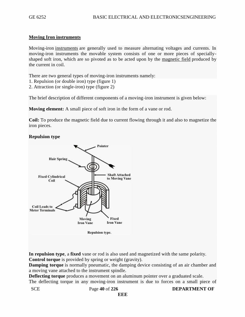
Moving Iron instruments
Moving-iron instruments are generally used to measure alternating voltages and currents. In
moving-iron instruments the movable system consists of one or more pieces of specially-
shaped soft iron, which are so pivoted as to be acted upon by the magnetic field produced by
the current in coil.
There are two general types of moving-iron instruments namely:
1. Repulsion (or double iron) type (figure 1)
2. Attraction (or single-iron) type (figure 2)
The brief description of different components of a moving-iron instrument is given below:
Moving element: A small piece of soft iron in the form of a vane or rod.
Coil: To produce the magnetic field due to current flowing through it and also to magnetize the
iron pieces.
Repulsion type
In repulsion type, a fixed vane or rod is also used and magnetized with the same polarity.
Control torque is provided by spring or weight (gravity).
Damping torque is normally pneumatic, the damping device consisting of an air chamber and
a moving vane attached to the instrument spindle.
Deflecting torque produces a movement on an aluminum pointer over a graduated scale.
The deflecting torque in any moving-iron instrument is due to forces on a small piece of

GE 6252 BASIC ELECTRICAL AND ELECTRONICSENGINEERING
SCE Page 41 of 226 DEPARTMENT OF
EEE
magnetically ‘soft’ iron that is magnetized by a coil carrying theoperating current. In repulsion
type moving–iron instrument consists of two cylindrical soft iron vanes mounted within a fixed
current-carrying coil. One iron vane is held fixed to the coil frame and other is free to rotate,
carrying with it the pointer shaft. Two irons lie in the magnetic field produced by the coil that
consists of only few turns if the instrument is an ammeter or of many turns if the instrument is
a voltmeter.
Current in the coil induces both vanes to become magnetized and repulsion between the
similarly magnetized vanes produces a proportional rotation. The deflecting torque is
proportional to the square of the current in the coil, making the instrument reading is a true
‘RMS’ quantity Rotation is opposed by a hairspring that produces the restoring torque . Only
the fixed coil carries load current, and it is constructed so as to withstand high transient
current.
Moving iron instruments having scales that are nonlinear and somewhat crowded in the lower
range of calibration.
Measurement of Electric Voltage and Current
Moving iron instruments are used as Voltmeter and Ammeter only.
Both can work on AC as well as on DC.
Ammeter Instrument used to measure current in the circuit.
Always connected in series with the circuit and carries the current to be measured.
This current flowing through the coil produces the desired deflecting torque.
It should have low resistance as it is to be connected in series.
Voltmeter
Instrument used to measure voltage between two points in a circuit.
Always connected in parallel.

GE 6252 BASIC ELECTRICAL AND ELECTRONICSENGINEERING
SCE Page 42 of 226 DEPARTMENT OF
EEE
Current flowing through the operating coil of the meter produces deflecting torque.
It should have high resistance. Thus a high resistance of order of kilo ohms is connected in
series with the coil of the instrument.
Ranges of Ammeter and Voltmeter
For a given moving-iron instrument the ampere-turns necessary to produce full-scale deflection
are constant.
One can alter the range of ammeters by providing a shunt coil with the moving coil.
Voltmeter range may be altered connecting a resistance in series with the coil. Hence the same
coil winding specification may be employed for a number of ranges.
Advantages
1. The instruments are suitable for use in AC and DC circuits.
2. The instruments are robust, owing to the simple construction of the moving parts.
3. The stationary parts of the instruments are also simple.
4. Instrument is low cost compared to moving coil instrument.
5. Torque/weight ratio is high, thus less frictional error.
Errors
(i). Error due to variation in temperature.
(ii). Error due to friction is quite small as torque-weight ratio is high in moving coil
instruments.
(iii). Stray fields cause relatively low values of magnetizing force produced by the coil.
Efficient magnetic screening is essential to reduce this effect.
(iv). Error due to variation of frequency causes change of reactance of the coil and also
changes the eddy currents induced in neighbouring metal.
(v). Deflecting torque is not exactly proportional to the square of the current due to non-linear
characteristics of iron material.
Attraction type

GE 6252 BASIC ELECTRICAL AND ELECTRONICSENGINEERING
SCE Page 43 of 226 DEPARTMENT OF
EEE
The basic construction of attraction type moving iron instrument is illustrated bellow
A thin disc of soft iron is eccentrically pivoted in front of a coil. This iron tends to move inward
that is from weaker magnetic field to stronger magnetic field whencurrent flowing through the
coil. In attraction moving instrument gravity control was used previously but now gravity control
method is replaced by spring control in relatively modern instrument. By adjusting balance
weight null deflection of the pointer is achieved. The required damping force is provided in this
instrument by air friction. The figure shows a typical type of damping system provided in the
instrument, where damping is achieved by a moving piston in an air syringe.
Theory of Attraction Type Moving Iron Instrument
Suppose when there is no current through the coil, the pointer is at zero, the angle made by the
axis of the iron disc with the line perpendicular to the field is φ. Now due current I and
corresponding magnetic field strength, the iron piece is deflected to an angle θ. Now component
of H in the direction of defected iron disc axis is Hcos90 - (θ + φ) or Hsin(θ + φ). Now force F
acting on the disc inward to the coil is thus proportional to H2sin(θ + φ) hence the force is also
proportional to I2sin(θ + φ) for constant permeability. If this force is acting on the disc at a
distance l from the pivot, then deflection torque,
Td = Fl cos (θ+Φ)
Thus Td = I2 sin (θ+Φ) cos (θ+Φ)
Td = kI2 sin 2(θ+Φ)
Where k is constant.
Now, as the instrument is gravity controlled, controlling torque will be
Tc = k’ sin θ
Where k ‘is constant
Dynamo meter type watt meter
In general, a watt meter is used to measure the electric power of a circuit, or sometime it also
measures the rate of energy transferred from one circuit to another circuit. When a moving coil
(that is free to rotate) is kept under the influence of a current carrying conductor, then
automatically a mechanical force will be applied to the moving coil, and this force will make a
little deflection of the moving coil. If a pointer is connected with the moving coil, which will
move of a scale, then the deflection can be easily measured by connecting the moving coil with
that pointer. This is the principle of operation of all dynamo meter type instruments, and this
principle is equally applicable for dynamo meter type watt meter also.
This type of watt meter consists of two types of coil, more specifically current coil and voltage
coil. There are two current coils which are kept at constant position and the measurable current
will flow through those current coils. A voltage coil is placed inside those two current coils, and
this voltage coil is totally free to rotate. The current coils are arranged such a way, that they are
connected with the circuit in series. And the voltage coil is connected in parallel with the circuit.

GE 6252 BASIC ELECTRICAL AND ELECTRONICSENGINEERING
SCE Page 44 of 226 DEPARTMENT OF
EEE
As simple as other voltmeter and ammeter connection. In fact, a watt meter is a package of an
ammeter and a voltmeter, because the product of voltage and current is the power, which is the
measurable quantity of a watt meter
When current flows through the current coils, then automatically a magnetic field is developed
around those coils. Under the influence of the electromagnetic field, voltage coil also carries
some amount of current as it is connected with the circuit in parallel. In this way, the deflection
of the pointer will proportional to both current and voltage of the circuit. In this way, Watt =
Current × Voltage equation is satisfied and the deflection shows the value of power inside the
circuit. A dynamo meter type watt meter is used in various applications where the power or
energy transfer has to be measured.
Construction and Working Principle of Electrodynamometer Type Wattmeter
Now let us look at constructional details of electrodynamometer. It consists of following parts
There are two types of coils present in the electrodynamometer.
They are :
(a) Moving coil : Moving coil moves the pointer with the help of spring control instrument. A
limited amount of current flows through the moving coil so as to avoid heating. So in order to
limit the current we have connect the high value resistor in series with the moving coil. The
moving is air cored and is mounted on a pivoted spindle and can moves freely.
In electrodynamometer type wattmeter, moving coil works as pressure coil. Hence moving
coil is connected across the voltage and thus the current flowing through this coil is always
proportional to the voltage.
(b) Fixed coil: The fixed coil is divided into two equal parts and these are connected in series
with the load, therefore the load current will flow through these coils. Now the reason is very
obvious of using two fixed coils instead of one, so that it can be constructed to carry considerable
amount of electric current. These coils are called the current coils of electrodynamometer type
wattmeter. Earlier these fixed coils are designed to carry the current of about 100 amperes but

GE 6252 BASIC ELECTRICAL AND ELECTRONICSENGINEERING
SCE Page 45 of 226 DEPARTMENT OF
EEE
now the modern wattmeter are designed to carry current of about 20 amperes in order to save
power.
(c) Control system: Out of two controlling systems i.e.
(1). Gravity control
(2) Spring control, only spring controlled systems are used in these types of wattmeter. Gravity
controlled system cannot be employed because they will appreciable amount of errors.
(d) Damping system: Air friction damping is used, as eddy current damping will distort the
weak operating magnetic field and thus it may leads to error.
(e) Scale: There is uniform scale is used in these types of instrument as moving coil moves
linearly over a range of 40 degrees to 50 degrees on either sides.
Now let us derive the expressions for the controlling torque and deflecting torques. In order to
derive these expressions let us consider the circuit diagram given below:
We know that instantaneous torque in electro dynamic type instruments is directly proportional
to product of instantaneous values of currents flowing through both the coils and the rate of
change of flux linked with the circuit.
Let I1 and I2 be the instantaneous values of currents in pressure and current coils respectively. So
the expression for the torque can be written as:
T = I1*I2*(dM / dx)
Where x is the angle
Now let the applied value of voltage across the pressure coil be V= V sin ωt
Assuming the electrical resistance of the pressure coil be very high hence we can neglect
reactance with respect to its resistance. In this the impedance is equal to its electrical
resistance therefore it is purely resistive
The expression for instantaneous current can be written as I2 = v / Rp where Rp is the
resistance of pressure coil.
I2 = V sin ωt / Rp

GE 6252 BASIC ELECTRICAL AND ELECTRONICSENGINEERING
SCE Page 46 of 226 DEPARTMENT OF
EEE
If there is phase difference between voltage and electric current, then expression for
instantaneous current through current coil can be written as
I1 = I(t) = I sin (ωt – Φ)
As current through the pressure coil in very very small compare to current through currentcoil
hence current through the current coil can be considered as equal to total load current.
Hence the instantaneous value of torque can be written as V sin ωt / Rp * I sin (ωt – Φ) *
(dM / dx)
Average value of deflecting torque can be obtained by integrating the instantaneous torque from
limit 0 to T where T is the time period of the cycle Td = deflecting torque = VI cosΦ /Rp *(dM /
dx)
Controlling torque is given by Tc = Kx where K is spring constant and x is final steady state value
of deflection.
Advantages of Electrodynamometer Type Wattmeter
Following are the advantages of electrodynamometer type wattmeters and they are written as
follows:
(a). Scale is uniform up to certain limit
(b). They can be used for both to measure AC as well as DC quantities as scale is calibrated for
both
Errors in Electrodynamometer Type Wattmeter
Following are the errors in the electrodynamometer type watt meters:
(a) Errors in the pressure coil inductance.
(b) Errors may be due to pressure coil capacitance.
(c) Errors may be due to mutual inductance effects.
(d) Errors may be due connections.(i.e. pressure coil is connected after current coil)
(e) Error due to Eddy currents.
(f) Errors caused by vibration of moving system.
(g) Temperature error.
(h) Errors due to stray magnetic field.

GE 6252 BASIC ELECTRICAL AND ELECTRONICSENGINEERING
SCE Page 47 of 226 DEPARTMENT OF
EEE
Single phase Energy meter
Single phase induction type energy meter is also popularly known as watt-hour meter. This
name is given to it. This article is only focused about its constructional features and its
working. Induction type energy meter essentially consists of following components:
1. Driving system
2. Moving system
3. Braking system and
4. Registering system
Driving system
It consists of two electromagnets, called “shunt” magnet and “series” magnet, of laminated
construction. A coil having large number of turns of fine wire is wound on the middle limb of
the shunt magnet.
This coil is known as “pressure or voltage” coil and is connected across the supply mains.
This voltage coil has many turns and is arranged to be as highly inductive as possible. In other
words, the voltage coil produces a high ratio of inductance to resistance. This causes the
current and therefore the flux, to lag the supply voltage by nearly 90 degree
Adjustable copper shading rings are provided on the central limb of the shunt magnet to make
the phase angle displacement between magnetic field set up by shunt magnet and supply
voltage is approximately 90 degree.
The copper shading bands are also called the power factor compensator or compensating loop.
The series electromagnet is energized by a coil, known as “current” coil which is connected in
series with the load so that it carry the load current. The flux produced by this magnet is
proportional to, and in phase with the load current.

GE 6252 BASIC ELECTRICAL AND ELECTRONICSENGINEERING
SCE Page 48 of 226 DEPARTMENT OF
EEE
Moving system
The moving system essentially consists of a light rotating aluminium disk mounted on a
vertical spindle or shaft. The shaft that supports the aluminium disk is connected by a gear
arrangement to the clock mechanism on the front of the meter to provide information that
consumed energy by the load.
The time varying (sinusoidal) fluxes produced by shunt and series magnet induce eddy
currents in the aluminium disc The interaction between these two magnetic fields and eddy
currents set up a driving torque in the disc. The number of rotations of the disk is therefore
proportional to the energy consumed by the load in a certain time interval and is commonly
measured in kilowatt-hours (Kwh).
Braking system
Damping of the disk is provided by a small permanent magnet, located diametrically
opposite to the a.c magnets. The disk passes between the magnet gaps. The movement of
rotating disc through the magnetic field crossing the air gap sets up eddy currents in the disc
that reacts with the magnetic field and exerts a braking torque.
By changing the position of the brake magnet or diverting some of the flux there form, the
speed of the rotating disc can be controlled.
Registering or counting system
.
The registering or counting system essentially consists of gear train, driven either by worm or
pinion gear on the disc shaft, which turns pointers that indicate on dials the number of times
the disc has turned.
The energy meter thus determines and adds together or integrates all the instantaneous power
values so that total energy used over a period is thus known. Therefore, this type of meter is
also called an “integrating” meter.

GE 6252 BASIC ELECTRICAL AND ELECTRONICSENGINEERING
SCE Page 49 of 226 DEPARTMENT OF
EEE
Working of Single phase induction type Energy Meter
The basic working of Single phase induction type Energy Meter is only focused on two
mechanisms:
1. Mechanism of rotation of an aluminum disc which is made to rotate at a speed proportional to
the power.
2. Mechanism of counting and displaying the amount of energy transferred.
Mechanism of rotation of an aluminum disc
The metallic disc is acted upon by two coils. One coil is connected 0r arranged in such a way
that it produces a magnetic flux in proportion to the voltage and the other produces a magnetic
flux in proportion to the current. The field of the voltage coil is delayed by 90 degrees using a
lag coil.
This produces eddy currents in the disc and the effect is such that a force is exerted on the disc
in proportion to the product of the instantaneous current and voltage.
A permanent magnet exerts an opposing force proportional to the speed of rotation of the disc
– this acts as a brake which causes the disc to stop spinning when power stops being drawn
rather than allowing it to spin faster and faster. This causes the disc to rotate at a speed
proportional to the power being used.
Mechanism of displaying the amount of energy transferred
The aluminum disc is supported by a spindle which has a worm gear which drives the register.
The register is a series of dials which record the amount of energy used.
The dials may be of the cyclometer type, an odometer-like display that is easy to read where
for each dial a single digit is shown through a window in the face of the meter, or of the
pointer type where a pointer indicates each digit.
It should be noted that with the dial pointer type, adjacent pointers generally rotate in opposite
directions due to the gearing mechanism.

GE 6252 BASIC ELECTRICAL AND ELECTRONICSENGINEERING
SCE Page 50 of 226 DEPARTMENT OF
EEE
UNIT II – ELECTRICAL MECHANICS
2.1 DC GENERATOR - INTRODUCTION
An electrical generator is a device that converts mechanical energy to electrical
energy, generally using electromagnetic induction. The source of mechanical energy may be a
reciprocating or turbine steam engine, water falling through a turbine or waterwheel, an internal
combustion engine, a wind turbine, a hand crank, or any other source of mechanical energy.
The Dynamo was the first electrical generator capable of delivering power for industry.
The dynamo uses electromagnetic principles to convert mechanical rotation into an alternating
electric current. A dynamo machine consists of a stationary structure which generates a strong
magnetic field, and a set of rotating windings which turn within that field. On small machines the
magnetic field may be provided by a permanent magnet; larger machines have the magnetic field
created by electromagnets. The energy conversion in generator is based on the principle of the
production of dynamically induced e.m.f. whenever a conductor cuts magneticic flux,
dynamically induced e.m.f is produced in it according to Faraday's Laws of Electromagnetic
induction. This e.m.f causes a current to flow if the conductor circuit is closed.
2.1.1 CONSTRUCTION OF D.C. MACHINES
A D.C. machine consists mainly of two part the stationary part called stator and the
rotating part called rotor.The stator consists of main poles used to produce magnetic flux
,commutating poles or interpoles in between the main poles to avoid sparking at the commutator
but in the case of small machines sometimes the interpoles are avoided and finally the frame or
yoke which forms the supporting structure of the machine. The rotor consist of an armature a
cylindrical metallic body or core with slots in it to place armature windings or bars,a commutator
and brush gears The magnetic flux path in a motor or generator is show below and it is called the
magnetic structure of generator or motor.
The major parts can be identified as,
1. Frame
2. Poles Institute of Technology Madras
3. Armature
4. Field winding
5. Commutator
6. Brush
7. Other mechanical parts
Frame
Frame is the stationary part of a machine on which the main poles and commutator poles
are bolted and it forms the supporting structure by connecting the frame to the bed plate. The
ring shaped body portion of the frame which makes the magnetic path for the magnetic fluxes
from the main poles and interpoles is called Yoke.
Why we use cast steel instead of cast iron for the construction of Yoke?
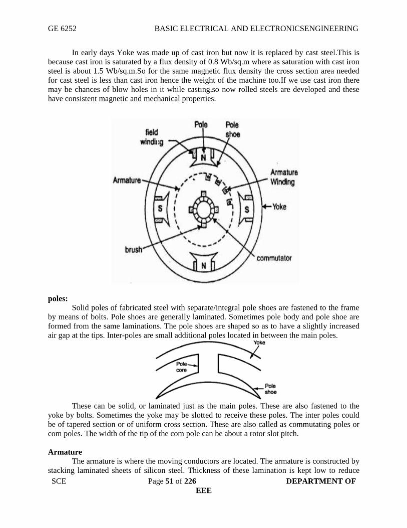
GE 6252 BASIC ELECTRICAL AND ELECTRONICSENGINEERING
SCE Page 51 of 226 DEPARTMENT OF
EEE
In early days Yoke was made up of cast iron but now it is replaced by cast steel.This is
because cast iron is saturated by a flux density of 0.8 Wb/sq.m where as saturation with cast iron
steel is about 1.5 Wb/sq.m.So for the same magnetic flux density the cross section area needed
for cast steel is less than cast iron hence the weight of the machine too.If we use cast iron there
may be chances of blow holes in it while casting.so now rolled steels are developed and these
have consistent magnetic and mechanical properties.
poles:
Solid poles of fabricated steel with separate/integral pole shoes are fastened to the frame
by means of bolts. Pole shoes are generally laminated. Sometimes pole body and pole shoe are
formed from the same laminations. The pole shoes are shaped so as to have a slightly increased
air gap at the tips. Inter-poles are small additional poles located in between the main poles.
These can be solid, or laminated just as the main poles. These are also fastened to the
yoke by bolts. Sometimes the yoke may be slotted to receive these poles. The inter poles could
be of tapered section or of uniform cross section. These are also called as commutating poles or
com poles. The width of the tip of the com pole can be about a rotor slot pitch.
Armature
The armature is where the moving conductors are located. The armature is constructed by
stacking laminated sheets of silicon steel. Thickness of these lamination is kept low to reduce

GE 6252 BASIC ELECTRICAL AND ELECTRONICSENGINEERING
SCE Page 52 of 226 DEPARTMENT OF
EEE
eddy current losses. As the laminations carry alternating flux the choice of suitable material,
insulation coating on the laminations, stacking it etc are to be done more carefully. The core is
divided into packets to facilitate ventilation. The winding cannot be placed on the surface of the
rotor due to the mechanical forces coming on the same. Open parallel sided equally spaced slots
are normally punched in the rotor laminations.
These slots house the armature winding. Large sized machines employ a spider on which
the laminations are stacked in segments. End plates are suitably shaped so as to serve as
’Winding supporters’. Armature construction process must ensure provision of sufficient axial
and radial ducts to facilitate easy removal of heat from the armature winding.
Field windings:
In the case of wound field machines (as against permanent magnet excited machines) the
field winding takes the form of a concentric coil wound around the main poles. These carry the
excitation current and produce the main field in the machine. Thus the poles are created
electromagnetically. Two types of windings are generally employed. In shunt winding large
number of turns of small section copper conductor isoused. The resistance of such winding
would be an order of magnitude larger than the armature winding resistance. In the case of series
winding a few turns of heavy cross section conductor is used. The resistance of such windings is
low and is comparable to armature resistance. Some machines may have both the windings on
the poles. The total ampere turns required to establish the necessary flux under the poles is
calculated from the magnetic circuit calculations. The total mmf required is divided equally
between north and south poles as the poles are produced in pairs. The mmf required to be shared
between shunt and series windings are apportioned as per the design requirements. As these
work on the same magnetic system they are in the form of concentric coils. Mmf ’per pole’ is
normally used in these calculations. Armature winding As mentioned earlier, if the armature
coils are wound on the surface of the armature, such construction becomes mechanically weak.
The conductors may fly away when the armature starts rotating. Hence the armature windings
are in general pre-formed, taped and lowered into the open slots on the armature. In the case of
small machines, they can be hand wound. The coils are prevented from flying out due to the
centrifugal forces by means of bands of steel wire on the surface of the rotor in small groves cut
into it. In the case of large machines slot wedges are additionally used to restrain the coils from
flying away. The end portion of the windings are taped at the free end and bound to the winding
carrier ring of the armature at the commutator end. The armature must be dynamically balanced
to reduce the centrifugal forces at the operating speeds. Compensating winding One may find a
bar winding housed in the slots on the pole shoes. This is mostly found in d.c. machines of very
large rating. Such winding is called compensating winding. In smaller machines, they may be
absent.

GE 6252 BASIC ELECTRICAL AND ELECTRONICSENGINEERING
SCE Page 53 of 226 DEPARTMENT OF
EEE
Commutator:
Commutator is the key element which made the d.c. machine of the present day possible.
It consists of copper segments tightly fastened together with mica/micanite insulating separators
on an insulated base. The whole commutator forms a rigid and solid assembly of insulated
copper strips and can rotate at high speeds. Each commutator segment is provided with a ’riser’
where the ends of the armature coils get connected. The surface of the commutator is machined
and surface is made concentric with the shaft and the current collecting brushes rest on the same.
Under-cutting the mica insulators that are between these commutator segments has to be done
periodically to avoid fouling of the surface of the commutator by mica when the commutator
gets worn out. Some details of the construction of the commutator are seen in Fig
Brush and brush holders:
Brushes rest on the surface of the commutator. Normally electro-graphite is used as brush
material. The actual composition of the brush depends on the peripheral speed of the commutator
and the working voltage. The hardness of the graphite brush is selected to be lower than that of
the commutator. When the brush wears out the graphite works as a solid lubricant reducing
frictional coefficient. More number of relatively smaller width brushes are preferred in place of
large broad brushes. The brush holders provide slots for the brushes to be placed. The connection
Brush holder with a Brush and Positioning of the brush on the commutator from the brush is
taken out by means of flexible pigtail. The brushes are kept pressed on the commutator with the
help of springs. This is to ensure proper contact between the brushes and the commutator even
under high speeds of operation. Jumping of brushes must be avoided to ensure arc free current
collection and to keep the brushcontact drop low. Other mechanical parts End covers, fan and
shaft bearings form other important mechanical parts. End covers are completely solid or have
opening for ventilation. They support the bearings which are on the shaft. Proper machining is to
be ensured for easy assembly. Fans can be external or internal. In most machines the fan is on the
non-commutator end sucking the air from the commutator end and throwing the same out.
Adequate quantity of hot air removal has to be ensured. Bearings Small machines employ ball
bearings at both ends. For larger machines roller bearings are used especially at the driving end.
The bearings are mounted press-fit on the shaft. They are housed inside the end shield in such a
manner that it is not necessary to remove the bearings from the shaft for dismantling.
End Shields or Bearings
If the armature diameter does not exceed 35 to 45 cm then in addition to poles end shields
or frame head with bearing are attached to the frame.If the armature diameter is greater than 1m
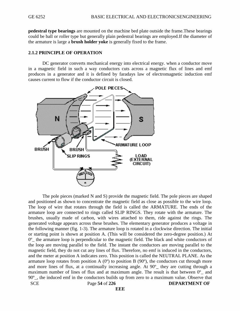
GE 6252 BASIC ELECTRICAL AND ELECTRONICSENGINEERING
SCE Page 54 of 226 DEPARTMENT OF
EEE
pedestral type bearings are mounted on the machine bed plate outside the frame.These bearings
could be ball or roller type but generally plain pedestral bearings are employed.If the diameter of
the armature is large a brush holder yoke is generally fixed to the frame.
2.1.2 PRINCIPLE OF OPERATION
DC generator converts mechanical energy into electrical energy. when a conductor move
in a magnetic field in such a way conductors cuts across a magnetic flux of lines and emf
produces in a generator and it is defined by faradays law of electromagnetic induction emf
causes current to flow if the conductor circuit is closed.
The pole pieces (marked N and S) provide the magnetic field. The pole pieces are shaped
and positioned as shown to concentrate the magnetic field as close as possible to the wire loop.
The loop of wire that rotates through the field is called the ARMATURE. The ends of the
armature loop are connected to rings called SLIP RINGS. They rotate with the armature. The
brushes, usually made of carbon, with wires attached to them, ride against the rings. The
generated voltage appears across these brushes. The elementary generator produces a voltage in
the following manner (fig. 1-3). The armature loop is rotated in a clockwise direction. The initial
or starting point is shown at position A. (This will be considered the zero-degree position.) At
0º_ the armature loop is perpendicular to the magnetic field. The black and white conductors of
the loop are moving parallel to the field. The instant the conductors are moving parallel to the
magnetic field, they do not cut any lines of flux. Therefore, no emf is induced in the conductors,
and the meter at position A indicates zero. This position is called the NEUTRAL PLANE. As the
armature loop rotates from position A (0º) to position B (90º), the conductors cut through more
and more lines of flux, at a continually increasing angle. At 90º_ they are cutting through a
maximum number of lines of flux and at maximum angle. The result is that between 0º_ and
90º_, the induced emf in the conductors builds up from zero to a maximum value. Observe that
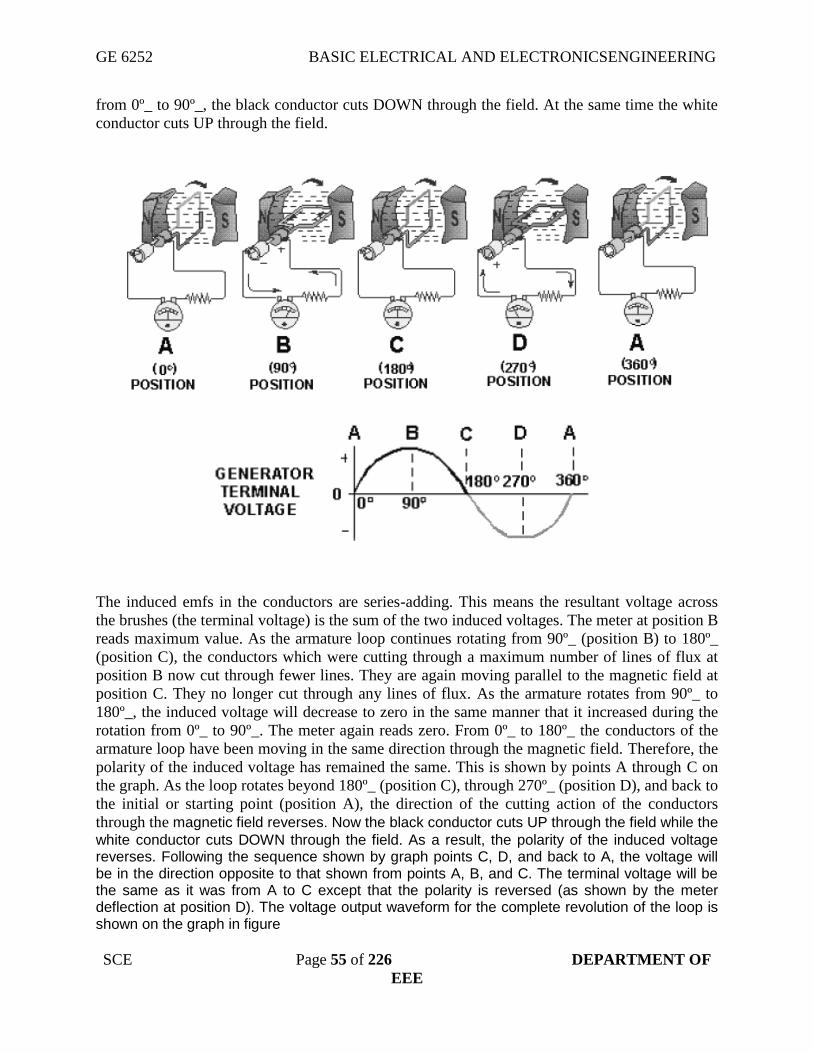
GE 6252 BASIC ELECTRICAL AND ELECTRONICSENGINEERING
SCE Page 55 of 226 DEPARTMENT OF
EEE
from 0º_ to 90º_, the black conductor cuts DOWN through the field. At the same time the white
conductor cuts UP through the field.
The induced emfs in the conductors are series-adding. This means the resultant voltage across
the brushes (the terminal voltage) is the sum of the two induced voltages. The meter at position B
reads maximum value. As the armature loop continues rotating from 90º_ (position B) to 180º_
(position C), the conductors which were cutting through a maximum number of lines of flux at
position B now cut through fewer lines. They are again moving parallel to the magnetic field at
position C. They no longer cut through any lines of flux. As the armature rotates from 90º_ to
180º_, the induced voltage will decrease to zero in the same manner that it increased during the
rotation from 0º_ to 90º_. The meter again reads zero. From 0º_ to 180º_ the conductors of the
armature loop have been moving in the same direction through the magnetic field. Therefore, the
polarity of the induced voltage has remained the same. This is shown by points A through C on
the graph. As the loop rotates beyond 180º_ (position C), through 270º_ (position D), and back to
the initial or starting point (position A), the direction of the cutting action of the conductors
through the magnetic field reverses. Now the black conductor cuts UP through the field while the
white conductor cuts DOWN through the field. As a result, the polarity of the induced voltage reverses. Following the sequence shown by graph points C, D, and back to A, the voltage will be in the direction opposite to that shown from points A, B, and C. The terminal voltage will be the same as it was from A to C except that the polarity is reversed (as shown by the meter deflection at position D). The voltage output waveform for the complete revolution of the loop is shown on the graph in figure
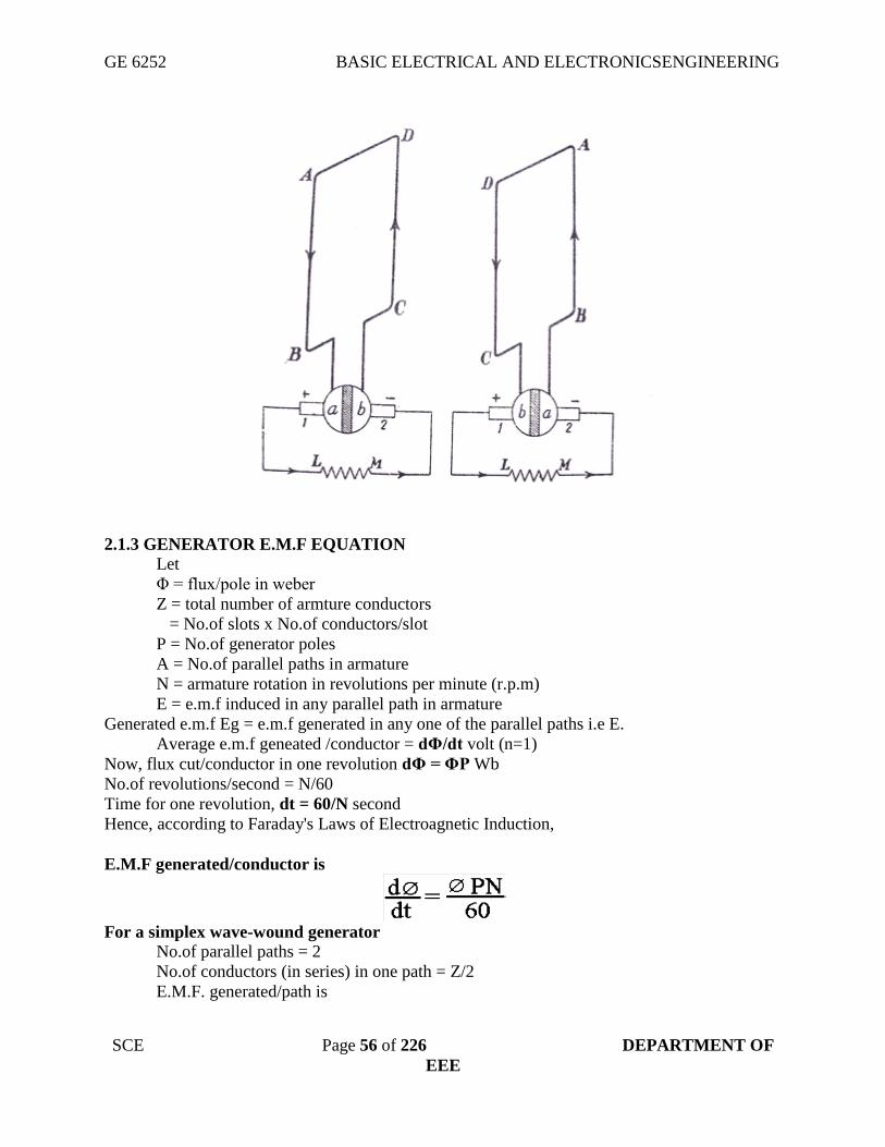
GE 6252 BASIC ELECTRICAL AND ELECTRONICSENGINEERING
SCE Page 56 of 226 DEPARTMENT OF
EEE
2.1.3 GENERATOR E.M.F EQUATION
Let
Φ = flux/pole in weber
Z = total number of armture conductors
= No.of slots x No.of conductors/slot
P = No.of generator poles
A = No.of parallel paths in armature
N = armature rotation in revolutions per minute (r.p.m)
E = e.m.f induced in any parallel path in armature
Generated e.m.f Eg = e.m.f generated in any one of the parallel paths i.e E.
Average e.m.f geneated /conductor = dΦ/dt volt (n=1)
Now, flux cut/conductor in one revolution dΦ = ΦP Wb
No.of revolutions/second = N/60
Time for one revolution, dt = 60/N second
Hence, according to Faraday's Laws of Electroagnetic Induction,
E.M.F generated/conductor is
For a simplex wave-wound generator
No.of parallel paths = 2
No.of conductors (in series) in one path = Z/2
E.M.F. generated/path is
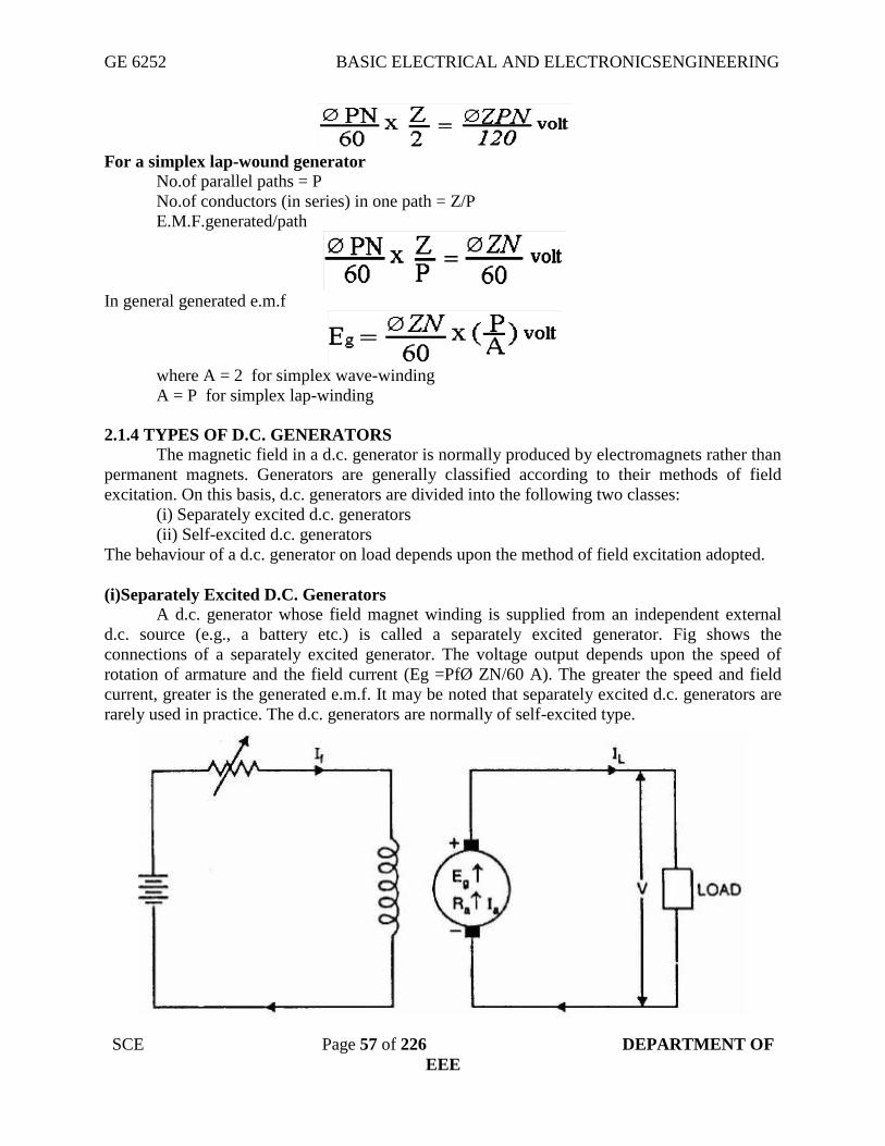
GE 6252 BASIC ELECTRICAL AND ELECTRONICSENGINEERING
SCE Page 57 of 226 DEPARTMENT OF
EEE
For a simplex lap-wound generator
No.of parallel paths = P
No.of conductors (in series) in one path = Z/P
E.M.F.generated/path
In general generated e.m.f
where A = 2 for simplex wave-winding
A = P for simplex lap-winding
2.1.4 TYPES OF D.C. GENERATORS
The magnetic field in a d.c. generator is normally produced by electromagnets rather than
permanent magnets. Generators are generally classified according to their methods of field
excitation. On this basis, d.c. generators are divided into the following two classes:
(i) Separately excited d.c. generators
(ii) Self-excited d.c. generators
The behaviour of a d.c. generator on load depends upon the method of field excitation adopted.
(i)Separately Excited D.C. Generators
A d.c. generator whose field magnet winding is supplied from an independent external
d.c. source (e.g., a battery etc.) is called a separately excited generator. Fig shows the
connections of a separately excited generator. The voltage output depends upon the speed of
rotation of armature and the field current (Eg =PfØ ZN/60 A). The greater the speed and field
current, greater is the generated e.m.f. It may be noted that separately excited d.c. generators are
rarely used in practice. The d.c. generators are normally of self-excited type.

GE 6252 BASIC ELECTRICAL AND ELECTRONICSENGINEERING
SCE Page 58 of 226 DEPARTMENT OF
EEE
Armature current, Ia = IL
Terminal voltage, V = Eg - IaRa
Electric power developed = EgIa
Power delivered to load = EgIa - Ia2Ra
(ii)Self-Excited D.C. Generators
A d.c. generator whose field magnet winding is supplied current from the output of the
generator itself is called a self-excited generator. There are three types of self-excited generators
depending upon the manner in which the field winding isconnected to the armature, namely;
(a) Series generator;
(b) Shunt generator;
(c) Compound generator
(a) Series generator
In a series wound generator, the field winding is connected in series with armature
winding so that whole armature current flows through the field winding as well as the load. Fig.
shows the connections of a series wound generator. Since the field winding carries the whole of
load current, it has a few turns of thick wire having low resistance. Series generators are rarely
used except for special purposes e.g., as boosters.
Armature current, Ia = Ise = IL = I(say)
Terminal voltage, V = EG - I(Ra + Rse)
Power developed in armature = EgIa
Power delivered to load
(b) Shunt generator
In a shunt generator, the field winding is connected in parallel with the armature winding
so that terminal voltage of the generator is applied across it. The shunt field winding has many
turns of fine wire having high resistance. Therefore, only a part of armature current flows

GE 6252 BASIC ELECTRICAL AND ELECTRONICSENGINEERING
SCE Page 59 of 226 DEPARTMENT OF
EEE
through shunt field winding and the rest flows through the load. Fig. shows the connections of a
shunt-wound generator.
Shunt field current, Ish = V/Rsh
Armature current, Ia = IL + Ish
Terminal voltage, V = Eg - IaRa
Power developed in armature = EgIa
Power delivered to load = VIL
(c) Compound generator
In a compound-wound generator, there are two sets of field windings on each pole—one
is in series and the other in parallel with the armature. A compound wound generator may be:
Short Shunt in which only shunt field winding is in parallel with the armature winding.Long
Shunt in which shunt field winding is in parallel with both series field and armature winding

GE 6252 BASIC ELECTRICAL AND ELECTRONICSENGINEERING
SCE Page 60 of 226 DEPARTMENT OF
EEE
2.1.5 GENERATOR CHARACTERISTICS:
The three most important characteristics or curves of a d.c generator are
1. OpenCircuitCharacteristic (O.C.C.)
This curve shows the relation between the generated e.m.f. at no-load (E0) and the field
current (If) at constant speed. It is also known as magnetic characteristic or no-load saturation
curve. Its shape is practically the same for all generators whether separately or self-excited. The
data for O.C.C. curve are obtained experimentally by operating the generator at no load and
constant speed and recording the change in terminal voltage as the field current is varied.
2. Internal or Total characteristic (E/Ia)
This curve shows the relation between the generated e.m.f. on load (E) and the armature
current (Ia). The e.m.f. E is less than E0 due to the demagnetizing effect of armature reaction.
Therefore, this curve will lie below the open circuit characteristic (O.C.C.). The internal
characteristic is of interest chiefly to the designer. It cannot be obtained directly by experiment.
It is because a voltmeter cannot read the e.m.f. generated on load due to the voltage drop in
armature resistance. The internal characteristic can be obtained from external characteristic if
winding resistances are known because armature reaction effect is included in both
characteristics
3. External characteristic (V/IL)

GE 6252 BASIC ELECTRICAL AND ELECTRONICSENGINEERING
SCE Page 61 of 226 DEPARTMENT OF
EEE
This curve shows the relation between the terminal voltage (V) and load current (IL). The
terminal voltage V will be less than E due to voltage drop in the armature circuit. Therefore, this
curve will lie below the internal characteristic. This characteristic is very important in
determining the suitability of a generator for a given purpose. It can be obtained by making
simultaneous
2.1.5.1 characteristics Series of DC generator: Fig. shows the connections of a series wound generator. Since there is only one current (that
which flows through the whole machine), the load currentis the same as the exciting current.
(i)O.C.C.
Curve 1 shows the open circuit characteristic (O.C.C.) of a series generator. It can be
obtainedexperimentally by disconnecting the field winding from the machine and exciting it
from aseparate d.c. source
(ii) Internal characteristic
Curve 2 shows the total or internal characteristic of a series generator. It gives the relation
between the generated e.m.f. E. on load and armature current. Due to armature reaction, the flux
in the machine will be less than the flux at no load. Hence, e.m.f. E generated under load
conditions will be less than the e.m.f. EO generated under no load conditions. Consequently,
internal characteristic curve generated under no load conditions. Consequently, internal
characteristic curve lies below the O.C.C. curve; the difference between them representing the
effect of armature reaction
(iii)Externalcharacteristic
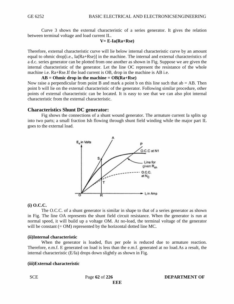
GE 6252 BASIC ELECTRICAL AND ELECTRONICSENGINEERING
SCE Page 62 of 226 DEPARTMENT OF
EEE
Curve 3 shows the external characteristic of a series generator. It gives the relation
between terminal voltage and load current IL.
V= E-Ia(Ra+Rse)
Therefore, external characteristic curve will lie below internal characteristic curve by an amount
equal to ohmic drop[i.e., Ia(Ra+Rse)] in the machine. The internal and external characteristics of
a d.c. series generator can be plotted from one another as shown in Fig. Suppose we are given the
internal characteristic of the generator. Let the line OC represent the resistance of the whole
machine i.e. Ra+Rse.If the load current is OB, drop in the machine is AB i.e.
AB = Ohmic drop in the machine = OB(Ra+Rse)
Now raise a perpendicular from point B and mark a point b on this line such that ab = AB. Then
point b will lie on the external characteristic of the generator. Following similar procedure, other
points of external characteristic can be located. It is easy to see that we can also plot internal
characteristic from the external characteristic.
Characteristics Shunt DC generator: Fig shows the connections of a shunt wound generator. The armature current Ia splits up
into two parts; a small fraction Ish flowing through shunt field winding while the major part IL
goes to the external load.
(i) O.C.C.
The O.C.C. of a shunt generator is similar in shape to that of a series generator as shown
in Fig. The line OA represents the shunt field circuit resistance. When the generator is run at
normal speed, it will build up a voltage OM. At no-load, the terminal voltage of the generator
will be constant (= OM) represented by the horizontal dotted line MC.
(ii)Internal characteristic
When the generator is loaded, flux per pole is reduced due to armature reaction.
Therefore, e.m.f. E generated on load is less than the e.m.f. generated at no load.As a result, the
internal characteristic (E/Ia) drops down slightly as shown in Fig.
(iii)External characteristic
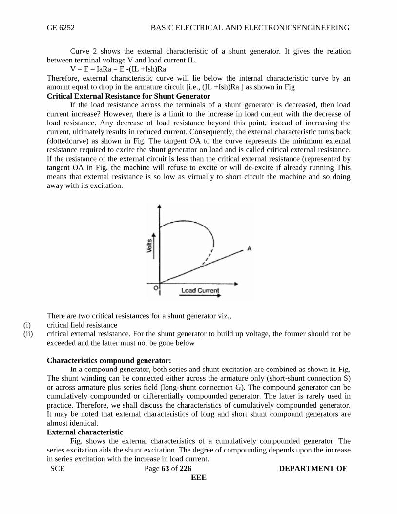
GE 6252 BASIC ELECTRICAL AND ELECTRONICSENGINEERING
SCE Page 63 of 226 DEPARTMENT OF
EEE
Curve 2 shows the external characteristic of a shunt generator. It gives the relation
between terminal voltage V and load current IL.
V = E – IaRa = E -(IL +Ish)Ra
Therefore, external characteristic curve will lie below the internal characteristic curve by an
amount equal to drop in the armature circuit [i.e., (IL +Ish)Ra ] as shown in Fig
Critical External Resistance for Shunt Generator
If the load resistance across the terminals of a shunt generator is decreased, then load
current increase? However, there is a limit to the increase in load current with the decrease of
load resistance. Any decrease of load resistance beyond this point, instead of increasing the
current, ultimately results in reduced current. Consequently, the external characteristic turns back
(dottedcurve) as shown in Fig. The tangent OA to the curve represents the minimum external
resistance required to excite the shunt generator on load and is called critical external resistance.
If the resistance of the external circuit is less than the critical external resistance (represented by
tangent OA in Fig, the machine will refuse to excite or will de-excite if already running This
means that external resistance is so low as virtually to short circuit the machine and so doing
away with its excitation.
There are two critical resistances for a shunt generator viz.,
(i) critical field resistance
(ii) critical external resistance. For the shunt generator to build up voltage, the former should not be
exceeded and the latter must not be gone below
Characteristics compound generator:
In a compound generator, both series and shunt excitation are combined as shown in Fig.
The shunt winding can be connected either across the armature only (short-shunt connection S)
or across armature plus series field (long-shunt connection G). The compound generator can be
cumulatively compounded or differentially compounded generator. The latter is rarely used in
practice. Therefore, we shall discuss the characteristics of cumulatively compounded generator.
It may be noted that external characteristics of long and short shunt compound generators are
almost identical.
External characteristic
Fig. shows the external characteristics of a cumulatively compounded generator. The
series excitation aids the shunt excitation. The degree of compounding depends upon the increase
in series excitation with the increase in load current.

GE 6252 BASIC ELECTRICAL AND ELECTRONICSENGINEERING
SCE Page 64 of 226 DEPARTMENT OF
EEE
(i) If series winding turns are so adjusted that with the increase in load current the terminal
voltage increases, it is called over-compounded generator. In such a case, as the load current
increases, the series field m.m.f. increases and tends to increase the flux and hence the generated
voltage. The increase in generated voltage is greater than the IaRa drop so that instead of
decreasing, the terminal voltage increases as shown by curve A in Fig.
(ii) If series winding turns are so adjusted that with the increase in load current, the terminal
voltage substantially remains constant, it is called flat-compounded generator. The series
winding of such a machine has lesser number of turns than the one in over-compounded machine
and, therefore, does not increase the flux as much for a given load current. Consequently, the
full-load voltage is nearly equal to the no-load voltage as indicated by curve B in Fig
(iii) If series field winding has lesser number of turns than for a flat compounded machine, the
terminal voltage falls with increase in load current as indicated by curve C m Fig. Such a
machine is called under-compounded generator.
2.1.6 APPLICATIONS OF DC GENERATOR
DC Separately Exited Generator: As a supply source to DC Motors, whose speed is to be controlled for certain
applications. Where a wide range of voltage is required for the testing purposes.
DC Shunt Generator
The terminal voltage of DC shunt generator is more or less constant from no load to full
load .Therefore these generators are used where constant voltage is required.
For electro plating
Battery charging
For excitation of Alternators.

GE 6252 BASIC ELECTRICAL AND ELECTRONICSENGINEERING
SCE Page 65 of 226 DEPARTMENT OF
EEE
DC Series Generator
The terminal voltage of series generator increases with load current from no load to full
load .Therefore these generators are,
Used as Boosters
Used for supply to arc Lamps
DC Compound Generator: Differential Compound generators are used to supply dc welding machines. Level compound
generators are used to supply power for offices, hostels and Lodges etc. Over compound
generators are used to compensate the voltage drop in Feeders.
2.2 DC MOTOR - INTRODUCTION
A machine that converts dc power into mechanical energy is known as dc motor. Its
operation is based on the principle that when a current carrying conductor is placed in a magnetic
field, the conductor experiences a mechanical force. The direction of the force is given by
Fleming’s left hand rule.
How DC motors work?
There are different kinds of D.C. motors, but they all work on the same principles.When
a permanent magnet is positioned around a loop of wire that is hooked up to a D.C. power
source, we have the basics of a D.C. motor. In order to make the loop of wire spin, we have to
connect a battery or DC power supply between its ends, and support it so it can spin about its
axis. To allow the rotor to turn without twisting the wires, the ends of the wire loop are
connected to a set of contacts called the commutator, which rubs against a set of conductors
called the brushes. The brushes make electrical contact with the commutator as it spins, and are
connected to the positive and negative leads of the power source, allowing electricity to flow
through the loop. The electricity flowing through the loop creates a magnetic field that interacts
with the magnetic field of the permanent magnet to make the loop spin.
2.2.1 PRINCIPLES OF OPERATION It is based on the principle that when a current-carrying conductor is placed in a magnetic
field, it experiences a mechanical force whose direction is given by Fleming's Left-hand rule and
whose magnitude is given by
Force, F = B I l newton
Where B is the magnetic field in weber/m2.
I is the current in amperes and
l is the length of the coil in meter.
The force, current and the magnetic field are all in different directions.
If an Electric current flows through two copper wires that are between the poles of a magnet, an
upward force will move one wire up and a downward force will move the other wire down.

GE 6252 BASIC ELECTRICAL AND ELECTRONICSENGINEERING
SCE Page 66 of 226 DEPARTMENT OF
EEE
2.2.2 BACK OR COUNTER EMF
When the armature of a d.c. motor rotates under the influence of the driving torque, the
armature conductors move through the magnetic field and hence an e.m.f. is induced in them.
The induced e.m.f. acts in opposite direction to the applied voltage V(Lenz’s law) and is known
as back orcounter e.m.f. Eb.

GE 6252 BASIC ELECTRICAL AND ELECTRONICSENGINEERING
SCE Page 67 of 226 DEPARTMENT OF
EEE
2.2.3 SIGNIFICANCE OF BACK E.M.F
The presence of back e.m.f. makes the d.c. motor a self-regulating machine i.e., it makes
the motor to draw as much armature current as is just sufficient to develop the torque required by
the load. Back e.m.f. in a d.c. motor regulates the flow of armature current i.e., it automatically
changes the armature current to meet the load requirement.
2.2.4 CLASSIFICATION OF MOTOR
DC motors are more common than we may think. A car may have as many as 20 DC
motors to drive fans, seats, and windows. They come in three different types, classified
according to the electrical circuit used. In the shunt motor, the armature and field windings are
connected in parallel, and so the currents through each are relatively independent. The current
through the field winding can be controlled with a field rheostat (variable resistor), thus allowing
a wide variation in the motor speed over a large range of load conditions. This type of motor is
used for driving machine tools or fans, which require a wide range of speeds.
In the series motor, the field winding is connected in series with the armature winding,
resulting in a very high starting torque since both the armature current and field strength run at
their maximum. However, once the armature starts to rotate, the counter EMF reduces the
current in the circuit, thus reducing the field strength. The series motor is used where a large
starting torque is required, such as in automobile starter motors, cranes, and hoists.
The compound motor is a combination of the series and shunt motors, having parallel and series
field windings. This type of motor has a high starting torque and the ability to vary the speed and
is used in situations requiring both these properties such as punch presses, conveyors and
elevators.

GE 6252 BASIC ELECTRICAL AND ELECTRONICSENGINEERING
SCE Page 68 of 226 DEPARTMENT OF
EEE
2.2.5 DC MOTOR TYPES
1. Shunt Wound
2. Series Wound
3. Compound wound
1. Shunt Motor
In shunt wound motor the field winding is connected in parallel with armature. The
current through the shunt field winding is not the same as the armature current. Shunt field
windings are designed to produce the necessary m.m.f. by means of a relatively large number of
turns of wire having high resistance. Therefore, shunt field current is relatively small compared
with the armature current
2. Series Motor
In series wound motor the field winding is connected in series with the armature.
Therefore, series field winding carries the armature current. Since the current passing through a
series field winding is the same as the armature current, series field windings must be designed
with much fewer turns than shunt field windings for the same mmf.Therefore, a series field
winding has a relatively small number of turns of thick wire and, therefore, will possess a low
resistance.
3. Compound Wound Motor
Compound wound motor has two field windings; one connected in parallel with the
armature and the other in series with it. There are two types of compound motor connections
1) Short-shunt connection

GE 6252 BASIC ELECTRICAL AND ELECTRONICSENGINEERING
SCE Page 69 of 226 DEPARTMENT OF
EEE
2) Long shunt connection
When the shunt field winding is directly connected across the armature terminals it is called
short-shunt connection.
When the shunt winding is so connected that it shunts the series combination of armature and
series field it is called long-shunt connection.
2.2.6 VOLTAGE EQUATION OF MOTORS
Let in a d.c. motor V = applied voltage Eb = back e.m.f. Ra = armature resistance Ia = armature current
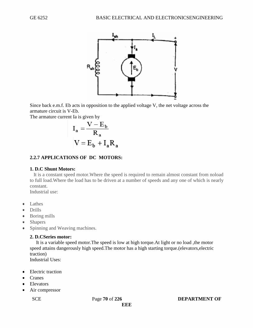
GE 6252 BASIC ELECTRICAL AND ELECTRONICSENGINEERING
SCE Page 70 of 226 DEPARTMENT OF
EEE
Since back e.m.f. Eb acts in opposition to the applied voltage V, the net voltage across the
armature circuit is V-Eb.
The armature current Ia is given by
2.2.7 APPLICATIONS OF DC MOTORS:
1. D.C Shunt Motors: It is a constant speed motor.Where the speed is required to remain almost constant from noload
to full load.Where the load has to be driven at a number of speeds and any one of which is nearly
constant.
Industrial use:
Lathes
Drills
Boring mills
Shapers
Spinning and Weaving machines.
2. D.CSeries motor: It is a variable speed motor.The speed is low at high torque.At light or no load ,the motor
speed attains dangerously high speed.The motor has a high starting torque.(elevators,electric
traction)
Industrial Uses:
Electric traction
Cranes
Elevators
Air compressor
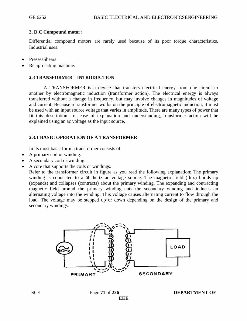
GE 6252 BASIC ELECTRICAL AND ELECTRONICSENGINEERING
SCE Page 71 of 226 DEPARTMENT OF
EEE
3. D.C Compound motor:
Differential compound motors are rarely used because of its poor torque characteristics.
Industrial uses:
PressesShears
Reciprocating machine.
2.3 TRANSFORMER – INTRODUCTION
A TRANSFORMER is a device that transfers electrical energy from one circuit to
another by electromagnetic induction (transformer action). The electrical energy is always
transferred without a change in frequency, but may involve changes in magnitudes of voltage
and current. Because a transformer works on the principle of electromagnetic induction, it must
be used with an input source voltage that varies in amplitude. There are many types of power that
fit this description; for ease of explanation and understanding, transformer action will be
explained using an ac voltage as the input source.
2.3.1 BASIC OPERATION OF A TRANSFORMER
In its most basic form a transformer consists of:
A primary coil or winding.
A secondary coil or winding.
A core that supports the coils or windings.
Refer to the transformer circuit in figure as you read the following explanation: The primary
winding is connected to a 60 hertz ac voltage source. The magnetic field (flux) builds up
(expands) and collapses (contracts) about the primary winding. The expanding and contracting
magnetic field around the primary winding cuts the secondary winding and induces an
alternating voltage into the winding. This voltage causes alternating current to flow through the
load. The voltage may be stepped up or down depending on the design of the primary and
secondary windings.

GE 6252 BASIC ELECTRICAL AND ELECTRONICSENGINEERING
SCE Page 72 of 226 DEPARTMENT OF
EEE
2.3.2 AN IDEAL TRANSFORMER
An ideal transformer is shown in the adjacent figure. Current passing through the primary
coil creates a magnetic field. The primary and secondary coils are wrapped around a core of very
high magnetic permeability, such as iron, so that most of the magnetic flux passes through both
the primary and secondary coils.
2.3.3 BASIC WORKING PRINCIPLE OF TRANSFORMER
A transformer can be defined as a static device which helps in the transformation of
electric power in one circuit to electric power of the same frequency in another circuit. The
voltage can be raised or lowered in a circuit, but with a proportional increase or decrease in the
current ratings.
The main principle of operation of a transformer is mutual inductance between two
circuits which is linked by a common magnetic flux. A basic transformer consists of two coils
that are electrically separate and inductive, but are magnetically linked through a path of
reluctance. The working principle of the transformer can be understood from the figure below.
As shown above the transformer has primary and secondary windings. The core
laminations are joined in the form of strips in between the strips you can see that there are some
narrow gaps right through the cross-section of the core. These staggered joints are said to be
‘imbricated’. Both the coils have high mutual inductance. A mutual electro-motive force is
induced in the transformer from the alternating flux that is set up in the laminated core, due to
the coil that is connected to a source of alternating voltage. Most of the alternating flux
developed by this coil is linked with the other coil and thus produces the mutual induced electro-
motive force. The so produced electro-motive force can be explained with the help of Faraday’s
laws of Electromagnetic Induction as
e=M*dI/dt
If the second coil circuit is closed, a current flows in it and thus electrical energy is transferred
magnetically from the first to the second coil.

GE 6252 BASIC ELECTRICAL AND ELECTRONICSENGINEERING
SCE Page 73 of 226 DEPARTMENT OF
EEE
The alternating current supply is given to the first coil and hence it can be called as the primary
winding. The energy is drawn out from the second coil and thus can be called as the secondary
winding.
In short, a transformer carries the operations shown below:
Transfer of electric power from one circuit to another.
Transfer of electric power without any change in frequency.
Transfer with the principle of electromagnetic induction.
The two electrical circuits are linked by mutual induction
2.3.4 TRANSFORMER CONSTRUCTION
Two coils of wire (called windings) are wound on some type of core material. In some
cases the coils of wire are wound on a cylindrical or rectangular cardboard form. In effect, the
core material is air and the transformer is called an AIR-CORE TRANSFORMER. Transformers
used at low frequencies, such as 60 hertz and 400 hertz, require a core of low-reluctance
magnetic material, usually iron. This type of transformer is called an IRON-CORE
TRANSFORMER. Most power transformers are of the iron-core type.
The principle parts of a transformer and their functions are:
• The CORE, which provides a path for the magnetic lines of flux.
• The PRIMARY WINDING, which receives energy from the ac source.
• The SECONDARY WINDING, which receives energy from the primary winding and delivers it
to the load.
• The ENCLOSURE, which protects the above components from dirt, moisture, and mechanical
damage.
(i) CORE

GE 6252 BASIC ELECTRICAL AND ELECTRONICSENGINEERING
SCE Page 74 of 226 DEPARTMENT OF
EEE
There are two main shapes of cores used in laminated-steel-core transformers. One is the
HOLLOWCORE, so named because the core is shaped with a hollow square through the center.
This shape of core. Notice that the core is made up of many laminations of steel it shows how the
transformer windings are wrapped around both sides of the core.
(ii) WINDINGS
As stated above, the transformer consists of two coils called WINDINGS which are
wrapped around a core. The transformer operates when a source of ac voltage is connected to
one of the windings and a load device is connected to the other. The winding that is connected to
the source is called the PRIMARY WINDING. The winding that is connected to the load is
called the SECONDARY WINDING. The primary is wound in layers directly on a rectangular
cardboard form.
2.3.5 EMF Equation of Transformer:
Let the applied voltage V1 applied to the primary of a transformer, with secondary open-
circuited, be sinusoidal (or sine wave). Then the current I1, due to applied voltage V1, will also
be a sine wave. The mmf N1 I1 and core flux Ø will follow the variations of I1 closely. That is
the flux is in time phase with the current I1 and varies sinusoidally.
Let,
NA = Number of turns in primary
NB = Number of turns in secondary
Ømax = Maximum flux in the core in webers = Bmax X A
f = Frequency of alternating current input in hertz (HZ)
As shown in figure above, the core flux increases from its zero value to maximum value Ømax in
one quarter of the cycle , that is in ¼ frequency second.
Therefore, average rate of change of flux = Ømax/ ¼ f = 4f ØmaxWb/s
Now, rate of change of flux per turn means induced electro motive force in volts.
Therefore,
average electro-motive force induced/turn = 4f Ømaxvolt
If flux Ø varies sinusoidally, then r.m.s value of induced e.m.f is obtained by multiplying the
average value with form factor.
Form Factor = r.m.s. value/average value = 1.11
Therefore, r.m.s value of e.m.f/turn = 1.11 X 4f Ømax = 4.44f Ømax
Now, r.m.s value of induced e.m.f in the whole of primary winding
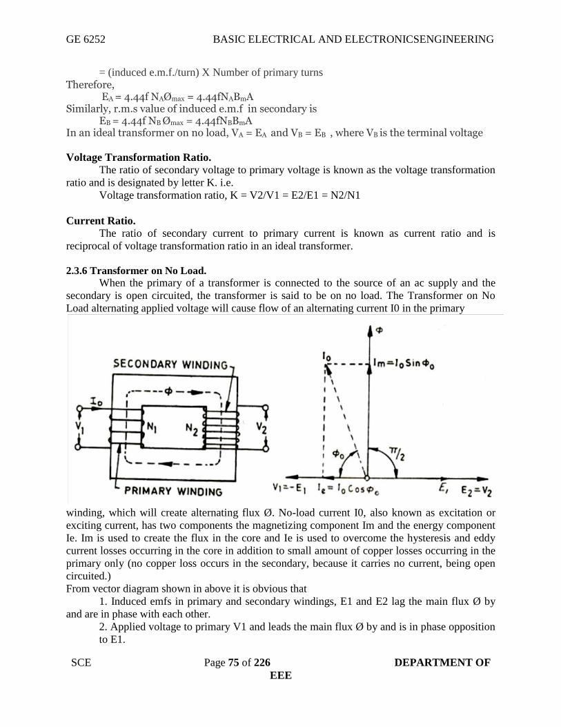
GE 6252 BASIC ELECTRICAL AND ELECTRONICSENGINEERING
SCE Page 75 of 226 DEPARTMENT OF
EEE
= (induced e.m.f./turn) X Number of primary turns Therefore,
EA = 4.44f NAØmax = 4.44fNABmA Similarly, r.m.s value of induced e.m.f in secondary is
EB = 4.44f NB Ømax = 4.44fNBBmA In an ideal transformer on no load, VA = EA and VB = EB , where VB is the terminal voltage
Voltage Transformation Ratio.
The ratio of secondary voltage to primary voltage is known as the voltage transformation
ratio and is designated by letter K. i.e.
Voltage transformation ratio, K = V2/V1 = E2/E1 = N2/N1
Current Ratio.
The ratio of secondary current to primary current is known as current ratio and is
reciprocal of voltage transformation ratio in an ideal transformer.
2.3.6 Transformer on No Load.
When the primary of a transformer is connected to the source of an ac supply and the
secondary is open circuited, the transformer is said to be on no load. The Transformer on No
Load alternating applied voltage will cause flow of an alternating current I0 in the primary
winding, which will create alternating flux Ø. No-load current I0, also known as excitation or
exciting current, has two components the magnetizing component Im and the energy component
Ie. Im is used to create the flux in the core and Ie is used to overcome the hysteresis and eddy
current losses occurring in the core in addition to small amount of copper losses occurring in the
primary only (no copper loss occurs in the secondary, because it carries no current, being open
circuited.)
From vector diagram shown in above it is obvious that
1. Induced emfs in primary and secondary windings, E1 and E2 lag the main flux Ø by
and are in phase with each other.
2. Applied voltage to primary V1 and leads the main flux Ø by and is in phase opposition
to E1.

GE 6252 BASIC ELECTRICAL AND ELECTRONICSENGINEERING
SCE Page 76 of 226 DEPARTMENT OF
EEE
3. Secondary voltage V2 is in phase and equal to E2 since there is no voltage drop in
secondary.
4. Im is in phase with Ø and so lags V1 by
5. Ie is in phase with the applied voltage V1.
6. Input power on no load = V1Ie = V1I0 cos Ø0 where Ø0 = tan-1
2.3.7 Transformer on Load:
The transformer is said to be loaded, when its secondary circuit is completed through an
impedance or load. The magnitude and phase of secondary current (i.e. current flowing through
secondary) I2 with respect to secondary terminals depends upon the characteristic of the load i.e.
current I2 will be in phase, lag behind and lead the terminal voltage V+2+ respectively when the
load is non-inductive, inductive and capacitive. The net flux passing through the core remains
almost constant from no-load to full load irrespective of load conditions and so core losses
remain almost constant from no-load to full load. Vector diagram for an ideal transformer
supplying inductive load is shown
Resistance and Leakage Reactance In actual practice, both of the primary and secondary
windings have got some ohmic resistance causing voltage drops and copper losses in the
windings. In actual practice, the total flux created does not link both of the primary and
secondary windings but is divided into three components namely the main or mutual flux Ø

GE 6252 BASIC ELECTRICAL AND ELECTRONICSENGINEERING
SCE Page 77 of 226 DEPARTMENT OF
EEE
linking both of the primary and secondary windings, primary leakage flux ØL1 linking with
primary winding only and secondary leakage flux ØL2 linking with secondary winding only. The
primary leakage flux ØL1 is produced by primary ampere-turns and is proportional to primary
current, number of primary turns being fixed. The primary leakage flux ØL1 is in phase with I1
and produces self induced emf ØL1 is in phase with I1 and produces self induced emf EL1 given
as 2f L1 I1 in the primary winding.
The self induced emf divided by the primary current gives the reactance of primary and is
denoted by X1.
i.e. X1 = EL1/I1 = 2πfL1I1/I1 = 2FL1,
Similarly leakage reactance of secondary X2 = EL2/E2 = 2fπL2I2/I2 = 2πfL2
Equivalent Resistance and Reactance. The equivalent resistances and reactance’s of transformer
windings referred to primary and secondary sides are given as below Referred to primary side
Equivalent resistance,
Equivalent resistance, = X'1 = Referred to secondary side
Equivalent resistance,
Equivalent resistance, = X2 + K2X1
Where K is the transformation ratio.
2.3.8 EQUIVALENT CIRCUIT OF TRANSFORMER
Equivalent impedance of transformer is essential to be calculated because the electrical
power transformer is an electrical power system equipment for estimating different parameters of
electrical power system which may be required to calculate total internal impedance of
an electrical power transformer, viewing from primary side or secondary side as per requirement.
This calculation requires equivalent circuit of transformer referred to primary or equivalent
circuit of transformer referred to secondary sides respectively. Percentage impedance is also
very essential parameter of transformer. Special attention is to be given to this parameter during
installing a transformer in an existing electrical power system. Percentage impedance of different
power transformers should be properly matched during parallel operation of power transformers.
The percentage impedance can be derived from equivalent impedance of transformer so, it can
be said that equivalent circuit of transformer is also required during calculation of %
impedance.
Equivalent Circuit of Transformer Referred to Primary
For drawing equivalent circuit of transformer referred to primary, first we have to
establish general equivalent circuit of transformer then, we will modify it for referring from
primary side. For doing this, first we need to recall the complete vector diagram of a transformer
which is shown in the figure below.

GE 6252 BASIC ELECTRICAL AND ELECTRONICSENGINEERING
SCE Page 78 of 226 DEPARTMENT OF
EEE
Let us consider the transformation ratio be,
In the figure right, the applied voltage to the primary is V1 and voltage across the primary
winding is E1. Total current supplied to primary is I1. So the voltage V1 applied to the primary is
partly dropped by I1Z1 or I1R1 + j.I1X1 before it appears across primary winding. The
voltage appeared across winding is countered by primary induced emf E1.
The equivalent circuit for that equation can be drawn as below,
From the vector diagram above, it is found that the total primary current I1 has two components,
one is no - load component Io and the other is load component I2′. As this primary current has
two a component or branches, so there must be a parallel path with primary winding of
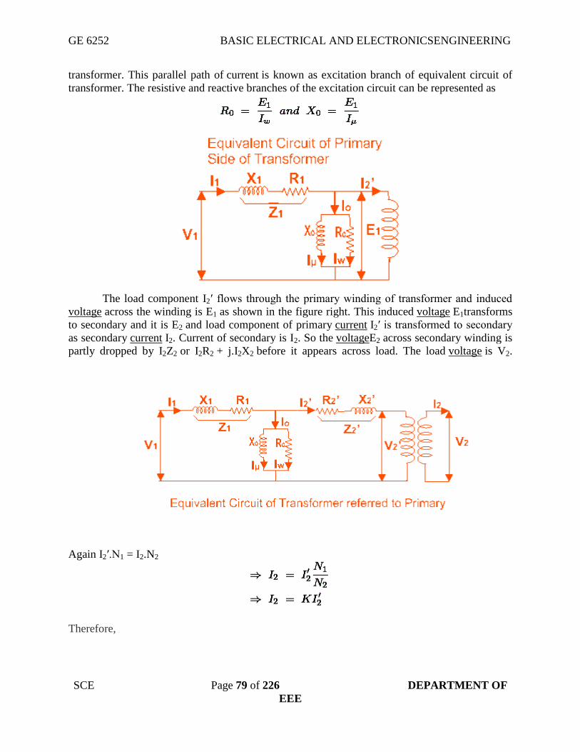
GE 6252 BASIC ELECTRICAL AND ELECTRONICSENGINEERING
SCE Page 79 of 226 DEPARTMENT OF
EEE
transformer. This parallel path of current is known as excitation branch of equivalent circuit of
transformer. The resistive and reactive branches of the excitation circuit can be represented as
The load component I2′ flows through the primary winding of transformer and induced
voltage across the winding is E1 as shown in the figure right. This induced voltage E1transforms
to secondary and it is E2 and load component of primary current I2′ is transformed to secondary
as secondary current I2. Current of secondary is I2. So the voltageE2 across secondary winding is
partly dropped by I2Z2 or I2R2 + j.I2X2 before it appears across load. The load voltage is V2.
Again I2′.N1 = I2.N2
Therefore,

GE 6252 BASIC ELECTRICAL AND ELECTRONICSENGINEERING
SCE Page 80 of 226 DEPARTMENT OF
EEE
From above equation, secondary impedance of transformer referred to primary is,
So, the complete equivalent circuit of transformer referred to primary is shown in the figure
below,
Approximate Equivalent Circuit of Transformer
Since Io is very small compared to I1, it is less than 5% of full load primary current, Iochanges
the voltage drop insignificantly. Hence, it is good approximation to ignore the excitation circuit
in approximate equivalent circuit of transformer. The winding resistanceand reactance being in
series can now be combined into equivalent resistance and reactance of transformer, referred to
any particular side. In this case it is side 1 or primary side.

GE 6252 BASIC ELECTRICAL AND ELECTRONICSENGINEERING
SCE Page 81 of 226 DEPARTMENT OF
EEE
Equivalent Circuit of Transformer Referred to Secondary
In similar way, approximate equivalent circuit of transformer referred to secondary can
be drawn. Where equivalent impedance of transformer referred to secondary, can be derived as
2.3.9 VOLTAGE REGULATION
The voltage regulation is the percentage of voltage difference between no load and full
load voltages of a transformer with respect to its full load voltage.
GE 6252 BASIC ELECTRICAL AND ELECTRONICSENGINEERING
SCE Page 82 of 226 DEPARTMENT OF
EEE
Explanation of Voltage Regulation of Transformer
Say an electrical power transformer is open circuited, means load is not connected with
secondary terminals. In this situation, the secondary terminalvoltage of the transformer will be its
secondary induced emf E2. Whenever full load is connected to the secondary terminals of the
transformer, ratedcurrent I2 flows through the secondary circuit and voltage drop comes into
picture. At this situation, primary winding will also draw equivalent full load current from
source. The voltagedrop in the secondary is I2Z2 where Z2 is the secondary impedance of
transformer. Now if at this loading condition, any one measures the voltage between secondary
terminals, he or she will getvoltage V2 across load terminals which is obviously less than no load
secondary voltage E2and this is because of I2Z2 voltage drop in the transformer.
Expression of Voltage Regulation of Transformer, represented in percentage, is
2.4 SINGLE PHASE INDUCTION MOTOR – INTRODUCTION
The single-phase induction machine is the most frequently used motor for refrigerators, washing
machines, clocks, drills, compressors, pumps, and so forth.
• The single-phase motor stator has a laminated iron core with two windings arranged
perpendicularly.
• One is the main and
• The other is the auxiliary winding or starting winding
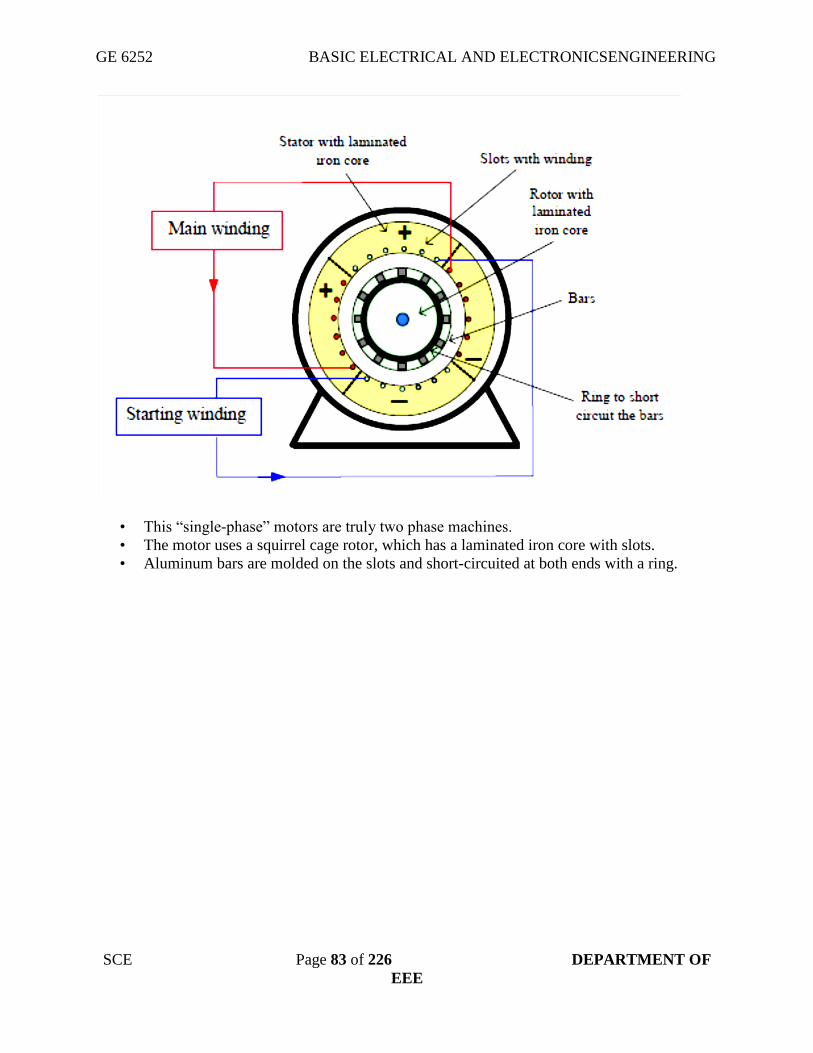
GE 6252 BASIC ELECTRICAL AND ELECTRONICSENGINEERING
SCE Page 83 of 226 DEPARTMENT OF
EEE
• This “single-phase” motors are truly two phase machines.
• The motor uses a squirrel cage rotor, which has a laminated iron core with slots.
• Aluminum bars are molded on the slots and short-circuited at both ends with a ring.

GE 6252 BASIC ELECTRICAL AND ELECTRONICSENGINEERING
SCE Page 84 of 226 DEPARTMENT OF
EEE
The single-phase induction motor operation can be described by two methods:
• Double revolving field theory; and
• Cross-field theory.
Double revolving theory is perhaps the easier of the two explanations to understand
Double revolving field theory
• A single-phase ac current supplies the main winding that produces a pulsating magnetic
field.
• Mathematically, the pulsating field could be divided into two fields, which are rotating in
opposite directions.
• The interaction between the fields and the current induced in the rotor bars generates
opposing torque
2.4.1 STARTING METHODS
The single-phase IM has no starting torque, but has resultant torque, when it
rotates at any other speed, except synchronous speed. It is also known that, in a balanced
two-phase IM having two windings, each having equal number of turns and placed at a
space angle of 900(electrical), and are fed from a balanced two-phase supply, with two
voltages equal in magnitude, at an angle of 900, the rotating magnetic fields are produced,
as in a three-phase IM. The torque-speed characteristic is same as that of a three-phase
one, having both starting and also running torque as shown earlier. So, in a single-phase
IM, if an auxiliary winding is introduced in the stator, in addition to the main winding,
but placed at a space angle of 900 (electrical), starting torque is produced. The currents in
the two (main and auxiliary) stator windings also must be at an angle of 900 , to produce

GE 6252 BASIC ELECTRICAL AND ELECTRONICSENGINEERING
SCE Page 85 of 226 DEPARTMENT OF
EEE
maximum starting torque, as shown in a balanced two-phase stator. Thus, rotating
magnetic field is produced in such motor, giving rise to starting torque. The various
starting methods used in a single-phase IM are described here.
1. RESISTANCE SPLIT-PHASE MOTOR
The schematic (circuit) diagram of this motor is given in Fig. As detailed earlier,
another (auxiliary) winding with a high resistance in series is to be added along with the
main winding in the stator. This winding has higher resistance to reactance () ratio as
compared to that in the main winding, and is placed at a space angle of from the main
winding as given earlier. The phasor diagram of the currents in two windings and the
input voltage is shown in Fig.The current () in the auxiliary winding lags the voltage (V)
by an angle, aaXR/°90aIaφ, which is small, whereas the current () in the main winding
lags the voltage (V) by an angle, mImφ, which is nearly . The phase angle between the
two currents is (°90aφ−°90), which should be at least . This results in a small amount of
starting torque. The switch, S (centrifugal switch) is in series with the auxiliary winding.
It automatically cuts out the auxiliary or starting winding, when the motor attains a speed
close to full load speed. The motor has a starting torque of 100−200% of full load torque,
with the starting current as 5-7 times the full load current. The torque-speed
characteristics of the motor with/without auxiliary winding are shown in Fig.The change
over occurs, when the auxiliary winding is switched off as given earlier. The direction of
rotation is reversed by reversing the terminals of any one of two windings, but not both,

GE 6252 BASIC ELECTRICAL AND ELECTRONICSENGINEERING
SCE Page 86 of 226 DEPARTMENT OF
EEE
before connecting the motor to the supply terminals. This motor is used in applications,
such as fan, saw, small lathe, centrifugal pump, blower, office equipment, washing
machine, etc.
2. CAPACITOR-START MOTOR
The schematic (circuit) diagram of this motor is given in Fig. It may be observed
that a capacitor along with a centrifugal switch is connected in series with the auxiliary
winding, which is being used here as a starting winding. The capacitor may be rated only
for intermittent duty, the cost of which decreases, as it is used only at the time of starting.
The function of the centrifugal switch has been described earlier. The phasor diagram of
two currents as described earlier, and the torque-speed characteristics of the motor
with/without auxiliary winding, are shown in Fig. This motor is used in applications, such
as compressor, conveyor, machine tool drive, refrigeration and air-conditioning
equipment, etc.

GE 6252 BASIC ELECTRICAL AND ELECTRONICSENGINEERING
SCE Page 87 of 226 DEPARTMENT OF
EEE
3. Capacitor-start and Capacitor-run Motor
In this motor two capacitors − Csfor starting, and Cr for running, are used. The first
capacitor is rated for intermittent duty, as described earlier, being used only for starting. A
centrifugal switch is also needed here. The second one is to be rated for continuous duty, as it is
used for running. The phasor diagram of two currents in both cases, and the torque-speed
characteristics with two windings having different values of capacitors, are shown in
respectively. The phase difference between the two currents is (φm+φa>900) in the first case
(starting), while it is900 for second case (running). In the second case, the motor is a balanced
two phase one, the two windings having same number of turns and other conditions as given
earlier, are also satisfied. So, only the forward rotating field is present, and the no backward
rotating field exists. The efficiency of the motor under this condition is higher. Hence, using two
capacitors, the performance of the motor improves both at the time of starting and then running.
This motor is used in applications, such as compressor, refrigerator, etc.
Beside the above two types of motors, a Permanent Capacitor Motor with the same
capacitor being utilised for both starting and running, is also used. The power factor of this
motor, when it is operating (running), is high. The operation is also quiet and smooth. This motor
is used in applications, such as ceiling fans, air circulator, blower, etc.
4. Shaded-pole Motor
A typical shaded-pole motor with a cage rotor is shown in Fig. 34.8a. This is a single-
phase induction motor, with main winding in the stator. A small portion of each pole is covered
with a short-circuited, single-turn copper coil called the shading coil. The sinusoidally varying
flux created by ac (single-phase) excitation of the main winding induces emf in the shading coil.
As a result, induced currents flow in the shading coil producing their own flux in the shaded
portion of the pole.
Let the main winding flux be φm=φmaxsinwt
The reversal of the direction of rotation, where desired, can be achieved by providing two
shading coils, one on each end of every pole, and by open-circuiting one set of shading coils and
by short-circuiting the other set.

GE 6252 BASIC ELECTRICAL AND ELECTRONICSENGINEERING
SCE Page 88 of 226 DEPARTMENT OF
EEE
The fact that the shaded-pole motor is single-winding (no auxiliary winding) self-starting
one, makes it less costly and results in rugged construction. The motor has low efficiency and is
usually available in a range of 1/300 to 1/20 kW. It is used for domestic fans, record players and
tape recorders, humidifiers, slide projectors, small business machines, etc. The shaded-pole
principle is used in starting electric clocks and other single-phase synchronous timing motors.
no starting torque is produced in the single-phase induction motor with only one (main)
stator winding, as the flux produced is a pulsating one, with the winding being fed from single
phase supply. Using double revolving field theory, the torque-speed characteristics of this type of
motor are described, and it is also shown that, if the motor is initially given some torque in either
direction, the motor accelerates in that direction, and also the torque is produced in that direction.
Then, the various types of single phase induction motors, along with the starting methods used in
each one are presented. Two stator windings − main and auxiliary, are needed to produce the
starting torque. The merits and demerits of each type, along with their application area, are
presented. The process of production of starting torque in shade-pole motor is also described in
brief. In the next module consisting of seven lessons, the construction and also operation of dc
machines, both as generator and motor, will be discussed.
GE 6252 BASIC ELECTRICAL AND ELECTRONICSENGINEERING
SCE Page 89 of 226 DEPARTMENT OF
EEE
UNIT III SEMICONDUCTOR DEVICES AND APPLICATIONS
Prerequisites
The semiconductor device i.e., solid state device is capable of amplifying the weak
signal. The devices are solid rather than hollow like the vaccum tube. These semiconductor
devices are smaller in size, more rugged and less power consumption than vaccum tubes. The
various semiconductor devices include semiconductor diode, Zener diode, transistor, JFET,
MOSFET, UJT, SCR, DIAC and TRIAC etc. The semiconductor devices have very wide range
of applications in various fields such as communication systems, medical electronics,
microprocessor based systems, instrumentation, process control, aerospace, consumer
electronics, etc.
1.INTRODUCTION
1.1 Basic Definitions
Valence electrons
The electrons present in the outer most orbit that are loosely bound to the nucleus are
called valence electrons.
Conduction electrons
When an electric field is applied, the valence electrons get detached themselves from the
nucleus, constituting the flow of current. These electrons are called conduction electrons.
Energy band
The (range of) energy possessed by the electrons in an atom is called energy band.
Conduction band
The (range of) energy possessed by the conduction electrons is called conduction band.
Valence electrons
The (range of) energy possessed by the valence electrons is called valence band.
Forbidden energy gap
The gap between the valence band and the conduction band is called forbidden energy
gap.
2. CLASSIFICATION OF MATERIALS
The materials are classified based on their conducting property. Energy band theory can
be used to explain the classification of materials.

GE 6252 BASIC ELECTRICAL AND ELECTRONICSENGINEERING
SCE Page 90 of 226 DEPARTMENT OF
EEE
Materials
Conductor semiconductor insulators
2.1 Conductors
Conductor is materials that easily conducts or pass the current. There are plenty of free
electrons available for electric conduction. In terms of energy band theory, the conductors have
overlapping of valence band and conductive band.
Example: Copper, Aluminum, iron, etc
Properties: 1. It is rigid, non directional and crystalline in nature.
2. Conductivity is good.
3. Low melting and boiling temperatures.
2.2 Semiconductors
Semiconductor is a material with partially filled conduction band and valence band. The
current in the semiconductor is due to the movement of electrons and holes. As the temperature
increases the conduction increases.
Example: Silicon, Germanium, etc.
Properties: 1. It is rigid, directional and crystalline in nature.
2. Conductivity can be increased if proper doping material is added.
3. Low melting and boiling temperatures.
2.3 Insulators
In the case of insulators, the valence electrons are very tightly bound to their parent atom.
The valence band and conduction band are separated by a large forbidden energy gap. The
insulators have full valence band and an empty conduction band.
Example: Paper, Mica. Sodium chloride, etc.
Properties: 1. It is rigid, Unidirectional and crystalline in nature.
2. Conductivity is poor in the solid form.
3. High melting and boiling temperatures.
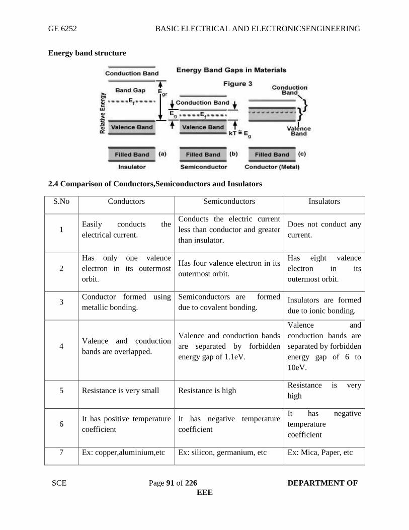
GE 6252 BASIC ELECTRICAL AND ELECTRONICSENGINEERING
SCE Page 91 of 226 DEPARTMENT OF
EEE
Energy band structure
2.4 Comparison of Conductors,Semiconductors and Insulators
S.No Conductors Semiconductors Insulators
1 Easily conducts the
electrical current.
Conducts the electric current
less than conductor and greater
than insulator.
Does not conduct any
current.
2
Has only one valence
electron in its outermost
orbit.
Has four valence electron in its
outermost orbit.
Has eight valence
electron in its
outermost orbit.
3 Conductor formed using
metallic bonding.
Semiconductors are formed
due to covalent bonding. Insulators are formed
due to ionic bonding.
4 Valence and conduction
bands are overlapped.
Valence and conduction bands
are separated by forbidden
energy gap of 1.1eV.
Valence and
conduction bands are
separated by forbidden
energy gap of 6 to
10eV.
5 Resistance is very small Resistance is high Resistance is very
high
6 It has positive temperature
coefficient
It has negative temperature
coefficient
It has negative
temperature
coefficient
7 Ex: copper,aluminium,etc Ex: silicon, germanium, etc Ex: Mica, Paper, etc

GE 6252 BASIC ELECTRICAL AND ELECTRONICSENGINEERING
SCE Page 92 of 226 DEPARTMENT OF
EEE
2.5 Classification of Semiconductor
Semiconductor
Intrinsic Semiconductor Extrinsic Semiconductor
2.6 Intrinsic Semiconductor
An intrinsic semiconductor also called an undoped semiconductor or i- type
semiconductor.
It is a pure semiconductor without any significant dopant species present.
The number of charge carriers determined by the properties of the m aterial itself instead
of the amount of impurities.
In intrinsic semiconductors the number of excited electrons and the number of holes are
equal: n = p.
Conductivity of Intrinsic semiconductor
The electrical conductivity of intrinsic semiconductors can be due to crystal defects
or to thermal excitation.
Both electrons and holes contribute to current flow in an intrinsic
semiconductor.

GE 6252 BASIC ELECTRICAL AND ELECTRONICSENGINEERING
SCE Page 93 of 226 DEPARTMENT OF
EEE
The current which will flow in an intrinsic semiconductor consists of both electron and
hole current.
That is, the electrons which have been freed from their lattice positions into the
conduction band can move through the material.
In addition, other electrons can hop between lattice positions to fill the vacancies left
by the freed electrons.
This additional mechanism is called hole conduction because it is as if the holes are
migrating across the material in the direction opposite to the free electron movement.
The current flow in an intrinsic semiconductor is influenced by the density of energy
states which in turn influences the electron density in the conduction band.
This current is highly temperature dependent.
Thermal excitation:
In an intrinsic semiconductor like silicon at temperatures above absolute zero, there
will be some electrons which are excited across the band gap into the conduction
band and which can produce current.
When the electron in pure silicon crosses the gap, it leaves behind an electron vacancy or
"hole" in the regular silicon lattice.
Under the influence of an external voltage, both the electron and the hole can move across
the material.
In n-type semiconductor:
The dopant contributes extra electrons, dramatically increasing the conductivity
In p-type semiconductor:
The dopant produces extra vacancies or holes, which likewise increase the
conductivity.
2.7 Extrinsic Semiconductor
The electrical conductivity of a pure semiconductor is very small. To increase the conductivity, impurities are added.
The impurity added semiconductor is called extrinsic semiconductor.
The process of adding impurity is called doping.
The added impurity is called dopant.
Usually one or two atoms of impurity is added per 106
atoms of a
semiconductor.
There are two types (i) p-type and (ii) n-type semiconductors.
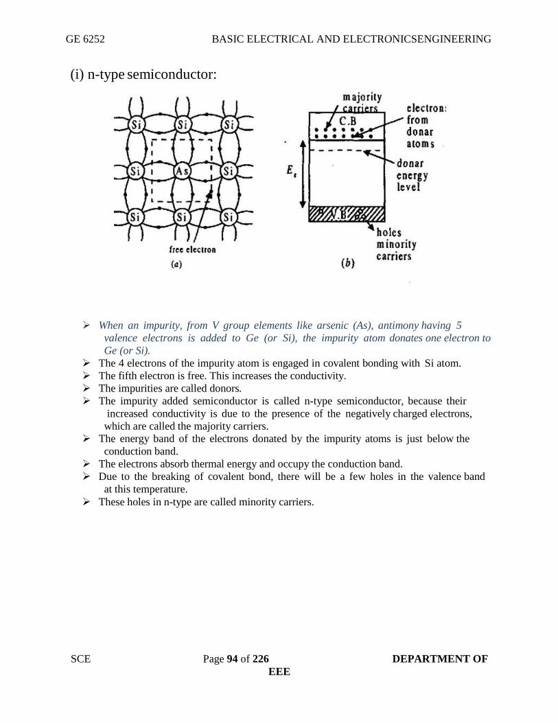
GE 6252 BASIC ELECTRICAL AND ELECTRONICSENGINEERING
SCE Page 94 of 226 DEPARTMENT OF
EEE
(i) n-type semiconductor:
When an impurity, from V group elements like arsenic (As), antimony having 5
valence electrons is added to Ge (or Si), the impurity atom donates one electron to
Ge (or Si).
The 4 electrons of the impurity atom is engaged in covalent bonding with Si atom.
The fifth electron is free. This increases the conductivity.
The impurities are called donors.
The impurity added semiconductor is called n-type semiconductor, because their
increased conductivity is due to the presence of the negatively charged electrons,
which are called the majority carriers.
The energy band of the electrons donated by the impurity atoms is just below the
conduction band.
The electrons absorb thermal energy and occupy the conduction band.
Due to the breaking of covalent bond, there will be a few holes in the valence band
at this temperature.
These holes in n-type are called minority carriers.
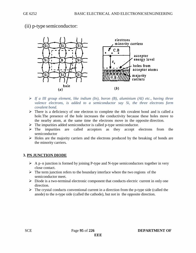
GE 6252 BASIC ELECTRICAL AND ELECTRONICSENGINEERING
SCE Page 95 of 226 DEPARTMENT OF
EEE
(ii) p-type semiconductor:
If a III group element, like indium (In), boron (B), aluminium (AI) etc., having three
valence electrons, is added to a semiconductor say Si, the three electrons form
covalent bond.
There is a deficiency of one electron to complete the 4th covalent bond and is called a
hole.The presence of the hole increases the conductivity because these holes move to
the nearby atom, at the same time the electrons move in the opposite direction.
The impurities added semiconductor is called p-type semiconductor.
The impurities are called acceptors as they accept electrons from the
semiconductor
Holes are the majority carriers and the electrons produced by the breaking of bonds are
the minority carriers.
3. PN JUNCTION DIODE
A p–n junction is formed by joining P-type and N-type semiconductors together in very
close contact.
The term junction refers to the boundary interface where the two regions of the
semiconductor meet.
Diode is a two-terminal electronic component that conducts electric current in only one
direction.
The crystal conducts conventional current in a direction from the p-type side (called the
anode) to the n-type side (called the cathode), but not in the opposite direction.

GE 6252 BASIC ELECTRICAL AND ELECTRONICSENGINEERING
SCE Page 96 of 226 DEPARTMENT OF
EEE
Symbol of PN junction diode
3.1Biasing
“Biasing” is providing minimum external voltage and current to activate the device to
study its characteristics.
There are two operating regions and two "biasing" conditions for the standard
Junction Diode and they are:
Zero Bias:
When a diode is Zero Biased no external energy source is applied and a natural Potential
Barrier is developed across a depletion layer.

GE 6252 BASIC ELECTRICAL AND ELECTRONICSENGINEERING
SCE Page 97 of 226 DEPARTMENT OF
EEE
(i) Forward Bias:
When the positive terminal of a battery is connected to P-type semiconductor and negative
terminal to N-type is known as forward bias of PN junction.
The applied forward potential establishes an electric field opposite to the potential barrier.
Therefore the potential barrier is reduced at the junction. As the potential barrier is very small
(0.3V for Ge and 0.7V for Si),a small forward voltage is sufficient to completely eliminate the
barrier potential, thus the junction resistance becomes zero.
In otherwords, the applied positive potential repels the holes in the ‘P’ region so that the holes
moves towards the junction and applied negative potential repels the electrons in the ‘N’ region
towards the junction results in depletion region starts decreasing. When the applied potential is
more than the internal barrier potential then the depletion region completely disappear, thus the
junction resistance becomes zero.
Once the potential barrier is eliminated by a forward voltage, j unction establishes the low
resistance path for the entire circuit, thus a current flows in the circuit, it is called as forward
current.
(ii)Reverse Bias:

GE 6252 BASIC ELECTRICAL AND ELECTRONICSENGINEERING
SCE Page 98 of 226 DEPARTMENT OF
EEE
For reverse bias, the negative terminal is connected to P-type semiconductor and positive terminal
to N type semiconductor.
When reverse bias voltage is applied to the junction, all the majority carriers of ‘P’ region are
attracted towards the negative terminal of the battery and the majority carriers of the N region
attracted towards the positive terminal of the battery, hence the depletion region increases.
The applied reverse voltage establishes an electric field which acts in the same direction of the
potential barrier. Therefore, the resultant field at the junction is strengthened and the barrier width
is increased. This increased potential barrier prevents the flow of charge carriers across the
junction, results in a high resistance path.
This process cannot continue indefinitely because after certain extent the junction break down
occurs. As a result a small amount of current flows through it due to minority carriers. This
current is known as “reverse saturation current”.
3.2 V-I characteristics of PN junction diode
Forward Bias:
The application of a forward biasing voltage on the junction diode results in the
depletion layer becoming very thin and narrow which represents a low impedance
path through the junction thereby allowing high currents to flow.
The point at which this sudden increase in current takes place is represented on the static
I-V characteristics curve above as the "knee" point.
Reverse Bias:
In Reverse biasing voltage a high resistance value to the PN junction and practically
zero current flows through the junction diode with an increase in bias voltage.
However, a very small leakage current does flow through the junction which can be
measured in microamperes, (μA).
One final point, if the reverse bias voltage Vr applied to the diode is increased to a
sufficiently high enough value, it will cause the PN junction to overheat and fail due to
the avalanche effect around the junction.
This may cause the diode to become shorted and will result in the flow of maximum
circuit current, and this shown as a step downward slope in the reverse static
characteristics curve below.

GE 6252 BASIC ELECTRICAL AND ELECTRONICSENGINEERING
SCE Page 99 of 226 DEPARTMENT OF
EEE
4. ZENER EFFECT
In a general purpose PN diode the doping is light; as a result of this the breakdown
voltage is high. If a P and N region are heavily doped then the breakdown voltage can be
reduced.
When the doping is heavy, even the reverse voltage is low, the electric field at barrier will
be so strong thus the electrons in the covalent bonds can break away from the bonds. This
effect is known as Zener effect.
5. ZENER DIODE
A diode which exhibits the zener effect is called a Zener Diode. Hence it is defined as a
reverse biased heavily doped PN junction diode which operates in breakdown region. The
zener diodes have been designed to operate at voltages ranging from a few volts to
several hundred volts.
Zener Breakdown occurs in junctions which is heavily doped and have narrow depletion
layers. The breakdown voltage sets up a very strong electric field. This field is so strong
enough to break or rupture the covalent bonds thereby generating electron hole pairs.

GE 6252 BASIC ELECTRICAL AND ELECTRONICSENGINEERING
SCE Page 100 of 226 DEPARTMENT OF
EEE
Even a small reverse voltage is capable of producing large number of current carrier.
When a zener diode is operated in the breakdown region care must be taken to see that
the power dissipation across the junction is within the power rating of the diode otherwise
heavy current flowing through the diode may destroy it.
5.1 V-I characteristics of Zener diode
The illustration above shows this phenomenon in a current vs voltage graph with a
zener diode connected in the forward direction .It behaves exactly as a standard diode.
In the reverse direction however there is a very small leakage current between 0v
and the zener voltage –i.e. just a tiny amount of current is able to flow.
Then, when the voltage reaches the breakdown voltage (vz),suddenly current can flow
freely through it.
5.2 Application of Zener diode
a) as voltage regulator
b) as peak clippers
c) for reshaping waveforms

GE 6252 BASIC ELECTRICAL AND ELECTRONICSENGINEERING
SCE Page 101 of 226 DEPARTMENT OF
EEE
6. RECTIFIERS
The “rectifier” is a circuit that converts AC voltages and currents into pulsating DC
voltages and currents. It consists of DC components and the unwanted ac ripple or harmonic
components which can be removed by using filter circuit. Thus the output obtained will be
steady DC voltage and magnitude of DC voltage can be varied by varying the magnitude of AC
voltage.
Filters: A circuit that removes ripples (unwanted ac components) present in the pulsating
dc voltage.
Regulator: A circuit that maintains the terminal voltage as constant even if the input
voltage or load current varying.
6.1 Types of rectifiers:
Rectifiers are grouped into two categories depending on the period of conduction.
(a)Half wave rectifier (b) Full wave rectifier
Half wave Rectifier:
Principle
It is a circuit that converts alternating voltage or current into pulsating voltage or current
for half the period of input cycle hence it is named as “half wave rectifier”.
Construction
It consists of step-down transformer, semiconductor diode and the load resistance.
The step-down transformer – reduce the available ac voltage into required level of
smaller ac voltage.
The diode can be used to convert the ac into pulsating dc.
Operation
During the positive half cycle of input, the diode D is forward biased, it offers very small
resistance and it acts as closed switch and hence conducts the current through the load
resistor.
During the negative half cycle of the input diode D is heavily reverse biased, it offers
very high resistance and it acts as open switch hence it does not conduct any current. The
rectified output voltage will be in phase with AC input voltage for completely resistive
load.

GE 6252 BASIC ELECTRICAL AND ELECTRONICSENGINEERING
SCE Page 102 of 226 DEPARTMENT OF
EEE
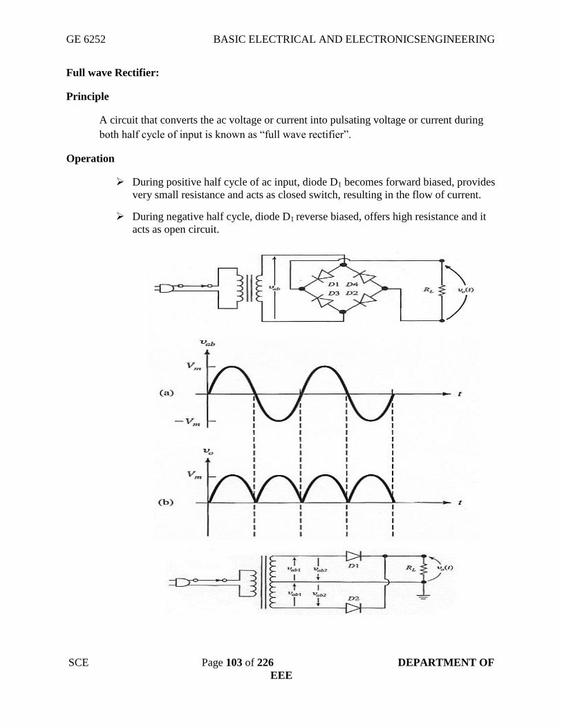
GE 6252 BASIC ELECTRICAL AND ELECTRONICSENGINEERING
SCE Page 103 of 226 DEPARTMENT OF
EEE
Full wave Rectifier:
Principle
A circuit that converts the ac voltage or current into pulsating voltage or current during
both half cycle of input is known as “full wave rectifier”.
Operation
During positive half cycle of ac input, diode D1 becomes forward biased, provides
very small resistance and acts as closed switch, resulting in the flow of current.
During negative half cycle, diode D1 reverse biased, offers high resistance and it
acts as open circuit.

GE 6252 BASIC ELECTRICAL AND ELECTRONICSENGINEERING
SCE Page 104 of 226 DEPARTMENT OF
EEE
Voltage Regulation:
Ratio of Difference of secondary voltage to Primary voltage to secondary
voltage.
7. BIPOLAR JUNCTION TRANSISTOR
A bipolar junction transistor is a three terminal semiconductor device in which the
operation depends on the interaction of majority and minority carriers.
Transistor refers to Transfer Resistor i.e., signals are transferred from low resistance
circuit into high resistance circuit.
BJT consists of silicon crystal in which a layer of ‘N’ type silicon is sandwiched between
two layers of ‘P’ type silicon. The semiconductor sandwiched is extremely smaller in
size.
In other words, it consists of two back to back PN junction joined together to form single
piece of semiconductor crystal. These two junctions gives three region called Emitter,
Base and Collector.
There are two types of transistors such as PNP and NPN. The arrow on the emitter
specifies whether the transistor is PNP or NPN type and also determines the direction of
flow of current, when the emitter base junction is forward biased.
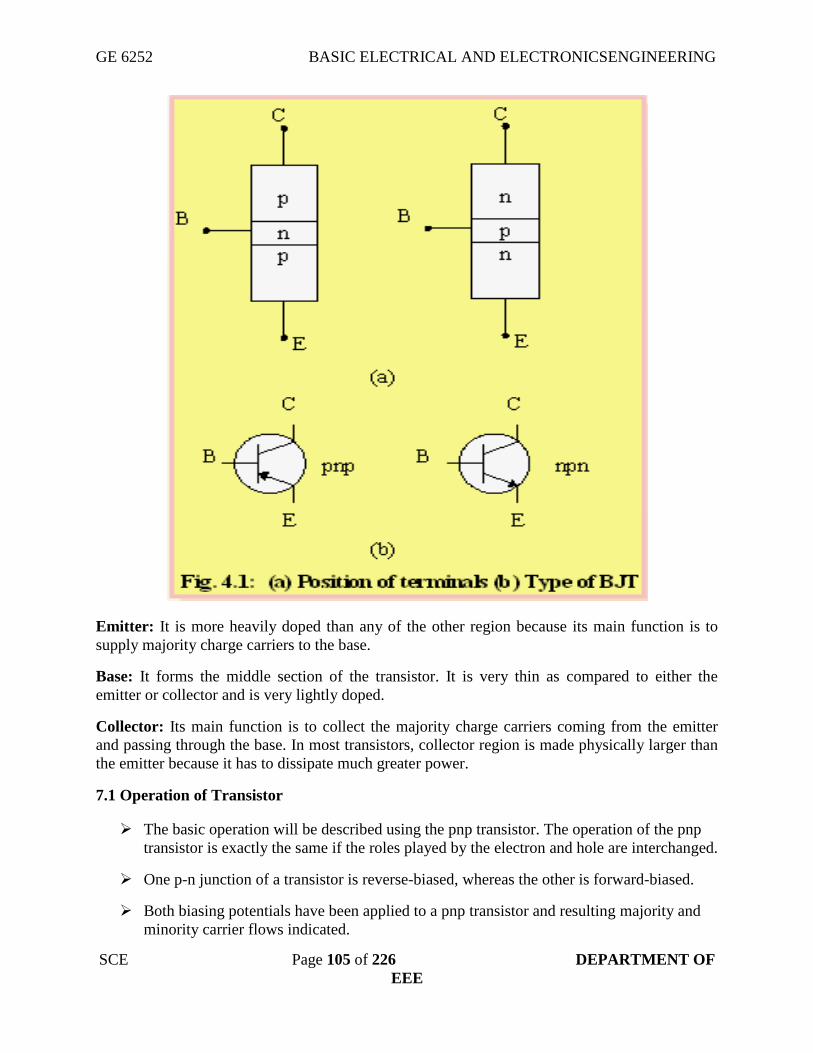
GE 6252 BASIC ELECTRICAL AND ELECTRONICSENGINEERING
SCE Page 105 of 226 DEPARTMENT OF
EEE
Emitter: It is more heavily doped than any of the other region because its main function is to
supply majority charge carriers to the base.
Base: It forms the middle section of the transistor. It is very thin as compared to either the
emitter or collector and is very lightly doped.
Collector: Its main function is to collect the majority charge carriers coming from the emitter
and passing through the base. In most transistors, collector region is made physically larger than
the emitter because it has to dissipate much greater power.
7.1 Operation of Transistor
The basic operation will be described using the pnp transistor. The operation of the pnp
transistor is exactly the same if the roles played by the electron and hole are interchanged.
One p-n junction of a transistor is reverse-biased, whereas the other is forward-biased.
Both biasing potentials have been applied to a pnp transistor and resulting majority and
minority carrier flows indicated.

GE 6252 BASIC ELECTRICAL AND ELECTRONICSENGINEERING
SCE Page 106 of 226 DEPARTMENT OF
EEE
Forward biased junction of a pnp transistor
Reverse biased junction of pnp transistor
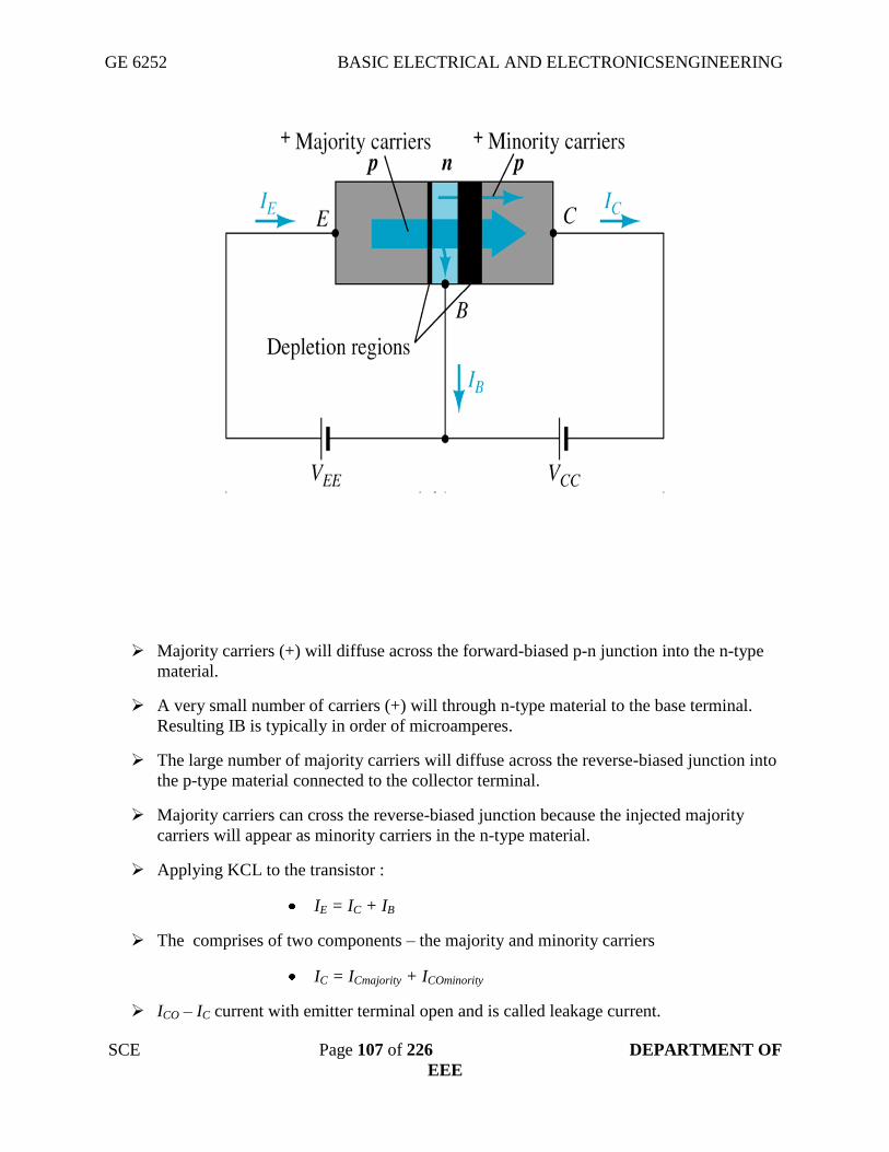
GE 6252 BASIC ELECTRICAL AND ELECTRONICSENGINEERING
SCE Page 107 of 226 DEPARTMENT OF
EEE
Majority carriers (+) will diffuse across the forward-biased p-n junction into the n-type
material.
A very small number of carriers (+) will through n-type material to the base terminal.
Resulting IB is typically in order of microamperes.
The large number of majority carriers will diffuse across the reverse-biased junction into
the p-type material connected to the collector terminal.
Majority carriers can cross the reverse-biased junction because the injected majority
carriers will appear as minority carriers in the n-type material.
Applying KCL to the transistor :
IE = IC + IB
The comprises of two components – the majority and minority carriers
IC = ICmajority + ICOminority
ICO – IC current with emitter terminal open and is called leakage current.
GE 6252 BASIC ELECTRICAL AND ELECTRONICSENGINEERING
SCE Page 108 of 226 DEPARTMENT OF
EEE
7.2 Common Base configuration
Common-base terminology is derived from the fact that the :
- base is common to both input and output of the configuration.
- base is usually the terminal closest to or at ground potential.
All current directions will refer to conventional (hole) flow and the arrows in all
electronic symbols have a direction defined by this convention.
Note that the applied biasing (voltage sources) are such as to establish current in the
direction indicated for each branch.
To describe the behavior of common-base amplifiers requires two set of characteristics:
o Input or driving point characteristics.
o Output or collector characteristics
The output characteristics has 3 basic regions:
o Active region –defined by the biasing arrangements
o Cutoff region – region where the collector current is 0A

GE 6252 BASIC ELECTRICAL AND ELECTRONICSENGINEERING
SCE Page 109 of 226 DEPARTMENT OF
EEE
o Saturation region- region of the characteristics to the left of VCB = 0V
GE 6252 BASIC ELECTRICAL AND ELECTRONICSENGINEERING
SCE Page 110 of 226 DEPARTMENT OF
EEE
The curves (output characteristics) clearly indicate that a first approximation to the
relationship between IE and IC in the active region is given by
IC ≈IE
Once a transistor is in the ‘on’ state, the base-emitter voltage will be assumed to be
VBE = 0.7V
In the dc mode the level of IC and IE due to the majority carriers are related by a quantity
called alpha

GE 6252 BASIC ELECTRICAL AND ELECTRONICSENGINEERING
SCE Page 111 of 226 DEPARTMENT OF
EEE
= IC / IE
IC = IE + ICBO
It can then be summarize to IC = IE (ignore ICBO due to small value)
For ac situations where the point of operation moves on the characteristics curve, an ac
alpha defined by
Alpha a common base current gain factor that shows the efficiency by calculating the
current percent from current flow from emitter to collector. The value of is typical from
0.9 ~ 0.998.
7.3 Common Emitter configuration
It is called common-emitter configuration since :
o emitter is common or reference to both input and output terminals.
o emitter is usually the terminal closest to or at ground potential.
Almost amplifier design is using connection of CE due to the high gain for current and
voltage.
Two set of characteristics are necessary to describe the behavior for CE; input (base
terminal) and output (collector terminal) parameters.
GE 6252 BASIC ELECTRICAL AND ELECTRONICSENGINEERING
SCE Page 112 of 226 DEPARTMENT OF
EEE

GE 6252 BASIC ELECTRICAL AND ELECTRONICSENGINEERING
SCE Page 113 of 226 DEPARTMENT OF
EEE
Input characteristics for CE configuration
IB in microamperes compared to milliamperes of IC.
IB will flow when VBE > 0.7V for silicon and 0.3V for germanium
Before this value IB is very small and no IB.
Base-emitter junction is forward bias
Increasing VCE will reduce IB for different values.

GE 6252 BASIC ELECTRICAL AND ELECTRONICSENGINEERING
SCE Page 114 of 226 DEPARTMENT OF
EEE
Output characteristics for CE configuration
For small VCE (VCE < VCESAT, IC increase linearly with increasing of VCE
VCE > VCESAT IC not totally depends on VCE constant IC
IB(uA) is very small compare to IC (mA). Small increase in IB cause big increase in IC
IB=0 A ICEO occur.
Noticing the value when IC=0A. There is still some value of current flows.
GE 6252 BASIC ELECTRICAL AND ELECTRONICSENGINEERING
SCE Page 115 of 226 DEPARTMENT OF
EEE
7.4 Common Collector configuration
Also called emitter-follower (EF).
It is called common-emitter configuration since both the
o signal source and the load share the collector terminal as a common connection
point.
The output voltage is obtained at emitter terminal.
The input characteristic of common-collector configuration is similar with common-
emitter. configuration.
Common-collector circuit configuration is provided with the load resistor connected from
emitter to ground.

GE 6252 BASIC ELECTRICAL AND ELECTRONICSENGINEERING
SCE Page 116 of 226 DEPARTMENT OF
EEE
It is used primarily for impedance-matching purpose since it has high input impedance
and low output impedance.
For the common-collector configuration, the output characteristics are a plot of IE
vs VCE for a range of values of IB.
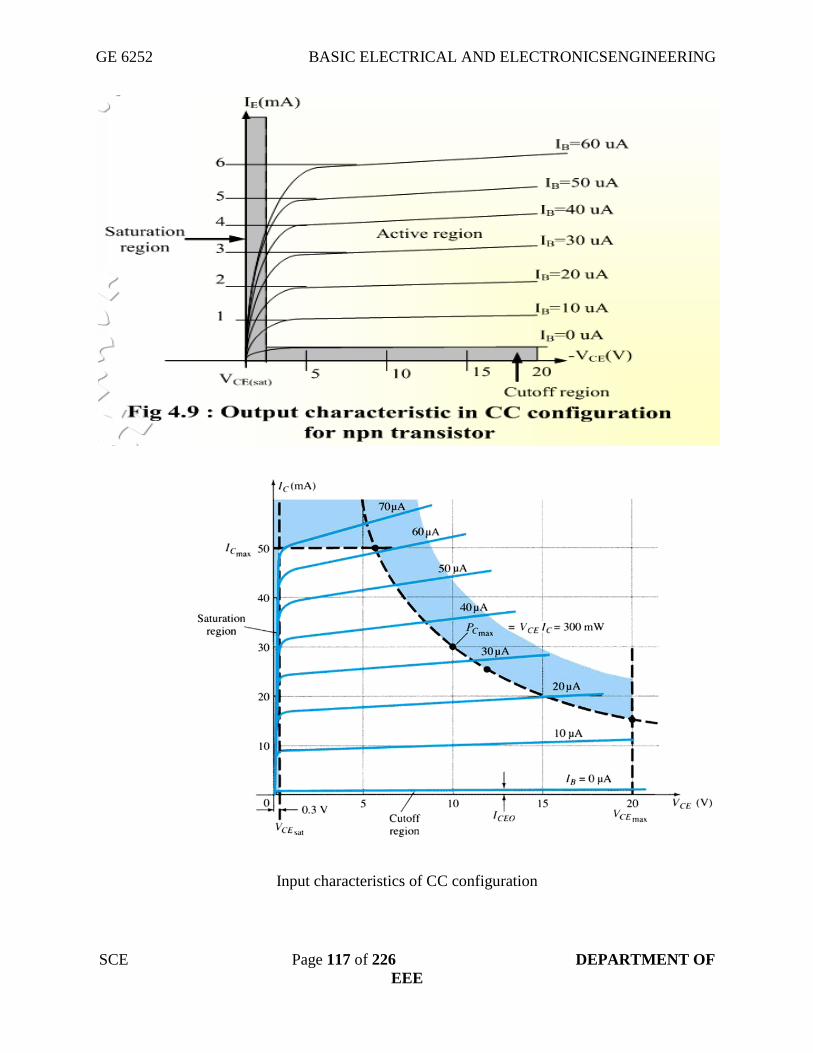
GE 6252 BASIC ELECTRICAL AND ELECTRONICSENGINEERING
SCE Page 117 of 226 DEPARTMENT OF
EEE
Input characteristics of CC configuration
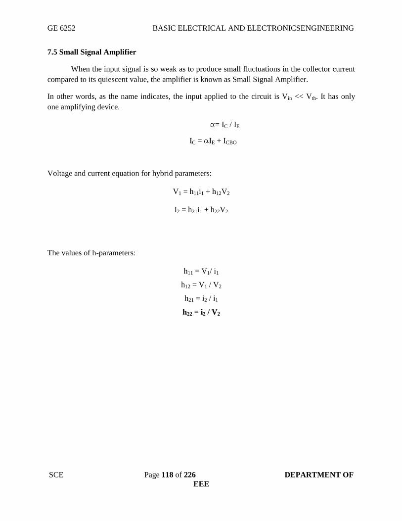
GE 6252 BASIC ELECTRICAL AND ELECTRONICSENGINEERING
SCE Page 118 of 226 DEPARTMENT OF
EEE
7.5 Small Signal Amplifier
When the input signal is so weak as to produce small fluctuations in the collector current
compared to its quiescent value, the amplifier is known as Small Signal Amplifier.
In other words, as the name indicates, the input applied to the circuit is Vin << Vth. It has only
one amplifying device.
= IC / IE
IC = IE + ICBO
Voltage and current equation for hybrid parameters:
V1 = h11i1 + h12V2
I2 = h21i1 + h22V2
The values of h-parameters:
h11 = V1/ i1
h12 = V1 / V2
h21 = i2 / i1
h22 = i2 / V2

GE 6252 BASIC ELECTRICAL AND ELECTRONICSENGINEERING
SCE Page 119 of 226 DEPARTMENT OF
EEE
UNIT-IV DIGITAL ELECTRONICS
4.1 BINARY NUMBER SYSTEM
4.1.1.1 Introduction
The number system that you are familiar with, that you use every day, is the decimal
number system, also commonly referred to as the base-10 system. When you perform
computations such as 3 + 2 = 5, or 21 – 7 = 14, you are using the decimal number system. This
system, which you likely learned in first or second grade, is ingrained into your subconscious;
it’s the natural way that you think about numbers. Evidence exists that Egyptians were using a
decimal number system five thousand years ago. The Roman numeral system, predominant for
hundreds of years, was also a decimal number system (though organized differently from the
Arabic base-10 number system that we are most familiar with). Indeed, base-10 systems, in one
form or another, have been the most widely used number systems ever since civilization started
counting.
In dealing with the inner workings of a computer, though, you are going to have to learn
to think in a different number system, the binary number system, also referred to as the base-2
system.
Consider a child counting a pile of pennies. He would begin: “One, two, three, …, eight,
nine.” Upon reaching nine, the next penny counted makes the total one single group of ten
pennies. He then keeps counting: “One group of ten pennies… two groups of ten pennies… three
groups of ten pennies … eight groups of ten pennies … nine groups of ten pennies…” Upon
reaching nine groups of ten pennies plus nine additional pennies, the next penny counted makes
the total thus far: one single group of one hundred pennies. Upon completing the task, the child
might find that he has three groups of one hundred pennies, five groups of ten pennies, and two
pennies left over: 352 pennies.
More formally, the base-10 system is a positional system, where the rightmost digit is the
ones position (the number of ones), the next digit to the left is the tens position (the number of
groups of 10), the next digit to the left is the hundreds position (the number of groups of 100),
and so forth. The base-10 number system has 10 distinct symbols, or digits (0, 1, 2, 3,…8, 9). In
decimal notation, we write a number as a string of symbols, where each symbol is one of these
ten digits, and to interpret a decimal number, we multiply each digit by the power of 10
associated with that digit’s position.
For example, consider the decimal number: 6349. This number is:
6 3 4 9 = 6 ⋅103 + 3 ⋅10
2 + 4 ⋅101 + 9 ⋅10
0
103
10
2 10
1 10
0
position position position position
(i.e., thousands position) (i.e., hundreds position) (i.e., tens position) (i.e., ones position)

GE 6252 BASIC ELECTRICAL AND ELECTRONICSENGINEERING
SCE Page 120 of 226 DEPARTMENT OF
EEE
Consider: Computers are built from transistors, and an individual transistor can only be
ON or OFF (two options). Similarly, data storage devices can be optical or magnetic. Optical
storage devices store data in a specific location by controlling whether light is reflected off that
location or is not reflected off that location (two options). Likewise, magnetic storage devices
store data in a specific location by magnetizing the particles in that location with a specific
orientation. We can have the north magnetic pole pointing in one direction, or the opposite
direction (two options).
Computers can most readily use two symbols, and therefore a base-2 system, or binary
number system, is most appropriate. The base-10 number system has 10 distinct symbols: 0, 1, 2,
3, 4, 5, 6, 7, 8 and 9. The base-2 system has exactly two symbols: 0 and 1. The base-10 symbols
are termed digits. The base-2 symbols are termed binary digits, or bits for short. All base-10
numbers are built as strings of digits (such as 6349). All binary numbers are built as strings of
bits (such as 1101). Just as we would say that the decimal number 12890 has five digits, we
would say that the binary number 11001 is a five-bit number.
1.2 The Binary Number System
Consider again the example of a child counting a pile of pennies, but this time in binary.
He would begin with the first penny: “1.” The next penny counted makes the total one single
group of two pennies. What number is this?
When the base-10 child reached nine (the highest symbol in his scheme), the next penny
gave him “one group of ten”, denoted as 10, where the “1” indicated one collection of ten.
Similarly, when the base-2 child reaches one (the highest symbol in his scheme), the next penny
gives him “one group of two”, denoted as 10, where the “1” indicates one collection of two.
Back to the base-2 child: The next penny makes one group of two pennies and one
additional penny: “11.” The next penny added makes two groups of two, which is one group of
4: “100.” The “1” here indicates a collection of two groups of two, just as the “1” in the base-10
number 100 indicates ten groups of ten.
Upon completing the counting task, base -2 child might find that he has one group of four
pennies, no groups of two pennies, and one penny left over: 101 pennies. The child counting the
same pile of pennies in base-10 would conclude that there were 5 pennies. So, 5 in base-10 is
equivalent to 101 in base-2. To avoid confusion when the base in use if not clear from the
context, or when using multiple bases in a single expression, we append a subscript to the
number to indicate the base, and write:
510 =1012
Just as with decimal notation, we write a binary number as a string of symbols, but now
each symbol is a 0 or a 1. To interpret a binary number, we multiply each digit by the power of
2 associated with that digit’s position.
For example, consider the binary number 1101. This number is:

GE 6252 BASIC ELECTRICAL AND ELECTRONICSENGINEERING
SCE Page 121 of 226 DEPARTMENT OF
EEE
1 1 0 1 = 1⋅ 2 3 + 1 ⋅ 2 2 + 0 ⋅ 21 + 1 ⋅ 2 0 = 1310
23 2
2 2
1 2
0
position position position position
(i.e., eights position) (i.e., fours position) (i.e., twos position) (i.e., ones position)
Since binary numbers can only contain the two symbols 0 and 1, numbers such as 25 and
1114000 cannot be binary numbers.
We say that all data in a computer is stored in binary—that is, as 1’s and 0’s. It is
important to keep in mind that values of 0 and 1 are logical values, not the values of a physical
quantity, such as a voltage. The actual physical binary values used to store data internally within
a computer might be, for instance, 5 volts and 0 volts, or perhaps 3.3 volts and 0.3 volts or
perhaps reflection and no reflection. The two values that are used to physically store data can
differ within different portions of the same computer. All that really matters is that there are two
different symbols, so we will always refer to them as 0 and 1.
A string of eight bits (such as 11000110) is termed a byte. A collection of four bits (such
as 1011) is smaller than a byte, and is hence termed a nibble. (This is the sort of nerd-humor for
which engineers are famous.)
The idea of describing numbers using a positional system, as we have illustrated for base-
10 and base-2, can be extended to any base. For example, the base-4 number 231 is:
2 3 1 = 2 ⋅ 4 2 + 3 ⋅ 41 + 1 ⋅ 4 0 = 4510
42 4
1 4
0
position position position
(i.e., sixteens position) (i.e., fours position) (i.e., ones position)
1.3 Converting Between Binary Numbers and Decimal Numbers
We humans about numbers using the decimal number system, whereas computers use the
binary number system. We need to be able to readily shift between the binary and decimal
number representations.

GE 6252 BASIC ELECTRICAL AND ELECTRONICSENGINEERING
SCE Page 122 of 226 DEPARTMENT OF
EEE
Converting a Binary Number to a Decimal Number
To convert a binary number to a decimal number, we simply write the binary number as a
sum of powers of 2. For example, to convert the binary number 1011 to a decimal number, we
note that the rightmost position is the ones position and the bit value in this position is a 1. So,
this rightmost bit has the decimal value of 1⋅20 . The next position to the left is the twos
position, and the bit value in this position is also a 1. So, this next bit has the decimal value of 1⋅
21 . The next position to the left is the fours position, and the bit value in this position is a 0.
The leftmost position is the eights position, and the bit value in this position is a 1. So, this
leftmost bit has the decimal value of 1⋅23 . Thus:
1011 = 1 ⋅ 2 3 + 0 ⋅ 2
2 + 1 ⋅ 21
+ 1 ⋅ 2 0 = 8 + 2 + 1 = 11
2 10 1. The binary number 110110 as a decimal number.
Solution:
For example, to convert the binary number 10101 to decimal, we annotate the position
values below the bit values:
1 0 1 0 1
16 8 4 2 1
Then we add the position values for those positions that have a bit value of 1: 16 + 4 + 1
= 21. Thus
101012 = 2110
You should “memorize” the binary representations of the decimal digits 0 through 15
shown below.
Decimal Number Binary Number
Decimal Number Binary Number
0 0000 8 1000
1 0001 9 1001
2 0010 10 1010
3 0011 11 1011
4 0100 12 1100
5 0101 13 1101
6 0110 14 1110
7 0111 15 1111
You may be wondering about the leading zeros in the table above. For example, the
decimal number 5 is represented in the table as the binary number 0101. We could have
represented the binary equivalent of 5 as 101, 00101, 0000000101, or with any other number of
leading zeros. All answers are correct.
Sometimes, though, you will be given the size of a storage location. When you are given

GE 6252 BASIC ELECTRICAL AND ELECTRONICSENGINEERING
SCE Page 123 of 226 DEPARTMENT OF
EEE
the size of the storage location, include the leading zeros to show all bits in the storage location.
For example, if told to represent decimal 5 as an 8-bit binary number, your answer should be
00000101. Converting a Decimal Number to a Binary Number: Method 2
The second method of converting a decimal number to a binary number entails repeatedly
dividing the decimal number by 2, keeping track of the remainder at each step. To convert the
decimal number x to binary:
Step 1. Divide x by 2 to obtain a quotient and remainder. The remainder will be 0 or 1.
Step 2. If the quotient is zero, you are finished: Proceed to Step 3. Otherwise, go back to
Step 1, assigning x to be the value of the most-recent quotient from Step 1.
Step 3. The sequence of remainders forms the binary representation of the number.
1.4 Hexadecimal Numbers
In addition to binary, another number base that is commonly used in digital systems is
base 16. This number system is called hexadecimal, and each digit position represents a power of
16. For any number base greater than ten, a problem occurs because there are more than ten
symbols needed to represent the numerals for that number base. It is customary in these cases to
use the ten decimal numerals followed by the letters of the alphabet beginning with A to provide
the needed numerals. Since the hexadecimal system is base 16, there are sixteen numerals
required. The following are the hexadecimal numerals:
0, 1, 2, 3, 4, 5, 6, 7, 8, 9, A, B, C, D, E, F
The following are some examples of hexadecimal numbers:
1016 4716 3FA16 A03F16
The reason for the common use of hexadecimal numbers is the relationship between the
numbers 2 and 16. Sixteen is a power of 2 (16 = 24). Because of this relationship, four digits in a
binary number can be represented with a single hexadecimal digit. This makes conversion
between binary and hexadecimal numbers very easy, and hexadecimal can be used to write large
binary numbers with much fewer digits. When working with large digital systems, such as
computers, it is common to find binary numbers with 8, 16 and even 32 digits. Writing a 16 or 32
bit binary number would be quite tedious and error prone. By using hexadecimal, the numbers
can be written with fewer digits and much less likelihood of error.
To convert a binary number to hexadecimal, divide it into groups of four digits starting with the
rightmost digit. If the number of digits isn’t a multiple of 4, prefix the number with 0’s so that
each group contains 4 digits. For each four digit group, convert the 4 bit binary number into an
equivalent hexadecimal digit. (See the Binary, BCD, and Hexadecimal Number Tables at the end

GE 6252 BASIC ELECTRICAL AND ELECTRONICSENGINEERING
SCE Page 124 of 226 DEPARTMENT OF
EEE
of this document for the correspondence between 4 bit binary patterns and hexadecimal digits)
2. Convert the binary number 10110101 to a hexadecimal number
Divide into groups for 4 digits 1011 0101
Convert each group to hex digit B 5
B516
3. Convert the binary number 0110101110001100 to hexadecimal
Divide into groups of 4 digits 0110 1011 1000 1100
Convert each group to hex digit 6 B 8 C
6B8C16
To convert a hexadecimal number to a binary number, convert each hexadecimal
digit into a group of 4 binary digits.
4. Convert the hex number 374F into binary
3 7 4 F Convert the hex digits to binary 0011 0111 0100 1111
00110111010011112
There are several ways in common use to specify that a given number is in hexadecimal
representation rather than some other radix. In cases where the context makes it absolutely clear
that numbers are represented in hexadecimal, no indicator is used. In much written material
where the context doesn’t make it clear what the radix is, the numeric subscript 16 following the
hexadecimal number is used. In most programming languages, this method isn’t really feasible,
so there are several conventions used depending on the language. In the C and C++ languages,
hexadecimal constants are represented with a ‘0x’ preceding the number, as in: 0x317F, or
0x1234, or 0xAF. In assembler programming languages that follow the Intel style, a hexadecimal
constant begins with a numeric character (so that the assembler can distinguish it from a variable
name), a leading ‘0’ being used if necessary. The letter ‘h’ is then suffixed onto the number to
inform the assembler that it is a hexadecimal constant. In Intel style assembler format: 371Fh and
0FABCh are valid hexadecimal constants. Note that: A37h isn’t a valid hexadecimal constant. It
doesn’t begin with a numeric character, and so will be taken by the assembler as a variable name.
In assembler programming languages that follow the Motorola style, hexadecimal constants
begin with a ‘$’ character. So in this case: $371F or $FABC or $01 are valid hexadecimal
constants.
1.5 Binary Coded Decimal Numbers
Another number system that is encountered occasionally is Binary Coded Decimal.
In this system, numbers are represented in a decimal form, however each decimal digit is
encoded using a four bit binary number.
5. The decimal number 136 would be represented in BCD as follows:
136 = 0001 0011 0110

GE 6252 BASIC ELECTRICAL AND ELECTRONICSENGINEERING
SCE Page 125 of 226 DEPARTMENT OF
EEE
1 3 6
Conversion of numbers between decimal and BCD is quite simple. To convert from
decimal to BCD, simply write down the four bit binary pattern for each decimal digit. To convert
from BCD to decimal, divide the number into groups of 4 bits and write down the corresponding
decimal digit for each 4 bit group.
There are a couple of variations on the BCD representation, namely packed and
unpacked. An unpacked BCD number has only a single decimal digit stored in each data byte.
In this case, the decimal digit will be in the low four bits and the upper 4 bits of the byte will be
0. In the packed BCD representation, two decimal digits are placed in each byte. Generally, the
high order bits of the data byte contain the more significant decimal digit.
6. The following is a 16 bit number encoded in packed BCD format: 01010110 10010011
This is converted to a decimal number as follows:
0101 0110 1001 0011 5 6 9 3
The value is 5693 decimal
7. The same number in unpacked BCD (requires 32 bits) 00000101 00000110 00001001 00000011
5 6 9 3
The use of BCD to represent numbers isn’t as common as binary in most computer
systems, as it is not as space efficient. In packed BCD, only 10 of the 16 possible bit patterns in
each 4 bit unit are used. In unpacked BCD, only 10 of the 256 possible bit patterns in each byte
are used. A 16 bit quantity can represent the range 0-65535 in binary, 0-9999 in packed BCD and
only 0-99 in unpacked BCD. Fixed Precision and Overflow
we haven’t considered the maximum size of the number. We have assumed that as many
bits are available as needed to represent the number. In most computer systems, this isn’t the
case. Numbers in computers are typically represented using a fixed number of bits. These sizes
are typically 8 bits, 16 bits, 32 bits, 64 bits and 80 bits. These sizes are generally a multiple of 8,
as most computer memories are organized on an 8 bit byte basis. Numbers in which a specific
number of bits are used to represent the value are called fixed precision numbers. When a
specific number of bits are used to represent a number, that determines the range of possible
values that can be represented. For example, there are 256 possible combinations of 8 bits,
therefore an 8 bit number can represent 256 distinct numeric values and the range is typically
considered to be 0-255. Any number larger than 255 can’t be represented using 8 bits. Similarly,
16 bits allows a range of 0-65535.
When fixed precision numbers are used, (as they are in virtually all computer
calculations) the concept of overflow must be considered. An overflow occurs when the result of
a calculation can’t be represented with the number of bits available. For example when adding
the two eight bit quantities: 150 + 170, the result is 320. This is outside the range 0-255, and so
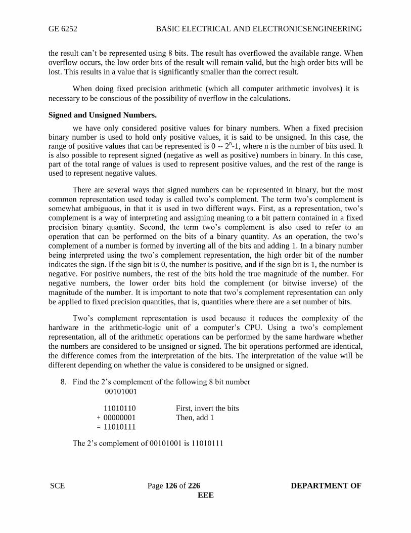
GE 6252 BASIC ELECTRICAL AND ELECTRONICSENGINEERING
SCE Page 126 of 226 DEPARTMENT OF
EEE
the result can’t be represented using 8 bits. The result has overflowed the available range. When
overflow occurs, the low order bits of the result will remain valid, but the high order bits will be
lost. This results in a value that is significantly smaller than the correct result.
When doing fixed precision arithmetic (which all computer arithmetic involves) it is
necessary to be conscious of the possibility of overflow in the calculations. Signed and Unsigned Numbers.
we have only considered positive values for binary numbers. When a fixed precision binary number is used to hold only positive values, it is said to be unsigned. In this case, the range of positive values that can be represented is 0 -- 2
n-1, where n is the number of bits used. It
is also possible to represent signed (negative as well as positive) numbers in binary. In this case, part of the total range of values is used to represent positive values, and the rest of the range is used to represent negative values.
There are several ways that signed numbers can be represented in binary, but the most
common representation used today is called two’s complement. The term two’s complement is
somewhat ambiguous, in that it is used in two different ways. First, as a representation, two’s
complement is a way of interpreting and assigning meaning to a bit pattern contained in a fixed
precision binary quantity. Second, the term two’s complement is also used to refer to an
operation that can be performed on the bits of a binary quantity. As an operation, the two’s
complement of a number is formed by inverting all of the bits and adding 1. In a binary number
being interpreted using the two’s complement representation, the high order bit of the number
indicates the sign. If the sign bit is 0, the number is positive, and if the sign bit is 1, the number is
negative. For positive numbers, the rest of the bits hold the true magnitude of the number. For
negative numbers, the lower order bits hold the complement (or bitwise inverse) of the
magnitude of the number. It is important to note that two’s complement representation can only
be applied to fixed precision quantities, that is, quantities where there are a set number of bits.
Two’s complement representation is used because it reduces the complexity of the
hardware in the arithmetic-logic unit of a computer’s CPU. Using a two’s complement
representation, all of the arithmetic operations can be performed by the same hardware whether
the numbers are considered to be unsigned or signed. The bit operations performed are identical,
the difference comes from the interpretation of the bits. The interpretation of the value will be
different depending on whether the value is considered to be unsigned or signed.
8. Find the 2’s complement of the following 8 bit number 00101001
11010110 First, invert the bits
+ 00000001 Then, add 1
= 11010111
The 2’s complement of 00101001 is 11010111
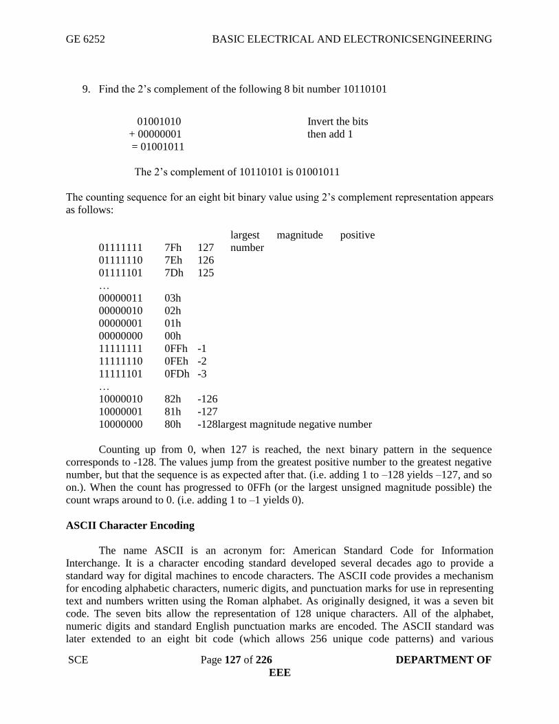
GE 6252 BASIC ELECTRICAL AND ELECTRONICSENGINEERING
SCE Page 127 of 226 DEPARTMENT OF
EEE
9. Find the 2’s complement of the following 8 bit number 10110101
01001010 Invert the bits
+ 00000001 then add 1
= 01001011
The 2’s complement of 10110101 is 01001011
The counting sequence for an eight bit binary value using 2’s complement representation appears
as follows:
01111111 7Fh 127
largest magnitude positive
number
01111110 7Eh 126
01111101 7Dh 125
…
00000011 03h
00000010 02h
00000001 01h
00000000 00h
11111111 0FFh -1
11111110 0FEh -2
11111101 0FDh -3
…
10000010 82h -126
10000001 81h -127
10000000 80h -128largest magnitude negative number
Counting up from 0, when 127 is reached, the next binary pattern in the sequence
corresponds to -128. The values jump from the greatest positive number to the greatest negative
number, but that the sequence is as expected after that. (i.e. adding 1 to –128 yields –127, and so
on.). When the count has progressed to 0FFh (or the largest unsigned magnitude possible) the
count wraps around to 0. (i.e. adding 1 to –1 yields 0).
ASCII Character Encoding
The name ASCII is an acronym for: American Standard Code for Information
Interchange. It is a character encoding standard developed several decades ago to provide a
standard way for digital machines to encode characters. The ASCII code provides a mechanism
for encoding alphabetic characters, numeric digits, and punctuation marks for use in representing
text and numbers written using the Roman alphabet. As originally designed, it was a seven bit
code. The seven bits allow the representation of 128 unique characters. All of the alphabet,
numeric digits and standard English punctuation marks are encoded. The ASCII standard was
later extended to an eight bit code (which allows 256 unique code patterns) and various

GE 6252 BASIC ELECTRICAL AND ELECTRONICSENGINEERING
SCE Page 128 of 226 DEPARTMENT OF
EEE
additional symbols were added, including characters with diacritical marks (such as accents)
used in European languages, which don’t appear in English. There are also numerous non-
standard extensions to ASCII giving different encoding for the upper 128 character codes than
the standard. For example, The character set encoded into the display card for the original IBM
PC had a non-standard encoding for the upper character set. This is a non-standard extension that
is in very wide spread use, and could be considered a standard in itself.
Some important things to points about ASCII code:
The numeric digits, 0-9, are encoded in sequence starting at 30h
The upper case alphabetic characters are sequential beginning at 41h
The lower case alphabetic characters are sequential beginning at 61h
The first 32 characters (codes 0-1Fh) and 7Fh are control characters. They do not
have a standard symbol (glyph) associated with them. They are used for carriage
control, and protocol purposes. They include 0Dh (CR or carriage return), 0Ah (LF or
line feed), 0Ch (FF or form feed), 08h (BS or backspace).
Most keyboards generate the control characters by holding down a control key
(CTRL) and simultaneously pressing an alphabetic character key. The control code
will have the same value as the lower five bits of the alphabetic key pressed. So, for
example, the control character 0Dh is carriage return. It can be generated by pressing
CTRL-M. To get the full 32 control characters a few at the upper end of the range are
generated by pressing CTRL and a punctuation key in combination. For example, the
ESC (escape) character is generated by pressing CTRL-[ (left square bracket).
Conversions Between Upper and Lower Case ASCII Letters.
ASCII code chart that the uppercase letters start at 41h and that the lower case letters
begin at 61h. In each case, the rest of the letters are consecutive and in alphabetic order. The
difference between 41h and 61h is 20h. Therefore the conversion between upper and lower case
involves either adding or subtracting 20h to the character code. To convert a lower case letter to
upper case, subtract 20h, and conversely to convert upper case to lower case, add 20h. It is
important to note that you need to first ensure that you do in fact have an alphabetic character
before performing the addition or subtraction. Ordinarily, a check should be made that the
character is in the range 41h–5Ah for upper case or 61h-7Ah for lower case.
Conversion Between ASCII and BCD
ASCII code chart that the numeric characters are in the range 30h-39h. Conversion
between an ASCII encoded digit and an unpacked BCD digit can be accomplished by adding or
subtracting 30h. Subtract 30h from an ASCII digit to get BCD, or add 30h to a BCD digit to get
ASCII. Again, as with upper and lower case conversion for alphabetic characters, it is necessary
to ensure that the character is in fact a numeric digit before performing the subtraction. The digit
characters are in the range 30h-39h.

GE 6252 BASIC ELECTRICAL AND ELECTRONICSENGINEERING
SCE Page 129 of 226 DEPARTMENT OF
EEE

GE 6252 BASIC ELECTRICAL AND ELECTRONICSENGINEERING
SCE Page 130 of 226 DEPARTMENT OF
EEE
4.2 LOGIC GATES
All digital systems are made from a few basic digital circuits that we call logic gates. These
circuits perform the basic logic functions that we will describe in this chapter. The physical
realization of these logic gates has changed over the years from mechanical relays to electronic
vacuum tubes to transistors to integrated circuits containing thousands of transistors.
In this appendix you will learn:
Definitions of the basic gates in terms of truth tables and logic equations
DeMorgan's Theorem
How gates defined in terms of positive and negative logic are related
To use multiple-input gates
How to perform a sum of products and a product of sums design from a truth table
specification
4.2.1 The Three Basic Logic Gates
Much of a computer’s hardware is comprised of digital logic circuits. Digital logic circuits
are built from just a handful of primitive elements, called logic gates, combined in various ways.
In a digital logic circuit, only two values may be present. The values may be −5 and + 5
volts. Or the values may be 0.5 and 3.5 volts. Or the values may be… you get the picture. To
allow consideration of all of these possibilities, we will say that digital logic circuits allow the
presence of two logical values: 0 and 1.
So, signals in a digital logic circuit take on the values of 0 or 1. Logic gates are devices
which compute functions of these binary signals.

GE 6252 BASIC ELECTRICAL AND ELECTRONICSENGINEERING
SCE Page 131 of 226 DEPARTMENT OF
EEE
The AND Gate
Consider the circuit below which consists of a battery, a light, and two switches in series:
Switch S1 Switch S2
Light
When will the light turn on? It should be clear that the light will turn on only if both switch
S1 and switch S2 are shut.
It is quite likely that you encounter the and operation in some shape or form hundreds of
times each day. Consider the simple action of withdrawing funds from your checking account at
an ATM. You will only be able to complete the transaction if you have a checking account and
you have money in it. The ATM will only permit the transaction if you have your ATM card and
you enter your correct 4-digit PIN. To enter the correct PIN, you have to enter the first digit
correctly and enter the second digit correctly and enter the third digit correctly and enter the
fourth digit correctly.
Returning to the circuit above, we can represent the light's operation using a table:
S1
S2
Light
open open off
open closed off
closed open off
closed closed on
The switch is a binary device: it can be open or closed. Let’s represent these two states as
0 and 1. Likewise, the light is a binary device with two states: off and on, which we will
represent as 0 and 1. Rewriting the table above with this notation, we have:
S1
S2
Light
0 0 0
0 1 0
1 0 0
1 1 1
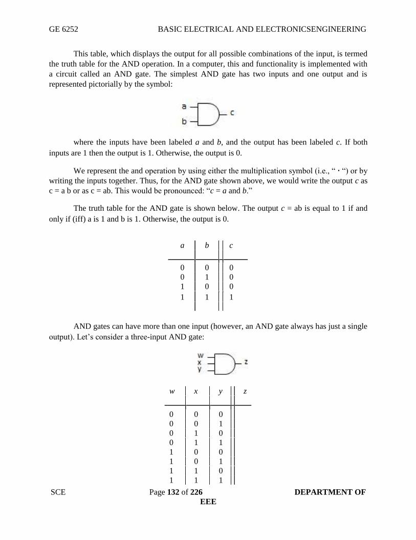
GE 6252 BASIC ELECTRICAL AND ELECTRONICSENGINEERING
SCE Page 132 of 226 DEPARTMENT OF
EEE
This table, which displays the output for all possible combinations of the input, is termed
the truth table for the AND operation. In a computer, this and functionality is implemented with
a circuit called an AND gate. The simplest AND gate has two inputs and one output and is
represented pictorially by the symbol:
where the inputs have been labeled a and b, and the output has been labeled c. If both
inputs are 1 then the output is 1. Otherwise, the output is 0.
We represent the and operation by using either the multiplication symbol (i.e., “ ∙ “) or by
writing the inputs together. Thus, for the AND gate shown above, we would write the output c as
c = a b or as c = ab. This would be pronounced: “c = a and b.”
The truth table for the AND gate is shown below. The output c = ab is equal to 1 if and
only if (iff) a is 1 and b is 1. Otherwise, the output is 0.
AND gates can have more than one input (however, an AND gate always has just a single
output). Let’s consider a three-input AND gate:
w
x
y
z
0 0 0
0 0 1
0 1 0
0 1 1
1 0 0
1 0 1
1 1 0
1 1 1
a
b
c
0 0 0
0 1 0
1 0 0
1 1 1

GE 6252 BASIC ELECTRICAL AND ELECTRONICSENGINEERING
SCE Page 133 of 226 DEPARTMENT OF
EEE
The OR Gate
Now consider the circuit shown below, that has 2 switches in parallel.
Switch S1
Switch S2
Light It is evident that the light will turn on when either switch S1 is shut or switch S2 is
shut or both are shut.
It is quite likely that you encounter the or operation in some shape or form hundreds of
times each day. Consider the simple action of sitting on your couch at home at two in the
morning studying for your Digital Logic class. Your phone will ring if you get a call from Alice
or from Bob. Your home’s security alarm will go off if the front door opens or the back door
opens. You will drink a cup of coffee if you are drowsy or you are thirsty. We can represent the light's operation using a table
S1
S2
Light
open open off
open closed on
closed open on
closed closed on
Changing the words open and off to 0 and the words shut and on to 1 and the table becomes:
S1
S2
Light
0 0 0
0 1 1
1 0 1
1 1 1
This is the truth table for the OR operation. This or functionality is implemented with a circuit
called an OR gate. The simplest OR gate has two inputs and one output and is represented
pictorially by the symbol:

GE 6252 BASIC ELECTRICAL AND ELECTRONICSENGINEERING
SCE Page 134 of 226 DEPARTMENT OF
EEE
If either or both inputs are 1, the output is 1. Otherwise, the output is 0.
We represent the or operation by using the addition symbol. Thus, for the OR gate above,
we would write the output c as c = a + b. This would be pronounced: “c = a or b.”
The truth table for the OR gate is shown below. The output is 1 if a is 1 or b is 1;
otherwise, the output is 0.
a
b
c
0 0 0
0 1 1
1 0 1
1 1 1
The NOT Gate
The last of our basic logic gates is the NOT gate. The NOT gate always has one input and
one output. If the input is 1, the output is 0. If the input is 0, the output is 1. This operation—
chaging the value of the binary input—is called complementation, negation or inversion. The
mathematical symbol for negation is an apostrophe. If the input to a NOT gate is P, the output,
termed the complement, is denoted as P’.
The pictorial symbol for a NOT gate is intended to depict an amplifier followed by a
bubble, shown below. Sometimes the NOT operation is represented by just the bubble, without
the amplifier.
The truth table for the NOT gate is shown below:
P P’
0 1
1 0
Three New Gates
Three new gates, NAND, NOR, and Exclusive-OR, can be formed from our three basic gates:
NOT, AND, and OR. NAND Gate
The logic symbol for a NAND gate is like an AND gate with a small circle (or bubble) on
the output.we see that the output of a NAND gate is 0 (low) only if both inputs are 1 (high) . The
NAND gate is equivalent to an AND gate followed by an inverter (NOT-AND).

GE 6252 BASIC ELECTRICAL AND ELECTRONICSENGINEERING
SCE Page 135 of 226 DEPARTMENT OF
EEE
NOR Gate
The logic symbol for a NOR gate is like an OR gate with a small circle (or bubble) on the
output. From the truth table .we see that the output of a NOR gate is 1 (high) only if both inputs
are 0 (low). The NOR gate is equivalent to an OR gate followed by an inverter (NOT-OR), as
shown by the two truth tables.
Exclusive-OR Gate.
The XOR gate logic symbol is like an OR gate symbol with an extra curved vertical line
on the input. From the truth table .we see that the output Z of an XOR gate is 1 (true or high) if
either input, X or Y, is 1 (true or high), but not both. The output Z will be zero if both X and Y
are the same (either both 1 or both 0). The equation for the XOR gate is given as Z = X ^ Y. In this book we will use the
symbol ^ as the XOR operator. Sometimes the symbol or the dollar sign $ is used to denote

GE 6252 BASIC ELECTRICAL AND ELECTRONICSENGINEERING
SCE Page 136 of 226 DEPARTMENT OF
EEE
Exclusive-OR. We will use the symbol ^ because that is the symbol recognized by the Verilog
software used to program a CPLD.
4.3 BOOLEAN ALGEBRA
Boolean algebra is an algebraic structure defined by a set of elements, B, together with two
binary operators, + and., provider that the following postulates are satisfied.
T1: Commutative Law (a) A+B = B+A
(b) A B = BA T2: Associative Law
(a) (A+B) +C = A+ (B+C)
(b) (A B) C = A (B C) T3: Distributive Law
(a) A (B +C) = A B + AC
(b) A + (B C) = (A +B) (A+C) T4: Identity Law
(a) A+A =A
(b) A A =A T5: Negative Law
(a) (A’) =A’
(b) (A’’) = A T6: Redundant Law
(a) A+AB=A
(b) A (A +B) =A T7: Null Law
(a) 0 + A = A
(b) 1 A = A

GE 6252 BASIC ELECTRICAL AND ELECTRONICSENGINEERING
SCE Page 137 of 226 DEPARTMENT OF
EEE
(c) 1 + A = 1
(d) 0 A = 0
T8: Double Negation Law (a) A’ +A=1
(b) A’ A=0 T9: Absorption Law
(a) A+A’B =A+B
(b) A (A’ + B) =AB T10: De Morgan's Theorem
(a) (A+B)’ = A’ B’
(b) (AB)’ = A’+B’ Example 1: Using theorems,
A + A’ B = A l + A’ B
= A (l + B) + A’B
=A + AB + A’B
=A + B (A + A’)
= A + B
Using Truth Table
A B A+B A’B A+A’B
0 0 0 0 0
0 1 1 1 1
1 0 1 0 1
1 1 1 0 1
4.3.1 Verification Of De Morgan's Theorems:
• De Morgan's First Theorem states:
The complement of a product of variables is equal to the sum of the complements of the
individual variables
• De Morgan's Second Theorem states:
The complement of sum of variables is equal to the product of the complements of

GE 6252 BASIC ELECTRICAL AND ELECTRONICSENGINEERING
SCE Page 138 of 226 DEPARTMENT OF
EEE
the dividable variables
Figure: De Morgan’s First Law Figure: De Morgan’s Second Law
4.4 ADDER 4.4.1 Half Adder
Half adder is a circuit that will add two bits & produce a sum & a carry bit. It needs two
input bits & two output bits.Fig.4.1 shows the block diagram of a half adder.
A HALF ADDER
SUM
B CARRY
Figure: Block diagram of a Half Adder
Ex-OR gate will only produce an output "1" when "EITHER" input is at logic "1", so we
need an additional output to produce a carry output, "1" when "BOTH" inputs "A" and "B" are at
logic "1" and a standard AND Gate fits the bill nicely. By combining the Ex-OR gate with the
AND gate results in a simple digital binary adder circuit known commonly as the "Half Adder"
circuit.

GE 6252 BASIC ELECTRICAL AND ELECTRONICSENGINEERING
SCE Page 139 of 226 DEPARTMENT OF
EEE
INPUTS OUTPUTS
A B SUM CARRY
0 0 0 0
0 1 1 0
1 0 1 0
1 1 0 1
Figure: Logic diagram & Truth table for half adder 4.4.2 Full Adder
A half adder has only two inputs &there is no provision to add a carry coming from the
lower order bits when multi addition is performed. For this purpose, a full adder is designed.
The 1-bit Full Adder circuit is basically two half adders connected together and consists
of three Ex-OR gates, two AND gates and an OR gate, six logic gates in total. The truth table for
the full adder includes an additional column to take into account the Carry-in input as well as the
summed output and carry-output.
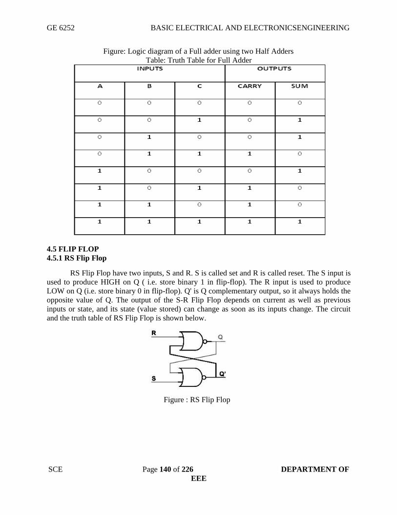
GE 6252 BASIC ELECTRICAL AND ELECTRONICSENGINEERING
SCE Page 140 of 226 DEPARTMENT OF
EEE
Figure: Logic diagram of a Full adder using two Half Adders
Table: Truth Table for Full Adder
4.5 FLIP FLOP
4.5.1 RS Flip Flop RS Flip Flop have two inputs, S and R. S is called set and R is called reset. The S input is
used to produce HIGH on Q ( i.e. store binary 1 in flip-flop). The R input is used to produce
LOW on Q (i.e. store binary 0 in flip-flop). Q' is Q complementary output, so it always holds the
opposite value of Q. The output of the S-R Flip Flop depends on current as well as previous
inputs or state, and its state (value stored) can change as soon as its inputs change. The circuit
and the truth table of RS Flip Flop is shown below.
Figure : RS Flip Flop

GE 6252 BASIC ELECTRICAL AND ELECTRONICSENGINEERING
SCE Page 141 of 226 DEPARTMENT OF
EEE
Table: Truth table for RS Flip Flop
S R Q Q+
0 0 0 0
0 0 1 1
0 1 X 0
1 0 X 1
1 1 X 0
The operation has to be analyzed with the 4 inputs combinations together with the 2 possible
previous states.
When S = 0 and R = 0: If we assume Q = 1 and Q' = 0 as initial condition, then output Q
after input is applied would be Q = (R + Q')' = 1 and Q' = (S + Q)' = 0. Assuming Q = 0
and Q' = 1 as initial condition, then output Q after the input applied would be Q = (R +
Q')' = 0 and Q' = (S + Q)' = 1. So it is clear that when both S and R inputs are LOW, the
output is retained as before the application of inputs. (i.e. there is no state change).
When S = 1 and R = 0: If we assume Q = 1 and Q' = 0 as initial condition, then output Q
after input is applied would be Q = (R + Q')' = 1 and Q' = (S + Q)' = 0. Assuming Q = 0
and Q' = 1 as initial condition, then output Q after the input applied would be Q = (R +
Q')' = 1 and Q' = (S + Q)' = 0. So in simple words when S is HIGH and R is LOW, output
Q is HIGH.
When S = 0 and R = 1: If we assume Q = 1 and Q' = 0 as initial condition, then output Q
after input is applied would be Q = (R + Q')' = 0 and Q' = (S + Q)' = 1. Assuming Q = 0
and Q' = 1 as initial condition, then output Q after the input applied would be Q = (R +
Q')' = 0 and Q' = (S + Q)' = 1. So in simple words when S is LOW and R is HIGH, output
Q is LOW.
When S = 1 and R =1 : No matter what state Q and Q' are in, application of 1 at input of
NOR gate always results in 0 at output of NOR gate, which results in both Q and Q' set to
LOW (i.e. Q = Q'). LOW in both the outputs basically is wrong, so this case is invalid.
It is possible to construct the RS Flip Flop using NAND gates (of course as seen in Logic
gates section). The only difference is that NAND is NOR gate dual form (Did I say that in Logic
gates section?). So in this case the R = 0 and S = 0 case becomes the invalid case. The circuit
and Truth table of RS Flip Flop using NAND is shown below.
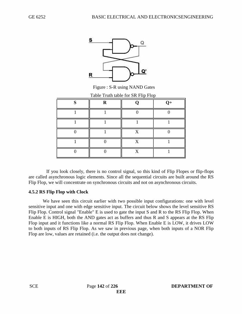
GE 6252 BASIC ELECTRICAL AND ELECTRONICSENGINEERING
SCE Page 142 of 226 DEPARTMENT OF
EEE
Figure : S-R using NAND Gates
Table Truth table for SR Flip Flop
S R Q Q+
1 1 0 0
1 1 1 1
0 1 X 0
1 0 X 1
0 0 X 1
If you look closely, there is no control signal, so this kind of Flip Flopes or flip-flops
are called asynchronous logic elements. Since all the sequential circuits are built around the RS
Flip Flop, we will concentrate on synchronous circuits and not on asynchronous circuits.
4.5.2 RS Flip Flop with Clock
We have seen this circuit earlier with two possible input configurations: one with level
sensitive input and one with edge sensitive input. The circuit below shows the level sensitive RS
Flip Flop. Control signal "Enable" E is used to gate the input S and R to the RS Flip Flop. When
Enable E is HIGH, both the AND gates act as buffers and thus R and S appears at the RS Flip
Flop input and it functions like a normal RS Flip Flop. When Enable E is LOW, it drives LOW
to both inputs of RS Flip Flop. As we saw in previous page, when both inputs of a NOR Flip
Flop are low, values are retained (i.e. the output does not change).

GE 6252 BASIC ELECTRICAL AND ELECTRONICSENGINEERING
SCE Page 143 of 226 DEPARTMENT OF
EEE
Figure : S-R with Edge Sensitive and Level sensitive Set up and Hold time
For synchronous flip-flops, we have special requirements for the inputs with respect to
clock signal input. They are
Setup Time: Minimum time period during which data must be stable before the clock
makes a valid transition. For example, for a posedge triggered flip-flop, with a setup time
of 2 ns, Input Data (i.e. R and S in the case of RS flip-flop) should be stable for at least 2
ns before clock makes transition from 0 to 1.
Hold Time: Minimum time period during which data must be stable after the clock has
made a valid transition. For example, for a posed triggered flip-flop, with a hold time of 1
ns. Input Data (i.e. R and S in the case of RS flip-flop) should be stable for at least 1 ns
after clock has made transition from 0 to 1.
If data makes transition within this setup window and before the hold window, then the
flip-flop output is not predictable, and flip-flop enters what is known as meta stable state. In this
state flip-flop output oscillates between 0 and 1. It takes some time for the flip-flop to settle
down. The whole process is called Meta stability. You could refer to tidbits section to know
more information on this topic. The waveform below shows input S (R is not shown), and CLK
and output Q (Q' is not shown) for a SR posed flip-flop.
Figure: Waveform for S-R and CLK
4.5.3 D Flip Flop
The RS Flip Flop seen earlier contains ambiguous state; to eliminate this condition we
can ensure that S and R are never equal. This is done by connecting S and R together with an
inverter. Thus we have D Flip Flop: the same as the RS Flip Flop, with the only difference that

GE 6252 BASIC ELECTRICAL AND ELECTRONICSENGINEERING
SCE Page 144 of 226 DEPARTMENT OF
EEE
there is only one input, instead of two (R and S). This input is called D or Data input. D Flip Flop
is called D transparent Flip Flop for the reasons explained earlier. Delay flip-flop or delay latch
is another name used. Below is the truth table and circuit of D Flip Flop.
In real world designs (ASIC/FPGA Designs) only D latches/Flip-Flops are used.
Figure 2.12: D Flip Flop with Edge Sensitive and Level sensitive
Table: Truth table for D Flip Flop
D Q Q+
1 X 1
0 X 0
Below is the D Flip Flop waveform, which is similar to the RS Flip Flop one, but with R
removed.
Figure: D Flip Flop waveform
4.5.5 JK Flip Flop
The ambiguous state output in the RS Flip Flop was eliminated in the D Flip Flop by
joining the inputs with an inverter. But the D Flip Flop has a single input. JK Flip Flop is similar
to RS Flip Flop in that it has 2 inputs J and K as shown Figurer below. The ambiguous state has
been eliminated here: when both inputs are high, output toggles. The only difference we see here
is output feedback to inputs, which is not there in the RS Flip Flop.

GE 6252 BASIC ELECTRICAL AND ELECTRONICSENGINEERING
SCE Page 145 of 226 DEPARTMENT OF
EEE
Figure: JK Flip Flop
Table: Truth table for JK Flip Flop
J K Q
1 1 0
1 1 1
1 0 1
0 1 0
4.4.4 T Flip Flop
When the two inputs of JK Flip Flop are shorted, a T Flip Flop is formed. It is called T
Flip Flop as, when input is held HIGH, output toggles.
Figure : T Flip Flop
Table: T Flip Flop
T Q Q+
1 0 1
1 1 0
0 1 1
0 0 0

GE 6252 BASIC ELECTRICAL AND ELECTRONICSENGINEERING
SCE Page 146 of 226 DEPARTMENT OF
EEE
4.5.6 JK Master Slave Flip-Flop
All sequential circuits that we have seen in the last few pages have a problem (All level
sensitive sequential circuits have this problem). Before the enable input changes state from
HIGH to LOW (assuming HIGH is ON and LOW is OFF state), if inputs changes, then another
state transition occurs for the same enable pulse. This sort of multiple transition problem is
called racing.
If we make the sequential element sensitive to edges, instead of levels, we can overcome
this problem, as input is evaluated only during enable/clock edges.
Figure: JK Master Slave Flip Flop
In the Figure above there are two Flip Flop, the first Flip Flop on the left is called master
Flip Flop and the one on the right is called slave Flip Flop. Master Flip Flop is positively clocked
and slave Flip Flop is negatively clocked.
Figure : JK Master Slave Flip Flop 4.7 COUNTERS
• Counters are a specific type of sequential circuit.
• Like registers, the state, or the flip-flop values themselves, serves as the “output.”
• The output value increases by one on each clock cycle.
• After the largest value, the output “wraps around” back to 0. Benefits of counters
• Counters can act as simple clocks to keep track of “time.”
GE 6252 BASIC ELECTRICAL AND ELECTRONICSENGINEERING
SCE Page 147 of 226 DEPARTMENT OF
EEE
• You may need to record how many times something has happened.
– How many bits have been sent or received?
– How many steps have been performed in some computation?
• All processors contain a program counter, or PC.
– Programs consist of a list of instructions that are to be executed one after another
(for the most part). – The PC keeps track of the instruction currently being executed.
– The PC increments once on each clock cycle, and the next program instruction is
then executed. Counter Types Asynchronous Counter (Ripple or Serial Counter)
Each FF is triggered one at a time with output of one FF serving as clock input of next FF
in the chain. Synchronous Counter (a.k.a. Parallel Counter)
All the FF‟ s in the counter are clocked at the same time. Up Counter
Counter counts from zero to a maximum count. Down Counter
Counter counts from a maximum count down to zero. BCD Counter
Counter counts from 0000 to 1001 before it recycles. Pre-settable Counter
Counter that can be preset to any starting count either synchronously or asynchronously Ring Counter
Shift register in which the output of the last FF is connected back to the input of the first
FF. Johnson Counter
Shift register in which the inverted output of the last FF is connected to the input of the
first FF.
4.7.1 Synchronous Counter
There is a problem with the ripple counter just discussed. The output stages of the flip-
flops further down the line (from the first clocked flip-flop) take time to respond to
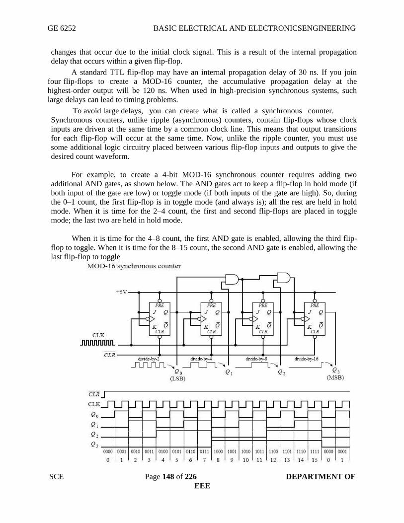
GE 6252 BASIC ELECTRICAL AND ELECTRONICSENGINEERING
SCE Page 148 of 226 DEPARTMENT OF
EEE
changes that occur due to the initial clock signal. This is a result of the internal propagation
delay that occurs within a given flip-flop. A standard TTL flip-flop may have an internal propagation delay of 30 ns. If you join
four flip-flops to create a MOD-16 counter, the accumulative propagation delay at the
highest-order output will be 120 ns. When used in high-precision synchronous systems, such
large delays can lead to timing problems. To avoid large delays, you can create what is called a synchronous counter.
Synchronous counters, unlike ripple (asynchronous) counters, contain flip-flops whose clock
inputs are driven at the same time by a common clock line. This means that output transitions
for each flip-flop will occur at the same time. Now, unlike the ripple counter, you must use
some additional logic circuitry placed between various flip-flop inputs and outputs to give the
desired count waveform.
For example, to create a 4-bit MOD-16 synchronous counter requires adding two
additional AND gates, as shown below. The AND gates act to keep a flip-flop in hold mode (if
both input of the gate are low) or toggle mode (if both inputs of the gate are high). So, during
the 0–1 count, the first flip-flop is in toggle mode (and always is); all the rest are held in hold
mode. When it is time for the 2–4 count, the first and second flip-flops are placed in toggle
mode; the last two are held in hold mode.
When it is time for the 4–8 count, the first AND gate is enabled, allowing the third flip-
flop to toggle. When it is time for the 8–15 count, the second AND gate is enabled, allowing the
last flip-flop to toggle

GE 6252 BASIC ELECTRICAL AND ELECTRONICSENGINEERING
SCE Page 149 of 226 DEPARTMENT OF
EEE
Figure: Mod 16 Synchronous Counters and Cycle Diagram
The ripple (asynchronous) and synchronous counters discussed so far are simple but
hardly ever used. In practice, if you need a counter, be it ripple or synchronous, you go out and
purchase a counter IC. These ICs are often MOD-16 or MOD-10 counters and usually come with
many additional features. For example, many ICs allow you to preset the count to a desired
number via parallel input lines.
Synchronous Up /Down Counter
The down counter counts in reverse from 1111 to 0000 and then goes to 1111. If we
inspect the count cycle, we find that each flip-flop will complement when the previous flip- flops
are all 0 (this is the opposite of the up counter). The down counter can be implemented similar to
the up counter, except that the AND gate input is taken from Q’ instead of Q. This is shown in
the following Figure of a 4-bit up-down counter using T flip-flops.
Figure: Synchronous Up /Down Counter
4.7.2 Asynchronous Up /Down Counter:
In certain applications, a counter must be able to count both up and down. The circuit
below is a 3-bit up-down counter. It counts up or down depending on the status of the control
signals UP and DOWN. When the UP input is at 1 and the DOWN input is at 0, the NAND
network between FF0 and FF1 will gate the non-inverted output (Q) of FF0 into the clock input
of FF1. Similarly, Q of FF1 will be gated through the other NAND network into the clock
input of FF2. Thus the counter will count up.

GE 6252 BASIC ELECTRICAL AND ELECTRONICSENGINEERING
SCE Page 150 of 226 DEPARTMENT OF
EEE
Figure: Asynchronous Up /Down Counter When the control input UP is at 0 and DOWN is at 1, the inverted outputs of FF0 and
FF1 are gated into the clock inputs of FF1 and FF2 respectively. If the flip-flops are initially y
reset to 0's, then the counter will go through the following sequence as input pulses are applied
Notice that an asynchronous up-down counter is slower than an up counter or a down
counter because of the additional propagation delay introduced by the NAND networks.
Design of Synchronous Counters
This section begins our study of designing an important class of clocked sequential logic
circuits-synchronous fi ni t e -state machines. Like all sequential circuits, a finite-state machine
determines its outputs and its next state from its current inputs and current state. A synchronous
finite state machine changes state only on the clocking event. 4.8 ANALOG TO DIGITAL CONVERSION
A comparator compares the unknown voltage with a known value of voltage and then
produces proportional output (i.e. it will produce either a 1 or a 0). This principle is basically
used in the above circuit. Here three comparators are used. Each has two inputs. One input of
each comparator is connected to analog input voltage. The other input terminals are connected to
fixed reference voltage like +3/4V, +V/2 and +V/4. Now the circuit can convert analog voltage
into equivalent digital signal. Since the analog output voltage is connected in parallel to all the
comparators, the circuit is also called as parallel A/D converter.
Figure: ADC Conversion

GE 6252 BASIC ELECTRICAL AND ELECTRONICSENGINEERING
SCE Page 151 of 226 DEPARTMENT OF
EEE
Working – Here each comparator is connected to a reference voltage of +3/4V, +V/2 and
+V/4 with their outputs as C3C2C1 respectively. Now suppose the analog input voltage change
from 0 – 4V, then the actual values of reference voltages will be +3/4V = 3V, +V/2 =2V and
+V/4 =1V. Now there will be following conditions of outputs of the circuit
1) When input voltage is between 0 and 1V, the output will be C3C2C1 = 000.
2) When input voltage > 1V £ 2V, the output will be C3C2C1 = 001.
3) When input voltage > 2V £ 3V, the output will be C3C2C1 = 011.
4) When input voltage > 3V £ 4V, the output will be C3C2C1 = 111.
In this way, the circuit can convert the analog input voltage into its equivalent or
proportional binary number in digital style. 4.8.1 Successive Approximation Technique
The basic drawback of counter method (given above) is that it has longer conversion
time. Because it always starts from 0000 at every measurement, until the analog voltage is
matched. This drawback is removed in successive approximation method. In the adjacent figure,
the method of successive approximation technique is shown. When unknown voltage (Va) is
applied, the circuit starts up from 0000, as shown above. The output of SAR advances with each
MSB. The output of SAR does not increase step–by–step in BCD bus pattern, but individual bit
becomes high–starting from MSB. Then by comparison, the bit is fixed or removed. Thus, it sets
first MSB (1000), then the second MSB (0100) and so on. Every time, the output of SAR is
converted to equivalent analog voltage by binary ladder. It is then compared with applied
unknown voltage (Va). The comparison process goes on, in binary search style, until the binary
equivalent of analog voltage is obtained. In this way following steps are carried out during
conversion.
Figure: Successive Approximation Technique Now refer the following figure and the given steps -
1) The unknown analog voltage (Va) is applied.

GE 6252 BASIC ELECTRICAL AND ELECTRONICSENGINEERING
SCE Page 152 of 226 DEPARTMENT OF
EEE
2) Starts up from 0000 and sets up first MSB 1000.
3) If Va >= 1000, the first MSB is fixed.
4) If Va < 1000, the first MSB is removed and second MSB is set
5) The fixing and removing the MSBs continues up to last bit (LSB), until equivalent binary
output is obtained.
Figure 3.38 Equivalent Binary Output 4.8.2 Flash ADC Also called the parallel A/D converter, this circuit is the simplest to understand. It is
formed of a series of comparators, each one comparing the input signal to a unique reference
voltage. The comparator outputs connect to the inputs of a priority encoder circuit, which then
produces a binary output.
Figure: Flash ADC

GE 6252 BASIC ELECTRICAL AND ELECTRONICSENGINEERING
SCE Page 153 of 226 DEPARTMENT OF
EEE
The following illustration shows a 3-bit flash ADC circuit:
Vref is a stable reference voltage provided by a precision voltage regulator as part of the
converter circuit, not shown in the schematic. As the analog input voltage exceeds the reference
voltage at each comparator, the comparator outputs will sequentially saturate to a high state. The
priority encoder generates a binary number based on the highest-order active input, ignoring all
other active inputs. When operated, the flash ADC produces an output that looks something like this
igure: Outputs
4.8 DIGITAL TO ANALOG CONVERTER (DAC):
The process of converting digital signal into equivalent analog signal is called D/A
conversion. The electronics circuit, which does this process, is called D/A converter. The circuit
has „n’ number of digital data inputs with only one output. Basically, there are two types of D/A
converter circuits: Weighted resistors D/A converter circuit and Binary ladder or R–2R ladder
D/A converter circuit.
4.8.1 Weighted resistors D/A converter
Here an OPAMP is used as summing amplifier. There are four resistors R, 2R, 4R and
8R at the input terminals of the OPAMP with R as feedback resistor. The network of resistors at
the input terminal of OPAMP is called as variable resistor network. The four inputs of the circuit
are D, C, B & A. Input D is at MSB and A is at LSB. Here we shall connect 8V DC voltage as
logic–1 level. So we shall assume that 0 = 0V and 1 = 8V.
Figure: Weighted resistors D/A converter
GE 6252 BASIC ELECTRICAL AND ELECTRONICSENGINEERING
SCE Page 154 of 226 DEPARTMENT OF
EEE
Now the working of the circuit is as follows. Since the circuit is summing amplifier, its
output is given by the following equation –
Working of the circuit
When input DCBA = 0000, then putting these value in above equation (1) we get –
When digital input of the circuit DCBA = 0001, then putting these value in above
equation (1) we get
When digital input of the circuit DCBA = 0010, then putting these value in above
equation (1) we get – …………… so on.
In this way, when digital input changes from 0000 to 1111 (in BCD style), output voltage
(Vo) changes proportionally. This is given in the conversion chart. There are some main
disadvantages of the circuit.
They are
1) Each resistor in the circuit has different value.
2) So error in value of each resistor adds up.
3) The value of resistor at MSB is the lowest. Hence, it draws more current.
4) Also, its heat & power dissipation is very high.
5) There is the problem of impedance matching due to different values of resistors. 4.8.2 R–2R Ladder D/A Converter
It is modern type of resistor network. It has only two values of resistors the R and 2R.
These values repeat throughout in the circuit. The OPAMP is used at output for scaling the
output voltage. The working of the circuit can be understood as follows. For simplicity, we
ignore the OPAMP in the above circuit (this is because its gain is unity). Now consider the
circuit, without OPAMP. Suppose the digital input is DCBA = 1000. Then the circuit is reduced
to a small circuit.

GE 6252 BASIC ELECTRICAL AND ELECTRONICSENGINEERING
SCE Page 155 of 226 DEPARTMENT OF
EEE
Its output is given by –
Reduced circuit of R-2R ladder, when we consider that all inputs=0
Now suppose digital input of the same circuit is changed to DCBA = 0100. Then the
output voltage will be V/4, when DCBA = 0010, output voltage will be V/8, for DCBA = 0001,
output voltage will be V/16 and so on. The general formula for the above circuit of R–2R ladder,
including the OPAMP also, will be – You can take (R) common from the above formula and simplify it. With the help of this
formula, we can calculate any combination of digital input into its equivalent analog voltage at
the output terminals.

GE 6252 BASIC ELECTRICAL AND ELECTRONICSENGINEERING
SCE Page 156 of 226 DEPARTMENT OF
EEE
UNIT – V FOUNDAMENTALS OF COMMUNICATION ENGINNERING
5.1. Types of signal
Analog signal and digital signal
Definitions of Analog vs Digital signals
An Analog signal is any continuous signal for which the time varying feature (variable) of the
signal is a representation of some other time varying quantity, i.e., analogous to another time
varying signal. It differs from a digital signal in terms of small fluctuations in the signal which
are meaningful.
A digital signal uses discrete (discontinuous) values. By contrast, non-digital (or analog)
systems use a continuous range of values to represent information. Although digital
representations are discrete, the information represented can be either discrete, such as numbers
or letters, or continuous, such as sounds, images, and other measurements of continuous systems.
Properties of Digital vs Analog signals
Digital information has certain properties that distinguish it from analog communication
methods. These include
Synchronization – digital communication uses specific synchronization sequences for
determining synchronization.
Language – digital communications requires a language which should be possessed by both
sender and receiver and should specify meaning of symbol sequences.
Errors – disturbances in analog communication causes errors in actual intended communication
but disturbances in digital communication does not cause errors enabling error free
communication. Errors should be able to substitute, insert or delete symbols to be expressed.
Copying – analog communication copies are quality wise not as good as their originals while
due to error free digital communication, copies can be made indefinitely.
Granularity – for a continuously variable analog value to be represented in digital form there
occur quantization error which is difference in actual analog value and digital representation and
this property of digital communication is known as granularity.
Differences in Usage in Equipment
Many devices come with built in translation facilities from analog to digital. Microphones and
speaker are perfect examples of analog devices. Analog technology is cheaper but there is a
limitation of size of data that can be transmitted at a given time.
Digital technology has revolutionized the way most of the equipments work. Data is converted
into binary code and then reassembled back into original form at reception point. Since these can
be easily manipulated, it offers a wider range of options. Digital equipment is more expensive
than analog equipment.

GE 6252 BASIC ELECTRICAL AND ELECTRONICSENGINEERING
SCE Page 157 of 226 DEPARTMENT OF
EEE
Comparison of Analog vs Digital Quality
Digital devices translate and reassemble data and in the process are more prone to loss of quality
as compared to analog devices. Computer advancement has enabled use of error detection and
error correction techniques to remove disturbances artificially from digital signals and improve
quality.
Differences in Applications
Digital technology has been most efficient in cellular phone industry. Analog phones have
become redundant even though sound clarity and quality was good.
Analog technology comprises of natural signals like human speech. With digital technology this
human speech can be saved and stored in a computer. Thus digital technology opens up the
horizon for endless possible uses.
Comparison chart
Analog Digital
Signal
Analog signal is a continuous signal
which represents physical
measurements.
Digital signals are discrete time signals
generated by digital modulation.
Waves Denoted by sine waves Denoted by square waves
Representation Uses continuous range of values to
represent information
Uses discrete or discontinuous values to
represent information
Example Human voice in air, analog
electronic devices.
Computers, CDs, DVDs, and other digital
electronic devices.
Technology Analog technology records
waveforms as they are.
Samples analog waveforms into a limited
set of numbers and records them.
Data
transmissions
Subjected to deterioration by noise
during transmission and write/read
cycle.
Can be noise-immune without deterioration
during transmission and write/read cycle.
Response to
Noise
More likely to get affected reducing
accuracy
Less affected since noise response are
analog in nature
Flexibility Analog hardware is not flexible. Digital hardware is flexible in
implementation.
Uses
Can be used in analog devices only.
Best suited for audio and video
transmission.
Best suited for Computing and digital
electronics.
Applications Thermometer PCs, PDAs

GE 6252 BASIC ELECTRICAL AND ELECTRONICSENGINEERING
SCE Page 158 of 226 DEPARTMENT OF
EEE
Analog Digital
Bandwidth
Analog signal processing can be
done in real time and consumes less
bandwidth.
There is no guarantee that digital signal
processing can be done in real time and
consumes more bandwidth to carry out the
same information.
Memory Stored in the form of wave signal Stored in the form of binary bit
Power Analog instrument draws large
power
Digital instrument drawS only negligible
power
Cost Low cost and portable Cost is high and not easily portable
Impedance Low High order of 100 megaohm
Errors
Analog instruments usually have a
scale which is cramped at lower end
and give considerable observational
errors.
Digital instruments are free from
observational errors like parallax and
approximation errors.
5.2. Principles of Amplitude modulation
Amplitude Modulation (AM) plus frequency division multiplexing (FDM) is one
way of solving above problem. Each conversation is shifted to a different part of
the frequency spectrum by using a high-frequency waveform to "carry" each
individual speech signal. These high frequencies are called carrier frequencies .
Amplitude modulation is the process of varying the amplitude of the sinusoidal
carrier wave by the amplitude of the modulating signal, and is illustrated in Fig.
The unmodulated carrier wave has a constant peak value and a higher
frequency than the modulating signal , but, when the modulating signal is applied,
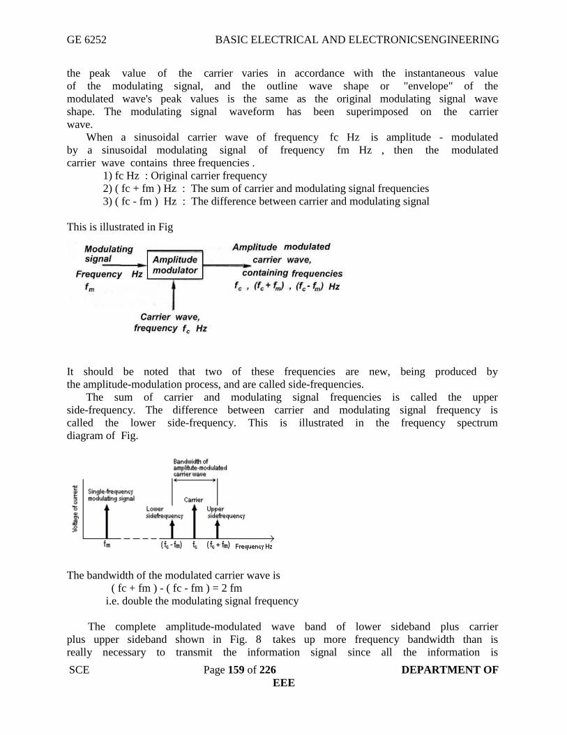
GE 6252 BASIC ELECTRICAL AND ELECTRONICSENGINEERING
SCE Page 159 of 226 DEPARTMENT OF
EEE
the peak value of the carrier varies in accordance with the instantaneous value
of the modulating signal, and the outline wave shape or "envelope" of the
modulated wave's peak values is the same as the original modulating signal wave
shape. The modulating signal waveform has been superimposed on the carrier
wave.
When a sinusoidal carrier wave of frequency fc Hz is amplitude - modulated
by a sinusoidal modulating signal of frequency fm Hz , then the modulated
carrier wave contains three frequencies .
1) fc Hz : Original carrier frequency
2) ( fc + fm ) Hz : The sum of carrier and modulating signal frequencies
3) ( fc - fm ) Hz : The difference between carrier and modulating signal
This is illustrated in Fig
It should be noted that two of these frequencies are new, being produced by
the amplitude-modulation process, and are called side-frequencies.
The sum of carrier and modulating signal frequencies is called the upper
side-frequency. The difference between carrier and modulating signal frequency is
called the lower side-frequency. This is illustrated in the frequency spectrum
diagram of Fig.
The bandwidth of the modulated carrier wave is
( fc + fm ) - ( fc - fm ) = 2 fm
i.e. double the modulating signal frequency
The complete amplitude-modulated wave band of lower sideband plus carrier
plus upper sideband shown in Fig. 8 takes up more frequency bandwidth than is
really necessary to transmit the information signal since all the information is

GE 6252 BASIC ELECTRICAL AND ELECTRONICSENGINEERING
SCE Page 160 of 226 DEPARTMENT OF
EEE
carried by either one of the sidebands alone . The carrier component is of constant
amplitude and frequency so does not carry any of the information signal at all . It is
possible by using special equipment to suppress both the carrier and one sideband
and to transmit just the other sideband with no loss of information. This method of
working is called single sideband working ( SSB ) . This method is not used for
domestic radio broadcasting , but it is used for some long-distance radio telephony
systems and for multi-channel carrier systems used in national telephone networks.
5.3 Principle of frequency modulation
Frequency modulation uses the information signal, Vm(t) to vary the carrier frequency within
some small range about its original value. Here are the three signals in mathematical form:
Information: Vm(t)
Carrier: Vc(t) = Vco sin ( 2 p fc t + f )
FM: VFM (t) = Vco sin (2 p [fc + (Df/Vmo) Vm (t) ] t + f)
We have replaced the carrier frequency term, with a time-varying frequency. We have also
introduced a new term: Df, the peak frequency deviation. In this form, you should be able to see
that the carrier frequency term: fc + (Df/Vmo) Vm (t) now varies between the extremes of fc - Df
and fc + Df. The interpretation of Df becomes clear: it is the farthest away from the original
frequency that the FM signal can be. Sometimes it is referred to as the "swing" in the frequency.
We can also define a modulation index for FM, analogous to AM:
b = Df/fm , where fm is the maximum modulating frequency used.
The simplest interpretation of the modulation index, b, is as a measure of the peak frequency
deviation, Df. In other words, b represents a way to express the peak deviation frequency as a
multiple of the maximum modulating frequency, fm, i.e. Df = b fm.
Example: suppose in FM radio that the audio signal to be transmitted ranges from 20 to 15,000
Hz (it does). If the FM system used a maximum modulating index, b, of 5.0, then the frequency
would "swing" by a maximum of 5 x 15 kHz = 75 kHz above and below the carrier frequency.
Here is a simple FM signal:
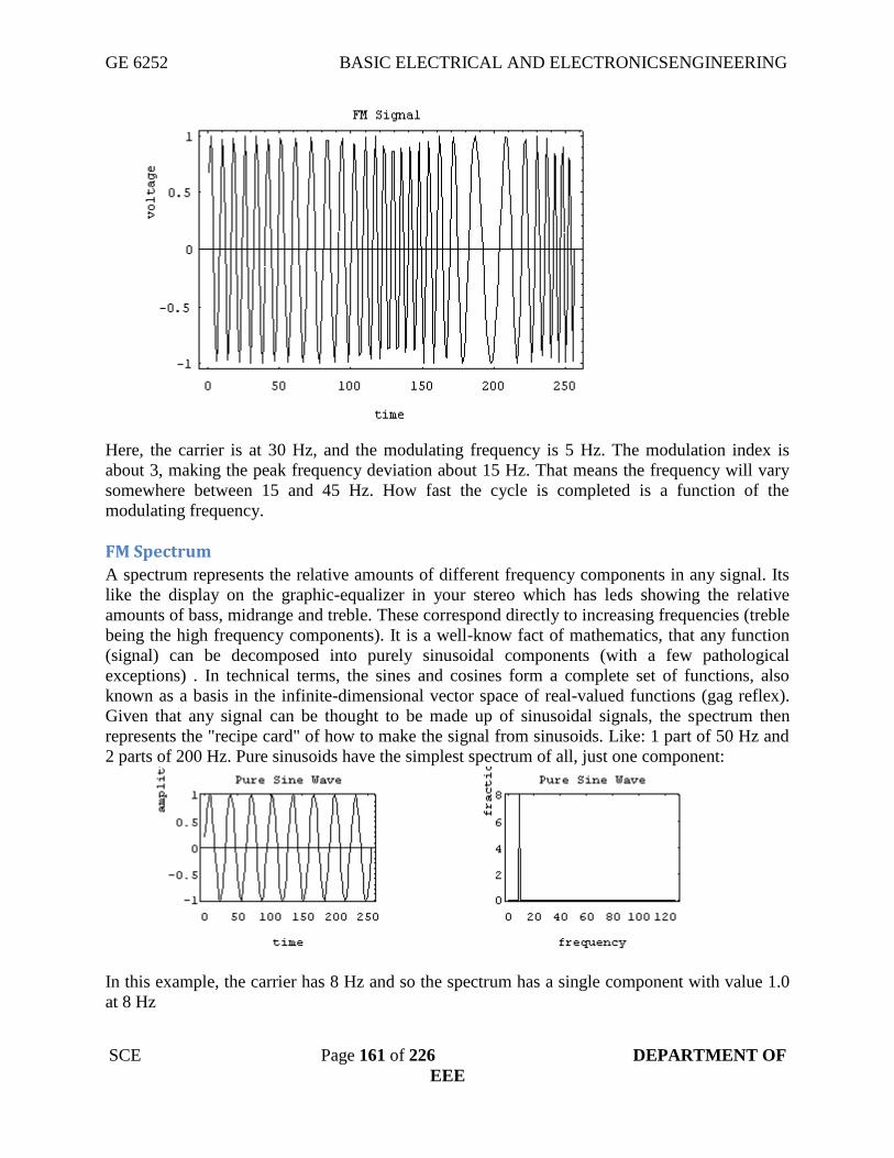
GE 6252 BASIC ELECTRICAL AND ELECTRONICSENGINEERING
SCE Page 161 of 226 DEPARTMENT OF
EEE
Here, the carrier is at 30 Hz, and the modulating frequency is 5 Hz. The modulation index is
about 3, making the peak frequency deviation about 15 Hz. That means the frequency will vary
somewhere between 15 and 45 Hz. How fast the cycle is completed is a function of the
modulating frequency.
FM Spectrum
A spectrum represents the relative amounts of different frequency components in any signal. Its
like the display on the graphic-equalizer in your stereo which has leds showing the relative
amounts of bass, midrange and treble. These correspond directly to increasing frequencies (treble
being the high frequency components). It is a well-know fact of mathematics, that any function
(signal) can be decomposed into purely sinusoidal components (with a few pathological
exceptions) . In technical terms, the sines and cosines form a complete set of functions, also
known as a basis in the infinite-dimensional vector space of real-valued functions (gag reflex).
Given that any signal can be thought to be made up of sinusoidal signals, the spectrum then
represents the "recipe card" of how to make the signal from sinusoids. Like: 1 part of 50 Hz and
2 parts of 200 Hz. Pure sinusoids have the simplest spectrum of all, just one component:
In this example, the carrier has 8 Hz and so the spectrum has a single component with value 1.0
at 8 Hz
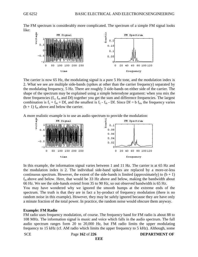
GE 6252 BASIC ELECTRICAL AND ELECTRONICSENGINEERING
SCE Page 162 of 226 DEPARTMENT OF
EEE
The FM spectrum is considerably more complicated. The spectrum of a simple FM signal looks
like:
The carrier is now 65 Hz, the modulating signal is a pure 5 Hz tone, and the modulation index is
2. What we see are multiple side-bands (spikes at other than the carrier frequency) separated by
the modulating frequency, 5 Hz. There are roughly 3 side-bands on either side of the carrier. The
shape of the spectrum may be explained using a simple heterodyne argument: when you mix the
three frequencies (fc, fm and Df) together you get the sum and difference frequencies. The largest
combination is fc + fm + Df, and the smallest is fc - fm - Df. Since Df = b fm, the frequency varies
(b + 1) fm above and below the carrier.
A more realistic example is to use an audio spectrum to provide the modulation:
In this example, the information signal varies between 1 and 11 Hz. The carrier is at 65 Hz and
the modulation index is 2. The individual side-band spikes are replaced by a more-or-less
continuous spectrum. However, the extent of the side-bands is limited (approximately) to (b + 1)
fm above and below. Here, that would be 33 Hz above and below, making the bandwidth about
66 Hz. We see the side-bands extend from 35 to 90 Hz, so out observed bandwidth is 65 Hz.
You may have wondered why we ignored the smooth humps at the extreme ends of the
spectrum. The truth is that they are in fact a by-product of frequency modulation (there is no
random noise in this example). However, they may be safely ignored because they are have only
a minute fraction of the total power. In practice, the random noise would obscure them anyway.
Example: FM Radio
FM radio uses frequency modulation, of course. The frequency band for FM radio is about 88 to
108 MHz. The information signal is music and voice which falls in the audio spectrum. The full
audio spectrum ranges form 20 to 20,000 Hz, but FM radio limits the upper modulating
frequency to 15 kHz (cf. AM radio which limits the upper frequency to 5 kHz). Although, some

GE 6252 BASIC ELECTRICAL AND ELECTRONICSENGINEERING
SCE Page 163 of 226 DEPARTMENT OF
EEE
of the signal may be lost above 15 kHz, most people can't hear it anyway, so there is little loss of
fidelity. FM radio maybe appropriately referred to as "high-fidelity."
If FM transmitters use a maximum modulation index of about 5.0, so the resulting bandwidth is
180 kHz (roughly 0.2 MHz). The FCC assigns stations ) 0.2 MHz apart to prevent overlapping
signals (coincidence? I think not!). If you were to fill up the FM band with stations, you could
get 108 - 88 / .2 = 100 stations, about the same number as AM radio (107). This sounds
convincing, but is actually more complicated (agh!).
FM radio is broadcast in stereo, meaning two channels of information. In practice, they generate
three signals prior to applying the modulation:
the L + R (left + right) signal in the range of 50 to 15,000 Hz.
a 19 kHz pilot carrier.
the L-R signal centered on a 38 kHz pilot carrier (which is suppressed) that ranges from 23 to 53
kHz .
So, the information signal actually has a maximum modulating frequency of 53 kHz, requiring a
reduction in the modulation index to about 1.0 to keep the total signal bandwidth about 200 kHz.
FM Performance
Bandwidth
As we have already shown, the bandwidth of a FM signal may be predicted using:
BW = 2 (b + 1 ) fm
where b is the modulation index and
fm is the maximum modulating frequency used.
FM radio has a significantly larger bandwidth than AM radio, but the FM radio band is also
larger. The combination keeps the number of available channels about the same.
The bandwidth of an FM signal has a more complicated dependency than in the AM case (recall,
the bandwidth of AM signals depend only on the maximum modulation frequency). In FM, both
the modulation index and the modulating frequency affect the bandwidth. As the information is
made stronger, the bandwidth also grows.
Efficiency
The efficiency of a signal is the power in the side-bands as a fraction of the total. In FM signals,
because of the considerable side-bands produced, the efficiency is generally high. Recall that
conventional AM is limited to about 33 % efficiency to prevent distortion in the receiver when
the modulation index was greater than 1. FM has no analogous problem.
The side-band structure is fairly complicated, but it is safe to say that the efficiency is generally
improved by making the modulation index larger (as it should be). But if you make the
modulation index larger, so make the bandwidth larger (unlike AM) which has its disadvantages.
As is typical in engineering, a compromise between efficiency and performance is struck. The
modulation index is normally limited to a value between 1 and 5, depending on the application.

GE 6252 BASIC ELECTRICAL AND ELECTRONICSENGINEERING
SCE Page 164 of 226 DEPARTMENT OF
EEE
Noise
FM systems are far better at rejecting noise than AM systems. Noise generally is spread
uniformly across the spectrum (the so-called white noise, meaning wide spectrum). The
amplitude of the noise varies randomly at these frequencies. The change in amplitude can
actually modulate the signal and be picked up in the AM system. As a result, AM systems are
very sensitive to random noise. An example might be ignition system noise in your car. Special
filters need to be installed to keep the interference out of your car radio.
FM systems are inherently immune to random noise. In order for the noise to interfere, it would
have to modulate the frequency somehow. But the noise is distributed uniformly in frequency
and varies mostly in amplitude. As a result, there is virtually no interference picked up in the FM
receiver. FM is sometimes called "static free, " referring to its superior immunity to random
noise.
5.4.Block diagram of radio
AM Transmitter
In order to better understand the way the radio transmitter works, block - diagram of a simple
AM (amplitude modulated) signal transmitter is shown on Pic. The amplitude modulation is
being performed in a stage called the modulator. Two signals are entering it: high frequency
signal called the carrier (or the signal carrier), being created into the HF oscillator and amplified
in the HF amplifier to the required signal level, and the low frequency (modulating) signal
coming from the microphone or some other LF signal source (cassette player, record player, CD
player etc.), being amplified in the LF amplifier. On modulator's output the amplitude modulated
signal UAM is acquired. This signal is then amplified in the power amplifier, and then led to the
emission antenna.

GE 6252 BASIC ELECTRICAL AND ELECTRONICSENGINEERING
SCE Page 165 of 226 DEPARTMENT OF
EEE
The shape and characteristics of the AM carrier, being taken from the HF amplifier into the
modulator, are shown on Pic. As you can see, it is a HF voltage of constant amplitude US and
frequency fS. On Pic. the LF signal that appears at the input of the modulator at the moment t0 is
shown. With this signal the modulation of the carrier's amplitude is being performed, therefore it
is being called the modulating signal. The shape of the AM signal exiting the modulator is shown
on Pic. From the point t0 this voltage has the same shape as that on Pic. From the moment t0 the
amplitude of AM signal is being changed in accordance with the current value of the modulating
signal, in such a way that the signal envelope (fictive line connecting the voltage peaks) has the
same shape as the modulating signal.
Let's take a look at a practical example. Let the LF signal on Pic. be, say, an electrical image of
the tone being created by some musical instrument, and that the time gap between the points t0
and t2 is 1 ms. Suppose that carrier frequency is fS=1 MHz (approximately the frequency of
radio Kladovo, exact value is 999 kHz). In that case, in period from t0 till t2 signals us on Pic.
and AM on should make a thousand oscillations and not just eighteen, as shown in the picture.
Then It is clear that it isn't possible to draw a realistic picture, since all the lines would connect
into a dark spot. The true picture of AM signal from this example is given on Pic. That is the
picture that appears on screen of the oscilloscope, connected on the output of the modulator: light
coloured lines representing the AM signal have interconnected, since they are thicker than the
gap between them.
Block - diagram on Pic is a simplified schematic of an AM transmitter. In reality there are some
additional stages in professional transmitters that provide the necessary work stability,
transmitter power supply, cooling for certain stages etc. For simple use, however, even simpler
block diagrams exist, making the completion of an ordinary AM transmitter possible with just a
few electronic components.

GE 6252 BASIC ELECTRICAL AND ELECTRONICSENGINEERING
SCE Page 166 of 226 DEPARTMENT OF
EEE
FM Transmitter
Block diagram of an FM (frequency modulated) transmitter is given on Pic.2.4. Information
being transferred, i.e. the modulating signal, is a signal from some LF source. it is being
amplified in LF amplifier and then led into the HF oscillator, where the carrier signal is being
created. The carrier is a HF voltage of constant amplitude, whose frequency is, in the absence of
modulating signal, equal to the transmitter's carrier frequency fS. In the oscillatory circuit of the
HF oscillator a varicap (capacitive) diode is located. It is a diode whose capacitance depends
upon the voltage between its ends, so when being exposed to LF voltage, its capacitance is
changing in accordance with this voltage. Due to that frequency of the oscillator is also
changing, i.e. the frequency modulation is being obtained. The FM signal from the HF oscillator
is being proceeded to the power amplifier that provides the necessary output power of the
transmission signal.
Voltage shapes in FM transmitter are given on Pic.2.5. Pic.2.5-a shows the LF modulating signal.
The frequency modulation begins at moment t0 and the transmission frequency begins to change,
as shown on Pic.2.5-b: Whilst current value of the LF signal is raising so is the trasmitter
frequency, and when it is falling the frequency is also falling. As seen on Pic.2.5-c, the
information (LF signal) is being implied in frequency change of the carrier.
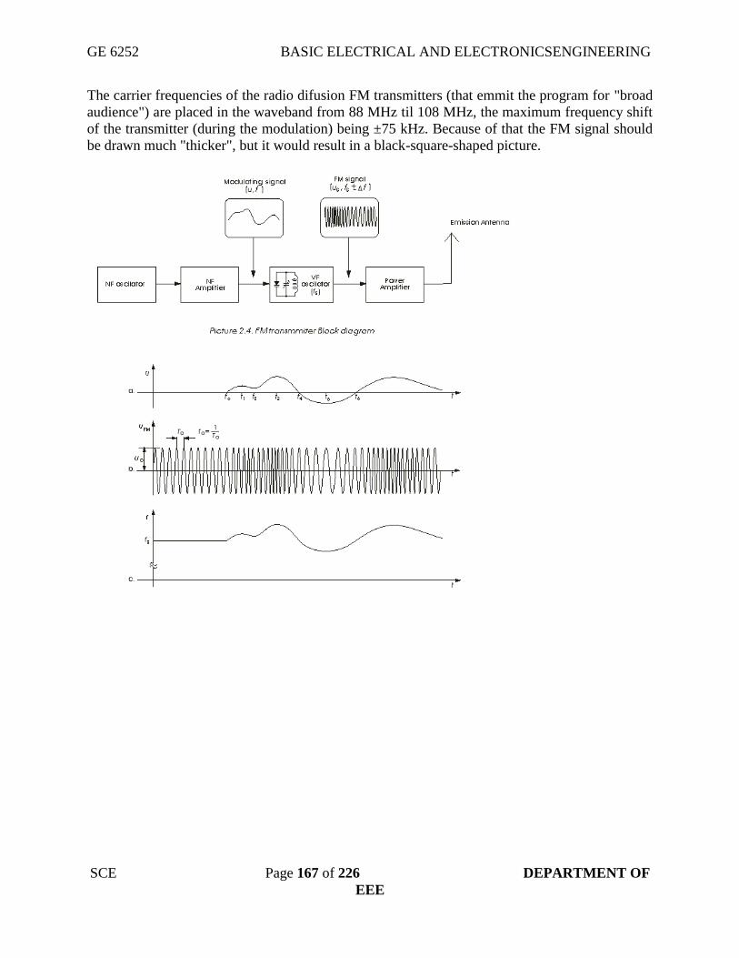
GE 6252 BASIC ELECTRICAL AND ELECTRONICSENGINEERING
SCE Page 167 of 226 DEPARTMENT OF
EEE
The carrier frequencies of the radio difusion FM transmitters (that emmit the program for "broad
audience") are placed in the waveband from 88 MHz til 108 MHz, the maximum frequency shift
of the transmitter (during the modulation) being ±75 kHz. Because of that the FM signal should
be drawn much "thicker", but it would result in a black-square-shaped picture.
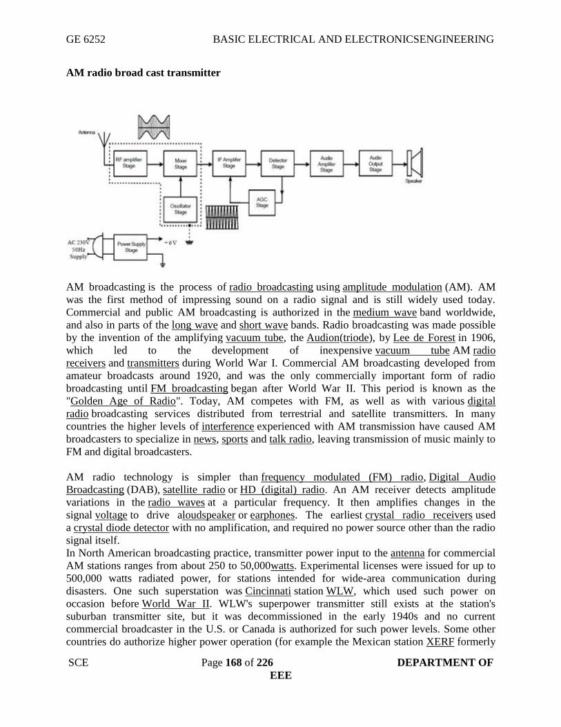
GE 6252 BASIC ELECTRICAL AND ELECTRONICSENGINEERING
SCE Page 168 of 226 DEPARTMENT OF
EEE
AM radio broad cast transmitter
AM broadcasting is the process of radio broadcasting using amplitude modulation (AM). AM
was the first method of impressing sound on a radio signal and is still widely used today.
Commercial and public AM broadcasting is authorized in the medium wave band worldwide,
and also in parts of the long wave and short wave bands. Radio broadcasting was made possible
by the invention of the amplifying vacuum tube, the Audion(triode), by Lee de Forest in 1906,
which led to the development of inexpensive vacuum tube AM radio
receivers and transmitters during World War I. Commercial AM broadcasting developed from
amateur broadcasts around 1920, and was the only commercially important form of radio
broadcasting until FM broadcasting began after World War II. This period is known as the
"Golden Age of Radio". Today, AM competes with FM, as well as with various digital
radio broadcasting services distributed from terrestrial and satellite transmitters. In many
countries the higher levels of interference experienced with AM transmission have caused AM
broadcasters to specialize in news, sports and talk radio, leaving transmission of music mainly to
FM and digital broadcasters.
AM radio technology is simpler than frequency modulated (FM) radio, Digital Audio
Broadcasting (DAB), satellite radio or HD (digital) radio. An AM receiver detects amplitude
variations in the radio waves at a particular frequency. It then amplifies changes in the
signal voltage to drive aloudspeaker or earphones. The earliest crystal radio receivers used
a crystal diode detector with no amplification, and required no power source other than the radio
signal itself.
In North American broadcasting practice, transmitter power input to the antenna for commercial
AM stations ranges from about 250 to 50,000watts. Experimental licenses were issued for up to
500,000 watts radiated power, for stations intended for wide-area communication during
disasters. One such superstation was Cincinnati station WLW, which used such power on
occasion before World War II. WLW's superpower transmitter still exists at the station's
suburban transmitter site, but it was decommissioned in the early 1940s and no current
commercial broadcaster in the U.S. or Canada is authorized for such power levels. Some other
countries do authorize higher power operation (for example the Mexican station XERF formerly

GE 6252 BASIC ELECTRICAL AND ELECTRONICSENGINEERING
SCE Page 169 of 226 DEPARTMENT OF
EEE
operated at 250,000 watts). Antenna design must consider the coverage desired and stations may
be required, based on the terms of their license, to directionalize their transmitted signal to avoid
interfering with other stations operating on the same frequency.
Radio receiver
In the early days of what is now known as early radio transmissions, say about 100 years ago,
signals were generated by various means but only up to the L.F. region.
Communication was by way of morse code much in the form that a short transmission denoted a
dot (dit) and a longer transmission was a dash (dah). This was the only form of radio
transmission until the 1920's and only of use to the military, commercial telegraph companies
and amateur experimenters.
Then it was discovered that if the amplitude (voltage levels - plus and minus about zero) could
be controlled or varied by a much lower frequency such as A.F. then real intelligence could be
conveyed e.g. speech and music. This process could be easily reversed by simple means at the
receiving end by using diode detectors. This is called modulation and obviously in this case
amplitude modulation or A.M.
This discovery spawned whole new industries and revolutionized the world of communications.
Industries grew up manufacturing radio parts, receiver manufacturers, radio stations, news
agencies, recording industries etc.
Disadvantages to A.M. radio
Firstly because of the modulation process we generate at least two copies of the intelligence plus
the carrier. For example consider a local radio station transmitting on say 900 Khz. This
frequency will be very stable and held to a tight tolerance. To suit our discussion and keep it as
simple as possible we will have the transmission modulated by a 1000 Hz or 1Khz tone.
At the receiving end 3 frequencies will be available. 900 Khz, 901 Khz and 899 Khz i.e. the
original 900 Khz (the carrier) plus and minus the modulating frequency which are called side
bands. For very simple receivers such as a cheap transistor radio we only require the original
plus either one of the side bands. The other one is a total waste. For sophisticated receivers one
side band can be eliminated.
The net effect is A.M. radio stations are spaced 10 Khz apart (9 kHz in Australia) e.g. 530
Khz...540 Khz...550 Khz. This spacing could be reduced and nearly twice as many stations
accommodated by deleting one side band. Unfortunately the increased cost of receiver
complexity forbids this but it certainly is feasible

GE 6252 BASIC ELECTRICAL AND ELECTRONICSENGINEERING
SCE Page 170 of 226 DEPARTMENT OF
EEE
Block diagram of television transmitter
The basic television Broadcast transmitter block diagram is shown in figure (a).
The block diagram can be broadly divided into two separate section, viz., one that - Generates an
electronic signal (called video signal) corresponding to the actual picture and then uses this video
signal to modulate an R-F carrier so as to be applied to the transmitting antenna for transmission,
other that generates an electronic signal (called audio signal) containing sound information and
then uses this signal to modulate another RF carrier and then applied to the transmitting antenna
for transmission.
However only one antenna is used for transmission of the video as well as audio signals. Thus
these modulated signals have to be combined together in some appropriate network. In addition
there are other accessories also. For instance, video as well as audio signals have to be amplified
to the desired degree before they modulate their respective RF carriers.
This function is performed by video and audio amplifiers. The block picture signal transmitter
and audio signal transmitter shown in figure (a) may consist of modulators as the essential
component; Video signal transmitter employs an AM transmitter as amplitude-modulation is
used for video signals whereas audio signal transmitter employs FM modulator as frequency
modulation is used for sound information. Scanning circuits are used to mike the electron beam
scan the actual picture to produce the corresponding video signal. The scanning by electron beam
is in the receiver too. The beam scans the picture tube to reproduce the original picture from the
video signal and this scanning at the receiver must be matched properly to the scanning at the
transmitter. It is for this reason that synchronizing Circuits are used at the transmitter as well as
receiver.

GE 6252 BASIC ELECTRICAL AND ELECTRONICSENGINEERING
SCE Page 171 of 226 DEPARTMENT OF
EEE
Complete TV transmitter Block Diagram
Figure (b) depicts the complete block diagram of a Television Broadcast Transmitter. The
important block have already been discussed individually in the preceding sections. that makes
understanding of the diagram shown here much more simple. A brief explanation is given ahead.
The block diagram can be broadly divided into two -sections, viz., an amplitude modulated
transmitter and a frequency modulated transmitter. Former is used for video modulation whereas
latter is used for audio modulation.
Master oscillator in both generates an RF carrier frequency. Generally, a master oscillator
generates a sub multiple of carrier and then drives harmonic generators (frequency multipliers) to
achieve correct value carrier. Harmonic generators are nothing but class C tuned amplifiers
whose output tuned circuit is to tuned to some harmonic of the input signal. In actual practice,
master oscillator and harmonic generator are s crated or isolated by a buffer stage to
av214Joactrrig of the harmonic generator on the oscillator output. The carrier is then fed to an
amplitude modulator in video transmitter and a frequency modulator in audio transmitter. Into-
the modulator, the modulation signal is also fed with proper amplitude. Since low-level
modulation is employed, the modulating signal is amplified by linear amplifiers up-to the desired
degree required for transmission. Video and audio signals on separate carriers are then combined
together so as to be fed to the transmitting antenna as on signal.
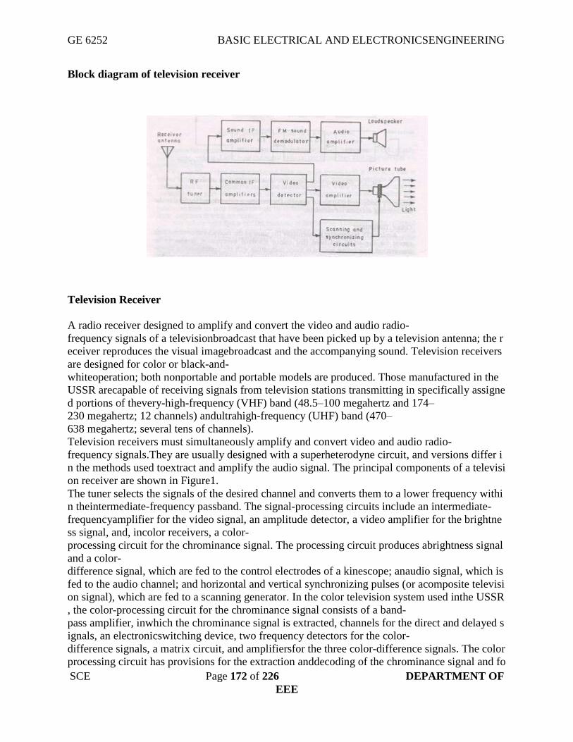
GE 6252 BASIC ELECTRICAL AND ELECTRONICSENGINEERING
SCE Page 172 of 226 DEPARTMENT OF
EEE
Block diagram of television receiver
Television Receiver
A radio receiver designed to amplify and convert the video and audio radio-
frequency signals of a televisionbroadcast that have been picked up by a television antenna; the r
eceiver reproduces the visual imagebroadcast and the accompanying sound. Television receivers
are designed for color or black-and-
whiteoperation; both nonportable and portable models are produced. Those manufactured in the
USSR arecapable of receiving signals from television stations transmitting in specifically assigne
d portions of thevery-high-frequency (VHF) band (48.5–100 megahertz and 174–
230 megahertz; 12 channels) andultrahigh-frequency (UHF) band (470–
638 megahertz; several tens of channels).
Television receivers must simultaneously amplify and convert video and audio radio-
frequency signals.They are usually designed with a superheterodyne circuit, and versions differ i
n the methods used toextract and amplify the audio signal. The principal components of a televisi
on receiver are shown in Figure1.
The tuner selects the signals of the desired channel and converts them to a lower frequency withi
n theintermediate-frequency passband. The signal-processing circuits include an intermediate-
frequencyamplifier for the video signal, an amplitude detector, a video amplifier for the brightne
ss signal, and, incolor receivers, a color-
processing circuit for the chrominance signal. The processing circuit produces abrightness signal
and a color-
difference signal, which are fed to the control electrodes of a kinescope; anaudio signal, which is
fed to the audio channel; and horizontal and vertical synchronizing pulses (or acomposite televisi
on signal), which are fed to a scanning generator. In the color television system used inthe USSR
, the color-processing circuit for the chrominance signal consists of a band-
pass amplifier, inwhich the chrominance signal is extracted, channels for the direct and delayed s
ignals, an electronicswitching device, two frequency detectors for the color-
difference signals, a matrix circuit, and amplifiersfor the three color-difference signals. The color
processing circuit has provisions for the extraction anddecoding of the chrominance signal and fo

GE 6252 BASIC ELECTRICAL AND ELECTRONICSENGINEERING
SCE Page 173 of 226 DEPARTMENT OF
EEE
r line selection, as well as chrominance disconnect circuits thatoperate when black-and-
white transmissions are received.
The scanning generators include horizontal and vertical scanning circuits that produce sawtooth c
urrentsin the horizontal and vertical scanning coils of the deflection system.
The high voltage for feeding thesecond anode of the kinescope is derived from a special
highvoltage winding of the line transformer or by rectifying pulses from the transformer; the volt
age for the focusing electrode is similarly derived.
The kinescope’s interface includes static and dynamic white balance controls, switches for exting
uishingthe electron guns, and regulators for focusing the beams. The demagnetizing circuit for a
color kinescopecreates a damped alternating current in a demagnetizing loop that circles the kine
scope screen. Thecurrent demagnetizes the shadow mask and tube rim, which are made of steel.
The audio section consists of an amplifier for the difference frequency, which in the USSR is 6.5
megahertz, a frequency detector for the audio signal, and a low-
frequency amplifier from which the audiosignal is fed to a high-
quality acoustical system, usually composed of several loudspeakers. The power-
supply section converts mains voltage into the supply voltages for all components of the televisio
n set,including the kinescope and vacuum tube heaters.
Microwave communication

GE 6252 BASIC ELECTRICAL AND ELECTRONICSENGINEERING
SCE Page 174 of 226 DEPARTMENT OF
EEE
Microwave transmission refers to the technology of transmitting information or energy by the
use ofelectromagnetic waves whose wavelengths are conveniently measured in small numbers of
centimetre; these are called microwaves. This part of the radio spectrum ranges
across frequencies of roughly 1.0 gigahertz (GHz) to 30 GHz. These correspond to wavelengths
from 30 centimeters down to 1.0 cm.
Microwaves are widely used for point-to-point communications because their
small wavelength allows conveniently-sized antennas to direct them in narrow beams, which can
be pointed directly at the receiving antenna. This allows nearby microwave equipment to use the
same frequencies without interfering with each other, as lower frequency radio waves do.
Another advantage is that the high frequency of microwaves gives the microwave band a very
large information-carrying capacity; the microwave band has a bandwidth 30 times that of all the
rest of the radio spectrum below it. A disadvantage is that microwaves are limited to line of
sight propagation; they cannot pass around hills or mountains as lower frequency radio waves
can.
Microwave radio transmission is commonly used in point-to-point communication systems on
the surface of the Earth, in satellite communications, and in deep space radio communications.
Other parts of the microwave radio band are used for radars, radio navigation systems, sensor
systems, and radio astronomy.
The next higher part of the radio electromagnetic spectrum, where the frequencies are above
30 GHz and below 100 GHz, are called "millimeter waves" because their wavelengths are
conveniently measured in millimeters, and their wavelengths range from 10 mm down to
3.0 mm. Radio waves in this band are usually strongly attenuated by the Earthly atmosphere and
particles contained in it, especially during wet weather. Also, in wide band of frequencies around
60 GHz, the radio waves are strongly attenuated by molecular oxygen in the atmosphere. The
electronic technologies needed in the millimeter wave band are also much more difficult to
utilize than those of the microwave band.

GE 6252 BASIC ELECTRICAL AND ELECTRONICSENGINEERING
SCE Page 175 of 226 DEPARTMENT OF
EEE
Satellite communication
A communications satellite or comsat is an artificial satellite sent to space for the purpose
oftelecommunications. Modern communications satellites use a variety of orbits
including geostationary orbits, Molniya orbits, elliptical orbits and low (polar and non-
polar) Earth orbits.
For fixed (point-to-point) services, communications satellites provide a microwave radio
relay technology complementary to that of communication cables. They are also used for mobile
applications such as communications to ships, vehicles, planes and hand-held terminals, and for
TV and radio broadcasting.
Communications Satellites are usually composed of the following subsystems:
Communication Payload, normally composed of transponders, antenna, and switching systems
Engines used to bring the satellite to its desired orbit
Station Keeping Tracking and stabilization subsystem used to keep the satellite in the right orbit,
with its antennas pointed in the right direction, and its power system pointed towards the sun
Power subsystem, used to power the Satellite systems, normally composed of solar cells, and
batteries that maintain power during solar eclipse
Command and Control subsystem, which maintains communications with ground control
stations. The ground control earth stations monitor the satellite performance and control its
functionality during various phases of its life-cycle.
The bandwidth available from a satellite depends upon the number of transponders provided by
the satellite. Each service (TV, Voice, Internet, radio) requires a different amount of bandwidth
for transmission. This is typically known as link budgeting and a network simulator can be used
to arrive at the exact value.

GE 6252 BASIC ELECTRICAL AND ELECTRONICSENGINEERING
SCE Page 176 of 226 DEPARTMENT OF
EEE
Optical fiber communication
Fiber-optic communication is a method of transmitting information from one place to another by
sending pulses of light through an optical fiber. The light forms an electromagnetic carrier
wave that ismodulated to carry information. First developed in the 1970s, fiber-
optic communication systems have revolutionized the telecommunications industry and have
played a major role in the advent of theInformation Age. Because of its advantages over
electrical transmission, optical fibers have largely replaced copper wire communications in core
networks in the developed world. Optical fiber is used by many telecommunications companies
to transmit telephone signals, Internet communication, and cable television signals. Researchers
at Bell Labs have reached internet speeds of over 100 petabits per second using fiber-optic
communication.
The process of communicating using fiber-optics involves the following basic steps: Creating the
optical signal involving the use of a transmitter, relaying the signal along the fiber, ensuring that
the signal does not become too distorted or weak, receiving the optical signal, and converting it
into an electrical signal.Optical fiber is used by many telecommunications companies to transmit
telephone signals, Internet communication, and cable television signals.
Due to much lower attenuation and interference, optical fiber has large advantages over existing
copper wire in long-distance and high-demand applications. However, infrastructure
development within cities was relatively difficult and time-consuming, and fiber-optic systems
were complex and expensive to install and operate. Due to these difficulties, fiber-optic
communication systems have primarily been installed in long-distance applications, where they
can be used to their full transmission capacity, offsetting the increased cost. Since 2000, the
prices for fiber-optic communications have dropped considerably. The price for rolling out fiber
to the home has currently become more cost-effective than that of rolling out a copper based
network. Prices have dropped to $850 per subscriber in the US and lower in countries like The
Netherlands, where digging costs are low and housing density is high.

GE 6252 BASIC ELECTRICAL AND ELECTRONICSENGINEERING
SCE Page 177 of 226 DEPARTMENT OF
EEE
GLOSSARY
A: symbol for ampere, the SI unit of current.
AC: literally, alternating current. Often used loosely to refer to other things which involve
alternating current; for example AC voltage probably means either alternating emf or
alternating potential difference.
Active device: a device which does something. It is nearly always a source of emf, but its
important property could be that it is sending a signal of some kind. (See also passive device.)
Active terminal: of a power point is the "live" or high potential (high voltage) terminal. The
neutral terminal is supposed to remain close to earth potential, but it may vary from that. See
also earth.
Alternating current: (AC) a current which is continually changing its value and direction in a
regular fashion. Usually it means a current which can be described by the equation: i = iosin(2p f
t) (a "sinusoidal" current) in which i is current, io is a constant called the amplitude of the
current, t is time and f is the frequency of the current. In Australia the frequency of commercially
generated AC power is 50 Hz, which means that the current changes direction 100 times per
second (twice for each cycle).
Ammeter: current meter; a contraction of ampere-meter.
Amp: colloquial name for ampere.
Amp hour: colloquial for ampere hour.
Ampere: the SI unit of electric current. Its symbol is A, so a current of 5 amperes is written as
5 A. A typical domestic appliance such as a toaster will carry a current of several amperes
Ampère, André-Marie: (1775-1836) French physicist who gave his name to the unit of current.
Ampere hour: a unit for describing the life of a battery which depends on how much current it
can produce for how long. Symbol A.h. A battery with a life of 1 A.h is nominally capable of
producing a current of 1 A for 1 h, or 0.5 A for 2 h, etc, before it goes flat. Since the product of
current and time has the dimensions of charge, it follows that if you run a battery with 1.00 A.h
capacity until it is flat, then 1 A.h or 3.6 ¥ 103 C of mobile charge will have passed through the
battery. You can estimate the energy that can be delivered from a battery by taking the product of
its life and its emf. For example a 2 V battery with a life of 5 A.h should be able to deliver about
(2 V) x (5 A.h) which equals 2 x 5 x 60 x 60 J or 7 kJ.
Analogue meter: a meter which is read by noting the position of a pointer against a scale.
Angular frequency: frequency multiplied by the number 2π. The "angular" bit is essentially a red
herring, but is related to the fact that an angle of 2π radians is one revolution. Usual
symbol: w (Greek lower-case omega). The SI unit is the reciprocal second, symbol s-1
, but some
folks, confused by the "angular" part of the name, use radian per second (rad.s-1
).
GE 6252 BASIC ELECTRICAL AND ELECTRONICSENGINEERING
SCE Page 178 of 226 DEPARTMENT OF
EEE
Battery: strictly a collection of electrochemical cells, but commonly refers also to a
single electrochemical cell. The key property of a battery or cell is its emf. For a battery
consisting of several cells, the total emf is equal to the sum of the cells' individual emfs.
C: the symbol for coulomb, the SI unit of charge. Not to be confused with the italic
symbol C for capacitance.
capacitance: property of a conductor or a pair of conductors which tells how good it is at
holding separated charge for a given potential (in the case of one conductor) or potential
difference for a pair of conductors. Defined as the quotient: charge divided by potential
(difference). The usual symbol is C (printed in italics in books - don't confuse it with the symbol
C for coulomb). The SI unit of capacitance is the farad.
Capacitor: a two-terminal device designed to have the property of capacitance. It usually
consists of two conducting objects separated by insulating material. It can also be thought of as a
device for storing energy.
Cell: see electrochemical cell, photovoltaic cell, charging.
Charge: the basic electrical property of matter. Usual symbol q, occasionally Q. There are two
kinds of charge which we call positive and negative. Of the particles which constitute atoms,
every proton has a positive charge of +e, every electron has a charge of -e, while neutrons have
no charge. (The value e is often called the electron charge rather than the proton charge because
the electron was discovered before the proton.) Normally the total charge of an atom is zero; the
number of protons in the nucleus is equal to the number of electrons in the atom; the atom is
electrically neutral. Charge does not exist independently of matter.
Charging: "charging" a battery is a misnomer for "energising" it. It means putting energy into
the battery by forcing a current through the battery, against the battery's emf. The
termcharging is misleading because the total charge in the battery is always the same; although
mobile charge passes through the battery during "charging" and "discharging" what matters is the
state of the chemicals in the battery and the energy that you can get from it.
Circuit: strictly, a circuit is just one conducting loop containing a string of electrical components
joined end to end. In common parlance the meaning is often extended to include any
arrangement of components, which may contain many different loops.
Circuit diagram: see schematic diagram.
Conductance: the opposite of resistance; a good conductor has a low resistance; defined as the
reciprocal of resistance or as the quotient, current through the object divided by the potential
difference across it. Usual symbol: G. The SI unit is the siemens, symbol S.
Conduction: the process by which charged particles move in an organised way through a
material thus forming a current.

GE 6252 BASIC ELECTRICAL AND ELECTRONICSENGINEERING
SCE Page 179 of 226 DEPARTMENT OF
EEE
Conductor: an electrical conductor is any thing or any material which can carry an
electric current. (In other contexts a conductor might be something that carries heat from one
place to another or a person who minds a travelling tram.) See also insulator, semiconductor.
Constant: steady, unchanging, having the same value during some interval of time. A constant
current (DC) does not change with time. See also uniform.
Conventional current: part of a model which supposes that current consists of moving positive
charge. Conventional current goes from the positive terminal of a battery, through a circuit and
back into the battery's negative terminal. Even though we know that for a metallic wire a better
model describes negatively charged electrons as carrying the current, the concept of conventional
current is well established and causes no problems in circuit theory. Unless a context tells you
otherwise, assume that all references to current mean conventional current.
Coulomb: the SI unit of charge, symbol C, named after Charles Augustin Coulomb (1736 -
1806) who formulated the law of interaction between charged particles. A coulomb of separated
charge is a huge quantity.
Current: an electric current is something that exists in a closed electrical circuit and is measured
using an ammeter. It is not the same as energy or voltage. The name is analogous with water
current in a river or an air current which is moving air. What moves in an electric current is
electrically charged particles, inside a conductor, whose total charge is zero or neutral. The usual
symbol is I; some books use i for changing current. The SI unit of current is the ampere (symbol
A). See also conventional current.
DC: literally, direct current, which usually means a steady unchanging current. DC is often
used as an adjective to refer to other things associated with direct current; for example DC
voltage usually means steady emf or steady potential difference.
Digital meter: a meter which displays its readings as numbers (digits).
Direct current: usually a constant current but the term could refer to a current with a constant
direction and a slowly changing value. A battery produces direct current.
Direction. Referring to circuits, direction does not mean direction in space but one of two
possible ways that you might trace out a circuit or part of a circuit. Such "directions" might be
described by terms such as "clockwise" or "from the positive terminal to the negative terminal".
To completely specify a current, you need to know its direction as well as its value.
Dynamic resistance: a property of a circuit component defined in terms of potential difference
(V) across the device and the current (i) through it as dV/di. It is not the same as resistance. For
devices which obey Ohm's law dynamic resistance is equal to resistance. The SI unit is the ohm,
symbol Ω.
Earth: literally just that, or a connection from a circuit to the earth - also called ground. It is
useful because the earth can be regarded as a good conductor, which provides a convenient path
for the completion of many circuits. Connection is usually made through a wire from the circuit
GE 6252 BASIC ELECTRICAL AND ELECTRONICSENGINEERING
SCE Page 180 of 226 DEPARTMENT OF
EEE
or apparatus to the earth; such a connection is always available through the earth pin of a
standard power point. (See also earth potential.)
Earth potential: for all practical purposes the earth always stays at the same potential, so it is a
convenient reference for specifying potentials, and it is conventionally assigned a potential of
zero volts. For example if you see a reference to a potential (rather than a potential difference) of
100 V, that means 100 V above earth potential.
Electricity: apart from being the name of the subject, electricity does not have a well-defined
technical meaning. How, then, should we translate common usages of the term? To 'generate
electricity' usually means to create emf, but when you 'buy electricity' you pay for energy. Some
people say that electricity means charge, but if you mean charge, it's probably better to
say charge.
Electromagnetic field: an electric field and a magnetic field together. Since electric and
magnetic fields are intimately linked to one another it makes sense to have a name which
indicates both together. Electromagnetic waves, including light, consist of electromagnetic fields.
electromagnetic induction: a process in which an emf is created either by moving a conductor
through a region containing a magnetic field, or by having a magnetic field which changes with
time. It is the process used to produce "electricity" (electrical energy) in power generators.
Electric field: a physical quantity which has a definite value at each point in space and which
determines amongst other things, the electrical force that would be experienced by a charged
particle at each point. We think of the field as existing in space even though there may be no
particle there to experience the force. Electric field is produced in two ways. (1) An electric field
exists in the space surrounding any charged particle. (2) An electric field is created by a
magnetic field which varies with time. The SI unit of electric field is the volt per metre, symbol
V.m-1.
Electron: type of fundamental particle which carries the smallest possible magnitude of a free
charge. The electron's charge is written symbolised as -e. The symbol e represents the value of
the fundamental charge: e = 1.60 ¥ 10-19 C. Electrons are constituents of all atoms and are the
charged particles which carry the current in a metallic wire.
emf: (pronounced "ee em eff") a physical quantity which describes the ability of an electrical
source to deliver energy. You can also think of it as the property of the source which creates
current in a circuit. Derived from the nineteenth century term "electromotive force" which is ok
(pronounced "okay") as far as the electromotive bit goes, but it is not a force as we define force
now. The emf of a battery is responsible for producing a potential difference between the
battery's terminals. If the battery is not connected to anything else, that potential difference is
equal to the emf. The SI unit is the volt, symbol V. [Not to be confused
with electromagnetic field which the popular press sometimes refers to as EMF.]
Energy: can't be easily defined. It is a physical quantity which, if you do the calculations
correctly, always gives the same total energy for the whole universe. Its meaning is best learned
through many examples, the same way that we learn normal language. It can be misleading to
GE 6252 BASIC ELECTRICAL AND ELECTRONICSENGINEERING
SCE Page 181 of 226 DEPARTMENT OF
EEE
think of energy as a kind of substance - it is more subtle than that. Energy is what you are asked
to pay for when you get your electricity bill. The SI unit of energy is the joule, symbol J.
Farad: the SI unit of capacitance, named after Michael Faraday, symbol F. One farad is a very
large capacitance; values of capacitors used in typical circuits are in the microfarad range (micro
= one millionth).
Faraday: an outmoded unit of charge, which we would now define as the charge of a mole of
protons, 96 406 coulombs
Faraday, Michael: (1791 - 1867) pioneer researcher in electricity and regarded as one of the all-
time greats of physics.
Frequency: the repetition rate for any process or phenomenon that repeats itself exactly; it is the
number of cycles divided by the total time interval taken. It is also equal to the reciprocal of
the period, the time taken for one complete cycle. Usual symbol: f. The SI unit of frequency is
the hertz, symbol Hz.
Ground: see earth.
Hertz: the SI unit of frequency, equivalent to one cycle per second; symbol Hz.
Impedance: a property of a circuit component, instrument or some other device which
encapsulates the relationship between the potential difference (PD) across the device and the
current through it.
Input: Literally something that is put in to something else or the cause of some effect which you
could call the output.
Insulator: any thing or type of material which is a very poor conductor of electricity. Electrical
wires (conductors) are covered on the outside with insulating material in order to guard against
accidental short circuits.
Internal resistance: is just resistance. The redundant "internal" is often added when one is
referring to something like a battery or an instrument.
J: symbol for joule, the SI unit of energy.
Joule: the SI unit of energy, symbol J. Named after English physicist James Prescott Joule (1818
- 1889) who helped to establish the concept of energy.
Kilowatt hour: non-SI unit of energy, used by electricity authorities for billing, equal to 3.6
megajoules. The symbol is kW.h, which is sometimes sloppily written as kWh.
kV: symbol for kilovolt, 103 V.

GE 6252 BASIC ELECTRICAL AND ELECTRONICSENGINEERING
SCE Page 182 of 226 DEPARTMENT OF
EEE
Load: something which takes electrical energy from a circuit. It is sometimes called an energy
sink. A household light globe becomes a load when it is connected to the mains and switched on.
mA: symbol for milliampere, 10-3
A.
Magnetic field: a physical quantity which has a definite value at each point in space. We think
of the field as existing in space even though there may be no particle there to experience the
force. Magnetic fields can be produced by magnets made of magnetic materials (iron in
particular), by electric currents and by electric fields which change with time. The SI unit of
magnetic field is the tesla, symbol T.
.
milliamp: colloquial for milliampere; one thousandth of an ampere. Symbol: mA.
multimeter: an instrument which can be used for measuring any one of several different
electrical quantities, usually potential difference (voltage), current and resistance. The user has
to select the quantity to be measured, by selecting some switch settings.
mV: symbol for millivolt, 10-3
V.
Negative: see positive and negative.
Neutral: (1) having zero net charge. The wires in a circuit remain neutral even though charged
electrons move inside them. (2) A different meaning occurs with the neutral wire or terminal in a
household wiring; in that case neutral means having near-zero potential - see under active
terminal.
Nominal value: literally "named value", usually a rough estimate of the intended value of
something. Nobody is too fussed when the real value turns out to be somewhat different.
ohm: SI unit of resistance; symbol Ω (the Greek letter, capital omega).
Ohm, Georg Simon: (1787 - 1854) German scientist who gave his name to the unit
of resistance.
Ohm's law: the statement that the resistance of some objects (notably metallic objects), held at
constant temperature, is independent of the potential difference across the object or the current
through it. There are many interesting objects which don't obey Ohm's law. Some people confuse
Ohm's law with the definition of resistance but an object can have a (variable) resistance, even
though it does not obey Ohm's law.
Open circuit: (1) a break in what was meant to be a circuit or (2) the broken circuit itself.
Turning a switch off creates an open circuit
Output: explained under input.

GE 6252 BASIC ELECTRICAL AND ELECTRONICSENGINEERING
SCE Page 183 of 226 DEPARTMENT OF
EEE
Parallel. Two components are in parallel if, when tracing a path between two points in a circuit,
you find that you have the alternative of branching off and tracing through either one component
or the other, before those alternative paths rejoin. Whether two things are in parallel or series
depends critically on the two points that you are tracing the path between; it makes no sense to
say that things are in parallel without reference to those points.
Passive device: a passive circuit component has no emf. The term comes from the idea that it
responds to something done to it by an active device, such as a battery. Light globes and
capacitors are passive devices.
Period: the time interval required for exactly one cycle of a repetitive process or phenomenon of
any kind. It is equal to the reciprocal of the process's frequency. Usual symbol, T. The SI unit is
the second, symbol s.
PD: lazy person's way of writing potential difference.
polarity: the property of a device which means that it has a positive terminal and a negative
terminal.
potential difference: difference in potential between two points in space.
power: rate of transfer of energy. For a steady rate (constant power) it can be expressed
as E/∆t where E is the energy transferred in the time interval ∆t. Usual symbol: P. The SI unit is
the watt (symbol W).
resistance: a property of an object associated with energy dissipation which occurs when
a current exists in the object.
resistor: a two-terminal device designed to have the property of resistance. It is usually desirable
that a resistor should obey Ohm's law and have a resistance that is fairly stable against
temperature changes. Most resistors are painted with a code consisting of coloured bands which
tell you the resistance.
semiconductor: a kind of material intermediate between a conductor and an insulator.
Semiconductors are used to make transistors, diodes and photovoltaic cells.
series. Circuit components are said to be connected in series with each other if they form a chain
without branches.
short circuit: a conducting path, or part of a circuit, with negligible or relatively low resistance.
The term is most commonly used to indicate an accidental path, which causes a much bigger
current than the one you wanted.
static resistance: exactly the same as resistance. The "static" qualifier is added in order to
emphasise that one does not mean dynamic resistance.
GE 6252 BASIC ELECTRICAL AND ELECTRONICSENGINEERING
SCE Page 184 of 226 DEPARTMENT OF
EEE
source: usually means a source or giver of electrical energy in a circuit, so it is a general term for
something that has an emf. It could also mean the source of a signal, but signal sources also have
emf. When current rather, than emf, is important one may refer to a current source, but a source
is still a source.
terminal: part of a component or a circuit to which something else gets connected. For example
a battery has two terminals both of which have to be joined into a circuit before you get anything
from the battery.
volt: the SI unit of potential, potential difference and emf, symbol V, named after
Alessandro Volta.
Volta, Alessandro: (1745 - 1827) Italian physicist who gave his name to lots of things electrical.
voltage: a colloquial term which could mean either emf or potential difference. It usually means
potential difference. If you know which one you mean it is better to use the more exact term.
voltmeter: an instrument for measuring potential difference. (It does not measure emf directly;
values of emf have to be inferred from other measurements.)
W: symbol for watt, the SI unit of power.
watt: the SI unit of power, symbol W, equivalent to 1 joule per second. Named after Scottish
engineer, James Watt (1736-1819).
work: energy which is transferred by any mechanism other than heat flow. Work is done on a
charged particle when it moves between two places with different potentials. A source ofemf can
increase the energy of a charged particle that passes through it. The SI unit is the joule, symbol J
Amplification: a method for increasing the amplitude (or loudness) of electrical signals
Amplifier: An electronic device which generates a high power signal based on the information
supplied by a lower powered signal. A perfect amplifier would add or subtract nothing from the
original except additional power - these have not been invented yet
CMOS: (Complementary Metal Oxide Semiconductor) - one family of digital logic devices.
Some CMOS devices can operate with power supplies from 3 Volts to 15 Volts - others are
limited to the traditional logic 5 Volt power supply.
Power Amp: An amplifier that is designed to drive loudspeakers or other relatively low
impedance loads. Usually combines voltage and current amplification. May be integrated with
the preamp (see below).
Semiconductor: Silicon (or various other materials) that are specially treated so as to form
diodes, transistors, MOSFETs, light emitting diodes (LEDs) etc. The basis of all modern
electronics.

GE 6252 BASIC ELECTRICAL AND ELECTRONICSENGINEERING
SCE Page 185 of 226 DEPARTMENT OF
EEE
Analogue to Digital Converter (ADC): A device that converts the infinite range of an analogue
signal into discrete "steps". Normally, a good audio ADC will use sufficient "steps" to resolve
the smallest musical detail. For CD, this is a 16 bit converter, having 65,536 discrete levels
covering the most negative signal level to the most positive
Binary: the basic counting system used in computer logic. Two values are available - 0 and 1. A
zero is normally represented by a 0 Volt signal, and a one by a voltage of approximately 5 Volts
- these levels are dependent upon the type of logic used
Binary Code: a coding scheme that communicates information by using a series of "1s" and
"Os" that are represented, respectively, by the digital "ON" and "OFF" states
Bit Stream: the bit rate, or flow of information, between a sender and receiver in digital
communication. Also called Digital Bit Stream.
Bit: a unit of the binary code that consists of either a single "1" or "O." (Commonly 5V or 0V
respectively.)
Byte: a unit of the binary code that consists of eight bits. One byte is required to code an
alphabetic or numeric character, using an eight-bit character set code.
CODEC: COder / DECoder - the component of any digital ssubsystem which performs analogue
to digital and digital to analogue conversions.
Digital/Analogue Conversion: a method used to recreate an analogue signal that has been coded
into binary data and transmitted as a digital signal.
Digital/Analogue Converter (DAC): a device used to generate a replica of the original
analogue signal that has been coded into binary data and transmitted as a digital signal.
Amplitude: the loudness of sound waves and electrical signals. Amplitude is measured in
decibels (dB) or volts
Attenuation: the decrease of a signal's amplitude level over any distance during transmission or
through purpose designed attenuators. Attenuation measures signal loss in decibels (dB)
Bandwidth: the measure of a range of frequencies containing an upper and lower limit
Cable: a type of linear transmission medium. Some of the common types of cables include: hook
up wire, coaxial (shielded) cables, lamp amd mains cable, figure-8 (zip) cable and fibre optics
Coaxial Cable: a metallic cable constructed in such a way that the inner conductor is shielded
from EMR (electromagnetic radiation) interference by the outer conductor. Coaxial cable is less
susceptible to more transmission impairments than twisted pair cable, and it has a much greater

GE 6252 BASIC ELECTRICAL AND ELECTRONICSENGINEERING
SCE Page 186 of 226 DEPARTMENT OF
EEE
bandwidth; thus coaxial cable is used by most analogue and digital systems for the transmission
of low level signals.
Crossover: A filter network which separates frequencies into "bands" which match the
capabilities of the loudspeaker drivers within an enclosure.
Crosstalk: a noise impairment when a signal from one pair of wires affects adjacent wires or one
channel affects the adjacent channel.
Cutoff Frequency: Normally defined as the frequency where the output from a filter has fallen
by 3dB from the maximum level obtainable through the filter.
Frequency: The rate at which an alternating current changes in a cyclic manner from positive to
negative and back again (one cycle). The basic unit of measurement is the Hertz (Hz), which
equates to one cycle per second.
Frequency Modulation (FM): a modulation technique that records changes in an information
signal by modifying the frequency of the carrier signal according to changes in the amplitude of
the information signal.

GE 6252 BASIC ELECTRICAL AND ELECTRONICSENGINEERING
SCE Page 187 of 226 DEPARTMENT OF
EEE
QUESTION BANK
UNIT I ELECTRICAL CIRCUITS & MEASUREMENTS
1. What is meant by charge?
Charge is an electrical property of the atomic particles which matter consists. The charge
of an electron is so small. Charge in motion represents current. The unit of charge is
coulomb.
2. What is meant by Current?
The flow of free electrons in a conductor is called current. Unit is ampere (A). I =
Q/t
3. What is meant by Voltage?
The poterntial difference between two points is called as voltage. Unit is Volts (V).
V=W/Q , W=work done in joules & Q = charge in coulombs
4. State Ohm’s Law.
The potential difference across any two ends of a conductor is directly proportional to
the current flowing between the two ends provided the temperature of the conductor remains
constant.
5. State Krichoff’s Voltage Law
KVL states that the algebraic sum of voltages in a closed path is zero.
6. State Krichoff’s current Law.
KCL states that the algebraic sum of currents in a node is zero.
7. Give short notes on resistor.
It is a property of a substance3 which opposes the flow of electrons. It is denoted by R
and its unit is Ohm
8. Distinguish between a Branch and a node of a circuit.
A pair of network which connects the various points of the network is called branch
A point at which two or more elements are joined together is called node.
9. Distinguish between a mesh and a loop of a circuit.
A mesh is a loop that does not contain other loops. All meshes are loop, but all loops are
not meshes. A loop is any closed path of branches
10. Write down the formula for a star connected network is converted into a delta
network?
RA=( R1 R2)/( R1 +R2+ R3)
RB=( R1 R3)/( R1 +R2+ R3)
RC=( R2 R3)/( R1 +R2+ R3)
GE 6252 BASIC ELECTRICAL AND ELECTRONICSENGINEERING
SCE Page 188 of 226 DEPARTMENT OF
EEE
11. Write down the formula for a delta connected network is converted into a star
network?
R1=( RARB+RBRC+RCRA)/RC
R2=( RARB+RBRC+RCRA)/RB
R3=( RARB+RBRC+RCRA)/RA
12. Define line currents and phase currents?
The currents flowing in the lines are called as line currents
The currents flowing through phase are called phase currents
13. Define line voltage and phase voltage?
The voltage across one phase and neutral is called line voltage & the voltage between two
lines is called phase voltage
14. Give the phase value & Line value of a star connected system.
VL= 3Vph
15. Give the phase value and line valued of a delta connected system.
IL= 3Iph
16. What is the power equation for a star connected system?
P= 3I V cosΦ L L W
17. What is the power equation for a delta connected system?
P= 3I V cosΦ L L W
18. What is meant by Real power?
Real power means the useful power transfer from source to load. Unit is watts.
19. What is meant by apparent power?
Apparent power is the product of voltage and current and it is not true power. Unit is VA
20. What is reactive power?
If we consider the circuit as purely inductive the output power is reactive power.
Its unit is VAR
21. Define Instrument.
Instrument is defined as a device for determining the value or magnitude of a quantity or
variable.
22. Mention the two main differences between an ammeter and a voltmeter.
Ammeter Voltmeter
It is a current measuring device it is a voltage measuring device
Always connected in series with circuit Always connected in parallel with circuit

GE 6252 BASIC ELECTRICAL AND ELECTRONICSENGINEERING
SCE Page 189 of 226 DEPARTMENT OF
EEE
The resistance is very small The resistance is very high
23. What is control system?
A system consists of a number of components connected together to perform a specific
function . In a system when the output quantity is controlled by varying the input quantity then
the system is called control system.
24. What are the two major types of control system?
The two major types of control system are open loop and closed loop
25. Define open loop control system.
The control system in which the output quantity has no effect upon the input quantity are
called open loop control system. This means that the output is not feedback to the input for
correction.
26. .Define closed loop control system.
The control system in which the output has an effect upon the input quantity so as to
maintain the desired output value are called closed loop control system
27. Mention the errors in Moving iron instruments.
Hysteresis error
Temperature error
Stray magnetic field error
Frequency error
Eddy current error
28. Mention any two precautions to be taken while using an Ammeter.
It should never be connected across any source.
The polarity must be observed correctly.
First use the highest range and then decrease the voltage range until the sufficient
deflection is obtained.
29. Define Form factor and Crest factor.
Form factor= RMS value / Average Value
Crest(peak) factor=Maximum Value / RMS value
30. Which type of instrument is called as universal instrument?
The moving iron instrument are known as universal instruments, because these
instruments can be used for AC and DC.
31. What are the applications of MI instruments?
i) Used as multirange ammeters and voltmeters.
ii) Used as in expensive indicators such as charging and discharging current indicators in
automobiles.

GE 6252 BASIC ELECTRICAL AND ELECTRONICSENGINEERING
SCE Page 190 of 226 DEPARTMENT OF
EEE
iii)Extensively used in industries for measurement of AC voltage and current where
errors of the order of 5% to 10% are accepetable.
32. What is meant by eddy current damping?
When the conductor moves in a magnetic field an emf is induced in it and if a closed path
is provided ,a current flows known as eddy current. This current intersect with the magnetic field
to produce an electromagnetic torque , which opposes the deflecting torque.
33. How is electrical power measured?
i) Using Voltmeter-ammeter method for DC circuits.
ii)Using Watt meters for AC circuits.
34. What do you mean by compensation coil in a wattmeter?
By connecting a compensating coil in series with a pressure coil, The error caused by the
pressure coil flowing in the current coil can be neutralized.
35. What are the three types of power used in a a.c circuit?
iii) Apparent power,S=EI
36. Define average value.
The average value of an alternating current is that value of steady direct current which
transfers the same charge as the alternating current flowing for the same time.
37. Define RMS value.
The effective value of an alternating current is that value of steady ,direct current which
produces the same heat as that produced by the alternating current when passed which produces
the same heat as that produced by the alternating current when passed through the same
resistance for the same interval of time.
38. Define reactive power.
The power consumed by a pure reactance (XL or Xc ) in a a.c circuit is called reactive
power. The unit is
PART B
1. Apply KCL and
KVL to the circuit
shown in fig.

GE 6252 BASIC ELECTRICAL AND ELECTRONICSENGINEERING
SCE Page 191 of 226 DEPARTMENT OF
EEE
2. Find the current through branch AB by using mesh current analysis
3. Find the current through 5 ohm resistance using mesh current analysis.
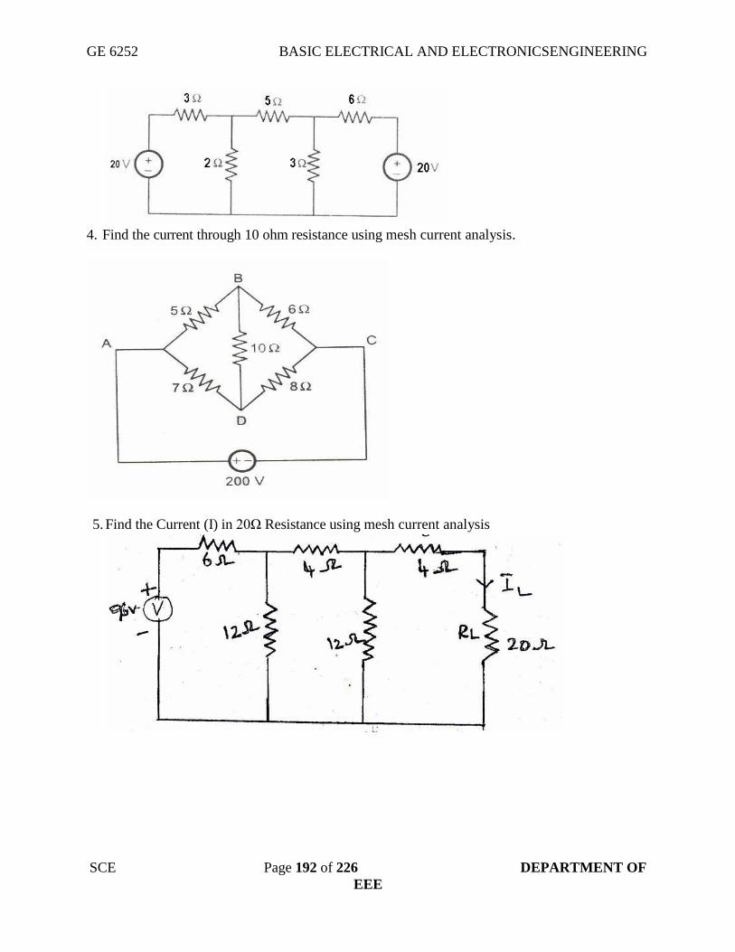
GE 6252 BASIC ELECTRICAL AND ELECTRONICSENGINEERING
SCE Page 192 of 226 DEPARTMENT OF
EEE
4. Find the current through 10 ohm resistance using mesh current analysis.
5. Find the Current (I) in 20Ω Resistance using mesh current analysis

GE 6252 BASIC ELECTRICAL AND ELECTRONICSENGINEERING
SCE Page 193 of 226 DEPARTMENT OF
EEE
6. Find the resistance between A & B , A & C
7. Consider the following network as shown in figure. Determine the power observed by the 6Ω .
8. Find the total Current and total Resistance in the circuit given

GE 6252 BASIC ELECTRICAL AND ELECTRONICSENGINEERING
SCE Page 194 of 226 DEPARTMENT OF
EEE
9. Derive the equation for given star network transformation in to delta network
10. Explain the construction and operation of moving coil instruments
11. Explain the construction and operation of moving iron repulsion type instruments
12. Explain the construction and operation of moving iron attraction type instruments
13. Explain the construction and operation of dynamo meter type watt meter
14. Explain the construction and operation of induction type single phase energy meter
UNIT II ELECTRICAL MECHANICS
1. What is an electric generator?
An electrical machine, which converts mechanical energy into electrical Energy, is called
as electric generator.
2. What is an electric motor?
An electrical machine, which converts electrical energy into mechanical Energy, is called
as electric motor.
3. What is meant by magnetic flux?
The magnetic lines of force existing around a magnet is called magnetic flux. It’s unit is
Weber.
4. State faraday’s law of electromagnetic induction.
Whenever a conductor cuts the magnetic lines of force an emf is induced in it.
5. State Fleming’s Right hand rule.
If three fingers of right hand, namely thumb, index finger and middle finger are
outstretched so that everyone of them is at right angles with the remaining two, and the index
finger is made to point in the direction of lines of flux, thumb in the direction of the relative
motion of the conductor and the middle finger gives the direction of the induced emf in the
conductor.
6.What is the use of commutator?
A device is used in a dc generator to convert the alternating emf into unidirectional emf is
called commutator.
7.What is the function yoke?
It serves the purpose of outermost cover of the dc machine. So that
the insulating material get protected from harmful atmospheric elements like moisture,
dust and various gases like SO2, acidic fumes etc.
It provides mechanical support to the poles.
8.What is the choice of material for the following?
1.Yoke 2.pole 3.Field winding 4.Armature winding
1.Yoke:

GE 6252 BASIC ELECTRICAL AND ELECTRONICSENGINEERING
SCE Page 195 of 226 DEPARTMENT OF
EEE
It is prepared by using cast iron because it is cheapest.
2.Pole:
It is made up of cast iron or cast steel.
3.Field winding:
It is made up of aluminium or copper.
4.Armatuer winding:
It is made up of cast iron or cast steel.
9.What is the function of brush?
To collect current from commutator and make it available to the stationary external
circuit.
10.Write down the emf equation for d.c generator.
Where
P = number of poles
Z = Total number of conductors
A = number of parallel paths
Ф = flux per pole
N = speed in rpm
11.What are all the two types of excitation?
i. Separate excitation
When the field winding is supplied from external, separate dc supply i.e.
Excitation of field winding is separate then the generator is called separately excited
generator.
ii. Self excitation
When the field winding is supplied from the armature of the generator itself then
it is called as self-excitation.
12.What is meant by residual magnetism?
Practically though the generator is not working, without any current through field
winding, the field poles posses some magnetic flux. This is called as residual magnetism.
13.Give the types of DC generator.
1.Self excited generator
Series Generator
Shunt Generator
Compound Generator
Long shunt compound generator
Short shunt compound generator
Cumulative and differential compound Generator
2. Separately excited generator
14.List out the applications of various types of generators.

GE 6252 BASIC ELECTRICAL AND ELECTRONICSENGINEERING
SCE Page 196 of 226 DEPARTMENT OF
EEE
Separately excited generator
As a separate supply is required to excite the field, the use is restricted to some special
applications like electroplating, electro refining of materials etc
Shunt generator
Commonly used in battery charging and ordinary lighting purposes.
Series Generators
Commonly used as boosters on dc feeders, as a constant current generators for welding generator
and arc lamps.
Cumulatively compound generators
These are used for domestic lighting purposes and to transmit energy over long distance.
Differential compound generator
The use of this type of generators is very rare and it is used for special application like electric
arc welding.
15.what is the principle of DC motor?
Whenever a current carrying conductor placed in a magnetic field, it experiences a
mechanical force.
16.State that the Fleming’s left hand rule.
The rules states that outstretch the three fingers of the left hand namely the first finger,
middle finger and thumb such that they are mutually perpendicular to each other. Now point the
first finger in the direction of magnetic field and the middle finger in the direction of the current
then the thumb gives the direction of the force experienced by the conductor.
17.What is Lenz’s law?
Lenz’s law states the direction of induced emf is always so as to oppose the cause
producing it.
18.Give the torque equation of a DC motor.
Ta=0.159fIa.PZ/A N-m
Ia - Armature current
P - Number of poles
Z - Total number of conductors
A -Number of parallel paths
19.List the different types of DC motor.
DC series motor
DC Shunt motor
DC Compound motor
Long shunt compound motor
Short shunt compound motor
20.List out the characteristics of DC motor.
i. Torque-Armature current characteristics (T VS Ia)
ii. Speed-Armature current characteristics (N VS Ia)

GE 6252 BASIC ELECTRICAL AND ELECTRONICSENGINEERING
SCE Page 197 of 226 DEPARTMENT OF
EEE
21.What are all the applications of DC motor?
DC Shunt motor:
Blowers and fans
Centrifugal and reciprocating pumps
Lathe machines
Machine tools
Milling machines
Drilling machines
DC Series motor:
Cranes
Hoists, Elevators
Trolleys,Conveyors,Electric locomotives
DC Cumulative compound motor:
Rolling mills
Punches
Shears
Heavy planers
Elevators
22. How is voltage generated in rotating machines?
In rotating machines voltage is generated in windings or group of coils by rotating them
through a magnetic field or by mechanically rotating a magnetic field past the winding or by
designing the magnetic circuit so that the reluctance varies with rotation of the rotor.
23.What is the basic principle of dc motor? A machine that converts dc power into mechanical power is known as a dc motor its
operation is based on the principle that when a current carrying conductor is placed in a magnetic
field, the conductor experiences a mechanical force. The direction of force is given by Fleming’s
left hand rule and magnitude is given by
F= BIL netwons.
Basically there is no constructional difference between a dc motor and dc generator.
The same dc machine can be run as a generator (or) motor.
24. What is back emf in d.c motors?
As the motor armature rotates, the system of conductor come across alternate North and
South pole magnetic fields causing an emf induced in the conductors. The direction of the emf
induced in the conductors. The direction of the emf induced is in the direction opposite to the
current .As this emf always opposes the flow of current in motor operation it is called back emf.
25. Mention the different parts of a d.c generator.
The different parts of dc generator are
(i) Magnetic frame (or) yoke.
(ii) pole core and pole shoes

GE 6252 BASIC ELECTRICAL AND ELECTRONICSENGINEERING
SCE Page 198 of 226 DEPARTMENT OF
EEE
(iii) pole coil or field coils
(iv) armature windings or conductors
(v) armature coils
(vi) commutator
(vii) Brushes and bearing.
26.What are the characteristics of DC generator? The characteristics of DC generator are
i) no load or saturation characteristics( Ea/ If)
ii) internal characteristics(E/If)
iii) external characteristics( V/If)
27.Write the various losses occurring in DC generator
Copper loss
Iron loss
Mechanical loss
28. Mention the difference between core and shell type transformers. In core type, the windings surround the core considerably and in shell type the core
surround the winding.
29. What is the purpose of laminating the core in a transformer? The purpose of laminating the core in a transformer is to reduce eddy current loss.
30. Give the emf equation of a transformer and define each term
Emf induced in primary coil E1 = 4.44 fΦ mN1 volt
Emf induced in secondary coil E2 = 4.44fΦ mN2 volt
Where f is the frequency of AC input Φ m is the maximum value of flux in the core N1,
N2 are the number of primary and secondary turns.
31.Define voltage regulation of a transformer
When a transformer is loaded with a constant primary voltage, the secondary voltage
decreases for lagging Power factor load, and increases for leading pf load because of its internal
resistance and leakage reactance. The change in secondary terminal voltage from no load to full
load expressed as a percentage of no loads or full load voltage is termed as regulation.
% regulation down = (0V2 -V2) x 100/0V2
% regulation up = (0V2 -V2) x 100/V2
32. Why transformers are rated in kVA?

GE 6252 BASIC ELECTRICAL AND ELECTRONICSENGINEERING
SCE Page 199 of 226 DEPARTMENT OF
EEE
Copper loss of a transformer depends on current and iron loss on voltage. Hence total
losses depend on Volt- Ampere and not on the power factor. That is why the rating of
transformers is in kVA and not in kW.
33. What are the typical uses of auto transformer?
(i) To give small boost to a distribution cable to correct for the voltage drop.
(ii) As induction motor starters.
(iii) As furnace transformers
(iv) As interconnecting transformers
(v) In control equipment for single phase and 3 phase elective locomotives.
34. When will a Bucholz relay operate in a transformer?
Bucholz rely is a protective device in a transformer.
If the temperature of the coil exceeds its limit, Bucholz relay operates and
gives an alarm.
35. Why are breathers used in transformers?
Breathers are used to entrap the atmospheric moisture and thereby not allowing it to pass
on to the transformer oil.
Also to permit the oil inside the tank to expand and contract as its temperature increases
and decreases.
36. What is the function of transformer oil in a transformer? Nowadays instead of natural mineral oil, synthetic oils known as ASKRELS (trade name)
are used. They are Noninflammable; under an electric arc do not decompose to produce
inflammable gases. PYROCOLOR oil possesses high dielectric strength.
Hence it can be said that transformer oil provides,
(i) good insulation and
(ii) cooling.
37. An 1100/400 V, 50 Hz single phase transformer has 100 turns on the secondary
winding. Calculate the number of turns on its primary. We know V1 / V2 = k = N2 / N1
Substituting 400/1100 = 100/N1
N1 = 100/400 x 1100 = 275 turns.
38. What are the functions of no-load current in a transformer?
No-load current produces flux and supplies iron loss and copper loss on no-load.
39. What is meant by a transformer?
The transformer is a static piece of apparatus by means of which electrical power is
transformed from one alternating current circuit to another with desired change in voltage and
current. Without any change in the frequency. It works on the principle of mutual induction

GE 6252 BASIC ELECTRICAL AND ELECTRONICSENGINEERING
SCE Page 200 of 226 DEPARTMENT OF
EEE
40. What are the advantages of a transformer?
i) Less I2R loss in the transmission line
ii) Less voltage drop in the line
iii) Efficiency of the transmission line is increased
iv) Volume of the conductor required is less.
41. What are the properties of ideal transformer? i) It has no loss
ii) Its winding have zero resistance.
iii) Leakage flux is zero i.e 100% flux produced by primary links with the secondary
iv) Permeability of core is so high that negligible current is required to establish the flues
is it.
42. What are the important parts of a transformer? Transformer consists of winding and magnetic core. The core is square or rectangle
shape. It consists of limb and yoke core is made up of lamination which is used to reduce eddy
current losses.
43. Define voltage transformation ratio? The ratio of secondary induced emf to primary induced emf is called as voltage
regulation ratio devoted by K.
44. Write the expression for equivalent resistance and reactance of transformer referred to
primary. Equivalent resistance Ro1 = R1 + R21 = R1 + R2/K2
Equivalent reactance Xo1 = X1 + X11 = X1 + X2/K2
45. Define voltage regulations of a transformer. The decrease in secondary terminal voltage expressed as a fraction of the no load
secondary terminal voltage is called voltage regulation of a transformer.
46. What are the losses occurring in a transformer? i) Core losses
ii) Copper losses
47. What is meant by core or iron losses?
Core or iron losses are caused as the core gets subjected to an alternating flux.
48. What is meant by hysteresis losses? Due to alternating flux set up in the magnetic core of the transformer, it undergoes a
cycle of magnetization and demagnetization.
GE 6252 BASIC ELECTRICAL AND ELECTRONICSENGINEERING
SCE Page 201 of 226 DEPARTMENT OF
EEE
Due to hysteresis effect there is loss of energy in this process which is called hysteresis
loss.
49. What is meant by copper loss? The copper losses are due to the power wasted in the form of I2R due to the resistances of
the primary and secondary windings.
50. What is meant by eddy current loss? The induced emf in the core tries to set up eddy currents in the core and hence
responsible for the eddy current losses.
51.Define all day efficiency? All day efficiency is the ratio energy (in kwh) delivered in a 24 hours period to the
energy (in kwh) input for the same length of time.
52. Define efficiency of a transformer?
The efficiency of a transformer is defined as the ratio of the output power to the input
power.
53. What is the function of capacitor in a single phase induction motor?
Capacitor is used to improve the power factor of the motor. Due to the capacitor
connected in series with the auxiliary winding, the capacitive circuit draws a leading current
which increases the split phase angle α between two phase currents Im and Ist.
54. What is the use of shading coil in the shaded pole motor? In shaded pole motors, the necessary phase-splitting is produced by induction. These
motors have salient poles on stator and a squirrel cage type rotor. The poles are shaded i.e.; each
pole carries a copper band one of its unequally divided part called shading band.
When single phase A.C. supply is given to the stator winding, due to shading provided to the
poles, a rotating magnetic field is generated.
55. Why capacitor-start induction motors advantageous? In capacitor-start induction motors, capacitor is connected in series with the auxiliary
winding. When speed of the motor approaches to 75 to 80% of the synchronous speed, the
starting winding gets disconnected due to the operation of the centrifugal switch. The capacitor
remains in the circuit only at start. The starting torque is proportional to phase angle α and hence
such motors produce very high starting torque.
56. List out four applications of shaded pole induction motor? Shaded pole motors have very low starting torque, low power factor and low efficiency.
These motors are commonly used for small fans, toy motors, advertising displays, film
projectors, record players, gramophones, hair dryers, photo copying machines etc.

GE 6252 BASIC ELECTRICAL AND ELECTRONICSENGINEERING
SCE Page 202 of 226 DEPARTMENT OF
EEE
57. What are the types of single phase induction motors? The types of single phase induction motors are:
1. Split phase induction motor.
2. Capacitor start induction motor.
3. Capacitor start and capacitor run motor.
4. Shaded pole induction motor.
PART B
1. Draw a neat sketch of a DC generator and label the component parts. Name the material used
for each component part.
2. Draw a constructional diagram for a generator and explain the parts dividually.
3. Explain different methods of excitation
4. Explain the different characteristics are available in DC series and DC shunt Generator.
5. Explain and derive the emf and torque equation .
6. Write the applications for different types of motors and generators
UNIT III SEMICONDUCTOR DEVICES AND APPLICATIONS
1) Define Transistor
Transistor consists of two junctions formed by sand witching either P-type or N-type
semiconductor between a pair of opposite types.
2). Write the current amplification factor for a CB transistor.
α = Change in Collector Current / at constant VCB
Change in emitter current
3) Write the formula for input resistance in a CB transistor
Input resistance = Change in base - emitter voltage /
Change in emitter current/at constant VCB
4). Write the current amplification factor for a CE transistor.
b = Change in Collector Current /
Change in base current at constant VCE
5). Define transistor action.
A transistor consists of 2 coupled PN junctions. The base is a common region to both
junctions and makes a coupling between them. Since the base regions are smaller, a significant
interaction between junctions will be available. This is called transistor actions.
6).Define delay time
It is defined as the time required for the current to rise from 0 to 10% of its maximum

GE 6252 BASIC ELECTRICAL AND ELECTRONICSENGINEERING
SCE Page 203 of 226 DEPARTMENT OF
EEE
value.
7). Define rise time
It is the time required for the current to rise from 0 to 90 percentage of the maximum
value.
8). Define turn-on time
It is the time required for the current to rise from 0 to 90 percentage of the maximum
value ton = td + tr
9).Define fall time
It is the time required for the Collector current to fall from 90 to 10 percentage of Ics.
10).Define Storage time
It is the time required to fall from 100 to 90 percent of Ics.
11).Define turn-off time
It is the time required to fall from 100 to 90 percent of Ics.
Toff=ts+tr
12).Define hybrid parameters.
Any linear circuit having input and output terminals can be analysed by four
parameters(one measured on ohm, one in mho and two dimensionless) called hybrid or
hparameters.
13). What are the use of h - Parameters?
It perfectly isolates the input and output circuits.
Its source and load currents are taken into account.
14).Define power transistors
Power transistors are those which handles a large amount of current and also dissipates
large amount of power across collector base junction.
15).Define current amplification factor in CC transistor.
g =Change in emitter current
Change in base current / at constant VCE
16 )Which is the most commonly used transistor configuration? Why?
The CE Configuration is most commonly used. The reasons are
High Current gain
High voltage gain
High power gain
Moderate input to output ratio.
17) What are the values of input resistance in CB, CE & CC Configuration

GE 6252 BASIC ELECTRICAL AND ELECTRONICSENGINEERING
SCE Page 204 of 226 DEPARTMENT OF
EEE
CB - Low about 75
CE - Medium About 750
CC - Very high about 750
18) Write the voltage and current equation for hybrid parameters.
V1 = h11i1 + h12V2
I2 = h21i1 + h22V2
19) What are the values of h-parameters?
h11 = V1/ i1
h12 = V1 / V2
h21 = i2 / i1
h22 = i2 / V2
20) h – parameter is applied to linear circuit True or False.
True
21) What are the advantages of transistors?
1.Low operating voltage.
2.Higher efficiency.
3.Small size and ruggedness
22) What are the types of transistors?
Unipolar junction transistor
Bipolar junction transistor.
23) What are the basic techniques used to construct a transistor?
Grown type.
Alloy type.
Electro chemically etched type
Diffusion type.
Epitaxial type.
24)What is mean by characteristics of transistor?
The interrelation of the various currents and voltages can be plotted graphically which are
commonly known as the characteristics of transistor.
25)What are the types of BJT?
n-p-n type.
p-n-p type.

GE 6252 BASIC ELECTRICAL AND ELECTRONICSENGINEERING
SCE Page 205 of 226 DEPARTMENT OF
EEE
PART B
1. Explain the working of NPN transistor
2. Explain the working of PNP transistor
3. Explain the current components of the transistor
4. What are the basic techniques used for the construction of a transistor?
5. Explain the common base configuration.
6. Draw the hybrid model for CE configuration
UNIT IV DIGITAL ELECTRONICS
1) Given the two binary numbers X = 1010100 and Y = 1000011, perform the subtraction (a)
X -Y and (b) Y - X using 2's complements.
a) X = 1010100
2's complement of Y = + 0111101
--------------
Sum = 10010001
Discard end carry
Answer: X - Y = 0010001
b) Y = 1000011
2's complement of X = + 0101100
---------------
Sum = 1101111
There is no end carry,
Therefore the answer is Y-X = -(2's complement of 1101111) = -0010001

GE 6252 BASIC ELECTRICAL AND ELECTRONICSENGINEERING
SCE Page 206 of 226 DEPARTMENT OF
EEE
2). Given the two binary numbers X = 1010100 and Y = 1000011, perform the subtraction
(a) X -Y and (b) Y - X using 1's complements.
a). X - Y = 1010100 - 1000011
X = 1010100
1's complement of Y = + 0111100
--------------
Sum = 10010000
End -around carry = + 1
--------------
Answer: X - Y = 0010001
b). Y - X = 1000011 - 1010100
Y = 1000011
1's complement of X = + 0101011
-----------
Sum = + 1101110
There is no end carry.
Therefore the answer is Y - X = -(1's complement of 1101110) = -0010001
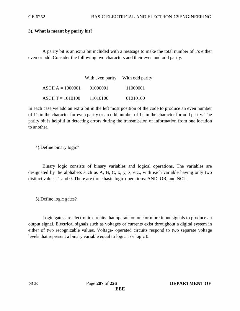
GE 6252 BASIC ELECTRICAL AND ELECTRONICSENGINEERING
SCE Page 207 of 226 DEPARTMENT OF
EEE
3). What is meant by parity bit?
A parity bit is an extra bit included with a message to make the total number of 1's either
even or odd. Consider the following two characters and their even and odd parity:
With even parity With odd parity
ASCII A = 1000001 01000001 11000001
ASCII T = 1010100 11010100 01010100
In each case we add an extra bit in the left most position of the code to produce an even number
of 1's in the character for even parity or an odd number of 1's in the character for odd parity. The
parity bit is helpful in detecting errors during the transmission of information from one location
to another.
4).Define binary logic?
Binary logic consists of binary variables and logical operations. The variables are
designated by the alphabets such as A, B, C, x, y, z, etc., with each variable having only two
distinct values: 1 and 0. There are three basic logic operations: AND, OR, and NOT.
5).Define logic gates?
Logic gates are electronic circuits that operate on one or more input signals to produce an
output signal. Electrical signals such as voltages or currents exist throughout a digital system in
either of two recognizable values. Voltage- operated circuits respond to two separate voltage
levels that represent a binary variable equal to logic 1 or logic 0.

GE 6252 BASIC ELECTRICAL AND ELECTRONICSENGINEERING
SCE Page 208 of 226 DEPARTMENT OF
EEE
6).Define duality property.
Duality property states that every algebraic expression deducible from the postulates of
Boolean algebra remains valid if the operators and identity elements are interchanged. If the dual
of an algebraic expression is desired, we simply interchange OR and AND operators and replace
1's by 0's and 0's by 1's.
7).Find the complement of the functions F1 = x'yz' + x'y'z and F2 = x(y'z' + yz). By applying
De Morgan's theorem as many times as necessary.
F1' = (x'yz' + x'y'z)' = (x'yz')'(x'y'z)' = (x + y' + z)(x + y +z')
F2' = [x(y'z' + yz)]' = x' + (y'z' + yz)'
= x' + (y'z')'(yz)'
= x' + (y + z)(y' + z')
8).Find the complements of the functions F1 = x'yz' + x'y'z and F2 = x(y'z' + yz). by taking
their duals and complementing each literal.
F1 = x'yz' + x'y'z
The dual of F1 is (x' + y + z')(x' + y' + z)
Complementing each literal: (x + y' + z)(x + y + z')
F2 = x(y'z' + yz).
The dual of F2 is x + (y' + z')(y + z).
Complement of each literal: x' + (y + z)(y' + z')
9).State De Morgan's theorem.
De Morgan suggested two theorems that form important part of Boolean algebra. They are,

GE 6252 BASIC ELECTRICAL AND ELECTRONICSENGINEERING
SCE Page 209 of 226 DEPARTMENT OF
EEE
1) The complement of a product is equal to the sum of the complements.
(AB)' = A' + B'
2) The complement of a sum term is equal to the product of the complements.
(A + B)' = A'B'
10).Reduce A.A'C
A.A'C = 0.c [A.A' = 1]
= 0
11). Reduce A(A + B)
A(A + B) = AA + AB
= A(1 + B) [1 + B = 1]
= A.
12. Reduce A'B'C' + A'BC' + A'BC
A'B'C' + A'BC' + A'BC = A'C'(B' + B) + A'B'C
= A'C' + A'BC [A + A' = 1]
= A'(C' + BC)
= A'(C' + B) [A + A'B = A + B]
13.) Reduce AB + (AC)' + AB'C(AB + C)

GE 6252 BASIC ELECTRICAL AND ELECTRONICSENGINEERING
SCE Page 210 of 226 DEPARTMENT OF
EEE
AB + (AC)' + AB'C(AB + C) = AB + (AC)' + AAB'BC + AB'CC
= AB + (AC)' + AB'CC [A.A' = 0]
= AB + (AC)' + AB'C [A.A = 1]
= AB + A' + C' =AB'C [(AB)' = A' + B']
= A' + B + C' + AB'C [A + AB' = A + B]
= A' + B'C + B + C' [A + A'B = A + B]
= A' + B + C' + B'C
=A' + B + C' + B'
=A' + C' + 1
= 1 [A + 1 =1]
14. Simplify the following expression Y = (A + B)(A + C' )(B' + C' )
Y = (A + B)(A + C' )(B' + C' )
= (AA' + AC +A'B +BC )(B' + C') [A.A' = 0]
= (AC + A'B + BC)(B' + C' )
= AB'C + ACC' + A'BB' + A'BC' + BB'C + BCC'
= AB'C + A'BC'
15).Simplify the following using De Morgan's theorem [((AB)'C)'' D]'
[((AB)'C)'' D]' = ((AB)'C)'' + D' [(AB)' = A' + B']
= (AB)' C + D'
= (A' + B' )C + D'
16.Show that (X + Y' + XY)( X + Y')(X'Y) = 0

GE 6252 BASIC ELECTRICAL AND ELECTRONICSENGINEERING
SCE Page 211 of 226 DEPARTMENT OF
EEE
(X + Y' + XY)( X + Y')(X'Y) = (X + Y' + X)(X + Y' )(X' + Y) [A + A'B = A + B]
= (X + Y' )(X + Y' )(X'Y) [A + A = 1]
= (X + Y' )(X'Y) [A.A = 1]
= X.X' + Y'.X'.Y
= 0 [A.A' = 0]
17).Prove that ABC + ABC' + AB'C + A'BC = AB + AC + BC
ABC + ABC' + AB'C + A'BC =AB(C + C') + AB'C + A'BC
=AB + AB'C + A'BC
=A(B + B'C) + A'BC
=A(B + C) + A'BC
=AB + AC + A'BC
=B(A + C) + AC
=AB + BC + AC
=AB + AC +BC ...Proved
18).Convert the given expression in canonical SOP form Y = AC + AB + BC
Y = AC + AB + BC
=AC(B + B' ) + AB(C + C' ) + (A + A')BC
=ABC + ABC' + AB'C + AB'C' + ABC + ABC' + ABC
=ABC + ABC' +AB'C + AB'C' [A + A =1]
19).Convert the given expression in canonical POS form Y = ( A + B)(B + C)(A + C)

GE 6252 BASIC ELECTRICAL AND ELECTRONICSENGINEERING
SCE Page 212 of 226 DEPARTMENT OF
EEE
Y = ( A + B)(B + C)(A + C)
= (A + B + C.C' )(B + C + A.A' )(A + B.B' + C)
= (A + B + C)(A + B + C' )(A + B +C)(A' + B +C)(A + B + C)(A + B' +
C)
[A + BC = (A + B)(A + C) (Distributive law]
= (A + B + C)(A + B + C')(A' + B + C)(A' + B + C)(A + B' + C)
20) Write down the steps in implementing a Boolean function with levels of NAND Gates?
Simplify the function and express it in sum of products.
Draw a NAND gate for each product term of the expression that has at least two literals.
The inputs to each NAND gate are the literals of the term. This constitutes a group of first level
gates. Draw a single gate using the AND-invert or the invert-OR graphic symbol in the second
level, with inputs coming from outputs of first level gates.
A term with a single literal requires an inverter in the first level. How ever if the single
literal is complemented, it can be connected directly to an input of the second level NAND gate.
21) Give the general procedure for converting a Boolean expression in to multilevel NAND
diagram?
Draw the AND-OR diagram of the Boolean expression.
Convert all AND gates to NAND gates with AND-invert graphic symbols.
Convert all OR gates to NAND gates with invert-OR graphic symbols.
Check all the bubbles in the same diagram. For every bubble that is not compensated by
another circle along the same line, insert an inverter or complement the input literal.

GE 6252 BASIC ELECTRICAL AND ELECTRONICSENGINEERING
SCE Page 213 of 226 DEPARTMENT OF
EEE
22) What are combinational circuits?
A combinational circuit consists of logic gates whose outputs at any time are determined
from the present combination of inputs. A combinational circuit performs an operation that can
be specified logically by a set of Boolean functions. It consists of input variables, logic gates,
and output variables.
23) Give the design procedures for the designing of a combinational circuit.
The procedure involves the following steps,
From the specification of the circuit, determine the required number of inputs and outputs
and assign a symbol to each.
Derive the truth table that defines the required relationships between inputs and outputs.
Obtain the simplified Boolean functions for each output as a function of the input
variables.
Draw the logic diagram and verify the correctness of the design.
24) Define half adder.
A combinational circuit that performs the addition of two bits is called a half adder. A half
adder needs two binary inputs and two binary outputs. The input variables designate the augend
and addend bits; the output variables produce the sum and carry
25) Define full adder?
A combinational circuit that performs the adtion of three bits is a full adder.It consists of
three inputs and two outputs.
The carry into sign bit position and the carry out of the sign bit position. If these two
carries are not equal, an overflow has occurred.
26. Represent binary number 1101 - 101 in power of 2 and find its decimal equivalent
N = 1 x 2 3 + 1 x 2 2 + 0 x 2 1 + 1 x 2 0 + 1 x 2 -1 + 0 x 2 -2 + 1 x 2 -3
= 13.625 10
27. What are the different classification of binary codes?
1. Weighted codes
2. Non - weighted codes

GE 6252 BASIC ELECTRICAL AND ELECTRONICSENGINEERING
SCE Page 214 of 226 DEPARTMENT OF
EEE
3. Reflective codes
. Sequential codes
5. Alphanumeric codes
6. Error Detecting and correcting codes.
28. Write the names of basic logical operators.
1. NOT / INVERT
2. AND
3. OR
29. Simplify the following expression
y = (A + B) (A = C) (B + C)
= (A A + A C + A B + B C) (B + C)
= (A C + A B + B C) (B + C)
= A B C + A C C + A B B + A B C + B B C + B C C
= A B C = A B C
30. Show that the NAND connection is not associative
The NAND connection is not associative says that
A . B . C A . B. C
A . B + C A + B C
AB + C A + BC
31. What is a Logic gate?
Logic gates are the basic elements that make up a digital system. The electronic gate is a
circuit that is able to operate on a number of binary inputs in order to perform a particular
logical function.
32. Write the names of Universal gates.
1. NAND gate
2. NOR gate
GE 6252 BASIC ELECTRICAL AND ELECTRONICSENGINEERING
SCE Page 215 of 226 DEPARTMENT OF
EEE
33. Why are NAND and NOR gates known as universal gates?
The NAND and NOR gates are known as universal gates, since any logic function
can be implemented using NAND or NOR gates.
34. Define combinational logic
When logic gates are connected together to produce a specified output for certain
specified combinations of input variables, with no storage involved, the resulting
circuit is called combinational logic.
35. Explain the design procedure for combinational circuits
¢ The problem definition
¢ The determination of number of available input variables & required O/P
variables.
¢ Assigning letter symbols to I/O variables
¢ Obtain simplified boolean expression for each O/P.
¢ Obtain the logic diagram.
36. Define half adder and full adder
The logic circuit which performs the addition of two bits is a half adder.
The circuit which performs the addition of three bits is a full adder.
PART – B 1. a. Write the verilog code generate for parallel load up / down
Counter b. Write a verilog code for D Flip Flop and R-S Flip Flop
2. Explain R-S Flip Flop and Clocked R-S Flip Flop
3 .a. Explain S-R Flip Flop
b. Explain D Flip Flop
4. a. Explain JK Flip Flop
b. Explain T Flip Flop
5.a. Explain Master Slave Flip Flop
b. Explain the Edge Triggered Flip Flop
6. a. Convert it JK Flip Flop in to T Flip Flop
b. Convert it JK Flip Flop in to D Flip Flop
GE 6252 BASIC ELECTRICAL AND ELECTRONICSENGINEERING
SCE Page 216 of 226 DEPARTMENT OF
EEE
7. a. Convert it D Flip Flop in to T Flip Flop
b. Convert it T Flip Flop in to D Flip Flop
8. a. Explain Serial in Serial out Shift Register
b. Explain Serial in parallel out Shift Register
9. a. Explain parallel in parallel out Shift Register
b. Explain parallel in Serial out Shift Register
10. Design sequential circuit for a state diagram?
UNIT V FUNDAMENTALS OF COMMUNICATION ENGINEERING
1. What do you mean by radio communication? Ans. The process sending audio signal from a source to distant destination using carrier wave is
called radio communication.
2. Explain communication system with the help of block diagram? Source destination
3.Wite name of sub units of radio communication system? i. Transmitters
ii. Transmission Channel
iii. Receiver
4 What do you understand by modulation? Ans. The process of varying one of the characteristics of a high frequency wave ai accordance
with the instantaneous value of a low frequency signal is called modulation.
5 What is modulating wave? Ans. Low frequency signal is called modulating wave.
6 What is carrier wave?
Ans. High frequency wave is called carrier wave.
7 What are different types of modulation? Ans. i. Amplitude modulation (AM)
ii. Frequency Modulation (FM)
iii. Phase modulation (PM)
8 Give the definition of Amplitude modulation (AM)? Ans . Amplitude modulation (AM) is a technique used in electronic communication, most
commonly for transmitting information via a radio carrier wave. AM works by varying the
strength of the transmitted signal in relation to the information being sent.
9 Give the definition of Frequency Modulation (FM).

GE 6252 BASIC ELECTRICAL AND ELECTRONICSENGINEERING
SCE Page 217 of 226 DEPARTMENT OF
EEE
Ans. Frequency modulation (FM) conveys information over a carrier wave by varying its
instantaneous frequency in accordance with the frequency of the carrier wave.
10 What is modulation index?
Ans. Modulation index of amplitude modulation is defined as the ratio of the amplitude of the
modulating wave to the amplitude of the carrier wave
11 what are the disadvantages of AM?
i. Smaller operating range
ii. Poor audio Quality
iii. Low Efficiency
iv. Reception noisy
12 What are the advantages of FM? Ans.
i. Noiseless Reception
ii. Better Quality
iii. High operating range
iv. Efficiency is very high
13. What are the disadvantages of FM? Ans. i. Costly equipments
ii. Smaller area of reception
iii.Much wider channel is required
14. What is demodulation? Ans. The process of recovering the audio signal from modulated wave is known as
demodulation. Or detection. Thus demodulation is reverse process of modulation .
15 Give the definition of phase modulation (PM)? Ans. In this he phase of the carrier wave is varied in accordance with the instantaneous value of
modulating signal.
16 What GSM and CDMA stands for? Ans. GSM stands for Global system for mobile communication.
CDMA stands for Code division multiple access.
17 What do you understand by the term television.
Ans. Television (TV) is the most widely used telecommunication medium for transmitting and
receiving moving images that are either monochromatic ("black and white") or color, usually
accompanied by sound. "Television" may also refer specifically to a television set, television
programming or television transmission.

GE 6252 BASIC ELECTRICAL AND ELECTRONICSENGINEERING
SCE Page 218 of 226 DEPARTMENT OF
EEE
18 Determine the size of antenna working at frequency of 20 kHz and wave length of wave
1.5*106 m given that velocity of light to be3*108 m/s . Ans. λ = c/f
= 3*108 m/s/20*103 = 15*103 m
Size of antenna = λ/4 = 3750 m. ans.
19 What is super heterodyne radio receiver ? Ans. It is an improved radio receiver which employs the principle of heterodyning (means
frequency translation
20. What is the basic principle of communication satellites? Ans. communication satellites has uplink and down link frequency and used for various research
works and weather forecasting.
PART-B
1. What do you understand by the term communication systems?
2.What is Modulation and why it is needed?
3.What are the types of modulation?
4.Deduce the expression for modulation index for AM.
5.Explain the advantages of FM over AM.
6.Derive the expression for modulation index or index of modulation for FM?
7. Determine the size of antenna working at frequency of 20 kHz and wave length of wave
2.5*106 m given that velocity of light to be 3*108 m/s .Comment on the result
obtained.
8. Explain the principle of mobile communication .
9. How communication satellites work?
10. Briefly explain the working of super heterodyne radio receiver with the help of block
diagram
11. Briefly discuss the principle of mobile communication?
12. What do you understand by Multiple-Access Techniques?

GE 6252 BASIC ELECTRICAL AND ELECTRONICSENGINEERING
SCE Page 219 of 226 DEPARTMENT OF
EEE

GE 6252 BASIC ELECTRICAL AND ELECTRONICSENGINEERING
SCE Page 220 of 226 DEPARTMENT OF
EEE

GE 6252 BASIC ELECTRICAL AND ELECTRONICSENGINEERING
SCE Page 221 of 226 DEPARTMENT OF
EEE

GE 6252 BASIC ELECTRICAL AND ELECTRONICSENGINEERING
SCE Page 222 of 226 DEPARTMENT OF
EEE

GE 6252 BASIC ELECTRICAL AND ELECTRONICSENGINEERING
SCE Page 223 of 226 DEPARTMENT OF
EEE

GE 6252 BASIC ELECTRICAL AND ELECTRONICSENGINEERING
SCE Page 224 of 226 DEPARTMENT OF
EEE

GE 6252 BASIC ELECTRICAL AND ELECTRONICSENGINEERING
SCE Page 225 of 226 DEPARTMENT OF
EEE
GE 6252 BASIC ELECTRICAL AND ELECTRONICSENGINEERING
SCE Page 226 of 226 DEPARTMENT OF
EEE