gaussian thermionic emission model for analysis of au/mos2
TRANSCRIPT
PHYSICAL REVIEW APPLIED 14, 054027 (2020)
Gaussian Thermionic Emission Model for Analysis of Au/MoS2 Schottky-BarrierDevices
Calvin Pei Yu Wong ,1,2,3,* Cedric Troadec ,2 Andrew T.S. Wee ,1,2 andKuan Eng Johnson Goh 2,3,†
1NUS Graduate School for Integrative Sciences and Engineering, National University of Singapore, Centre for
Life Sciences, #05-01, 28 Medical Drive, Singapore 117456, Singapore2Institute of Materials Research and Engineering, A*STAR (Agency for Science, Technology and Research), 2
Fusionopolis Way, #08-03 Innovis, Singapore 138634, Singapore3Department of Physics, Faculty of Science, National University of Singapore, 2 Science Drive 3, Singapore
117551, Singapore
(Received 9 August 2020; revised 17 September 2020; accepted 21 September 2020; published 12 November 2020)
Schottky-barrier inhomogeneities are expected at the metal–transition-metal-dichalcogenide (TMDC)interface and this can impact device performance. However, it is difficult to account for the distribution ofinterface inhomogeneity as most techniques average over the spot area of the analytical tool (e.g., few hun-dred micrometers squared for photoelectron-based techniques), or the entire device measured for electricalcurrent-voltage (I-V) measurements. Commonly used models to extract Schottky-barrier heights neglector fail to account for such inhomogeneities, which can lead to the extraction of incorrect Schottky-barrierheights and Richardson constants that are orders of magnitude away from theoretically expected values.Here, we show that a Gaussian-modified thermionic emission model gives the best fit to experimentaltemperature-dependent current-voltage (I-V-T) data of van der Waals Au/p-MoS2 interfaces and allow thedeconvolution of the Schottky-barrier heights of the defective regions from the pristine region. By theinclusion of a Gaussian-distributed Schottky-barrier height in the macroscopic I-V-T analysis, we demon-strate that interface inhomogeneities due to defects are deconvoluted and well correlated to the impact onthe device behavior across a wide temperature range from a room temperature of 300 K down to 120 K.We verify the Gaussian thermionic model across two different types of p-MoS2 (geological bulk crystalsand synthetic flux-grown crystals), and finally compare the macroscopic Schottky-barrier heights with theresults of a nanoscopic technique, ballistic hole emission microscopy (BHEM). The results obtained usingBHEM are consistent with the pristine Au/p-MoS2 Schottky-barrier height extracted from the Gaussian-modified thermionic emission model over hundreds of nanometers. Our findings show that the inclusion ofSchottky-barrier inhomogeneities in the analysis of I-V-T data is useful to elucidate the impact of defects(e.g., grain boundaries, metallic impurities, etc.) and hence their influence on device behavior. We alsofind that the effective Richardson constant, a material-specific constant typically treated as merely a fittingconstant, is a useful parameter to check for the validity of the transport model.
DOI: 10.1103/PhysRevApplied.14.054027
I. INTRODUCTION
Schottky-barrier inhomogeneities are present at themetal–transition-metal-dichalcogenide (TMDC) interfacedue to potential fluctuations and defects in the material andthis can impact the device performance [1–4]. However,the most commonly used thermionic emission transport
*[email protected]†[email protected]
Published by the American Physical Society under the terms ofthe Creative Commons Attribution 4.0 International license. Fur-ther distribution of this work must maintain attribution to theauthor(s) and the published article’s title, journal citation, andDOI.
model modified with a simple ideality factor correction[5] does not account sufficiently for nonideal effects suchas inhomogeneities, often leading to the extraction of anapparent Schottky-barrier height (SBH) convoluted withother factors such as defects (inhomogeneity) and temper-ature. The extracted apparent SBH from the simple modeldoes not represent the true band alignment at the metal-semiconductor interface and is counterproductive to thecorrect understanding of the energetics of the interface.Several other models have been proposed to account forthese nonideal effects in the current-voltage (I-V) behav-ior of Schottky-barrier devices [1–8]. In this paper, wecompare the effectiveness of four types of commonly usedtransport models to extract correct values of the SBH andthe material-specific Richardson constant of MoS2. We
2331-7019/20/14(5)/054027(15) 054027-1 Published by the American Physical Society
WONG, TROADEC, WEE, and GOH PHYS. REV. APPLIED 14, 054027 (2020)
verify the SBH extracted from the transport models againstthe SBH obtained from ballistic hole emission microscopy(BHEM) [9–11], which is a direct measurement methodfor the SBH at the nanoscale, and verify the Richard-son constants extracted from the models with theoreticalcalculated values based on the electron (hole) effectivemass of MoS2 [12,13]. Finally, we compare the SBH andRichardson constants across two types of MoS2 (geolog-ical bulk crystals and synthetic flux grown bulk crystals)from different sources and show that the SBH and Richard-son constants are similar across the two MoS2 devices ifanalyzed using the correct model.
The transport of thermally activated carriers across atypical metal-semiconductor Schottky interface where thesemiconductor is lightly doped (approximately 1015 to1017 cm−3) is given by the ideal thermionic emissionmodel [Eq. (1)] [5].
I = IS
[exp
(qVkT
)− 1
], (1)
where
IS =[
AA∗∗T2 exp(
−qφ
kT
)](2)
and q is the electric charge, V the voltage applied across thediode, k the Boltzmann constant, T the absolute tempera-ture, A the area of the diode, A** the effective Richardsonconstant of the semiconductor, and φ the Schottky-barrierheight. A requirement of this model is that the tunnel-ing of carriers across the Schottky barrier is negligible,which is valid when the semiconductor is lightly doped(approximately 1015 to 1017 cm−3) such that the bandbanding is gradual and the Schottky-barrier width is wide.The accurate extraction of the SBH depends greatly onthe successful determination of IS from the forward-biasslope of the experimental I-V curves [Eq. (1)]. How-ever, the thermionic emission model does not fit wellto experimental I -V curves at low temperatures, and themodified (nonideal) thermionic emission models [6,7], thethermionic field emission (thermally assisted tunneling)model or the generation-recombination model are oftenused instead [14,15]. While these modified models seemto fit certain experimental datasets well, the numbers thathave been extracted have not always been reliable. Forinstance, negative SBHs have been reported [16,17], butnegative SBHs have no physical meaning and show thatthe models are not suitable for these specific devices, andother material-specific constants such as the Richardsonconstants are orders of magnitude away from the theo-retically derived values [6,7]. Hence, it is not trivial toidentify a correct model to accurately extract the SBH ofmetal-semiconductor Schottky interfaces, especially if the
measurement is done at a specific, or a small range of tem-peratures, as the effect of temperature can be convolutedinto the extracted SBH.
In this paper, we investigate the use of fourwell-established methods for extracting Schottky-barrierheights as a function of temperature from a weakly inter-acting van der Waals Au contact to a layered MoS2 crystal.The epitaxial growth of Au on MoS2 allows a clean andabrupt interface for this material system [18], similar torecent reports of fabricating a van der Waals metal-TMDCinterface [19,20], making it an ideal model system forthis study. Four methods are used to extract SBH fromtemperature-dependent I-V (I-V-T) curves: method 1: thestandard Richardson plot ln(IS/T2) vs 1/T [5]; method2: the modified Richardson (Hackam and Haarop) plotln(IS/T2) vs 1/nT [8]; method 3: the modified Richardson(Bhuiyan) plot n ln(IS/T2) vs 1/T [6]. From this compar-ison, we show that none of these three methods providea satisfactory fit, while a fourth method, method 4, theGaussian thermionic emission model [4], provides the bestfit across a wide temperature regime of 120 to 300 Kacross two different types (geological bulk crystals andsynthetic flux grown bulk crystals) of MoS2 samples. Todate, although the Gaussian thermionic model has shownmuch success in fitting experimental data to metal/MoS2Schottky devices [21,22], this model has not been com-pared directly across samples of different origins andexplicitly verified with a complementary technique, suchas ballistic electron (hole) emission microscopy [9,10,23],which is a direct measurement of the nanoscale unbiasedSBH. The aim of this paper is to review and comparethese analysis methods in the context of a clean van derWaals epitaxial contact to a layered material, and showthat using the inadequate model in the analysis of tempera-ture dependent I-V data can yield Schottky-barrier heightvalues that are misleading by up to an order of magni-tude and counterproductive to the understanding of theSchottky interface. We show that the effective Richard-son constant (A**), typically treated as a fitting con-stant is a useful parameter to cross-check the validity ofthe transport model. As field-effect transistors based ontwo-dimensional (2D) TMDCs such as MoS2 and WS2have been shown to behave as Schottky-barrier transistors[24–26], where the Schottky barrier at the metal-semiconductor contact is modulated by the gate bias, thecorrect analysis of the Schottky barrier is crucial to theunderstanding of the subthreshold behavior of these 2Dtransistors, especially in the presence of defects [27–29].
A. Methods to extract the Schottky-barrier height
The thermionic emission model, Eq. (1), predicts thatfor V > 3kT/q, a plot of In I against V will be linearwith a slope of 1 and its intercept at V = 0 will giveIS. From IS, the Schottky-barrier height can be extracted.
054027-2

GAUSSIAN THERMIONIC EMISSION MODEL . . . PHYS. REV. APPLIED 14, 054027 (2020)
A direct reading of IS from the experimental I-V curveis typically not used as the experimental reverse-biasedsaturation current, as it also contains the image-force low-ering and other minority carrier effects [5]. However, thethermionic emission model is inadequate for a realisticmetal-semiconductor interface especially at low tempera-tures. To account for the nonideal transport mechanisms,and series resistance in real devices, the ideality factor nand the series resistance Rs, are empirically added to themodel [5,30] and Eq. (1) becomes
I = IS
[exp
(q(V − IRs)
nkT
)− 1
]. (3)
Using the modified thermionic emission model, diodeparameters such as the ideality factor n and barrier heightφ can be plotted and are found to be dependent on thetemperature. At low temperatures, the thermionic emis-sion model does not fit well to the experimental data and nincreases greatly beyond 1, signifying nonideal transport.While the nonideal transport has been attributed to addi-tional current contributions from thermally assisted tunnel-ing (thermionic field emission) across the Schottky barrier,generation-recombination current in the depletion regionand image-force lowering, it is not clear how the empiri-cally modified thermionic emission model can account forthese effects. From these modifications, a few versions ofthe Richardson plot are analyzed.
B. Method 1: ideal Richardson plot (In IS/T2 vs 1/T)
This is the simplest method and is derived directly fromthe saturation current term of the thermionic emissionmodel, Eq. (2). When temperature-dependent plots can beobtained, a plot of ln(IS/T2) vs I/T, called a Richardsonplot, will be a straight line where the slope and interceptat 1/T = 0 will give φ, and A**, respectively. The empiri-cally added ideality factor is not included in Eq. (2), hencethis method is the ideal Richardson plot analysis.
C. Method 2: ideality-factor-modified Richardson plotI (In IS/T2 vs 1/nT)
To account for effects that cause deviations from ideal(n = 1) behavior, such as the image force and surfacecharges, which they argued to be also present at zero bias,Hackam and Harrop proposed a modified Richardson plotfrom Eq. (3) to include the ideality factor in the IS term [8].The forward current appears as
I =[
AA∗∗T2 exp(
− qφ
nkT
)][q(V − IRs)
nkT− 1
]. (4)
The addition of n to the IS term in Eq. (4) now gives amodified Richardson plot Eq. (5) from which the SBH can
be extracted from the gradient of the straight line and A**from the y intercept.
lnIS
T2 = lnAA∗∗ − qφ
nkT. (5)
D. Method 3: ideality-factor-modified Richardson plotII (nIn IS/T2 vs 1/T)
Bhuiyan, Martinez, and Esteve found that the Hackamand Harrop model does not work for them due to the pres-ence of a strongly temperature-dependent SBH and idealityfactor measured [6] and that the A** extracted from usingthe Hackam and Harrop method is too large. Hence, theyempirically proposed Eq. (6):
I =[
AA∗∗T2 exp(
− qφ
nkT
)] [exp
(q(V − IRs)
kT
)− 1
].
(6)
Following their modification, the modified Richardson plotnow reads
n lnIS
T2 = ln AA∗∗ − qφ
kT. (7)
E. Method 4: inhomogeneousGaussian-barrier-modified Richardson plot
Two different inhomogeneous Schottky-barrier modelshave been proposed independently by Werner and Güttler[3,4], and Tung and coworkers [2,31]. Werner and Güttlerused a Gaussian approximation of the SBH distribution toaccount for the potential fluctuations at the interface, whileTung used a generalized model. While Tung’s model ismore rigorous, Werner and Gutter’s model is simpler andcan be placed into the context of BHEM-measured SBHs.Hence in this paper, we focus on the Werner and Güttlermodel of Gaussian SBH [4], which is given by
φapp = � − σ 2
2kT/q, (8)
where φapp is the apparent Schottky-barrier height obtainedas a result of the convolution of the Gaussian-distributedSBH with temperature in the thermionic emission model,� is the mean Schottky-barrier height and σ is the stan-dard deviation of the Gaussian distribution. To obtain theσ of the Gaussian, a plot of φapp against 1/T can be used.The Gaussian standard deviations (σ ) extracted from Eq.(8) can then be used to correct for the Gaussian-distributedSBH to obtain the Gaussian-corrected Richardson plotsEq. (9). Here, a plot of ln(IS/T2) − [(q2σ 2)/(2k2T2)]against 1/T will give the A** in the intercept and � in
054027-3
WONG, TROADEC, WEE, and GOH PHYS. REV. APPLIED 14, 054027 (2020)
the gradient.
ln(
IS
T2
)= ln AA∗∗ − q�
kT+ q2σ 2
2k2T2 . (9)
The temperature dependence of the ideality factor andSBH, initially viewed as empirical inconsistencies inmany experiments, is now well explained by Werner andGüttler to arise from the inhomogeneous SBH and thatcapacitance-voltage (C-V) measurements give �. In ourexperiments, we do not perform C-V measurements ascapacitance measurement is not typically used in the oper-ation of devices, but the current as a function of appliedvoltage (I-V) is used and is more common for analysis.Werner and Güttler also showed that for lightly doped(1015 to 1017 cm−3) semiconductors, thermionic emis-sion dominates carrier transport, even at low temperaturesdown to 77 K.
We demonstrate in our Au/MoS2 sample that byusing a Gaussian-distributed SBH to account for theseinhomogeneities, a more reliable value of the SBHcan be obtained. We verify the Gaussian thermionicemission model systematically using two different typesof MoS2 (geological bulk crystals and synthetic flux-grown bulk MoS2 crystals, from Ward’s Science [32]and 2D semiconductors [33], respectively) by performingtemperature-dependent current-voltage measurements (I-V-T). We show that the A**, a useful material-specific con-stant dependent only on the electron effective mass, thoughcommonly treated as merely a fitting constant, can be auseful parameter to cross-check the validity of the model.Therefore, obtaining Richardson plots for these devices iskey. To further validate the use of the Gaussian thermionicemission model, we compare the extracted mean SBH(�) with a complementary technique, ballistic hole emis-sion microscopy (BHEM) and show that the SBH valuesobtained are identical within error limits across the twodifferent samples and complementary techniques. We pro-pose that the Gaussian thermionic emission model givesa more accurate representation of the real Schottky inter-face and our results can be used to reconcile the conflictingreports on SBH in the literature and allow I-V-T analysis toyield more in-depth understanding of the interface.
II. EXPERIMENTAL DESIGN
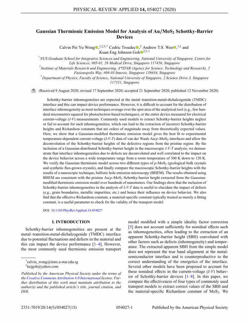
Figure 1 shows a schematic of the fabricated Au/MoS2Schottky diode and the corresponding scanning electronmicroscope (SEM) image. We use the bulk MoS2 crystalas the device material to allow clean shadow-mask fabri-cation and the metal-semiconductor interface formed withthe top layer can provide the basic understanding of metalcontacts to layered semiconductor devices. Ti is chosenas the Ohmic contact as it is a commonly used materialfor Ohmic contacts to MoS2. We choose Au as the Schot-tky contact as it is a high-work-function metal that is not
(a)
(b)
FIG. 1. (a) Schematic of the Au/MoS2 device. Contacts A andB are used to perform I-V measurements and the scanning tun-neling microscope (STM) tip is added for BHEM measurements,(b) the corresponding scanning electron micrograph showingactual device during BHEM measurements. Imaging conditions:0.1-kV acceleration voltage, 20-pA current.
expected to form Ohmic contacts with MoS2 without inter-face modification, and it is also a commonly used contactmaterial in the literature due to its inertness in the ambientenvironment.
III. EXPERIMENT
The p-type geological bulk MoS2 crystal is obtainedfrom Ward’s Science [32], the p-type synthetic flux-grownMoS2 crystal (intrinsic) is obtained from 2D semiconduc-tors [33]. The Ohmic contacts to the MoS2 crystals aredeposited in a high vacuum e-beam evaporator system(AJA International) after cleaving off the top surface usingsticky tape to obtain a fresh surface for the evaporation ofTi(5 nm)/Au(80 nm) at a base pressure of 1 × 10⁻⁸ mbarto form Ohmic contacts. After deposition of the Ohmiccontacts, the MoS2 is transferred ex situ to a thermal evap-orator system equipped with an annealing stage (R-DEC)for the Schottky-contact deposition. First, the MoS2 crys-tal is annealed at 350 °C for 2.5 h to improve the quality ofthe Ohmic contacts by removing physisorbed material atthe interface or to promote an interface reaction of Ti withthe MoS2 surface, and to outgas physisorbed contaminantson the surface of the MoS2 crystal. Next, Au(15 nm) is
054027-4
GAUSSIAN THERMIONIC EMISSION MODEL . . . PHYS. REV. APPLIED 14, 054027 (2020)
thermally evaporated onto the clean surface of the MoS2crystal through a shadow mask at the rate of 0.2 Å/s atapproximately 50 °C at a base pressure of 1 × 10⁻⁸ mbar.The larger circular Au devices are 500 µm in diameterand the smaller circular Au devices are 250 µm in diam-eter, while the rectangular Ti/Au Ohmic contacts on eachside of the substrate are 0.7 × 7 mm2
. Finally, the sam-ples are transferred ex situ to an UHV Nanoprobe system(Omicron), which is an ultrahigh-vacuum (base pressure1 × 10−10 mbar) four-probe STM system equipped withthree standard STM probes for contacted I-V measure-ments, one atomic resolution capable STM probe and aZeiss Gemini SEM imaging column for accurate position-ing of the probes. The devices are measured without furtherannealing to prevent modification of the as-deposited inter-face. The manifestation of epitaxial Au(111) steps in theovergrowth Au cap layer (Fig. 6) provides an indication ofgood interface cleanliness and quality of this preparationmethod.
IV. RESULTS
A. I-V-T measurements
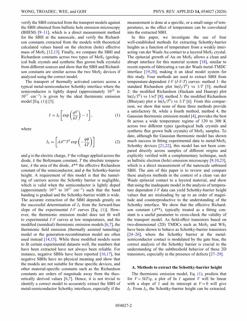
Figure 2 shows the I-V-T measurements of Au/geological MoS2 and the Au/synthetic MoS2 Schottkydiodes. From the I-V-T characteristics of the devices, weobserve the typical rectifying behavior of a p-type Schot-tky diode with low leakage at positive bias and currentturn on at negative biases and hence can conclude thatour MoS2 devices are p type. A shunt conduction path-way, which could arise from conduction through defectiveregions with lower resistance is present for the geologicalMoS2 crystal. The synthetic MoS2 device shows a typi-cal diode I-V characteristic with low leakage under reversebias, turn on at threshold followed by monatomic rise in I,with no defect-dominated shunt at low biases, from whichwe can conclude that the synthetic MoS2 crystal is cleaner.The presence of a high series resistance complicates theanalysis due to voltage drop across the series resistance,
(a) (b)
(c) (d)
FIG. 2. (a) Temperature-dependent current-voltage (I-V-T) measurements of Au/geological p-MoS2 from 300 K (room temperature)to 120 K. The device area is 0.196 mm2. (b) Plots of extracted diode parameters for the Au/geological MoS2 Schottky diode againsttemperature. Ideality factor (red, left axis) and barrier height (blue, right axis). (c) Temperature-dependent current-voltage (I-V-T)measurements of Au/synthetic p-MoS2 and (d) the extracted diode parameters for the Au/synthetic MoS2 devices. Black lines areguides to the eye for showing two ideality-factor ranges. The error bars of n ± 0.05 and φ ± 0.02 eV are estimated from the error ofrange of fit of Eq. (3) to Figs. 2(a) and 2(c).
054027-5
WONG, TROADEC, WEE, and GOH PHYS. REV. APPLIED 14, 054027 (2020)
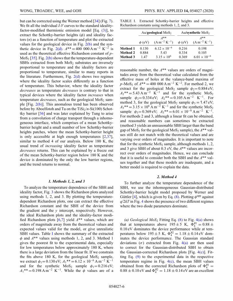
but can be corrected using the Werner method [34] (Fig. 7).We fit all the individual I-V curves to the standard ideality-factor-modified thermionic emission model [Eq. (3)], toextract the Schottky-barrier heights (φ) and ideality fac-tors (n) as a function of temperature and plot the extractedvalues for the geological device in Fig. 2(b) and the syn-thetic device in Fig. 2(d). A** = 400 000 A m−2 K−2 isused as the theoretical effective Richardson constant of p-MoS2 [35]. Fig. 2(b) shows that the temperature-dependentSBHs extracted from both MoS2 substrates are inverselyproportional to temperature and the ideality factors areproportional to temperature, similar to many reports inthe literature. Furthermore, Fig. 2(d) shows two regimeswhere the ideality factor scales differently as a functionof temperature. This behavior, where the ideality factordecreases as temperature decreases is contrary to that intypical devices where the ideality factor increases whentemperature decreases, such as the geological MoS2 sam-ple [Fig. 2(b)]. This anomalous trend has been observedbefore by Aboelfotoh and Tu on the TiSi2/n-Si(100) Schot-tky barrier [36] and was later explained by Tung to arisefrom a convolution of charge transport through a inhomo-geneous interface, which comprises of a mean Schottky-barrier height and a small number of low Schottky-barrierheights patches, where the mean Schottky-barrier heightis only accessible at high enough temperatures [2,37],similar to method 4 of our analysis. Below 180 K, theusual trend of increasing ideality factor as temperaturedecreases returns. This can be explained by a freeze outof the mean Schottky-barrier region below 180 K and thedevice is dominated by the only the low barrier regions,and the trend returns to normal.
1. Methods 1, 2, and 3
To analyze the temperature dependence of the SBH andideality factor, Fig. 3 shows the Richardson plots analyzedusing methods 1, 2, and 3. By plotting the temperature-dependent Richardson plots, one can extract the effectiveRichardson constant and the SBH of the device fromthe gradient and the y intercept, respectively. However,the ideal Richardson plots and the ideality-factor modi-fied Richardson plots [6,7] yield A** values, which areorders of magnitude away from the theoretical values andexpected values valid for the model, or give unrealisticSBH values. Table I shows the summary of the extractedφ and A** values using methods 1, 2, and 3. Method 1gives the poorest fit to the experimental data, especiallyfor low temperatures below approximately 180 K, wherethere is a large deviation from the linear fit. If we constrainthe fits above 180 K, for the geological MoS2 sample,we extract φ1= 0.130 eV; A1** = 6.12 × 10⁻⁶ A m−2 K−1
and for the synthetic MoS2 sample φ1= 0.216 eV;A1** = 0.198 A m−2 K−1. While the φ values are of a
TABLE I. Extracted Schottky-barrier heights and effectiveRichardson constants using methods 1, 2, and 3.
Au/geological MoS2 Au/synthetic MoS2
φ (eV)A**
(A m−2 K−1) φ (eV)A**
(A m−2 K−1)
Method 1 0.130 6.12 × 10⁻⁶ 0.216 0.198Method 2 0.884 5.43 0.334 0.105Method 3 1.47 3.15 × 10⁶ 0.369 6.01 × 10⁻⁶
reasonable number, the A** values are orders of magni-tudes away from the theoretical value calculated from theeffective mass of holes at the valance-band maxima ofp-MoS2 of A** = 400 000 A m−2 K−2. For method 2, weextract for the geological MoS2 sample φ2= 0.884 eV;A2** = 5.43 A m−2 K−1 and for the synthetic MoS2sample φ2= 0.334 eV; A2** = 0.105 A m−2 K−1. Formethod 3, for the geological MoS2 sample φ3 = 1.47 eV;A3** = 3.15 × 10⁶ A m−2 K−1 and for the synthetic MoS2sample φ3= 0.369 eV; A3** = 6.01 × 10⁻⁶ A m−2 K−1.For methods 2 and 3, although a linear fit can be obtained,and reasonable numbers can sometimes be extracted(method 3 yields an unreasonable SBH larger than the bandgap of MoS2 for the geological MoS2 sample), the A** val-ues still do not match with the theoretical values and arevarying over orders of magnitudes. It is important to notethat for the synthetic MoS2 sample, although methods 1, 2,and 3 give SBH of about 0.3 eV, the A** values are incor-rect over orders of magnitudes. Hence, we can concludethat it is useful to consider both the SBH and the A** val-ues together and that these models are inadequate, and abetter model is required to explain the data.
2. Method 4
To further analyze the temperature dependence of theSBH, we use the inhomogeneous Gaussian-distributedSchottky-barrier height model proposed by Werner andGüttler [4], which is given by Eq. (8). Plotting φapp againstq/2kT in Fig. 4 shows the presence of two different regimeswhere the two diode parameters dominate.
(a) Geological MoS2 Fitting Eq. (8) to Fig. 4(a) showsthat at temperatures above 195 ± 5 K, �B1
4 = 0.88 ±0.10 eV dominates the device performance while at tem-peratures below 195 ± 5 K, �B2
4 = 1.18 ± 0.14 eV dom-inates the device performance. The Gaussian standarddeviations (σ ) extracted from Fig. 4(a) are then usedto correct for the Gaussian-distributed SBH to obtainthe Gaussian-corrected Richardson plots [Fig. 4(c)]. Fit-ting Eq. (9) to the experimental data in the respectivetemperature regime in Fig. 4(c), the mean SBH valuesobtained from the corrected Richardson plots of �B1
4 =0.88 ± 0.10 eV and �B2
4 = 1.18 ± 0.14 eV are an excellent
054027-6

GAUSSIAN THERMIONIC EMISSION MODEL . . . PHYS. REV. APPLIED 14, 054027 (2020)
(a)
(b)
(c)
In(I S
/T2 )
In(I S
/T2 )
In(I S
/T2 )
In(I S
/T2 )
n In
(I S/T
2 )
n In
(I S/T
2 )
FIG. 3. Richardson plots and their ideality-factor-modified Richardson plots variants for the Au/geological MoS2 (left column) andthe Au/synthetic MoS2 (right column). (a) Method 1: standard Richardson plot ln (IS/T2) against 1/T. (b) Method 2: modified ln (IS/T2)against 1/nT and (c) Method 3: modified n ln (IS/T2) against 1/T. Error bars are estimated with φ ± 0.02 eV and n ± 0.05 from fittingerrors to extract SBH and n.
054027-7

WONG, TROADEC, WEE, and GOH PHYS. REV. APPLIED 14, 054027 (2020)
(a) (b)
(c) (d)
FIG. 4. (a) Double Gaussian plot of φapp± against q/2kT for the Au/geological MoS2 crystal and (b) the Au/synthetic MoS2 crystal.The solid lines are linear fits to Eq. (8) to obtain the mean Schottky-barrier height � and the standard deviation σ of the Gaussiandistribution. (c) Modified Richardson plot for the Au/geological MoS2 crystal and (d) Au/synthetic MoS2 crystal. The two plots arecorrected with the σ of the Gaussian distributions in their respective temperature regimes. Linear fits to Eq. (9) give the �4 from thegradient of the fit and A4** from the intercept.
match with the values obtained in Fig. 4(a), �B14 = 0.88 ±
0.10 eV and �B24 = 1.17 ± 0.14 eV. The average Richard-
son constants extracted from the Gaussian-correctedRichardson plot of A4** = 406 000 ± 145 000 A m−2 K−1
is in good agreement with theoretical quantum-correctedvalue of A** = 400 000 A m−2 K−1 [12,13], validating thefeasibility of this method.
(b) Synthetic flux grown MoS2 Similarly for the syn-thetic MoS2 crystal, Fig. 4(b) shows that at high tem-peratures above 195 ± 5 K, the �B1
4 = 0.86 ± 0.12 eVdominates the device performance while at low temper-atures, the �B2
4 = 0.65 ± 0.08 eV dominates the deviceperformance. Plotting the Gaussian-modified Richardsonplot in Fig. 4(d) reveals a similar behavior as the geo-logical MoS2 sample. The mean SBH values extractedfrom the Richardson plots of �B1
4 = 0.84 ± 0.12 eV and�B2
4 = 0.65 ± 0.08 eV are an excellent match with the
values obtained in Fig. 4(b) with a similar temperaturecrossover range of 195 ± 5 K. Furthermore, the averageA4** extracted from the synthetic MoS2 of 424 000 ± 23000 A m−2 K−1 is in excellent agreement with the A4**of geological MoS2 of 406 000 ± 145 000 A m−2 K−1,and again with the theoretically derived values of 400000 A m−2 K−2. These results provide crucial support forthe validity of using the Gaussian-modified SBH model inour samples.
B. BHEM
To further verify the presence of a Gaussian-distributedSBH, we use ballistic hole emission microscopy (BHEM),which is a nanoscale technique based on scanning tunnel-ing microscopy (STM) to measure the local SBH of theinterface for the two different MoS2 crystals. In a typicalBHEM experiment, holes are injected into the Au layerfrom the STM tip by applying a positive tip bias (VT),while the Au layer and the MoS2 substrate are grounded
054027-8

GAUSSIAN THERMIONIC EMISSION MODEL . . . PHYS. REV. APPLIED 14, 054027 (2020)
[Fig. 1(a)]. Some of the holes travel through the thin Aulayer (15 nm) unscattered (the ballistic holes) to reachthe metal-semiconductor interface and are collected as theBHEM current (IB) at the Ti/Au Ohmic contact if theyhave enough energy to overcome the Schottky barrier andfulfil the momentum conservation rules [9,38]. To obtainthe local Schottky-barrier height (φBHEM), we use the spec-troscopy mode by holding the STM tip at a fixed (x, y)position with the tunnelling current (IT) feedback loop kepton, and collect the BHEM current (IB) as a function of thebias (VT) applied between the tip and the Au layer. Wenormalize the transmission (R) of the interface by takingthe ratio of the IB and the IT and plotted this ratio againstthe tip bias to obtain the BHEM spectra [Eq. (10)], whichis a function of the transmission of the interface to theenergy of the electrons. In addition to the main advantageof the nanoscale spatial resolution in BHEM, the zero biasSBH (i.e., the equilibrium band alignment) can be mea-sured and visualized directly without having to assume atransport model. For one dataset, we collect approximately800 BHEM spectra over a 200 nm by 200 nm area andextract the local SBH by fitting an individual spectrum tothe Prietsch-Ludeke (PL) model [Eq. (10)] in the range of0.3 to 1.3 V, about 0.4 V above the SBH [38,39] (Fig. 8).A statistical R2 value is used to select the quality of fit ofthe spectra, for R2 < 0.6, the spectra are rejected. Usually,these rejected spectra have either no threshold, or displaysudden current jumps due to equipment instability.
IB
IT= R
(φBHEM − eV)
eV
5/2
. (10)
We collected a few datasets over a few different locationson the same sample and Fig. 5 shows a representative sta-tistical spread of the local SBH for the two crystals takenfrom one of the datasets. For the Au/geological MoS2device, we obtain the local φBHEM = 0.86 ± 0.02 eV,while for the Au/synthetic MoS2, we obtain a φBHEM =0.89 ± 0.02 eV. The nanoscale SBH for both the geolog-ical and synthetic Au/MoS2 samples are similar, affirmingthat although the crystal quality is likely to be different, thepristine SBH is similar in value and a Gaussian distributionwith σ = 0.02 eV is present for both samples.
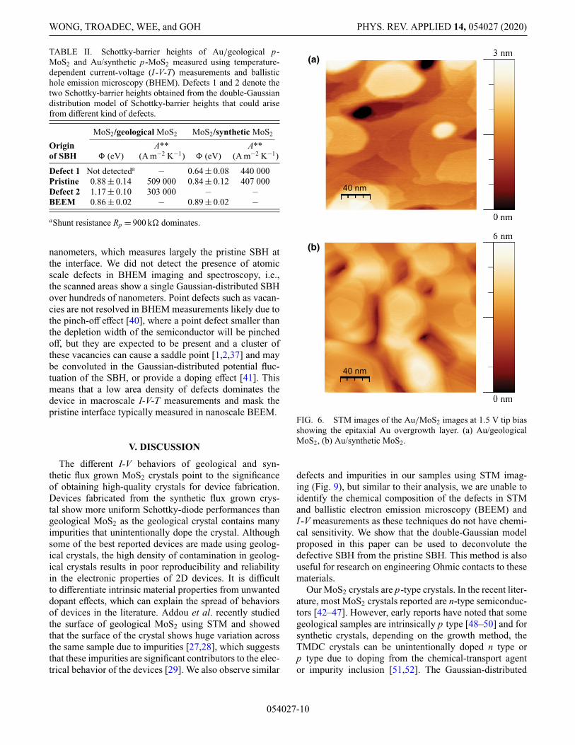
Table II shows the summary of the Schottky-barrierheights obtained for the Au/geological p-MoS2 andAu/synthetic p-MoS2 using I-V-T measurements andBHEM. We propose that the pristine zero-bias SBH forthe Au/p-MoS2 interface is approximately 0.86 eV as thisvalue is obtained across complementary techniques anddifferent MoS2 sources. There is at least one defectiveregion present in each sample. We generalize these defectsinto two regimes, defect 1 is a lower-barrier region, whichis present in both the geological and synthetic MoS2 crys-tals. The density of defect 1 in the geological crystal couldbe higher, and thus exists as a shunt region. We propose
(a)
(b)
FIG. 5. Statistical plot of the Schottky-barrier height mea-sured at 120 K for (a) Au(15 nm) /geological MoS2, φBHEM =0.86 ± 0.02 eV, 770 data points. (b) Au(15 nm)/synthetic MoS2,φBHEM = 0.89 ± 0.02, 797 data points.
that the convolution of the lower-barrier defect with thepristine SBH can explain the spread of SBH values in theliterature as the extracted numbers will differ across dif-ferent samples and measurement temperatures. Defect 2 isassociated with the higher-barrier region possibly by dop-ing, only detected in the geological MoS2 crystal, typicallynot a dominating effect in the I-V measurements due tothe exponential relationship of I to φ in the thermionicemission model.
From Table II, we can conclude that the nanoscale SBHmeasured using BHEM and macroscale SBH determinedusing I-V-T measurements are in excellent agreement.Standard deviations of the macroscale SBH are one orderof magnitude larger than the nanoscale SBH. This can beexplained by the nonuniform area of the measurement. I-V-T measurements give a weighted average of the SBHacross the whole device area (0.196 mm2), which includescontributions from defects such as step edges, impurities,etc. while the nanoscale SBH has a resolution of a few
054027-9
WONG, TROADEC, WEE, and GOH PHYS. REV. APPLIED 14, 054027 (2020)
TABLE II. Schottky-barrier heights of Au/geological p-MoS2 and Au/synthetic p-MoS2 measured using temperature-dependent current-voltage (I -V-T) measurements and ballistichole emission microscopy (BHEM). Defects 1 and 2 denote thetwo Schottky-barrier heights obtained from the double-Gaussiandistribution model of Schottky-barrier heights that could arisefrom different kind of defects.
MoS2/geological MoS2 MoS2/synthetic MoS2
Originof SBH � (eV)
A**(A m−2 K−1) � (eV)
A**(A m−2 K−1)
Defect 1 Not detecteda – 0.64 ± 0.08 440 000Pristine 0.88 ± 0.14 509 000 0.84 ± 0.12 407 000Defect 2 1.17 ± 0.10 303 000 – –BEEM 0.86 ± 0.02 – 0.89 ± 0.02 –
aShunt resistance Rp = 900 k� dominates.
nanometers, which measures largely the pristine SBH atthe interface. We did not detect the presence of atomicscale defects in BHEM imaging and spectroscopy, i.e.,the scanned areas show a single Gaussian-distributed SBHover hundreds of nanometers. Point defects such as vacan-cies are not resolved in BHEM measurements likely due tothe pinch-off effect [40], where a point defect smaller thanthe depletion width of the semiconductor will be pinchedoff, but they are expected to be present and a cluster ofthese vacancies can cause a saddle point [1,2,37] and maybe convoluted in the Gaussian-distributed potential fluc-tuation of the SBH, or provide a doping effect [41]. Thismeans that a low area density of defects dominates thedevice in macroscale I-V-T measurements and mask thepristine interface typically measured in nanoscale BEEM.
V. DISCUSSION
The different I-V behaviors of geological and syn-thetic flux grown MoS2 crystals point to the significanceof obtaining high-quality crystals for device fabrication.Devices fabricated from the synthetic flux grown crys-tal show more uniform Schottky-diode performances thangeological MoS2 as the geological crystal contains manyimpurities that unintentionally dope the crystal. Althoughsome of the best reported devices are made using geolog-ical crystals, the high density of contamination in geolog-ical crystals results in poor reproducibility and reliabilityin the electronic properties of 2D devices. It is difficultto differentiate intrinsic material properties from unwanteddopant effects, which can explain the spread of behaviorsof devices in the literature. Addou et al. recently studiedthe surface of geological MoS2 using STM and showedthat the surface of the crystal shows huge variation acrossthe same sample due to impurities [27,28], which suggeststhat these impurities are significant contributors to the elec-trical behavior of the devices [29]. We also observe similar
40 nm
40 nm
(a)
(b)
FIG. 6. STM images of the Au/MoS2 images at 1.5 V tip biasshowing the epitaxial Au overgrowth layer. (a) Au/geologicalMoS2, (b) Au/synthetic MoS2.
defects and impurities in our samples using STM imag-ing (Fig. 9), but similar to their analysis, we are unable toidentify the chemical composition of the defects in STMand ballistic electron emission microscopy (BEEM) andI -V measurements as these techniques do not have chemi-cal sensitivity. We show that the double-Gaussian modelproposed in this paper can be used to deconvolute thedefective SBH from the pristine SBH. This method is alsouseful for research on engineering Ohmic contacts to thesematerials.
Our MoS2 crystals are p-type crystals. In the recent liter-ature, most MoS2 crystals reported are n-type semiconduc-tors [42–47]. However, early reports have noted that somegeological samples are intrinsically p type [48–50] and forsynthetic crystals, depending on the growth method, theTMDC crystals can be unintentionally doped n type orp type due to doping from the chemical-transport agentor impurity inclusion [51,52]. The Gaussian-distributed
054027-10
GAUSSIAN THERMIONIC EMISSION MODEL . . . PHYS. REV. APPLIED 14, 054027 (2020)
model should also work for n-type MoS2 and otherTMDCs. Cook et al. studied the n-type MoS2 using BEEMand they obtained the Au/n-MoS2 SBH of 0.48 ± 0.02 eVfor 16 nm Au layers [53]. Our p-type SBH and theirn-type SBH for approximately 15 nm Au layer sum upto approximately the band gap of bulk MoS2 (approx-imately 1.34 eV), which provides a useful consistencycheck, and suggests an unpinned Fermi level. We do notdetect any signature of strain in our devices at the limitof resolution of our Raman spectrograph (Fig. 10), sug-gesting that the strain did not play a significant role inour measurements. Figure 6 shows the STM image ofepitaxial Au films on MoS2 grown using a slow depo-sition method, which is an indirect evidence of a cleanabrupt interface Au/MoS2 [18,20]. Our results lend sup-port to the presence of an unpinned Fermi level for awell-prepared van der Waal’s Au/MoS2 interface that isdeposited slowly (approximately 0.2 Å/s), consistent witha few recent reports [19,20], and an old photoemissionstudy [54].
Our BHEM results seem to point to the presence of lowelastic scattering, as our SBH distribution can be well mod-eled by a single symmetric Gaussian distribution. This isconsistent with the results of Nolting et al., where a sin-gle symmetric Gaussian distribution can be well fit to awell-prepared abrupt metal-semiconductor interface with-out any interface reactions [55–57]. We also note thatthe Gaussian-distributed SBH analysis method we proposein this paper has been applied also to monolayer MoS2devices [58]. In their report, Moon et al. analyzed the topand edge contact of Au/MoS2 n-type FET devices usingthe Gaussian-distribution model at different gate bias. Theyobserve the top contact has a larger SBH and larger σ ,showing more inhomogeneity than in the edge contact,which has a lower SBH and lower σ . However, they didnot use the Gaussian-corrected Richardson plot, but theyindicated that the standard Richardson plot is not valid dueto an observed temperature dependence of the SBH. Ourmethod of analysis can be used to bridge the gap betweenreal 2D devices and theoretically proposed models [24] bydeconvoluting SBH inhomogeneity from intrinsic materialtransport behaviors.
VI. CONCLUSION
We show that the presence of inhomogeneities at themetal-semiconductor interface should be considered in theextraction of device parameters. The analysis of I-V-Tmeasurements without considering the Gaussian distri-bution of Schottky-barrier heights results in an apparentSchottky-barrier height (φapp), which is not reflecting theintrinsic behavior of the interface, but the convolutedeffects of low barrier regions (defects), pristine regions,and temperature. Using the Gaussian-modified Richardsonplots, reliable mean SBH (�) can be extracted, and the
extracted effective Richardson constants (A**) are close tothe theoretical calculated Richardson constants. We reportan experimentally measured value of A** = 415 000 ± 85000 A m−2 K−1 based on our averaged A** measurementsin contrast to A** = 745 000 A m−2 K−1 typically assumedfor p-type MoS2 devices and the Au/p- MoS2 SBH ofapproximately 0.86 ± 0.14 eV obtained as an averagedvalue across two different samples and complementarytechniques.
We used BHEM, which is a more tedious but directmethod to measure the zero-bias SBH without the need torely on the validity of temperature-dependent models, andto experimentally validate the significance of including aGaussian-distributed SBH at the nanoscale in conventionalI-V-T analysis. Our results provide the basic framework forextracting the pristine SBH from temperature-dependentI-V data and demonstrate that with careful use of thedual parameter (A** + SBH) analysis, we avoid obtainingunphysical numbers that are counterproductive for under-standing such interfaces. This implies that the I-V-T anal-ysis can yield useful insights on the SB inhomogeneitieseven though it might be a macroscale measurement.
ACKNOWLEDGMENTS
This research is supported by the Agency for Science,Technology and Research (A*STAR) under its A*STARQTE Grant No. A1685b0005 and the A*STAR PharosGrant No. 1527000016.
APPENDIX A: WERNER METHOD
The Werner method is used to correct for the high seriesresistance present in the I-V-T curves of our Au/MoS2diodes [34]. Under forward bias and with series-resistancecontribution, the voltage across the diode, VD = V−IRs andVD � kT, the thermionic emission current [Eq. (A1)] isgiven by the simplified form:
ID = IS exp[
q(V − IRs)
nkT
], (A1)
where ID is the thermionic diode current. DifferentiatingEq. (A1) gives the small signal conductance G = dID/dVand one obtains
GID
= qnkT
(1 − GRs). (A2)
Werner showed that by plotting G/ID against G, namedhereafter as the Werner plot, will give a straight line witha y-axis intercept of q/nkT, where n can be extracted, andthe x axis gives the intercept of 1/Rs.
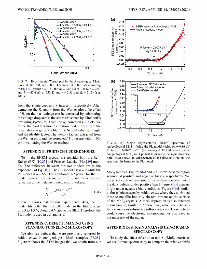
Figure 7 shows the representative experimental Wernerplot for our Au/MoS2 diode at 300, 250, and 200 K fromwhich their respective n and Rs values can be extracted
054027-11
WONG, TROADEC, WEE, and GOH PHYS. REV. APPLIED 14, 054027 (2020)
FIG. 7. Experimental Werner plot for the Au/geological MoS2diode at 300, 250, and 200 K. The linear fit to the data accordingto Eq. (A2) yields n = 1.73 and Rs = 28.4 k� at 300 K, n = 2.03and Rs = 42.6 k� at 250 K and n = 2.35 and Rs = 71.2 k� at200 K.
from the y intercept and x intercept, respectively. Afterextracting the Rs and n from the Werner plots, the effectof Rs on the bias voltage can be corrected by subtractingthe voltage drop across the series resistance by Kirchhoff’slaw using VD=V-IRs. From the Rs-corrected I-V plots, wefit the standard thermionic emission model [Eq. (3)] in thelinear diode regime to obtain the Schottky-barrier heightand the ideality factor. The ideality factors extracted fromthe Werner plots and the corrected I-V plots are within 10%error, validating the Werner method.
APPENDIX B: PRIETSCH-LUDEKE MODEL
To fit the BHEM spectra, we consider both the Bell-Kaiser (BK) [10,23] and Prietsch-Ludeke (PL) [39] mod-els. The difference between the two models are in theexponent n of Eq. (B1). The BK model has n = 2 while thePL model is n = 5/2. The additional 1/2 power for the PLmodel comes from the inclusion of quantum-mechanicalreflection at the metal-semiconductor interface.
IB
IT= R
(φB − eV)
eV
n
. (B1)
Figure 8 shows that for our experimental data, the PLmodel fits better than the BK model in the fitting rangeof 0.3 to 1.3 V, about 0.4 V above the SBH. Therefore, thePL model is used in our analysis.
APPENDIX C: DEFECT IMAGING USINGSCANNING TUNNELING MICROSCOPY
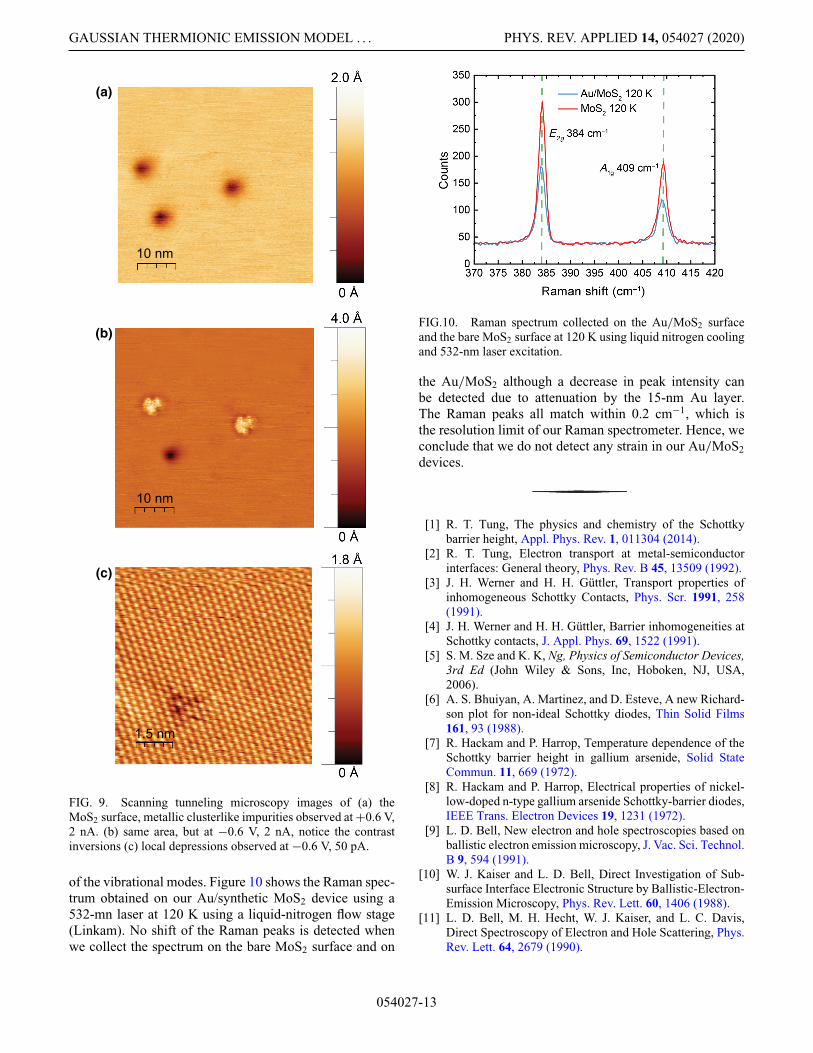
We also see defects that were previously reported byAddou et al. in our geological MoS2 samples [27,28].Figure 9 shows the STM images that we obtain from our
BEEM spectra-Au/geological MoS2
Averaged BEEM spectra
Bell-Kaiser model
BE
EM
tran
smis
sion
(%
)(I
BE
EM
/I Tun
nel ×
100
%)
BE
EM
tran
smis
sion
(%
)(I
BE
EM
/I Tun
nel ×
100
%)
Prietsch-Ludeke model
Prietsch-Ludeke model
Tip bias (eV)
Tip bias (eV)
R factor = 0.0077 eV–1
fB = 0.86 eV
(a)
(b)
FIG. 8. (a) Single representative BEEM spectrum ofAu/geological MoS2, fitting the PL model yields φB = 0.86 eVR factor = 0.0077 eV−1 (b) Averaged BEEM spectrum ofAu/geological MoS2 (674 points) to increase the signal-to-noiseratio. Inset shows an enlargement of the threshold region, thespectrum fits better to the PL model.
MoS2 samples. Figures 9(a) and 9(b) show the same regionscanned at positive and negative biases, respectively. Weobserve a contrast inversion of some defects where two ofthe dark defects under positive bias [Figure 9(a)] appearsbright under negative-bias conditions [Figure 9(b)] similarto those defects seen by Addou et al., where they attributedthese to metallic impurity clusters present on the surfaceof the MoS2 crystals. A local depression is also detectedin our sample, similar to Addou at al., which could be sul-fur vacancies or subsurface sulfur vacancies. These defectscould cause the electronic inhomogeneities discussed inthe main text of the paper.
APPENDIX D: STRAIN ANALYSIS USING RAMANSPECTROSCOPY
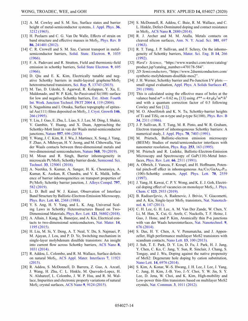
To study the effect of strain at our Au/MoS2 interface,we use Raman spectroscopy to compare the relative shifts
054027-12
GAUSSIAN THERMIONIC EMISSION MODEL . . . PHYS. REV. APPLIED 14, 054027 (2020)
10 nm
10 nm
1.5 nm
(a)
(b)
(c)
FIG. 9. Scanning tunneling microscopy images of (a) theMoS2 surface, metallic clusterlike impurities observed at +0.6 V,2 nA. (b) same area, but at −0.6 V, 2 nA, notice the contrastinversions (c) local depressions observed at −0.6 V, 50 pA.
of the vibrational modes. Figure 10 shows the Raman spec-trum obtained on our Au/synthetic MoS2 device using a532-mn laser at 120 K using a liquid-nitrogen flow stage(Linkam). No shift of the Raman peaks is detected whenwe collect the spectrum on the bare MoS2 surface and on
FIG.10. Raman spectrum collected on the Au/MoS2 surfaceand the bare MoS2 surface at 120 K using liquid nitrogen coolingand 532-nm laser excitation.
the Au/MoS2 although a decrease in peak intensity canbe detected due to attenuation by the 15-nm Au layer.The Raman peaks all match within 0.2 cm−1, which isthe resolution limit of our Raman spectrometer. Hence, weconclude that we do not detect any strain in our Au/MoS2devices.
[1] R. T. Tung, The physics and chemistry of the Schottkybarrier height, Appl. Phys. Rev. 1, 011304 (2014).
[2] R. T. Tung, Electron transport at metal-semiconductorinterfaces: General theory, Phys. Rev. B 45, 13509 (1992).
[3] J. H. Werner and H. H. Güttler, Transport properties ofinhomogeneous Schottky Contacts, Phys. Scr. 1991, 258(1991).
[4] J. H. Werner and H. H. Güttler, Barrier inhomogeneities atSchottky contacts, J. Appl. Phys. 69, 1522 (1991).
[5] S. M. Sze and K. K, Ng, Physics of Semiconductor Devices,3rd Ed (John Wiley & Sons, Inc, Hoboken, NJ, USA,2006).
[6] A. S. Bhuiyan, A. Martinez, and D. Esteve, A new Richard-son plot for non-ideal Schottky diodes, Thin Solid Films161, 93 (1988).
[7] R. Hackam and P. Harrop, Temperature dependence of theSchottky barrier height in gallium arsenide, Solid StateCommun. 11, 669 (1972).
[8] R. Hackam and P. Harrop, Electrical properties of nickel-low-doped n-type gallium arsenide Schottky-barrier diodes,IEEE Trans. Electron Devices 19, 1231 (1972).
[9] L. D. Bell, New electron and hole spectroscopies based onballistic electron emission microscopy, J. Vac. Sci. Technol.B 9, 594 (1991).
[10] W. J. Kaiser and L. D. Bell, Direct Investigation of Sub-surface Interface Electronic Structure by Ballistic-Electron-Emission Microscopy, Phys. Rev. Lett. 60, 1406 (1988).
[11] L. D. Bell, M. H. Hecht, W. J. Kaiser, and L. C. Davis,Direct Spectroscopy of Electron and Hole Scattering, Phys.Rev. Lett. 64, 2679 (1990).
054027-13
WONG, TROADEC, WEE, and GOH PHYS. REV. APPLIED 14, 054027 (2020)
[12] A. M. Cowley and S. M. Sze, Surface states and barrierheight of metal-semiconductor systems, J. Appl. Phys. 36,3212 (1965).
[13] H. Peelaers and C. G. Van De Walle, Effects of strain onband structure and effective masses in MoS2, Phys. Rev. B86, 241401 (2012).
[14] C. R. Crowell and S. M. Sze, Current transport in metal-semiconductor barriers, Solid. State. Electron. 9, 1035(1966).
[15] F. A. Padovani and R. Stratton, Field and thermionic-fieldemission in schottky barriers, Solid State Electron. 9, 695(1966).
[16] D. Qiu and E. K. Kim, Electrically tunable and neg-ative Schottky barriers in multi-layered graphene/MoS2heterostructured transistors, Sci. Rep. 5, 13743 (2015).
[17] M. Tao, D. Udeshi, S. Agarwal, R. Kolappan, Y. Xu, E.Maldonado, and W. P. Kirk, Se-Passivated Si(100) surfacefor low and negative Schottky barriers, Ext. Abstr. FourthInt. Work. Junction Technol. IWJT 2004 4, 119 (2004).
[18] S. Nagashima and I. Otsuka, Surface topography of epitax-ial Au(111) films deposited on MoS2, J. Cryst. Growth 146,266 (1995).
[19] Y. Liu, J. Guo, E. Zhu, L. Liao, S. J. Lee, M. Ding, I. Shakir,V. Gambin, Y. Huang, and X. Duan, Approaching theSchottky-Mott limit in van der Waals metal-semiconductorjunctions, Nature 557, 696 (2018).
[20] Y. Wang, J. C. Kim, R. J. Wu, J. Martinez, X. Song, J. Yang,F. Zhao, A. Mkhoyan, H. Y. Jeong, and M. Chhowalla, Vander Waals contacts between three-dimensional metals andtwo-dimensional semiconductors, Nature 568, 70 (2019).
[21] M. Moun and R. Singh, Barrier inhomogeneity inmicroscale Pt/MoS2 Schottky barrier diode, Semicond. Sci.Technol. 33, 125001 (2018).
[22] A. Neetika, S. Kumar, A. Sanger, H. K. Chourasiya, A.Kumar, K. Asokan, R. Chandra, and V. K. Malik, Influ-ence of barrier inhomogeneities on transport properties ofPt/MoS2 Schottky barrier junction, J. Alloys Compd. 797,582 (2019).
[23] L. D. Bell and W. J. Kaiser, Observation of InterfaceBand Structure by Ballistic-Electron-Emission Microscopy,Phys. Rev. Lett. 61, 2368 (1988).
[24] Y. S. Ang, H. Y. Yang, and L. K. Ang, Universal Scal-ing Laws in Schottky Heterostructures Based on Two-Dimensional Materials, Phys. Rev. Lett. 121, 56802 (2018).
[25] A. Allain, J. Kang, K. Banerjee, and A. Kis, Electrical con-tacts to two-dimensional semiconductors, Nat. Mater. 14,1195 (2015).
[26] H. Liu, M. Si, Y. Deng, A. T. Neal, Y. Du, S. Najmaei, P.M. Ajayan, J. Lou, and P. D. Ye, Switching mechanism insingle-layer molybdenum disulfide transistors: An insightinto current flow across Schottky barriers, ACS Nano 8,1031 (2014).
[27] R. Addou, L. Colombo, and R. M. Wallace, Surface defectson natural MoS2, ACS Appl. Mater. Interfaces 7, 11921(2015).
[28] R. Addou, S. McDonnell, D. Barrera, Z. Guo, A. Azcatl,J. Wang, H. Zhu, C. L. Hinkle, M. Quevedo-Lopez, H.N. Alshareef, L. Colombo, J. W. P. Hsu, and R. M. Wal-lace, Impurities and electronic property variations of naturalMoS2 crystal surfaces, ACS Nano 9, 9124 (2015).
[29] S. McDonnell, R. Addou, C. Buie, R. M. Wallace, and C.L. Hinkle, Defect-Dominated doping and contact resistancein MoS2, ACS Nano 8, 2880 (2014).
[30] R. J. Archer and M. M. Atalla, Metals contacts oncleaved silicon surfaces, Ann. N. Y. Acad. Sci. 101, 697(1963).
[31] R. T. Tung, J. P. Sullivan, and F. Schrey, On the inhomo-geneity of Schottky barriers, Mater. Sci. Eng. B 14, 266(1992).
[32] Ward’s Science, “https://www.wardsci.com/store/catalog/product.jsp?catalog_number=470178-584”.
[33] 2D Semiconductors, “https://www.2dsemiconductors.com/synthetic-molybdenum-disulfide-mos2”.
[34] J. H. Werner, Schottky barrier and Pn-Junction I/V plots —small signal evaluation, Appl. Phys. A Solids Surfaces 47,291 (1988).
[35] This is calculated using the effective mass of holes at thevalance band m* = 0.62 m0 [13] using A** = 4πqkB
2m*/h3
and with a quantum correction factor of 0.5 followingCowley and Sze [12].
[36] M. O. Aboelfotoh and K. N. Tu, Schottky-barrier heightsof Ti and TiSi2 on n-type and p-type Si(100), Phys. Rev. B34, 2311 (1986).
[37] J. P. Sullivan, R. T. Tung, M. R. Pinto, and W. R. Graham,Electron transport of inhomogeneous Schottky barriers: Anumerical study, J. Appl. Phys. 70, 7403 (1991).
[38] M. Prietsch, Ballistic-electron emission microscopy(BEEM): Studies of metal/semiconductor interfaces withnanometer resolution, Phys. Rep. 253, 163 (1995).
[39] M. Prietsch and R. Ludeke, Ballistic-Electron-EmissionMicroscopy and Spectroscopy of GaP(110)-Metal Inter-faces, Phys. Rev. Lett. 66, 2511 (1991).
[40] A. Olbrich, J. Vancea, F. Kreupl, and H. Hoffmann, Poten-tial pinch-off effect in inhomogeneous Au/Co/GaAs67P33(100)-Schottky contacts, Appl. Phys. Lett. 70, 2559(1997).
[41] J. Yang, H. Kawai, C. P. Y. Wong, and K. E. J. Goh, Electri-cal doping effect of vacancies on monolayer MoS2, J. Phys.Chem. C 123, 2933 (2019).
[42] B. Radisavljevic, A. Radenovic, J. Brivio, V. Giacometti,and A. Kis, Single-layer MoS2 transistors, Nat. Nanotech-nol. 6, 147 (2011).
[43] C. H. Lee, G. H. Lee, A. M. Van Der Zande, W. Chen, Y.Li, M. Han, X. Cui, G. Arefe, C. Nuckolls, T. F. Heinz, J.Guo, J. Hone, and P. Kim, Atomically thin P-n junctionswith van der Waals heterointerfaces, Nat. Nanotechnol. 9,676 (2014).
[44] S. Das, H. Y. Chen, A. V. Penumatcha, and J. Appen-zeller, High performance multilayer MoS2 transistors withscandium contacts, Nano Lett. 13, 100 (2013).
[45] J. Suh, T. E. Park, D. Y. Lin, D. Fu, J. Park, H. J. Jung,Y. Chen, C. Ko, C. Jang, Y. Sun, R. Sinclair, J. Chang, S.Tongay, and J. Wu, Doping against the native propensityof MoS2: Degenerate hole doping by cation substitution,Nano Lett. 14, 6976 (2014).
[46] S. Kim, A. Konar, W.-S. Hwang, J. H. Lee, J. Lee, J. Yang,C. Jung, H. Kim, J.-B. Yoo, J.-Y. Choi, Y. W. Jin, S. Y.Lee, D. Jena, W. Choi, and K. Kim, High-mobility andLow-power thin-film transistors based on multilayer MoS2crystals, Nat. Commun. 3, 1011 (2012).
054027-14
GAUSSIAN THERMIONIC EMISSION MODEL . . . PHYS. REV. APPLIED 14, 054027 (2020)
[47] B. Radisavljevic, M. B. Whitwick, and A. Kis, Integratedcircuits and logic operations based on single-layer MoS2,ACS Nano 5, 9934 (2011).
[48] R. Mansfield and S. A. Salam, Electrical properties ofmolybdenite, Proc. Phys. Soc. Sect. B 66, 377 (1953).
[49] J. A. Wilson and A. D. Yoffe, The transition metal dichalco-genides discussion and interpretation of the observed opti-cal, electrical and structural properties, Adv. Phys. 18, 193(1969).
[50] A. Stesmans, S. Iacovo, and V. V. Afanas’Ev, ESR study ofP-type natural 2H-polytype MoS2 crystals: The As acceptoractivity, Appl. Phys. Lett. 109, 172104 (2016).
[51] A. Pisoni, J. Jacimovic, O. S. Barišic, A. Walter, B. Náfrádi,P. Bugnon, A. Magrez, H. Berger, Z. Revay, and L. Forrö,The role of transport agents in MoS2 single crystals, J. Phys.Chem. C 119, 3918 (2015).
[52] B. Schoenaers, A. Stesmans, and V. V. Afanas’Ev, ESRidentification of the nitrogen acceptor in 2H-polytype syn-thetic MoS2: Dopant level and activation, AIP Adv. 7,105006 (2017).
[53] M. Cook, R. Palandech, K. Doore, Z. Ye, G. Ye, R. He, andA. J. Stollenwerk, Influence of interface coupling on theelectronic properties of the Au/MoS2 junction, Phys. Rev.B 92, 201302 (2015).
[54] J. R. Lince, D. J. Carré, and P. D. Fleischauer, Schottky-barrier formation on a covalent semiconductor withoutFermi-level pinning: The metal-MoS2(0001) interface,Phys. Rev. B 36, 1647 (1987).
[55] W. Nolting, C. Durcan, A. J. Narasimham, and V. P.LaBella, Nanoscale Schottky barrier mapping of thermallyevaporated and sputter deposited W/Si(001) diodes usingballistic electron emission microscopy, J. Vac. Sci. Tech-nol., B 34, 04J110 (2016).
[56] W. Nolting, C. Durcan, and V. P. LaBella, Detec-tion of silicide formation in nanoscale visualization ofinterface electrostatics, Appl. Phys. Lett. 110, 141606(2017).
[57] W. Nolting, C. Durcan, S. Gassner, J. Goldberg, R. Bal-sano, and V. P. Labella, Nanoscale schottky barrier visu-alization utilizing computational modeling and ballisticelectron emission microscopy, J. Appl. Phys. 123, 245302(2018).
[58] B. H. Moon, G. H. Han, H. Kim, H. Choi, J. J. Bae, J.Kim, Y. Jin, H. Y. Jeong, M. K. Joo, Y. H. Lee, and S. C.Lim, Junction-structure-dependent Schottky barrier inho-mogeneity and device ideality of monolayer MoS2 Field-effect transistors, ACS Appl. Mater. Interfaces 9, 11240(2017).
054027-15