2001 heterostructure integrated thermionic cooling of
TRANSCRIPT

UNIVERSITY OF CALIFORNIA
Santa Barbara
Heterostructure Integrated ThermionicCooling of Optoelectronic Devices
by
Christopher LaBounty
Ph.D. Dissertation
ECE Technical Report # 01-09
Department of Electrical and Computer EngineeringUniversity of California, Santa Barbara, CA 93106

UNIVERSITY OF CALIFORNIA
Santa Barbara
Heterostructure Integrated Thermionic Cooling of Optoelectronic Devices
A dissertation submitted in partial satisfaction of the
requirements for the degree of
Doctor of Philosophy
in
Electrical Engineering
by
Christopher John LaBounty
Committee in charge:
Professor John E. Bowers, Chair
Professor Ali Shakouri, Co-Chair
Professor Umesh Mishra
Professor Evelyn Hu
August 2001

1
The dissertation of Christopher John LaBounty is approved.
____________________________________________Evelyn Hu
____________________________________________Umesh Mishra
____________________________________________Ali Shakouri, Committee Co-Chair
____________________________________________John E. Bowers, Committee Chair
June 2001

2
Heterostructure Integrated Thermionic Cooling of Optoelectronic Devices
Copyright © 2001
by
Christopher John LaBounty

3
This dissertation is dedicated to
my wife to be, Colleen, for her enduring support,
and my family
who have always been there for me …

4
ACKNOWLEDGEMENTS
As many can attest, time spent at UCSB seems to pass by so very fast. My enjoyment
of these past years can be mostly attributed to the wonderfully talented and interesting
people that I have had the pleasure to know. It is these individuals for which I would like to
acknowledge.
I would first like to thank my advisor John Bowers and co-advisor Ali Shakouri for their
mentoring and unending support in my research endeavors. Their wonderful guidance and
technical expertise is surpassed only by the freedom they allow their students to guide the
direction of the research. It is this autonomy that I ascribe my scientific confidence. I would
also like to acknowledge the contributions of Evelyn Hu and Umesh Mishra. Their fresh
perspective and unique insight into my work has been indispensable.
While the thermionic cooler project has only a brief history at UCSB, many people are
responsible for the great progress made over such a short period. Aside from my
committee, perhaps no other person has made as great an impact as Gerry Robinson. His
countless hours helping with and teaching the processing and packaging of devices are
greatly appreciated. I would also like to thank the contributions of Xiaofeng Fan, Gehong
Zeng, Daryoosh Vashee, James Christofferson, Alberto Fitting, Ed Croke, Arun Majumdar,
Scott Huxtable, Helen Reese, Luis Esparza, David Oberle, and Joachim Piprek.
Optimization of cooler structures has proven to be a material intensive operation. I would
like to thank Patrick Abraham, Yae Okuno, and Yi-Jen Chiu for devoting so much of their
time in generating so many high quality growths.
5
Outside of the cooler project, I would also like to thank the other Bowers Group
members and countless other graduate students, postdocs, and staff that contributed in one
way or another, especially Adil Karim, Alexis Black, Staffan Bjorlin, Adrian Keating,
Volkan Kaman, Bertrand Riou, Dan Green, Eric Hall, and Dan Lofgreen. Also, I thank
Vickie Edwards, Christina Loomis, Courtney Wagner, and Sue Alemdar for providing
administrative support and lively entertainment throughout the years.
I would like to give a special thanks to those that made my time here even more
enjoyable. From the beginning, Tony Lendino and Sughosh Venkatesh have always been
the best of friends. Thanks to Adil for making cubicle life so entertaining, teaching me how
to win in Vegas, and for co-sponsoring our cubicle happy hour. Thanks as well to Staffan
for always providing coffee, teaching me to surf, and not condemning me for switching from
a board to a kayak. Thanks also to Alexis for all your advice and for shaping my graduate
student perspective. Thanks to Dan, Luke, and Blake for my post-graduation JMT trek.
Thanks to my undergraduate friends, Johnny, Marek, Kev, and Odog, I couldn’t have
made it this far without you guys.
I would especially like to thank all my family: Colleen for all your love and support, Pat
and Jeanne for welcoming me into your family, and finally, Mom, Dad, Cynthia, and
Andrew for reluctantly supporting and encouraging me to explore life so far from home.

6
VITA OF CHRISTOPHER JOHN LABOUNTYJune 2001
PERSONAL
Born December 16, 1975Colorado Springs, CO
EDUCATION
Bachelor of Science in Electrical Engineering, University of Vermont, May 1997
Masters of Science in Electrical Engineering, University of California, Santa Barbara, April1999
Doctor of Philosophy in Electrical Engineering, University of California, Santa Barbara, June2001
PROFESSIONAL EMPLOYMENT
1996: Avionics Engineer Co-Op, Sanders, A Lockheed Martin Company, Nashua, NH
1996-1997: ASIC Design Engineer, IBM Corporation, Essex Junction, VT
1997-1998: Teaching Assistant, Department of Electrical and Computer Engineering,University of California, Santa Barbara
1998-2001: Graduate Student Researcher, Department of Electrical and ComputerEngineering, University of California, Santa Barbara
PATENTS
U.S. Patent Application (filed by UCSB) “Two-Stage Three-TerminalThermionic/Thermoelectric Coolers” Co-inventors: A. Shakouri, J.E. Bowers
PUBLICATIONS
C. LaBounty, X. Fan, G. Zeng, Y. Okuno, A. Shakouri, and J.E. Bowers, “IntegratedCooling of Semiconductor Lasers by Wafer Fusion,” 20th International Conference onThermoelectrics, Beijing, China, June 2001.
7
X. Fan, G. Zeng, C. LaBounty, D. Vashaee, J. Christofferson, A. Shakouri, J.E. Bowers,“Integrated Cooling for Si-based Microelectronics,” 20th International Conference onThermoelectrics, Beijing, China, June 2001.S. Huxtable, A.R. Abramson, A. Majumdar, C-L. Tien, C. LaBounty, X. Fan, G. Zeng,J.E. Bowers, A. Shakouri, E.T. Croke, “Thermal Conductivity of Si/SiGe Superlattices,”2001 International Mechanical Engineering Conference, Nov. 2001, New York.
C. LaBounty, A. Shakouri, and J. E. Bowers, “Design and Characterization of Thin FilmMicro-Coolers,” Journal of Applied Physics, Vol. 89, No. 7, 1 April 2001.
G. Zeng, X. Fan, E. Croke, C. LaBounty, D. Vashaee, A. Shakouri, J. Bowers, “Highcooling power density SiGe/Si thin film coolers,” submitted to MRS Fall 2001Conference, Boston, MA, 2001.
J. Christofferson, D. Vashaee, A. Shakouri, P. Melese, X. Fan, G. Zeng, C. LaBounty, andJ.E. Bowers, “Thermoreflectance Imaging of Superlattice Micro Refrigerators,” SemiThermConference, 2001.
X. Fan, G. Zeng, C. LaBounty, E.Croke, A. Shakouri, C. Ahn, J.E. Bowers, “SiGeC/Sisuperlattice micro cooler,” Applied Physics Letters, Vol. 78, No.11, 12 March 2001.
C. LaBounty, D. Vashaee, J. Christofferson, X. Fan, G. Zeng, A. Shakouri, J.E. Bowers,“Recent advances in InP-based thermionic coolers,” APS 2001 Conference, Seattle, WA,March 12-16, 2001.
X. Fan, G. Zeng, C. LaBounty, E.Croke, A. Shakouri, J.E. Bowers, “The effect ofsuperlattice pararmeters on the performance fo SiGe/Si thin film coolers,” APS 2001Conference, Seattle, WA, March 12-16, 2001.
X. Fan, G. Zeng, C. LaBounty, E.Croke, D. Vashaee, A. Shakouri, C. Ahn, J.E. Bowers,“High cooling power density SiGe/Si micro coolers,” Electronic Letters, Vol. 37, No. 2,18th January 2001.
C. LaBounty, A. Shakouri, P. Abraham, and J. E. Bowers, “Monolithic integration of thinfilm coolers with optoelectronic devices,” Optical Engineering Journal, November 2000.
C. LaBounty, D. Oberle, J. Piprek, P. Abraham, A. Shakouri, J.E. Bowers, “MonolithicIntegration of Solid State Thermionic Coolers with Semiconductor Lasers,” LEOS 2000Conference Proceedings (IEEE), Rio Grande, Puerto Rico, November 2000.
C. LaBounty, G. Robinson, P. Abraham, A. Shakouri, J.E. Bowers, “Transferred-Substrate InGaAsP-based thermionic emission coolers,” IMECE 2000 ConferenceProceedings (ASME), Orlando, FL, November 2000.
8
X. Fan, G. Zeng, E. Croke, G. Robinson, C. LaBounty, A. Shakouri, J.E. Bowers,“SiGe/Si Superlattice Coolers,” Physics of Low-Dimensional Structures, 5/6, 2000 pp.1-10.
S. T. Huxtable, C. LaBounty, A. Shakouri, P. Abraham, Y. J. Chiu, X. Fan, J. E. Bowers,and A. Majumdar, "Thermal Conductivity of Indium Phosphide Based Superlattices,"Microscale Thermophysical Engineering, Vol.4, No. 3, 2000.
J. Christofferson, D. Vashaee, A. Shakouri, X. Fan, G. Zeng, C. LaBounty, J.E. Bowers,E.T. Croke III, “Thermal Characterization of Thin Film Superlattice Micro Refrigerators,”International Symposum on Compound Semiconductors, Monterey, CA, September2000.
C. LaBounty, D. Vashaee, X. Fan, G. Zeng, P. Abraham, A. Shakouri, J.E. Bowers, “P-type InGaAs/InGaAsP Superlattice Coolers,” 19th International Conference onThermoelectrics, Cardiff, Wales, August 2000.
C. LaBounty, G. Almuneau, A. Shakouri, J.E. Bowers, "Sb-based III-V Cooler," 19th
International Conference on Thermoelectrics, Cardiff, Wales, August 2000.
C. LaBounty, A. Shakouri, P. Abraham, and J. E. Bowers, “Two-Stage Monolithic Thin-Film Coolers,” ITherm 2000 Conference Proceedings, Las Vegas, NV, May 2000.
X. Fan, G. Zeng, E. Croke, G. Robinson, C. LaBounty, A. Shakouri, and J.E. Bowers, “n-and p-type SiGe/Si Superlattice Coolers,” ITherm 2000 Conference Proceedings, LasVegas, NV, May 2000.
C. LaBounty, A. Shakouri, G. Robinson, L. Esparza, P. Abraham, and J. E. Bowers,“Experimental Investigation of Thin Film Coolers,” Material Research Society SpringMeeting, San Francisco, CA, April 2000.
X. Fan, G. Zeng, E. Croke, G. Robinson, C. LaBounty, A. Shakouri, and J.E. Bowers, “PSiGe/Si Superlattice Cooler,” Material Research Society Spring Meeting, San Francisco,CA, April 2000.
C. LaBounty, A. Shakouri, P. Abraham, and J. E. Bowers, “Integrated Cooling forOptoelectronic Devices,” Photonics West (SPIE) Conference Proceedings, San Jose,CA, January 2000.

9
G. Zeng, A. Shakouri, C. LaBounty, E. Croke, P. Abraham, X. Fan, G. Robinson, H.Reese, and J.E. Bowers, “SiGe micro-cooler,” Electronic Letters, November 25, 1999,pp. 2146-7.
A. Shakouri, C. LaBounty, “Material Optimization for Heterostructure IntegratedThermionic Coolers,” 18th International Conference on Thermoelectrics, Baltimore,Maryland, August 1999.
C. LaBounty, A. Shakouri, G. Robinson, P. Abraham, and J.E. Bowers, “Design ofIntegrated Thin Film Coolers,” 18th International Conference on Thermoelectrics,Baltimore, Maryland, August 1999.
A. Shakouri, C. LaBounty, P. Abraham, Y-J. Chiu, and J. E. Bowers, “TemperatureDependence of Thermionic Emission Cooling in Single Barrier and SuperlatticeHeterostructures,” Electronic Materials Conference, Santa Barbara, CA, June 1999.
A. Shakouri, C. LaBounty, P. Abraham, J. Piprek, and J.E. Bowers “InP-basedThermionic Coolers,” IPRM ’99, Davos, Switzerland, May 16-20, 1999.
A. Shakouri, C. LaBounty, J. Piprek, P. Abraham, and J. E. Bowers, “Thermionic EmissionCooling in Single Barrier Heterostructures,” Applied Physics Letters, Vol.4, No.1, pp. 88-89, January 4, 1999.
A. Shakouri, C. LaBounty, P. Abraham, and J.E. Bowers, “Enhanced Thermionic EmissionCooling in Superlattice Heterostructures,” Material Research Society Fall Meeting,Boston, Massachusetts USA, Nov. 30-Dec. 4, (1998).
C. LaBounty, A. Shakouri, P. Abraham, J. Piprek, and J. E. Bowers, “Thermionic CoolersUsing III-V Materials,” IEEE Cool Electronics (ICE) Workshop, Washington D.C., Oct.15-16, 1998.
A. Shakouri, C. LaBounty, P. Abraham, and J.E. Bowers, “Thermionic Emission Cooling inSingle Barrier and Superlattice Heterostructures,” 2nd Microtherm Workshop andTutorial, Albuquerque, New Mexico USA, June13-14 (1998).
A. Shakouri, P. Abraham, C. LaBounty, and J. E. Bowers, “InGaAsP BasedHeterostructure Integrated Thermionic Coolers,” 17th International Conference onThermoelectrics, Nagoya, Japan, May 24-28 (1998).
10
ABSTRACT
Heterostructure Integrated Thermionic Cooling of Optoelectronic Devices
by
Christopher John LaBounty
Active refrigeration of optoelectronic components through the use of heterostructure
integrated thermionic emission cooling is proposed and investigated. Enhanced cooling
power compared to the thermoelectric effect of the bulk material is achieved through
thermionic emission of hot electrons over a heterostructure barrier layer. These
heterostructures can be monolithically integrated with other devices made from similar
materials. The advantages of this type of integrated cooling as well as heterogeneous
integration are discussed. From careful theoretical analysis, practical design guidelines are
developed and applied to several thermionic cooler structures. Cooling performance is
investigated for various device parameters and operating conditions. Several important
non-ideal effects are identified such as contact resistance, heat generation and conduction in
the wire bonds, and the finite thermal resistance of the substrate. These non-ideal effects
are studied both experimentally and analytically, and the limitations induced on performance
are considered. Full three-dimensional self-consistent thermal/electrical simulations are used
to optimize the non-ideal effects. Several optoelectronic devices have been integrated with
these coolers, and the results are presented. Thermionic emission cooling in

11
heterostructures is shown to provide cooling of several degrees Celsius and cooling power
densities of several 100’s W/cm2. These micro-refrigerators can provide control over
device characteristics such as output power, wavelength, and maximum operating
temperature.

xiii
Table Of Contents
1. Introduction................................................................................................................11.1 Current Solid State Cooler Technology.................................................................4
1.1.1 Bulk Thermoelectric Materials ....................................................................6 1.1.2 Micro_thermoelectrics .................................................................................7 1.1.3 Lower Dimensional Structures ....................................................................8
1.2 Motivation for Thin Film Coolers..........................................................................91.3 Scope of Thesis ....................................................................................................10
2. Thermionic Emission in Heterostructures 152.1 Intuitive Picture of Thermoelectrics and Thermionics ........................................17
2.1.1 Lower Dimensional Structures Revisited ..................................................19 2.1.2 Material Optimization for Traditional Thermoelectrics ............................21 2.1.3 Thermionic Emission Cooling in Heterostructures....................................23
2.2 N-type and P-type Structures ...............................................................................262.3 Design of Barriers for Cooling.............................................................................27
2.3.1 Band Gap Engineering...............................................................................28 2.3.2 Barrier Thickness .......................................................................................31 2.3.3 Superlattice Period .....................................................................................34 2.3.4 High Barrier Devices .................................................................................35 2.3.5 Cooling Efficiency.....................................................................................42
2.4 Cascading Coolers for Larger ∆T ........................................................................432.5 Summary..............................................................................................................44
3. Heterostructure Design and Growth 493.1 Thermoelectric and Thermionic Material Figure-of-Merit..................................493.2 InGaAs/InGaAsP (low-barrier)............................................................................523.3 InGaAs/InP (high-barrier)....................................................................................553.4 InGaAs/InAlAs (very high-barrier) .....................................................................563.5 InGaAs/AlGaAsSb...............................................................................................573.6 Summary..............................................................................................................58
4. Material Characterization 614.1 Electrical Conductivity........................................................................................61
4.1.1 Experimental Results .................................................................................624.2 Thermal Conductivity..........................................................................................64
4.2.1 Experimental Results .................................................................................644.3 Seebeck Coefficient .............................................................................................68
4.3.1 In-Plane ......................................................................................................68 4.3.2 Cross-Plane ................................................................................................69

xiv
4.4 Barrier Characterization.......................................................................................71 4.4.1 Low Temperature I-V Characteristics........................................................72 4.4.2 SIMS Analysis ...........................................................................................74
4.5 Summary..............................................................................................................75
5. Device Fabrication and Packaging 775.1 General Processing Flow.....................................................................................775.2 Packaging.............................................................................................................80
5.2.1 First Generation..........................................................................................81 5.2.2 Second Generation.....................................................................................82 5.2.3 Third Generation........................................................................................85
5.3 Contact Resistance ...............................................................................................885.4 Substrate Transfer................................................................................................945.5 Summary............................................................................................................101
6. Cooling Results and Analysis 1056.1 Measurement Techniques ..................................................................................106
6.1.1 Micro-Thermocouples..............................................................................106 6.1.2 Integrated Platinum Heaters.....................................................................108 6.1.3 Integrated Optoelectronic Devices...........................................................109 6.1.4 IR Camera ................................................................................................111 6.1.5 Thermoreflectance ...................................................................................112
6.2 Experimental Results .........................................................................................113 6.2.1 Cooling Vs Size .......................................................................................116 6.2.2 Cooling Vs Ambient Temperature...........................................................121 6.2.3 Cooling Vs Packaging..............................................................................125 6.2.4 Cooling Vs Superlattice Design...............................................................127 6.2.5 N- and P-type Coolers..............................................................................132
6.3 Two-Stage TITE Coolers...................................................................................1346.4 Device Simulation..............................................................................................137
6.4.1 Substrate Thermal Resistance ..................................................................138 6.4.2 Complete Device Simulation...................................................................141
6.5 Device Results and Future Direction.................................................................1536.6 Summary............................................................................................................154
7. Integration with Optoelectronic Devices 1597.1 Transient Operation............................................................................................1617.2 PIN Photodiode..................................................................................................1657.3 1.55 µm InGaAsP Ridge Waveguide Laser.......................................................1727.4 Long Wavelength VCSELs................................................................................181
7.4.1 VCSEL Thermal Issues............................................................................182
xv
7.4.2 SiGe Micro-Coolers .................................................................................186 7.4.3 Heterogeneous Integration.......................................................................188
7.5 Summary............................................................................................................191
8. Conclusions and Future Work 1958.1 Summary............................................................................................................1958.2 Future Work .......................................................................................................197
8.2.1 Further Cooler Development and Integration..........................................197 8.2.2 Multi-element Coolers .............................................................................198 8.2.3 Heat-to-Light Energy Conversion............................................................199 8.2.4 Miniband Superlattice Coolers ................................................................200 8.2.5 Vacuum Thermionics...............................................................................201
8.3 Final Comments .................................................................................................201
Appendix A General Thermoelectric Device Theory.................................................203

Chapter 1: Introduction
1
Chapter 1
Introduction
With the explosion in bandwidth of modern day and next generation high-speed
optical networks, there is a definite demand for higher performance optoelectronic
devices. The trend towards miniaturization, higher speed operation, and greater
density of these devices has increased the need for efficient heat removal and thermal
management.
During the growth of the telecommunications industry, conventional
thermoelectric (TE) coolers quickly found applications in cooling and temperature
stabilization for components such as laser sources, switching/routing elements, and
detectors. This is especially true in current high speed and wavelength division
multiplexed (WDM) optical communication networks. Long haul optical
transmission systems operating around 1.55 µm typically use erbium doped fiber
amplifiers (EDFA’s), and are restricted in the wavelengths they can use due to the
finite bandwidth of these amplifiers. As more channels are packed into this
wavelength window, the spacing between adjacent channels becomes smaller and
wavelength drift becomes very important. Temperature variations are the primary
cause in wavelength drift, and also affect the threshold current and output power in
laser sources. Distributed feedback (DFB) lasers and vertical cavity surface emitting
lasers (VCSEL’s) can generate large heat power densities on the order of kW/cm2
Chapter 1: Introduction
2
over areas as small as 100 µm2 [1]. Typical temperature-dependent wavelength
shifts for these laser sources are on the order of 0.1 nm/°C. Therefore, a temperature
change of only a few degrees in a WDM system with a channel spacing of 0.2−0.4
nm would be enough to switch data from one channel to the adjacent one, and even
less of a temperature change could dramatically increase the crosstalk between two
channels. More generally speaking, in many optoelectronic applications this
temperature dependence is used to actively control the characteristics of the device
as in tunable optical filters [2] or switches [3,4]. In other instances, large absolute
cooling is desired as in IR photodetectors [5].
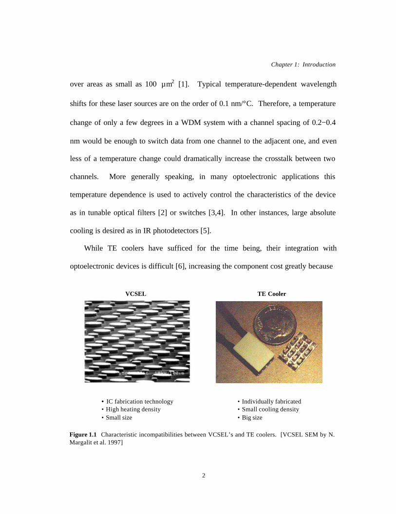
While TE coolers have sufficed for the time being, their integration with
optoelectronic devices is difficult [6], increasing the component cost greatly because
• IC fabrication technology• High heating density• Small size
• Individually fabricated• Small cooling density• Big size
VCSEL TE Cooler
Figure 1.1 Characteristic incompatibilities between VCSEL’s and TE coolers. [VCSEL SEM by N.Margalit et al. 1997]

Chapter 1: Introduction
3
of packaging. Figure 1.1 illustrates the incompatibilities between TE coolers and
VCSEL’s as an example. The reliability and lifetime of packaged modules can also
in some cases be limited by the TE cooler [7]. An alternative solution to thermal
management needs is to incorporate heterostructure integrated thermionic (HIT)
refrigerators with optoelectronic devices [8,9]. These thin film coolers use the
selective thermionic emission of hot electrons over a heterostructure barrier layer to
increase the cooling power beyond what can be achieved with the bulk
thermoelectric properties (see Figure 1.2). This enhanced evaporative cooling occurs
since the hot electrons that are on one side of the Fermi energy are emitted. In order
to maintain the quasi equilibrium Fermi distribution, lower energy electrons absorb
thermal energy from the lattice at the junction. The emitted electrons then redeposit
their energy after passing over the barrier. Since these thin film coolers can be made
with conventional III−V semiconductor materials, low-cost monolithic-integration
Vd
φC
φH
Figure 1.2 Conduction band diagram of a heterostructure integrated thermionic (HIT) cooler underan applied bias.

Chapter 1: Introduction
4
with optoelectronics is possible. Furthermore, standard integrated-circuit batch-
fabrication techniques can be used to manufacture these coolers, whereas TE coolers
use a bulk fabrication process.
In this chapter, current solid state cooler technology is first reviewed to illustrate
the merits of various approaches to increasing cooling capabilities. The second
section will discuss the motivation for moving from bulk (thick) coolers to thin-film
structures. Finally, the major contributions of this work will be outlined in the scope
of this thesis.
1.1 Current Solid State Cooler Technology
There is an increasing push to improve the figure of merit for thermoelectric
materials. This figure of merit is given by the dimensionless term ZT = (S2σ /κ)T,
where S is the Seebeck coefficient, σ and κ are the electrical and thermal
conductivities, respectively, and T is the ambient temperature (see Appendix A).
The best thermoelectric materials have a value of ZT ≈ 1 over a given temperature
range as illustrated in Figure 1.3. This value has been an upper limit for over 30
years, yet mysteriously no theoretical reason exists to answer why it can’t be larger.
With the advent of new theories, materials, and analysis capabilities, it is predicted
that this limit will be breached in the near future. Already, new theoretical
predictions are indicating that indeed a higher ZT is possible, and initial
experimental work is beginning to surface to validate these claims [10, 11]. Larger

Chapter 1: Introduction
5
0.0
0.2
0.4
0.6
0.8
1.0
1.2
0 200 400 600 800 1000 1200 1400
Bi2Te3
PbTeSiGe
BiSb B=0.2TZ
T
Temperature (K)
Figure 1.3 ZT’s of various thermoelectric materials versus temperature.
0
0.1
0.2
0.3
0.4
0.5
0 1 2 3 4 5
Figure 1.4 Fraction of Carnot efficiency versus the ZT of thermoelectrics. ZT’s greater than 3 willbe required to begin competing with conventional CFC cooling systems.
Typical CFC Systems
Next Generation TE’s?
Current TE’s
Frac
tion
of C
arno
t Eff
icie
ncy
ZT

Chapter 1: Introduction
6
ZT’s will not only benefit cooling of electronics and optoelectronics, but may
eventually allow solid-state cooling to compete with the more efficient CFC systems.
Figure 1.4 shows how the ZT of thermoelectrics is related to the fraction of Carnot
efficiency, which is the theoretical maximum efficiency possible. A ZT of at least
three will be needed to compete with the efficiencies of CFC systems.
1.1.1 Bulk Thermoelectric Materials
The fundamental problem for a good TE material is that it must have a high electrical
conductivity and at the same time a low thermal conductivity. However, in most
solids these two physical properties are related, similar to the Wiedemann-Franz
ratio in metals [12]. The ideal material possesses the poor thermal properties of glass
and the excellent electronic properties of a crystal. Skutterudites, clathrates, and
other open cage structures may possess these features [13, 14]. These compounds
have cage-like crystal structures in which the spaces are filled with atoms that can
effectively rattle around. This motion interferes with the conduction of heat but not
electricity, making them ideal candidates for the next generation of bulk
thermoelectrics. Rare-earth compounds and intermetallics are another group of
potential thermoelectric materials that are being explored for their large Seebeck
coefficients [15, 16]. While these new breeds of materials are a good direction for
TE cooler research, their application to integrated cooling still suffers from the same
problems discussed previously.
Chapter 1: Introduction
7
1.1.2 Micro-Thermoelectrics
Micro-thermoelectrics are a step closer in the direction of a practical cooler
technology for integrated applications. This body of research explores the concept of
making much smaller thermoelectric coolers with more advanced processing
techniques. The smallest conventional bulk coolers typically have a thermoelement
thickness on the order of a few millimeters, while micro-thermoelectrics can be
loosely categorized into thick film (~100’s µm) and thin film (~ 1-10 µm) structures.
The materials used are commonly conventional thermoelectric materials such as
BiTe or SiGe whose thermoelectric properties are well known, and where the
challenge lies with processing the device. Many different techniques have been
employed to miniaturize the cooler including electrochemical deposition [17],
extrusion [18], micro-fabrication of thick [6, 19, 20] and thin [21, 22] films to name
a few. Several of these techniques have produced working prototypes, with the thick
film devices typically demonstrating superior performance. This is due to the
increased non-ideal effects such as contact resistance and substrate thermal
resistance. The motivation for continuing to pursue thin-film structures in the
presence of these non-ideal effects will be discussed in Section 1.2.
Despite the infancy of micro-thermoelectric processing technology, several
commercially available products do exist. Cooling capacities on the order of 1 Watt
over areas as small as 3mm2 have been achieved using high conductive thermal
substrates and optimized contact resistances as low as 10-6 Ωcm2 [23, 24].

Chapter 1: Introduction
8
1.1.3 Lower Dimensional Structures
The development of thin film epitaxy, quantum wire, and quantum dot growth
techniques have opened the door to a new class of thermoelectric materials. Just as
the benefits of lower dimensional structures have advanced the electronic and
photonic industries, so too have they allowed for novel approaches to improving
solid-state cooling [25-27].
As the dimensionality is reduced, the electronic density of states accumulates
near the subband transitions. With appropriate doping, step changes and even delta
changes in available states for electrons result in a strong asymmetry in the
differential conductivity [28, 29]. The consequence of this strong asymmetry is an
enhanced thermopower which corresponds to the numerator of the ZT factor. Figure
1.5 depicts the density-of-states (DOS) versus energy in the 1-D, 2-D, and 3-D
regimes. The optimum transport distribution has been shown to be a Dirac delta
function centered about 2-3 kBT above or below the Fermi energy [30]. Further
discussion of the differential conductivity as it relates to thermoelectrics and
thermionics will follow in Chapter 2.
When designing lower dimensional structures, superlattices are typically used
since they provide the additional benefit of reducing the thermal conductivity [31-
33], i.e. the denominator of the ZT factor. With careful design of the materials,
thickness, and period of the superlattices, phonon-blocking electron-transmitting
structures can be realized [34].

Chapter 1: Introduction
9
The advantages of heterostructure thermionic cooling can be combined with that
of lower dimensional structures by using multi quantum-well structures. The added
constraint on the number of available electronic states should provide additional
electron filtering and further improve the thermopower.
1.2 Motivation for Thin Film Coolers
A distinct advantage of thin film coolers is the dramatic gain in cooling power
density as it is inversely proportional to the length of the thermoelements. Thin films
on the order of microns should provide cooling power densities greater than 1000
W/cm2. This capability for large cooling capacities is paramount for cooling of
optoelectronic devices. Another convenience of thin films is that they allow for the
DOS
2 D
1 D
0 DEner
gy
Figure 1.5 The electronic density of states (DOS) versus energy for various dimensionalities (3D,2D, 1D, and 0D). The first two quantified states are plotted.

Chapter 1: Introduction
10
possibility of monolithic integration. Besides the lower cost and higher reliability,
monolithic integration enables precise control over temperature anywhere on the
surface of the substrate where the devices to be cooled are located. The small
thermal mass of the cooler also permits a very fast cooling response.
Several disadvantages also become apparent and must be considered when
moving from bulk to thin film coolers. The most evident is the reduction in the
thermal resistance between the cold and hot side of the cooler. The trade-off for
increased cooling power is a reduced temperature differential and efficiency. Other
non-ideal effects such as contact resistance, thermal resistance of the heat sink, and
heat generation in the current carrying connections are secondary effects in bulk TE
coolers, but they all must be considered for thin film coolers [35].
1.3 Scope of Thesis
This thesis presents the first comprehensive examination of a novel type of micro-
cooler for integrated cooling applications. Using the established foundation of
theory and first generation cooler design that had been completed prior to this work
[9,36], the first semiconductor-based thermionic-emission cooler has been
demonstrated and is described in this thesis. From this first generation of coolers,
the results obtained drove continued theoretical and experimental work in cooler
development and integration with optoelectronic devices. In addition, the first
demonstration of integrated cooling with optoelectronics has also been achieved.

Chapter 1: Introduction
11
Parallel to the cooler research, advances in micro-scale temperature measurement
techniques were developed. Great progress has also been made in the optimization
of packaging, reduction of electrical contact resistance, and substrate transfer of thin
films.
In Chapter 1, motivation for this work and an overview of relevant
thermoelectric research was presented. Chapter 2 discusses more thoroughly the
microscopic origins of the Peltier effect and presents a theory of thermionic cooling
in heterostructures. From this theory, design guidelines are developed for the
specific cooler structures which are discussed in Chapter 3. Chapter 4 examines the
pertinent material properties and the techniques to measure them. The evolution of
the device fabrication and packaging is presented in Chapter 5. Chapter 6 discusses
measurement techniques and the experimental results and analysis. Chapter 7
presents several examples of the integration of heterostructure thermionic emission
coolers with optoelectronic devices. Finally, Chapter 8 concludes with a review of
the highlights from each chapter and suggestions for future work.
In summary, this thesis examines the novel approach of thermionic emission in
heterostructures for enhanced cooling beyond the bulk properties of the materials,
and the application of this technology to the integration of active cooling with
optoelectronic devices.

Chapter 1: Introduction
12
REFERENCES
1. J. Piprek, Y.A. Akulova, D.I. Babic, L.A. Coldren, J.E. Bowers, “Minimum temperaturesensitivity of 1.55 µm vertical-cavity lasers at 30 nm gain offset,” Appl. Phys. Lett., Vol. 72, No.15, (13 April 1998), pp. 1814-6.
2. J. Hukriede, D. Kip, E. Kratzig, “Thermal tuning of a fixed Bragg grating for IR light fabricatedin a LiNbO3:Ti channel waveguide,” Appl. Phys. B, Vol 70, (2000), pp. 73-5.
3. Y. Baek, R. Schiek, G.I. Stegeman, “All-optical switching in a hybrid Mach-Zehnderinterferometer as a result of cascaded second-order nonlinearity,” Optics Lett., Vol. 20, No. 21, (1Nov. 1995), pp.2168-70.
4. X. Lu, D. An, L. Sun, Q. Zhou, R.T. Chen, “Polarization-insensitive thermo-optic switch basedon multimode polymeric waveguides with an ultralarge optical bandwidth,” Appl. Phys. Lett.,Vol. 76, No. 16, (17 April 2000), pp. 2155-7.
5. J. Piotrowski, C.A. Musca, J.M. Dell, L. Faraone, “Infrared Photodetectors Operating at NearRoom Temperature,” Proceedings of Conference on Optoelectronic and MicroelectronicMaterials and Devices, Perth, WA, Australia, Dec. 1998, pp. 124-7.
6. L. Rushing , A. Shakouri, P. Abraham, J.E. Bowers, “Micro thermoelectric coolers for integratedapplications,” Proceedings of the 16th International Conference on Thermoelectrics, Dresden,Germany, August 1997, pp. 646-9.
7. T.A. Corser, “Qualification and reliability of thermoelectric coolers for use in laser modules,” 41st
Electronic Components and Technology Conference, Atlanta, GA, USA, May 1991, pp. 150-6.
8. A. Shakouri, C. LaBounty, J. Piprek, P. Abraham, J.E. Bowers, “Thermionic emission cooling insingle barrier heterostructures,” Appl. Phys. Lett., Vol. 74, No.1, (4 Jan. 1999), pp. 88-89.
9. A. Shakouri, E.Y. Lee, D.L. Smith, V. Narayanamurti, J.E. Bowers, “Thermoelectric effects insubmicron heterostructure barriers,” Microscale Thermophysical Engineering, Vol 2, No. 37,1998.
10. Proceedings of the 19th International Conference on Thermoelectrics, Cardiff, Wales, UnitedKingdom, 20-24th August 2000.
11. Thermoelectric Materials 2000 – The Next Generation Materials for Small-Scale Refrigerationand Power Generation Applications, edited by T.M. Tritt, G.S. Nolas, G.D. Mahan, D. Mandrus,M.G. Kanatzidis, Materials Research Society Symposium Proceedings, Vol. 626, April 2000.
12. C. Kittel, Introduction to Solid State Physics. New York: Wiley, 1996.
13. G.S. Nolas, M. Kaeser, R.T. Littleton, T.M. Tritt, H. Sellinschegg, D.C. Johnson, E. Nelson,“Partially-Filled Skutterudites: Optimizing the Thermoelectric Properties ,” Materials ResearchSociety Symposium Proceedings, Vol. 626, April 2000.
Chapter 1: Introduction
13
14. N.P. Blake, L. Mollnitz, G. Kresse, H. Metiu, “Why clathrates are good thermoelectrics: Atheoretical study of Sr8Ga16Ge30,” Journal of Chemical Physics, Vol. 111, No.7, 15 Aug. 1999,p.3133-3144.
15. G.D. Mahan, “Rare Earth Thermoelectrics,” Proceedings of the 16th International Conference onThermoelectrics, Dresden, Germany, August 1997, pp. 21-24.
16. C. Uher, J. Yang, G.P. Meisner, “Thermoelectric Properties of Bi-Doped Half-Heusler Alloys,”Proceedings of the 18th International Conference on Thermoelectrics, Baltimore, MD, USA, 29Aug.-2 Sept. 1999, p.56-9.
17. J.P. Fleurial, G.J. Snyder, J.A. Herman, P.H. Giauque, W.M. Phillips, M.A. Ryan, P. Shakkottai,E.A. Kolawa, M.A. Nicolet, “Thick-Film Thermoelectric Microdevices,” Proceedings of the 18th
International Conference on Thermoelectrics, Baltimore, MD, USA, 29 Aug.-2 Sept. 1999,p.294-300.
18. V. Semenyuk, J.G. Stockholm, F. Gerard, “Thermoelectric Cooling of High Power ExtremelyLocalized Heat Sources: System Aspects,” Proceedings of the 18th International Conference onThermoelectrics, Baltimore, MD, USA, 29 Aug.-2 Sept. 1999, p.40-44.
19. M. Kishi, H. Nemoto, M. Yamamoto, Y. Yoshida, “Fabrication of a Miniature ThermoelectricModule with Elements Composed of Sintered Bi-Te Compounds,” Proceedings of the 16th
International Conference on Thermoelectrics, Dresden, Germany, August 1997, pp. 653-6.
20. E. Yu, D. Wang, S. Kim, A. Przekwas, “Active Cooling of Integrated Circuits and OptoelectronicDevices Using a Micro Configured Thermoelectric and Fluidic System,” Proceedings of the 7th
Intersociety Conference on Thermal and Thermomechanical Phenomena in Electronic Systems,Las Vegas, NV, USA, 23-26 May 2000, Vol.2 p.134-9.
21. I. Stark, M. Stordeur, “New micro thermoelectric devices based on bismuth telluride-type thinsolid films,” Proceedings of the 18th International Conference on Thermoelectrics, Baltimore,MD, USA, 29 Aug.-2 Sept. 1999, p.465-72.
22. A. Giani, A. Boulouz, F. Pascal-Delannoy, A. Foucaran, E. Charles, A. Boyer, “Growth of Bi2Te3
and Sb2Te3 thin films by MOCVD,” Materials Science and Engineering B, B64, (1999), p. 19-24.
23. V. A. Semenyuk, T.V. Pilipenko, G.C. Albright, L.A. Ioffe, W.H. Rolls, “MiniatureThermoelectric Coolers for Semiconductor Lasers,” Proceedings of the 13th InternationalConference on Thermoelectrics, Kansas City, MO, USA, 1994, p.150-153.
24. M. Kishi, H. Nemoto, T. Hamao, M. Yamamoto, S. Sudou, M. Mandai, S. Yamamoto, “Micro-Thermoelectric Modules and Their Application to Wristwatches as an Energy Source,”Proceedings of the 18th International Conference on Thermoelectrics, Baltimore, MD, USA, 29Aug.-2 Sept. 1999, p.301-307.
25. L. D. Hicks, M. S. Dresselhaus, “Experimental study of the effect of quantum-well structures onthe thermoelectric figure of merit,” Physical Review B (Condensed Matter), vol.53, pp. R10493-10496, 1996.

Chapter 1: Introduction
14
26. T. Koga, X. Sun, S.B. Cronin, M.S. Dresselhaus, “Carrier pocket engineering applied to strainedSi/Ge superlattices to design useful thermoelectric materials,” Applied Physics Letters, Vol. 75,No.16, 18 Oct 1999, p.2438-40.
27. T. C. Harman, D. L. Spears, M. J. Manfra, “High thermoelectric figures of merit in PbTequantum wells,” Journal of Electronic Materials, vol.25, pp. 1121-1127, 1996.
28. A. Shakouri, C. LaBounty, “Material Optimization for Heterostructure Integrated ThermionicCoolers,” Proceedings of the 18th International Conference on Thermoelectrics, Baltimore, MD,USA, 29 Aug.-2 Sept. 1999, p.35-39.
29. D.A. Broido, T.L. Reinecke, “Thermoelectric power factor in superlattice systems,” AppliedPhysics Letters, Vol. 77, No.5, 31 July 2000, p. 705-7.
30. J.O. Sofo, G.D. Mahan, “The best thermoelectric,” Proceedings of the National Academy ofScience, USA, Vol. 93, 1996, pp. 7436-7439.
31. G. Chen, “Thermal conductivity and ballistic-phonon transport in the cross-plane direction ofsuperlattices,” Phys. Rev. B (Condensed Matter), Vol.57, (1998), pp. 14958-73.
32. P. Hyldgaard, G.D. Mahan, “Phonon superlattice transport,” Phys. Rev. B , Vol.56, No.17, (1997),pp. 10754-57.
33. R. Venkatasubramanian, “Lattice thermal conductivity reduction and phonon localizationlikebehavior in superlattice structures,” Phys. Rev. B , Vol.61, No.4, (2000), pp. 3091-7.
34. R. Venkatasubramanian, “Phonon-Blocking Electron-Transmitting Structures,” Proceedings ofthe 18th International Conference on Thermoelectrics, Baltimore, MD, USA, 29 Aug.-2 Sept.1999, p.100-3.
35. C. LaBounty, A. Shakouri, J.E. Bowers, “Design and characterization of thin film microcoolers,”Journal of Applied Physics, Vol. 89, No.7, 1 April 2001, p.4059-64.
36. A. Shakouri, J.E. Bowers, “Heterostructure integrated thermionic coolers,” Appl. Phys. Lett., Vol.71, No.9, (1997), pp. 1234-6.

Chapter 2: Thermionic Emission in Heterostructures
15
Chapter 2
Thermionic Emission in Heterostructures
The idea of thermionic energy conversion was first seriously explored in the mid-
fifties during the development of vacuum diodes and triodes. Using a high work
function cathode in contact with a heat source, electrons are emitted (thermionic
emission process) and are absorbed by a cold, low work function anode. The
electrons then flow back to the cathode through an external load where they perform
useful work. Practical thermionic generators are limited by the work function of
available materials that are used for cathodes. Another important limitation is the
space charge effect, where the presence of charged electrons in the space between
cathode and anode creates an extra potential barrier, reducing thermionic current.
Various means of reducing this space charge effect were proposed to improve the
efficiency of thermionic generators, such as close-spacing of the cathode and anode,
or the use of a third positive electrode to counteract space charge. A major advance
in the field occurred in 1957 when the introduction of positive ions (cesium vapor) in
the inter-electrode space eliminated the need for the close spacing and resulted in
substantial improvements in performance. The materials currently used for cathodes
have work functions greater than 0.7 eV which limits the applications to high
temperatures greater than 500K. Recently, these vacuum diode thermionic
generators were proposed for refrigeration [1]. Efficiencies over 80% of the Carnot

Chapter 2: Thermionic Emission in Heterostructures
16
value were predicted, but the operating temperatures are still limited to greater than
500K.
Even more recently, thermionic emission cooling in heterostructures was
proposed by Shakouri et al. [2] to overcome the limitations of vacuum thermionics at
lower temperatures. With current epitaxial growth techniques such as molecular
beam epitaxy (MBE) or metal-organic chemical vapor deposition (MOCVD), precise
control over layer thickness and composition is possible. In conjunction with
bandgap engineering, these techniques allow for the design of a new class of
semiconductor thermionic emission devices with improved cooling capacities.
Using various material systems such as GaAs/AlGaAs, InP/InGaAsP, Si/SiGe,
structures with barrier heights of 0.0 to 0.5 eV can be grown reliably. In this case,
the barrier height is determined by the band edge discontinuity between heterolayers.
Depending on growth constraints and lattice mismatch between materials, it is
possible to grade the barrier composition to construct internal fields and to enhance
electron transport properties. Close and uniform spacing of cathode and anode is no
longer an issue and can be achieved with atomic resolution. The problem of space
charge, if it arises, can be controlled by modulation doping in the barrier region.
In this chapter, an intuitive picture of thermoelectric and thermionic cooling in
semiconductors is first presented. From this basis, the concept of thermionic
emission cooling is more fully examined and the design of optimized structures
explored.

Chapter 2: Thermionic Emission in Heterostructures
17
2.1 Intuitive Picture of Thermoelectrics and Thermionics
The expressions for electrical conductivity and Seebeck coefficient can be
written as [3-5]:
where we introduce the "differential" conductivity:
Here τ(E) is the energy dependent relaxation time, v x ( E ) the average velocity of
the carriers with energy between E and E+dE in the direction of current flow, and
n x ( E ) the number of electrons in this energy interval. Electrical conductivity is the
sum of the contribution of electrons with various energies E (given by σ(E) the
>−∝<−
−−
≡
−
−−=
−≡
−=
∫
∫
∫∫∫
∫∫∫
∫
∫∫∫
feq
eq
B
F
B
eqx
eqFx
eq
eqx
EEdE
Ef
E
dEEf
TkEE
E
ek
kdEf
kvk
kdEf
EkEkvk
eTS
dEE
fE
kdEf
kvke
)()(
)()(
)(
)()()(
)())()(()(1
)()(
)()()(4
32
32
323
2
∂∂
σ
∂∂
σ
∂∂
τ
∂∂
τ
∂
∂σ
∂∂
τπ
σ (2.1)
(2.2)
)()()(),,()()( 2222 EnEvEedkdkkkEvEeE xzyzyx ττσ ≅≡ ∫∫ (2.3)

Chapter 2: Thermionic Emission in Heterostructures
18
differential conductivity) within the Fermi window factor ?feq/?E. The Fermi
window is a direct consequence of the Pauli exclusion principle, and at finite
temperatures only electrons near the Fermi surface contribute to the conduction
process. In this picture the Seebeck coefficient described in Equation 2.2 is the
average energy transported by the charge carriers corresponding to a diffusion
thermopower. This transported energy can be increased with the coupling of other
energy transport mechanisms such as phonons to the electronic transit. As
mentioned in Chapter 1, the overall device performance in conventional
thermoelectric coolers is given by the dimensionless figure of merit ZT = S2σT / β ,
that describes the tradeoffs between the Peltier cooling given by the Seebeck
coefficient (S), the Joule heating given by the electrical conductivity (σ), and the heat
conduction from the hot to cold junction given by the thermal conductivity (β). It is
this Z-factor that must be maximized to reach optimum performance and efficiency.
At room temperature, conventional semiconductors have a thermal conductivity that
is dominated by the lattice contribution, therefore maximizing Z necessitates
maximizing the power factor S2σ ≈ |⟨E − Ef⟩|2σ. Hence the differential conductivity,
σ(E), should be large within the Fermi window and be as asymmetric as possible
with respect to the Fermi energy.
The microscopic origin of the Peltier effect can be described as follows: When
electrons move from a material in which their average transport energy is below the
Fermi level, to another one in which their transport energy is increased, the electron

Chapter 2: Thermionic Emission in Heterostructures
19
gas will absorb thermal energy from the lattice and the junction between the two
materials will be cooled (see Fig. 2.1). Reversing the direction of current will
instead generate heat and will create a hot junction signifying a reversible heat
engine.
2.1.1 Lower Dimensional Structures Revisited
From the discussion above, the perceived advantage of moving to lower-dimensional
semiconductor structures can be better explained than in Chapter 1. The number of
electronic states in each energy interval is increased when the dimensionality is
reduced, and at the same time the DOS “accumulates” near the subband edges, which
DistributionFunction
Ef
Density ofStates
Energy
1
σ(E)
E
Differential Conductivity
σ’(E)
E
Material (a) Material (b)
Cooling atthe Junction
(a) (b)
Figure 2.1 (a) Energy versus density of states and Fermi distribution function for a degeneratelydoped n-type semiconductor. (b) The energy distribution of electrons moving in the semiconductorunder an electric field is given by σ(E) the differential conductivity that determines the averagetransport energy of carriers. As the average transport energy increases from material “a” to material“b”, thermal energy is absorbed from the lattice and the junction is cooled.

Chapter 2: Thermionic Emission in Heterostructures
20
increases the asymmetry in σ(E) if a proper doping is chosen. Recent literature on
quantum well and wire thermoelectrics [6-9] emphasized the increased DOS, but the
symmetry is not mentioned and its consequences are buried in the calculations of
optimum doping in these structures. The symmetry of σ(E) is the main cause of low
thermopower in metals, even though they have a very large DOS.
Considering practical cooling applications, the advantages of using electron
transport parallel to heterostructures is diminished by the finite thermal conductance
of inactive barrier layers and other non-ideal effects [8-9,15]. Using bandstructure
engineering, heterostructures can be designed that modify not only the DOS, but also
the electron velocity and relaxation times. Based on these concepts, electron
transport perpendicular to the quantum wells was proposed to reduce the mobility of
low energy or “cold” electrons and to increase the thermopower [10-12]. A problem
arises however, when only the effect of the DOS is considered in the mini-band
conduction regime. Increasing the asymmetry of the DOS essentially means
reducing ∂E/∂k. However this reduction also results in a reduced electron velocity
since it is also proportional to the band curvature ∂E/∂k. Looking at Equation 2.3,
these two effects are seen to be opposing each other, diminishing the benefits of
asymmetry in σ(E).
All of these lower-dimensional concepts and primary calculations are based on
the linearized Boltzmann transport equation which is valid in the band conduction
regime and when the electronic distribution function is not changed considerably
Chapter 2: Thermionic Emission in Heterostructures
21
with respect to the Fermi distribution. The application of heterostructures for
thermoelectric cooling goes beyond the Boltzmann transport regime, complicating
the theoretical analysis further.
2.1.2 Material Optimization for Traditional Thermoelectrics
By optimizing the doping in the expressions for electrical conductivity and Seebeck
coefficient, one can find that the following ratio of material parameters needs to be
optimized [3-5,13,14]:
The dependence on electron mobility in the material figure-of-merit expression
reflects the importance of unimpeded electron transport in the material to reduce the
Joule heating. The requirement for large effective mass is due to the symmetry of
the electronic density-of-states with respect to the Fermi energy over an energy range
that is on the order of thermal energy (kBT). The asymmetry may be increased by
doping the material such that the Fermi level is close to the band edge, however this
results in a small number of electrons taking part in conduction and a small amount
of heat transported.
The trade off between Seebeck coefficient and conductivity versus doping is
illustrated in Figure 2.2. As the doping is increased, the Seebeck coefficient
decreases while the conductivity increases. The decline in Seebeck coefficient can
⋅ 5.2
5.1*.CT
mβ
µ (2.4)

Chapter 2: Thermionic Emission in Heterostructures
22
be explained by the reduced asymmetry in the DOS. Looking again at Figure 2.1, as
the doping is increased and the Fermi level moves upward in energy, the DOS
becomes more vertical and changes little above and below the Fermi energy. At
these high doping densities, the situation is similar to the case of metals. Since the
Fermi energy is deep inside the band, there are almost as many electrons above the
Fermi energy as below, so the average energy of the moving electron gas under an
electric field is very close to the Fermi level. The rise in the conductivity is simply a
result of more carriers being present, even despite the reduction in electron mobility
due to charged impurity scattering. The product of S2⋅σ then gives the power factor
versus doping, or the ZT after being divided by the thermal conductivity and
multiplied by temperature.
0 10 0
100 10 -6
200 10 -6
300 10 -6
400 10 -6
0.0 100
1.0 105
2.0 105
3.0 105
4.0 105
1017 1018 1019
Doping (cm-3)
Seeb
eck
Coe
ffic
ient
(V/K
)
Electrical Conductivity (1/Ω
cm)
Figure 2.2 Calculation of Seebeck coefficient (S) and electrical conductivity (σ ) as a function ofdoping for InGaAs bulk material. The substantial decrease in S at high dopings and σ at lowdopings is the cause of low power factor and thus poor ZT.

Chapter 2: Thermionic Emission in Heterostructures
23
2.1.3 Thermionic Emission Cooling in Heterostructures
Another more promising way to increase the asymmetry of σ(E) is to use
thermionic emission in heterostructures. Using conduction (n-type) or valence (p-
type) band offsets at heterointerfaces, the transport energy of electrons can be made
to be almost entirely on one side of the Fermi level resulting in strong asymmetry
[1,10-11,16-21]. In a simplified model [16-17] that neglects the finite electron
energy relaxation length, the maximum cooling temperature by heterostructure
thermionic emission can be expressed as:
where Tc is the cold side temperature, Φc the cathode barrier height, I the current, λ
the electron mean free path in the barrier, and β the thermal conductivity of the
barrier layer. By maximizing this equation with respect to current, the material
dependence of ∆Tmax is determined to be only through the ratio λm*/β or
µm*1.5/β , where µ is the carrier mobility in the barrier region.
Interestingly, in this approximation, thermionic emission cooling and thermoelectric
cooling have the same material figure of merit (Equation 2.4), and so through
−
+
Φ+=∆ 12
),(2
12
max ITk
TIeekTT
CB
CCBC β
λ (2.5)
−⋅⋅+=∆ 1
.238
1 5.25.1*
3
5.3
maxmax
CB
CIT
mehk
TTβ
µπ(2.6)
Chapter 2: Thermionic Emission in Heterostructures
24
selective emission of hot carriers in heterostructures we can improve the cooling
capacity of conventional thermoelectric materials.
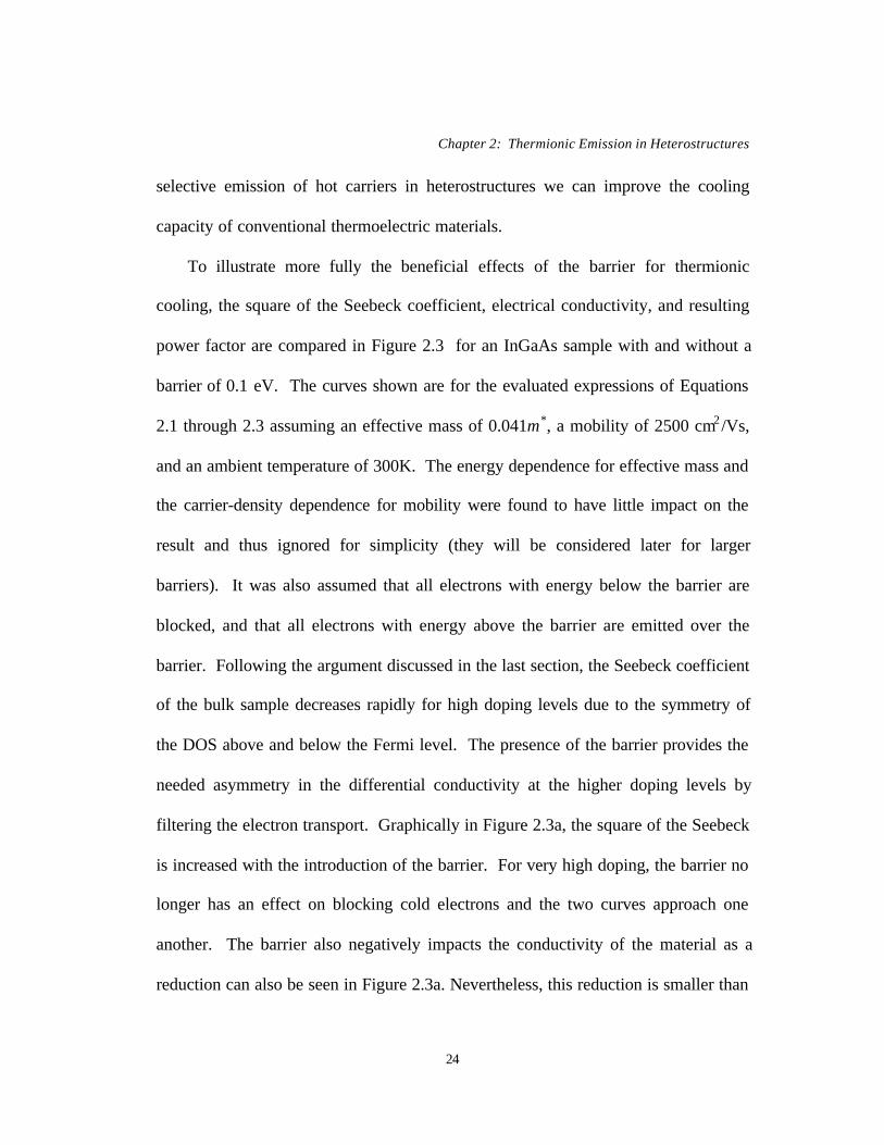
To illustrate more fully the beneficial effects of the barrier for thermionic
cooling, the square of the Seebeck coefficient, electrical conductivity, and resulting
power factor are compared in Figure 2.3 for an InGaAs sample with and without a
barrier of 0.1 eV. The curves shown are for the evaluated expressions of Equations
2.1 through 2.3 assuming an effective mass of 0.041m*, a mobility of 2500 cm2 /Vs,
and an ambient temperature of 300K. The energy dependence for effective mass and
the carrier-density dependence for mobility were found to have little impact on the
result and thus ignored for simplicity (they will be considered later for larger
barriers). It was also assumed that all electrons with energy below the barrier are
blocked, and that all electrons with energy above the barrier are emitted over the
barrier. Following the argument discussed in the last section, the Seebeck coefficient
of the bulk sample decreases rapidly for high doping levels due to the symmetry of
the DOS above and below the Fermi level. The presence of the barrier provides the
needed asymmetry in the differential conductivity at the higher doping levels by
filtering the electron transport. Graphically in Figure 2.3a, the square of the Seebeck
is increased with the introduction of the barrier. For very high doping, the barrier no
longer has an effect on blocking cold electrons and the two curves approach one
another. The barrier also negatively impacts the conductivity of the material as a
reduction can also be seen in Figure 2.3a. Nevertheless, this reduction is smaller than
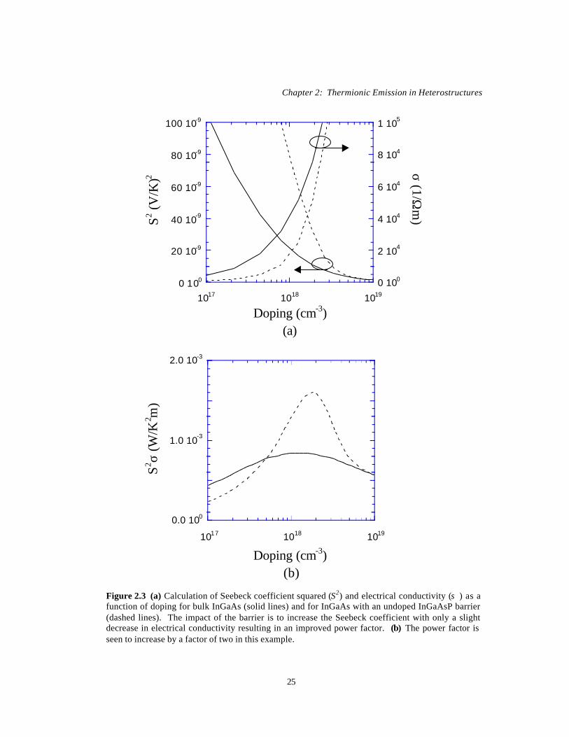
Chapter 2: Thermionic Emission in Heterostructures
25
0 100
20 10-9
40 10-9
60 10-9
80 10-9
100 10-9
0 100
2 104
4 104
6 104
8 104
1 105
1017 1018 1019
Doping (cm-3)
S2 (V/K
)2σ (1/Ω
m)
Figure 2.3 (a) Calculation of Seebeck coefficient squared (S2) and electrical conductivity (σ ) as afunction of doping for bulk InGaAs (solid lines) and for InGaAs with an undoped InGaAsP barrier(dashed lines). The impact of the barrier is to increase the Seebeck coefficient with only a slightdecrease in electrical conductivity resulting in an improved power factor. (b) The power factor isseen to increase by a factor of two in this example.
0.0 100
1.0 10-3
2.0 10-3
1017 1018 1019
Doping (cm-3)
S2 σ (W
/K2 m
)
(a)
(b)

Chapter 2: Thermionic Emission in Heterostructures
26
the increase in Seebeck coefficient and the overall power factor is approximately
doubled as shown in Figure 2.3b.
2.2 N-type and P-type Structures
The concept of filtering electrons with barriers in n-type material that has been
presented so far also applies to the filtering of holes in p-type material as illustrated
in Figure 2.4. Just as the barrier in the conduction band passes high energy (hot)
electrons and blocks low energy (cold) electrons, an analogous barrier in the valence
band can pass high energy holes while blocking low energy holes. It is important to
note that for the same bias polarity, the n-type device cools on the left side and heats
on the right whereas the p-type device heats on the left and cools on the right. This
is fortunate since it lets us imitate the conventional thermoelectric configuration of
multi n- and p-type elements connected electrically in series and thermally in
parallel. This arrangement has several advantages over the single element case. It
first allows for the removal of the external electrical connection to the cold side of
the device and keeps all external connections on the hot side, close to the heat sink.
The other main advantage is in reducing the necessary external current bias. A large
area thermoelement (length & width >> thickness) requires a much larger current
than a small area thermoelement (length & width ~ thickness) to maintain the same
temperature difference. By placing many of the small area thermoelements together,
it is still possible to cool an area that is the same size as the large area

Chapter 2: Thermionic Emission in Heterostructures
27
thermoelement. Correspondingly, as the individual elements are made smaller, the
required current is reduced and the external voltage is increased.
2.3 Design of Barriers for Cooling
Now that the microscopic thermoelectric and thermionic cooling mechanisms have
been discussed, the question of how to optimally design these structures remains.
φBn
Figure 2.4 (a) Conduction band diagram of a n-type and (b) a valence band diagram of a p-typethermionic emission cooler under an applied bias V. For the same bias polarity, the n-type devicecools on the left and heats on the right, while the p-type device heats on the left and cools on theright.
V
φBp
EC
EV
cold
hothot
cold
e
h
(a)
(b)

Chapter 2: Thermionic Emission in Heterostructures
28
This section will be devoted to presenting and discussing the design issues and
guidelines for thermionic emission coolers.
2.3.1 Band Gap Engineering
The band gap engineering of the thermionic cooler structures takes into consideration
many of the same issues as thermoelectrics. In the most ideal case of designing a
solid-state cooling medium, the following three effects must be considered: cooling
power; Joule heating; and heat conduction. Taking into account these effects, the
overall cooling capacity of a single barrier thermionic cooler with cathode-side
barrier height ΦC, barrier thickness d, cross-sectional area A, and thermal
conductivity β , can be expressed as [2]:
where kB is the Boltzmann constant, e the electron charge (not to be confused with
the exponential in the second term), λE the energy relaxation length for carriers, TC
the cold side (cathode) temperature, and ∆T=TH – TC. The anode barrier height is
not considered in the above approximation, and it is simply assumed to be high
enough to suppress the reverse current from the hot to cold side. The first term of
Equation 2.7 describes the thermionic cooling power which can be explained as the
total current times the average energy of the carriers that are emitted over the barrier.
( ) TdA
edd
IVIeTk
Q EdEECBCTI ∆−
−−
−−⋅
+Φ= − βλλ λ 1
21
2 /2
2
(2.7)
Chapter 2: Thermionic Emission in Heterostructures
29
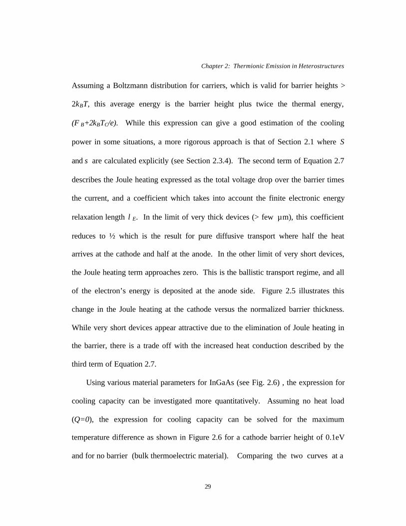
Assuming a Boltzmann distribution for carriers, which is valid for barrier heights >
2kBT, this average energy is the barrier height plus twice the thermal energy,
(ΦB+2kBTC/e). While this expression can give a good estimation of the cooling
power in some situations, a more rigorous approach is that of Section 2.1 where S
and σ are calculated explicitly (see Section 2.3.4). The second term of Equation 2.7
describes the Joule heating expressed as the total voltage drop over the barrier times
the current, and a coefficient which takes into account the finite electronic energy
relaxation length λE. In the limit of very thick devices (> few µm), this coefficient
reduces to ½ which is the result for pure diffusive transport where half the heat
arrives at the cathode and half at the anode. In the other limit of very short devices,
the Joule heating term approaches zero. This is the ballistic transport regime, and all
of the electron’s energy is deposited at the anode side. Figure 2.5 illustrates this
change in the Joule heating at the cathode versus the normalized barrier thickness.
While very short devices appear attractive due to the elimination of Joule heating in
the barrier, there is a trade off with the increased heat conduction described by the
third term of Equation 2.7.
Using various material parameters for InGaAs (see Fig. 2.6) , the expression for
cooling capacity can be investigated more quantitatively. Assuming no heat load
(Q=0), the expression for cooling capacity can be solved for the maximum
temperature difference as shown in Figure 2.6 for a cathode barrier height of 0.1eV
and for no barrier (bulk thermoelectric material). Comparing the two curves at a

Chapter 2: Thermionic Emission in Heterostructures
30
0
0.1
0.2
0.3
0.4
0.5
0.01 0.1 1 10 100 1000
d/λE
Frac
tion
of J
oule
Hea
t
Figure 2.5 Fraction of the Joule heating generated in the barrier that arrives to the cathode versusthe barrier thickness (d) normalized by the relaxation length for carriers (λE). The anode side of thebarrier is assumed to be in contact with an ideal heat sink.
0.01
0.1
1
10
100
102 103 104 105 106
J (A/cm2)
∆T
(K)
Figure 2.6 Cooling temperature as a function of current for InGaAs with (0.1 eV) and with out(bulk thermoelectric) a conduction band barrier. The electrical and thermal conductivities weremeasured experimentally, and the electron relaxation length was taken from previous work [18].
φC = 0.1 eV
Bulk TE
Tc=300K, meff/mo=0.41, µ=4500cm2/Vs,β=.06W/cmK, λE=0.4µm, d=1µm

Chapter 2: Thermionic Emission in Heterostructures
31
current density of 105 A/cm2, the maximum cooling of the bulk material is 5.5 K
while the barrier device is 24 K, more than a factor of four greater. In this
approximation, the maximum allowable current is limited by the thermionic emission
given by the Richardson thermionic emission expression [22]:
where A* is the effective Richardson constant. For an InGaAs barrier of 0.1eV, the
magnitude of the first term outside the brackets is approximately 7×10⁵ A/cm2. In
practical applications of such a cooler structure, non-ideal heating effects such as
contact resistance usually limits the optimum current density. Here we considered a
contact resistance of 5×10⁻⁸ Ωcm2, the lowest reported experimental value available
[23]. The other non-ideal factors that ultimately limit the optimum current bias will
be discussed in subsequent chapters.
2.3.2 Barrier Thickness
In designing thin film coolers, the thickness of the film plays an important role in the
device behavior. In any type of cooler there is the same relation between
temperature differential and cooling power, expressed as:
−
⋅
−= 1expexp2*
TkqV
Tkq
TAJBB
Cφ(2.8)
QRT th=∆ (2.9a)

Chapter 2: Thermionic Emission in Heterostructures
32
where Rth is the thermal resistance and βeff is the effective thermal conductivity. This
equation is analogous to the electrical equivalent Ohm’s Law, replacing temperature
for voltage, heat current for electrical current, and thermal resistance for electrical
resistance. The specific application of the cooler must be considered in the design as
to what temperature difference and cooling powers are required.
Continuing with the numerical analysis from the last section, the effect of barrier
thickness can be examined. Figure 2.7 plots the maximum cooling power,
temperature difference, and corresponding optimum current density versus barrier
thickness. Below 1µm, the cooling power and current density begin to saturate due
to contact Joule-heating effects while the temperature difference decreases owing to
the reduced thermal resistance. Above 1µm, the temperature difference becomes
independent of thickness, while the cooling power and current density decrease.
Herein lies the trade off between cooling power and the required current supply.
Basically it takes less current to maintain a certain temperature difference across a
thicker device since less compensation is needed to counteract the back flow of heat
to the cold side. Still, even with a 10µm thick barrier, the cooling power exceeds
8000 W/cm2 while only requiring about 10 kA/cm2. These orders of thickness
appear attractive, however severe difficulties arise in practically growing such
structures. Looking to Equation 2.9b, an alternative to increasing the thickness of the
Ad
Reff
th
β= (2.9b)

Chapter 2: Thermionic Emission in Heterostructures
33
102
103
104
105
106
0.1 1 10
1
10
100
0.1 1 10
104
105
106
107
0.1 1 10d (µm)
Q (W
)
Figure 2.7 (a) Maximum cooling power, (b) maximum cooling, and (c) the correspondingoptimum current as a function of barrier thickness for a 0.1 eV barrier and bulk thermoelectriceffect. A minimum contact resistance of 5x10⁻⁸Ωcm2 was used to bound the current to practicalvalues.
φC = 0.1 eV
Bulk TE
∆T
(K)
J (A
/cm
2 )
φC = 0.1 eV
Bulk TE
φC = 0.1 eV
Bulk TE
(a)
(b)
(c)

Chapter 2: Thermionic Emission in Heterostructures
34
barrier is to decrease its thermal conductivity. Using superlattice designs to reduce
the thermal conductivity is addressed in the next section.
2.3.3 Superlattice period
There are many issues to consider when designing the period of the superlattice. The
ultimate goal is to minimize the thermal conductivity while maintaining an
acceptable electrical conductivity, all while avoiding any impact on the cooling
properties of the barrier. The total thermal conductivity (βT) is the sum of both
lattice (βL) and electronic (βe) contributions. Luckily the picture is somewhat
simplified since for InP-based material systems with doping levels that we will
consider, the electronic contribution can be neglected.
The origin of the contribution of specific factors on the thermal conductivity in
superlattices is not completely clear. Detailed theoretical investigations using a
Boltzmann transport model [24,25] and other representations [26,27] have been
undertaken to explain thermal conductivity in superlattices. Several mechanisms
have been considered to explain the thermal transport including scattering of the
phonons at the interfaces due to roughness, defects, and dislocations, or phonon
wave localization and reflection originating from the impedance mismatch. The
resulting reduction in thermal conductivity from interface scattering can be attributed
to the reduced phonon mean free path (lmfp). From kinetic theory [28] the two
quantities can be related:

Chapter 2: Thermionic Emission in Heterostructures
35
where C is the heat capacity, and vavg is the average phonon velocity. However,
increasing the scattering at interfaces to decrease thermal conductivity may also have
the effect of significantly decreasing the electrical conductivity; an undesirable
result. In the InP-based material systems considered here, the superlattices are lattice
matched with high quality interfaces so that the interface scattering is minimized.
Hence any reduction in βL should come from phonon filtering analogous to the
optical distributed-Bragg-reflection, or from other phonon wave localization effects.
With the lack of an accurate theoretical model to calculate βL versus superlattice
period, an experimental approach must be taken to optimize these structures. The
starting point is to design the period close to the phonon mean free path to take
advantage of any wave-nature effects. Permutations about this initial superlattice
period can then be investigated in an attempt to minimize βL.
2.3.4 High Barrier Devices
In the previous discussion of thermionic cooling in heterostructures, we looked at the
cooling properties for a moderate barrier height of 100 meV using a Boltzman
approximation. Larger barrier heights will now be addressed with a more explicit
calculation and their merits discussed.
mfpavgL lCv31
=β (2.10)
Chapter 2: Thermionic Emission in Heterostructures
36
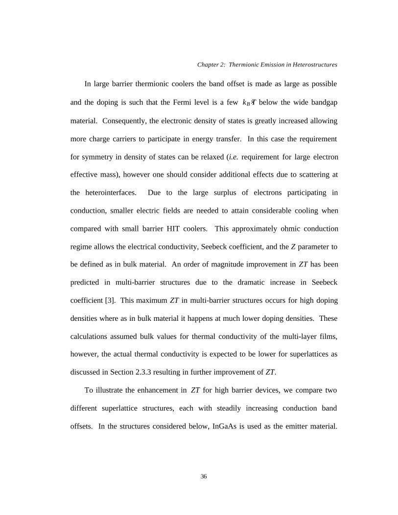
In large barrier thermionic coolers the band offset is made as large as possible
and the doping is such that the Fermi level is a few kB⋅T below the wide bandgap
material. Consequently, the electronic density of states is greatly increased allowing
more charge carriers to participate in energy transfer. In this case the requirement
for symmetry in density of states can be relaxed (i.e. requirement for large electron
effective mass), however one should consider additional effects due to scattering at
the heterointerfaces. Due to the large surplus of electrons participating in
conduction, smaller electric fields are needed to attain considerable cooling when
compared with small barrier HIT coolers. This approximately ohmic conduction
regime allows the electrical conductivity, Seebeck coefficient, and the Z parameter to
be defined as in bulk material. An order of magnitude improvement in ZT has been
predicted in multi-barrier structures due to the dramatic increase in Seebeck
coefficient [3]. This maximum ZT in multi-barrier structures occurs for high doping
densities where as in bulk material it happens at much lower doping densities. These
calculations assumed bulk values for thermal conductivity of the multi-layer films,
however, the actual thermal conductivity is expected to be lower for superlattices as
discussed in Section 2.3.3 resulting in further improvement of ZT.
To illustrate the enhancement in ZT for high barrier devices, we compare two
different superlattice structures, each with steadily increasing conduction band
offsets. In the structures considered below, InGaAs is used as the emitter material.
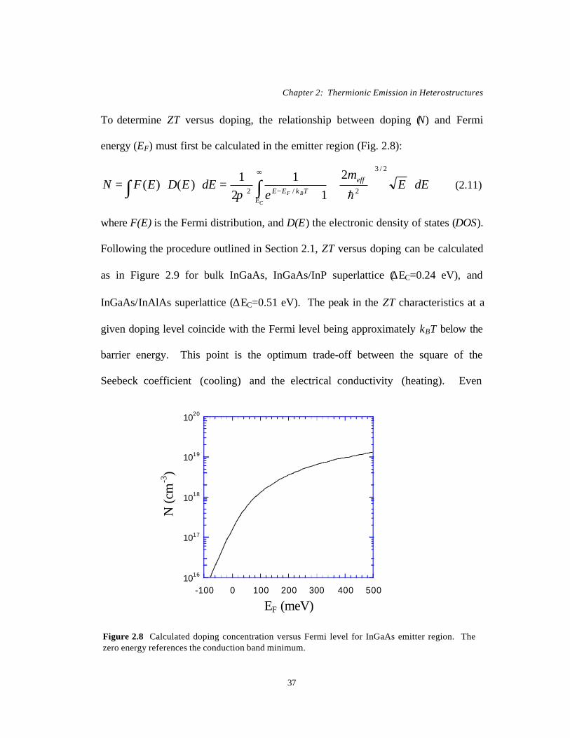
Chapter 2: Thermionic Emission in Heterostructures
37
To determine ZT versus doping, the relationship between doping (N) and Fermi
energy (EF) must first be calculated in the emitter region (Fig. 2.8):
where F(E) is the Fermi distribution, and D(E) the electronic density of states (DOS).
Following the procedure outlined in Section 2.1, ZT versus doping can be calculated
as in Figure 2.9 for bulk InGaAs, InGaAs/InP superlattice (∆EC=0.24 eV), and
InGaAs/InAlAs superlattice (∆EC=0.51 eV). The peak in the ZT characteristics at a
given doping level coincide with the Fermi level being approximately kBT below the
barrier energy. This point is the optimum trade-off between the square of the
Seebeck coefficient (cooling) and the electrical conductivity (heating). Even
∫∫∞
−⋅
⋅
+=⋅⋅=
C
BFE
effTkEE
dEEm
edEEDEFN
2/3
2/2
2
11
21)()(
hπ(2.11)
1016
1017
1018
1019
1020
-100 0 100 200 300 400 500
EF (meV)
N (c
m-3
)
Figure 2.8 Calculated doping concentration versus Fermi level for InGaAs emitter region. Thezero energy references the conduction band minimum.

Chapter 2: Thermionic Emission in Heterostructures
38
considering the reduction in mobility at the higher dopant concentrations (this was
experimentally measured and included in the calculation), the InGaAs/InAlAs
superlattice shows close to an order of magnitude improvement in the overall ZT
compared to the bulk InGaAs value. However, the design of these high barrier
0
0.05
0.1
0.15
0.2
0.25
0.3
0.35
1017 1018 1019 1020
N (cm-3)
ZT
Figure 2.9 Schematic and calculated ZT for bulk InGaAs and for high barrier heterostructurethermionic coolers based on InGaAs/InP (∆EC=0.24eV) and InGaAs/InAlAs (∆EC=0.51eV) atvarious doping densities. The peak in the ZT characteristic at a given doping correspondsapproximately to the Fermi level being ~ kBT below the barrier. The thermal conductivity of thecomposite material is taken to be 5 W/mK.
Bulk InGaAs
InGaAs/InP
InGaAs/InAlAs
DOS
Fermi Energy
~ kBT
BarrierHeight >> kBT
Ener
gy
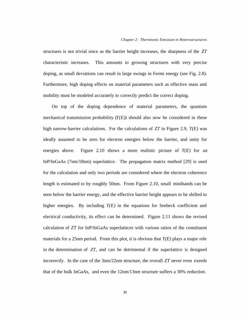
Chapter 2: Thermionic Emission in Heterostructures
39
structures is not trivial since as the barrier height increases, the sharpness of the ZT
characteristic increases. This amounts to growing structures with very precise
doping, as small deviations can result in large swings in Fermi energy (see Fig. 2.8).
Furthermore, high doping effects on material parameters such as effective mass and
mobility must be modeled accurately to correctly predict the correct doping.
On top of the doping dependence of material parameters, the quantum
mechanical transmission probability (T(E)) should also now be considered in these
high narrow-barrier calculations. For the calculations of ZT in Figure 2.9, T(E) was
ideally assumed to be zero for electron energies below the barrier, and unity for
energies above. Figure 2.10 shows a more realistic picture of T(E) for an
InP/InGaAs (7nm/18nm) superlattice. The propagation matrix method [29] is used
for the calculation and only two periods are considered where the electron coherence
length is estimated to by roughly 50nm. From Figure 2.10, small minibands can be
seen below the barrier energy, and the effective barrier height appears to be shifted to
higher energies. By including T(E) in the equations for Seebeck coefficient and
electrical conductivity, its effect can be determined. Figure 2.11 shows the revised
calculation of ZT for InP/InGaAs superlattices with various ratios of the constituent
materials for a 25nm period. From this plot, it is obvious that T(E) plays a major role
in the determination of ZT, and can be detrimental if the superlattice is designed
incorrectly. In the case of the 3nm/22nm structure, the overall ZT never even exeeds
that of the bulk InGaAs, and even the 12nm/13nm structure suffers a 30% reduction.

Chapter 2: Thermionic Emission in Heterostructures
40
0
0.2
0.4
0.6
0.8
1
0 0.2 0.4 0.6 0.8 1Energy (eV)
Tran
smis
sion
Pro
babi
lity
Figure 2.10 Quantum mechanical transmission probability versus energy for two periods of7nm/18nm InP/InGaAs superlattice. The dashed line indicates the barrier height of 0.24 eV wherethe zero on the energy scale corresponds to the minimum conduction band energy in the InGaAsemitter region.
0
0.05
0.1
0.15
0.2
2 1018 4 1018 6 1018 8 1018 1 1019
3/227/1812/13ideal
N (cm-3)
ZT
Figure 2.11 Calculation of ZT for InP/InGaAs superlattices with various ratios of the constituentmaterials for a 25nm period where the quantum mechanical transmission probability is considered.In the ideal case the period is irrelevant, and the transmission probability is assumed to be zero forenergies below the barrier and unity for energies above. Significant decreases can be seen in ZTdue to miniband conduction.

Chapter 2: Thermionic Emission in Heterostructures
41
For the 12nm/13nm ratio, a more accurate calculation would consider the 2D DOS in
the wells.
Interestingly, with careful design of the superlattice transport, the miniband
conduction can be tailored to provide cooling behavior of opposite polarity. If the
miniband window is made wide enough in energy and the Fermi energy is placed
Figure 2.12 Calculated Seebeck coefficient and electrical conductivity for three periods of3nm/5nm InAlAs/InGaAs. The Seebeck coefficient changes sign for certain doping levels. Thesimplified diagram above illustrates the concept of manipulating the miniband conduction forelectron filtering.
N (cm-3)
σ (Ω-1m
-1)S (V
/K)
-400 10-6
-200 10-6
0 100
200 10-6
400 10-6
600 10-6
0 100
100 103
200 103
300 103
400 103
1017 1018 1019 1020
miniband~ kBT
EC
EF
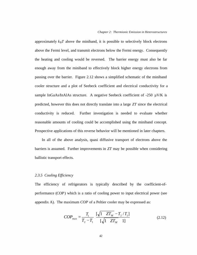
Chapter 2: Thermionic Emission in Heterostructures
42
approximately kBT above the miniband, it is possible to selectively block electrons
above the Fermi level, and transmit electrons below the Fermi energy. Consequently
the heating and cooling would be reversed. The barrier energy must also be far
enough away from the miniband to effectively block higher energy electrons from
passing over the barrier. Figure 2.12 shows a simplified schematic of the miniband
cooler structure and a plot of Seebeck coefficient and electrical conductivity for a
sample InGaAs/InAlAs structure. A negative Seebeck coefficient of -250 µV/K is
predicted, however this does not directly translate into a large ZT since the electrical
conductivity is reduced. Further investigation is needed to evaluate whether
reasonable amounts of cooling could be accomplished using the miniband concept.
Prospective applications of this reverse behavior will be mentioned in later chapters.
In all of the above analysis, quasi diffusive transport of electrons above the
barriers is assumed. Further improvements in ZT may be possible when considering
ballistic transport effects.
2.3.5 Cooling Efficiency
The efficiency of refrigerators is typically described by the coefficient-of-
performance (COP ) which is a ratio of cooling power to input electrical power (see
appendix A). The maximum COP of a Peltier cooler may be expressed as:
]11[
]/1[ 12
12
1max ++
−+⋅
−=
M
M
ZT
TTZTTT
TCOP (2.12)

Chapter 2: Thermionic Emission in Heterostructures
43
where T1 is the source temperature, T2 is the sink temperature, and TM is the mean
temperature [4]. Taking the best ZT of 0.31 from Figure 2.9, the efficiency of the
InGaAs/InAlAs heterostructure thermionic cooler is only about 7% of the ideal
thermodynamic COP. Fortunately in optoelectronic cooling applications, efficiency
is not of critical importance, and the devices need only provide the required amount
of cooling power. It is possible however to further increase the efficiency of the
coolers. The main problem is that the high cooling power at the cathode needs to
fight the large heat flux that is coming from the hot junction only a few microns
away. The concepts of using thicker films or minimizing thermal conductivity in
superlattices from the previous sections would contribute significantly to improving
the efficiency. More generally speaking, any increase in ZT will improve the
efficiency.
2.4 Cascading Coolers for Larger ∆T
Considering that a single thin barrier can provide such a significant amount of
cooling, an obvious question to ask is whether cascading coolers is possible to
achieve even greater temperature differentials. Theoretically it should be possible to
achieve any temperature down to absolute zero, however practical limitations
prevent this in reality. One of the problems that arise is in the lower stages having to
pump the ever increasing amount of heat that is passed on by the upper stages. This
argument explains why conventional multistage thermoelectric coolers are limited in
Chapter 2: Thermionic Emission in Heterostructures
44
the number of stages they use. This is also why there are always more
thermoelements in the lower stages than the upper stages. A similar concept would
need to be applied to a multistage heterostructure thermionic cooler.
Other, more physical challenges lie in the realization of such stacked structures.
A continuous growth of several stages of thermionic coolers becomes exceedingly
difficult as the number of stages increases. The only alternative is to take separate
stages and join them mechanically by fusion or some other bonding technique, but
this is also limited in the tolerance of the device to continuing processing steps. It is
not known at this time as to the practical limits on the number of stages for cascading
thermionic coolers, but conventional TE coolers are rarely ever more than eight
stages.
2.5 Summary
In the beginning of this chapter, a clear explanation of the microscopic origin of
Peltier cooling was presented. Using this basis, thermionic emission cooling in
heterostructures was proposed as a way to improve upon the bulk-material cooling
properties. While the concepts that were discussed are applicable to many material
systems, the InP-based system was used to illustrate more quantitatively the theory
involved. A general set of guidelines for the design of such coolers was presented,
and the main considerations discussed. It was shown that large enhancements in the
figure of merit, ZT, can be achieved using thermionic emission in heterostructures,

Chapter 2: Thermionic Emission in Heterostructures
45
especially for high barrier devices which showed an order of magnitude
improvement with InAlAs heterobarriers. Furthermore, it was shown for the first
time that the use of miniband conduction in superlattices makes possible the design
of n-type structures that exhibit p-type cooling behavior.
REFERENCES
1. G.D. Mahan, “Thermionic refrigeration,” Journal of Applied Physics, Vol. 76, No.7, 1 Oct. 1994,p. 4362-6.
2. A. Shakouri, E.Y. Lee, D.L. Smith, V. Narayanamurti, J.E. Bowers, “Thermoelectric effects insubmicron heterostructure barriers,” Microscale Thermophysical Engineering, Vol 2, No. 37,1998.
3. H.J. Goldsmid, Electronic Refrigeration. London: Pion Limited, 1986.
4. D.M. Rowe, CRC Handbook of Thermoelectrics. New York: CRC Press, 1995.
5. D.M. Rowe, C.M. Bhandari, Modern Thermoelectrics. Reston, Virgina: Reston Publishing Co.,1983.
6. L.D. Hicks, M.S. Dresselhaus, “Effect of Quantum-Well Structures on the Thermoelectric Figureof Merit,” Physical Review B, Vol. 47, 1993, p. 12727-31.
7. T.C. Harman, D.L. Spears, M.J. Manfra, “High Thermoelectric Figures of Merit in PbTeQuantum Wells,” J. Electron. Mater., Vol 25, 1996, p.1121-7.
8. J.O. Sofo, G.D. Mahan, “Thermoelectric Figure of Merit of Superlattices,” Applied PhysicsLetters, Vol. 65, 1994, p.2690-2.
9. D.A. Broido, T.L. Reinecke, “Thermoelectric Transport in Quantum Well Superlattices,” AppliedPhysics Letters, Vol. 70, 1997, p.2834-6.
10. D.M. Rowe, G. Min, “Multiple potential barriers as a possible mechanism to increase the Seebeckcoefficient and electrical power factor,” Proceedings of the 13th International Conference onThermoelectrics, Kansas City, 1994, p. 339-42.
11. L.W. Whitlow, T. Hirano, “Superlattice applications to thermoelectricity,” Journal of AppliedPhysics, Vol. 78, 1995, p. 5460-6.

Chapter 2: Thermionic Emission in Heterostructures
46
12. B. Moyzhes, “Possible ways for efficiency improvement of thermoelectric materials,”Proceedings of the 15th International Conference on Thermoelectrics, Pasadena, CA, 1996,p.183-7.
13. G.D. Mahan, “Figure of merit for thermoelectrics,” Journal of Applied Physics, Vol. 65, 1989,p.1578-83.
14. J.O. Sofo, G.D. Mahan, “Optimum band gap of a thermoelectric material,” Physical Review B,Vol. 49, 1994, p.4565-70.
15. D.A. Broido, T.L. Reinecke, “Effect of Superlattice Structure on the Thermoelectric Figure ofMerit,” Physical Review B, Vol. 51, 1995, p.13797-13800.
16. A. Shakouri, J. E. Bowers, “Heterostructure integrated thermionic coolers,” Applied PhysicsLetters, Vol.71, No.9, 1 September 1997, p. 1234-6.
17. A. Shakouri, J.E. Bowers, “Heterostructure Integrated Thermionic Refrigeration,” Internationalconference on Thermoelectrics, Dresden, Germany, Aug.26-29, 1997.
18. A. Shakouri, C.J. LaBounty, P. Abraham, J. Piprek, and J.E. Bowers, “Enhanced thermionicemission cooling in high barrier superlattice heterostructures,” Mat. Res. Soc. Symp. Proc., Vol.545, Dec. 1998, p.449-458.
19. A. Shakouri, C.J. LaBounty, J. Piprek, P. Abraham, and J.E. Bowers, “Thermionic emissioncooling in single barrier heterostructures,” Applied Physics Letters, Vol. 74, No.1, Jan. 1999,p.88-89.
20. B. Moyzhes, V. Nemchinsky, “Thermoelectric figure of merit of metal-semiconductor barrierstructure based on energy relaxation length,” Applied Physics Letters, Vol. 73, 1998, p.1895-7.
21. G.D. Mahan, L.M. Woods, “Multilayer thermionic refrigeration,” Phys. Rev. Lett., Vol. 80, 1998,p.4016.
22. S.M. Sze, Physics of Semiconductor Devices. New York: Wiley, 1981.
23. G. Stareev, H. Kunzel, G. Dortmann, “A controllable mechanism of forming extremely low-resistance nonalloyed ohmic contacts to group III-V compound semiconductors,” Journal ofApplied Physics, Vol. 74, No.12, 15 Dec. 1993, p.7344-55.
24. P. Hyldgaard, G.D. Mahan, “Phonon superlattice transport,” Physical Review B, Vol. 56, No.17,1 Nov. 1997, p.10754-7.
25. G. Chen, “Thermal conductivity and ballistic-phonon transport in the cross-plane direction ofsuperlattices,” Physical Review B, Vol. 57, No.23, 15 June 1998, p.14958-73.
26. V. Narayanamurti, H.L. Stormer, M.A. Chin, A.C. Gossard, W. Wiegmann, “SelectiveTransmission of High-Frequency Phonons by a Superlattice: The “Dielectric” Phonon Filter,”Physical Review Letters, Vol. 43, 1979, p.2012-2016.
Chapter 2: Thermionic Emission in Heterostructures
47
27. R. Venkatasubramanian, “Lattice thermal conductivity reduction and phonon localizationbehavior in superlattice structures,” Physical Review B, Vol. 61, No.4, 15 Jan. 2000, p.3091-7.
28. C. Kittel, Introduction to Solid State Physics. New York: Wiley, 1996.
29. H. Kroemer, Quantum Mechanics: For Engineering, Materials Science, and Applied Physics.New Jersey: Prentice-Hall, 1994.

Chapter 2: Thermionic Emission in Heterostructures
48

Chapter 3: Heterostructure Design and Growth
48
Chapter 3
Heterostructure Design and Growth
In Chapter 2, it was shown that for certain approximations, thermionics and
thermoelectrics have the same material figure-of-merit. As discussed below, the use
of high barrier thermionic emission coolers relaxes the need for high effective mass.
Considering this, many III-V compounds used in optoelectronic devices actually
have very attractive cooling properties. Several proposed structures will be
described and investigated in this chapter, all of which were grown lattice matched to
InP substrates. The experimentally measured material properties of the grown
structures will be discussed more fully in Chapter 4.
3.1 Thermoelectric and Thermionic Material Figure-of-Merit
To review, the material figure-of-merit of thermoelectrics and low-barrier
thermionics can be expressed as µ(m*)1.5/β , where µ is the mobility, m* the effective
mass, and β the thermal conductivity. Figure 3.1a shows this material figure-of-
merit for several different semiconductor systems. SiGe is already an important
thermoelectric material for high temperatures (>900°C), and is an attractive material
for thermionic cooling at room temperature [1,2]. Bi2Te3, the dominant
thermoelectric material at room temperature, is also a good candidate for thermionic
cooling, but the crystal growth and processing technology is not as mature as SiGe

Chapter 3: Heterostructure Design and Growth
49
[3]. Other materials such as InGaAs and HgCdTe are well suited for integration with
optoelectronic devices and infrared detectors respectively. While these latter two
material systems have a material figure-of-merit that is roughly an order of
magnitude smaller, a fundamental feature of thermionic cooling in heterostructures is
the reduced constraints on material choice. Specifically, thermionic cooling relaxes
the requirement for high thermopower since the band edge discontinuities perform
the work of creating large asymmetries in the transport energy. This equates to
negating the requirement for large effective mass in the material figure-of-merit
expression. The need for large effective mass stems from the curvature of the energy
versus momentum relation relating the need for large asymmetry in the density-of-
states. Therefore, the barrier material should simply have an adequate electrical
conductivity and a low thermal conductivity making ternaries and quartenaries good
candidates for barrier elements. Figure 3.1b shows the ratio of µ/β with the effective
mass term eliminated. Many of the III-V semiconductor compounds now appear to
have a larger figure-of-merit than even Bi2Te3.
To go step further, the restraint on thermal conductivity could also be alleviated
if the hot electrons arriving at the anode could lose their energy by photon emission
instead of passing their energy to the lattice as heat. This concept of integrating light
emitting structures was previously proposed by Shakouri et al. [4]. In this
configuration, a high thermally conducting barrier material, such as InP, would be
beneficial.

Chapter 3: Heterostructure Design and Growth
50
0.0001
0.001
0.01
0.1
1
AlS
bG
aAs
GaN
GaP
GaS
bH
gC
dT
e .2
Hg
Cd
Te
.3H
gC
dT
e .4
Hg
Cd
Te
.5H
gC
dT
e .6
Hg
Cd
Te
.7In
As
InG
aAs
.53
InG
aAsP
.77,
.5 InN
InP
InS
bG
e (n
)G
e (p
)S
i (n
)S
i (p
)S
iGe
.7 (
n)S
iGe
.7 (
p)B
iTe
(n c
) (n)
BiT
e (n
c) (
p)
10-5
0.0001
0.001
0.01
0.1
AlP
AlS
bG
aAs
GaN
GaP
GaS
bH
gCdT
e .2
HgC
dTe
.3H
gCdT
e .4
HgC
dTe
.5H
gCdT
e .6
HgC
dTe
.7In
As
InG
aAs
.53
InG
aAsP
.77,
.5 InN
InP
InS
bG
e (n
)G
e (p
)S
i (n
)S
i (p
)S
iGe
.7 (n
)S
iGe
.7 (p
)B
iTe
(n c
) (n
)B
iTe
(n c
) (p
)
Figure 3.1 (a) The material parameter µ(m*)1.5/β for different compounds indicates the prospectsof various semiconductors for low-barrier thermionic or thermoelectric cooling. µ is the mobility inthe barrier layer, β is the thermal conductivity, and m* is the carrier effective mass. (b) Themodified material parameter neglecting the effective mass.
µ(m
*)1.
5 /β(a)
(b)
µ/β
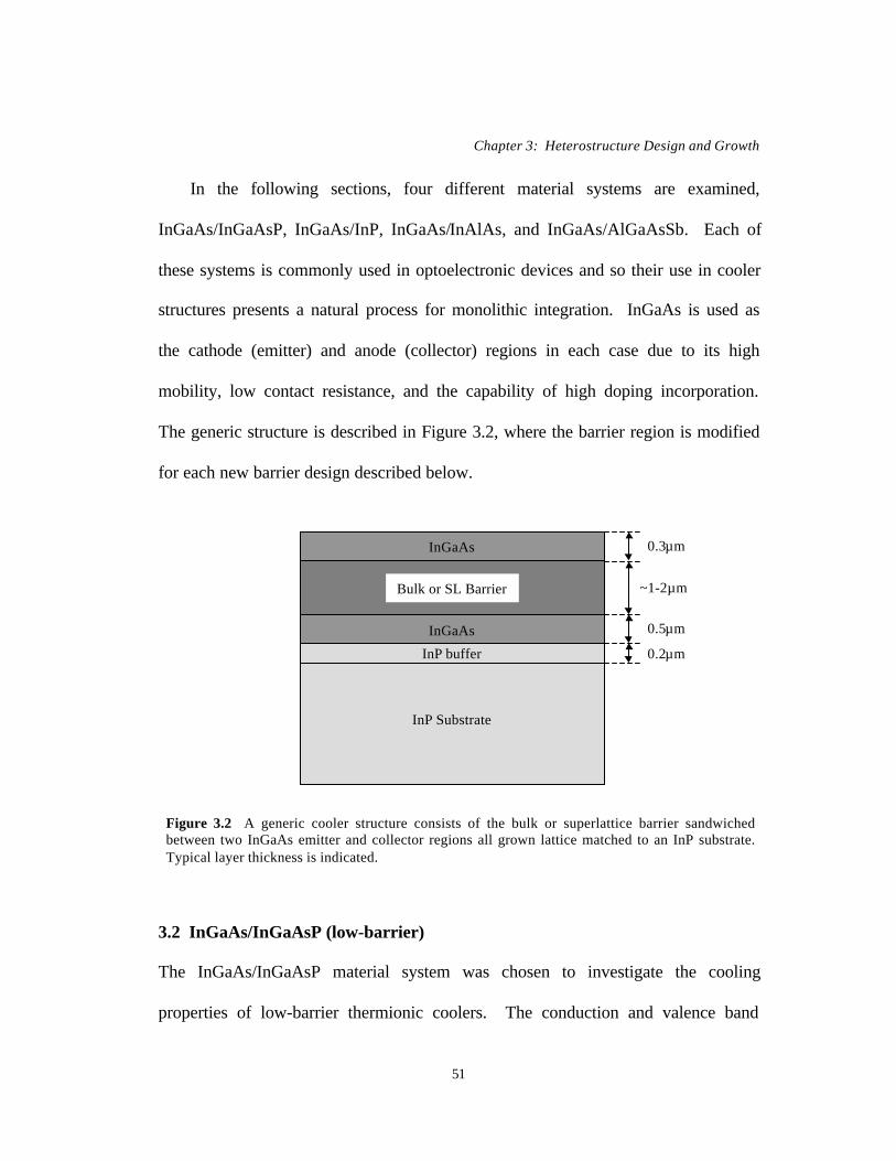
Chapter 3: Heterostructure Design and Growth
51
In the following sections, four different material systems are examined,
InGaAs/InGaAsP, InGaAs/InP, InGaAs/InAlAs, and InGaAs/AlGaAsSb. Each of
these systems is commonly used in optoelectronic devices and so their use in cooler
structures presents a natural process for monolithic integration. InGaAs is used as
the cathode (emitter) and anode (collector) regions in each case due to its high
mobility, low contact resistance, and the capability of high doping incorporation.
The generic structure is described in Figure 3.2, where the barrier region is modified
for each new barrier design described below.
3.2 InGaAs/InGaAsP (low-barrier)
The InGaAs/InGaAsP material system was chosen to investigate the cooling
properties of low-barrier thermionic coolers. The conduction and valence band
InP Substrate
InP buffer
InGaAs
InGaAs
Bulk or SL Barrier
0.2µm
0.5µm
~1-2µm
0.3µm
Figure 3.2 A generic cooler structure consists of the bulk or superlattice barrier sandwichedbetween two InGaAs emitter and collector regions all grown lattice matched to an InP substrate.Typical layer thickness is indicated.

Chapter 3: Heterostructure Design and Growth
52
offsets are 110 meV and 102 meV respectively, when lattice matched to InP
(InGaAsP λgap=1.3µm) [5,6]. The nearly equal offsets in both the conduction and
valence bands allow for suitable barriers in both n- and p-type structures. Metal
organic chemical vapor deposition (MOCVD) was used to grow bulk and
superlattice samples, and all compositions were grown lattice matched to the InP
growth substrate. The substrates used for cooling were highly doped to reduce any
additional Joule heating in the substrates, while additional growths were done on
semi-insulating substrates for material characterization.
While many variations in growth were investigated, the typical n-type device
consisted of a 25 period superlattice of 10nm InGaAs and 30nm InGaAsP, giving a
total thickness of 1µm. The doping was chosen so that the Fermi level was optimally
located approximately kBT below the barrier as discussed in Chapter 2. A one-
dimensional semiconductor device simulator [7] was used to calculate the band
diagram and Fermi level as shown in Figure 3.3 under equilibrium. A doping of
3×1018 cm-3 was used in the InGaAs regions while the InGaAsP regions were
undoped. Figure 3.4 shows the simulated current versus voltage for this structure.
The current remains in a linear regime below 105 A/cm2.
The p-type material was grown with a 67 period superlattice of 10nm InGaAs
and 5nm InGaAsP, also giving a total thickness of 1 µm. The quartenary is kept
shorter in the p-type structure due to the lower mobility compared to n-type material.
The optimum doping was found to be much higher for the p-type barrier due to the

Chapter 3: Heterostructure Design and Growth
53
-0.05
0
0.05
0.1
0.15
0 0.2 0.4 0.6 0.8 1 1.2
Position (µm)
Ene
rgy
(eV
)
Figure 3.3 Simulated conduction band diagram and Fermi level at equilibrium for a 10nm/40nmInGaAs/InGaAsP (λgap=1.3µm) superlattice barrier with InGaAs emitter and collector regions. TheInGaAs regions are doped to 3×1018 cm-3 and the InGaAsP regions are undoped. All compositionsare lattice matched to InP.
EC
EF
0
1 105
2 105
3 105
0 1 2 3 4
V (V)
J (A
/cm
2 )
Figure 3.4 Simulated current-voltage relationship for the structure shown in Figure 3.3. Thecurrent is linearly dependent on voltage below 105 A/cm2.

Chapter 3: Heterostructure Design and Growth
54
increased density-of-states. A value of 1×1019 cm-3 was used in the InGaAs regions,
and a slightly lower value in the InGaAsP barriers.
3.3 InGaAs/InP (high-barrier)
The advantages of high-barrier InGaAs/InP structures were previously mentioned in
the ZT calculations of Chapter 2. Due to the larger band offsets in this material
system (∆Eg=0.75eV), only n-type materials are considered since the doping levels
required for p-type material (>2×1019 cm-3) are not readily available. The conduction
band offset used here and in the previous calculations is 0.242 eV [5]. A variety of
structures were grown to study cooling for different superlattices in an attempt to
optimize the design parameters. The InP barriers were undoped while doping in the
InGaAs regions was varied in an attempt to optimize the Fermi level, and ranged
from 5×10¹⁷ to 9×1018 cm-3. The InGaAs/InP superlattice period was also modified
between 22nm/3nm and 18nm/7nm. Barrier thickness was typically 2 µm, but
several superlattices were grown as thick as 6 µm.
As the current bias is increased, the effective difference in energy between the
quasi-Fermi level and barrier (∆φ) is diminished [8]. While this effect could be
neglected in the low-barrier design, it is more pronounced in the high-barrier
superlattice and should be considered when attempting to optimize the Fermi level
with respect to the barrier edge. Ideally, the Fermi level is positioned approximately
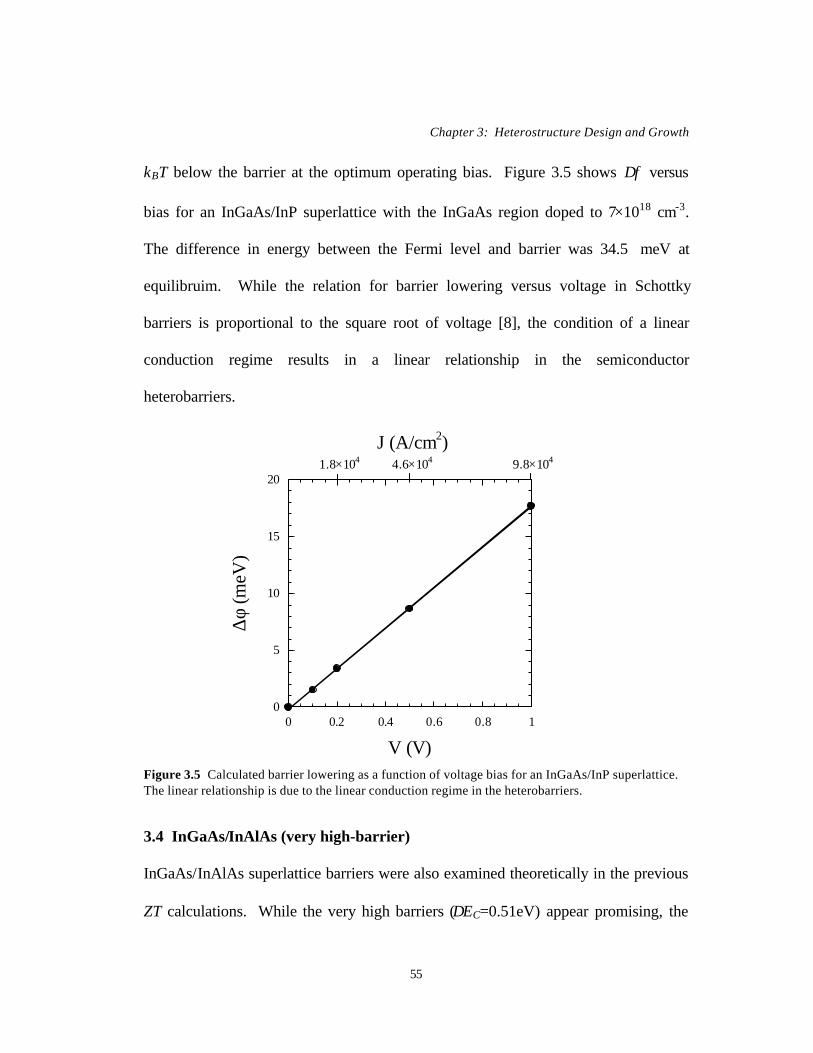
Chapter 3: Heterostructure Design and Growth
55
kBT below the barrier at the optimum operating bias. Figure 3.5 shows ∆φ versus
bias for an InGaAs/InP superlattice with the InGaAs region doped to 7×1018 cm-3.
The difference in energy between the Fermi level and barrier was 34.5 meV at
equilibruim. While the relation for barrier lowering versus voltage in Schottky
barriers is proportional to the square root of voltage [8], the condition of a linear
conduction regime results in a linear relationship in the semiconductor
heterobarriers.
3.4 InGaAs/InAlAs (very high-barrier)
InGaAs/InAlAs superlattice barriers were also examined theoretically in the previous
ZT calculations. While the very high barriers (∆EC=0.51eV) appear promising, the
0
5
10
15
20
0 0.2 0.4 0.6 0.8 1
V (V)
∆φ
(meV
)
Figure 3.5 Calculated barrier lowering as a function of voltage bias for an InGaAs/InP superlattice.The linear relationship is due to the linear conduction regime in the heterobarriers.
1.8×10⁴ 4.6×10⁴ 9.8×10⁴
J (A/cm2)

Chapter 3: Heterostructure Design and Growth
56
difficulty in designing and growing the structures presents a significant challenge.
From simply a design perspective, the predicted ZT is highly dependent on a number
of different assumed material constants and properties which are used in the
calculation of many factors such as transmission probability, density-of-states, and
Fermi level. Moreover, the growth of such highly modulation-doped structures
requires special techniques, and careful characterization is needed. Deviations about
the correct doping profile or layer thickness can have a large impact on the final
performance.
Several structures were attempted in this material system. Three micron thick
superlattices were composed of 120 periods of 20nm/5nm or 18nm/7nm
InGaAs/InAlAs. The wells were doped from 1.5×1019 cm-3 to 3.0×1019 cm-3 while
the barriers were non-intentionally-doped (nid).
3.5 InGaAs/AlGaAsSb
The InGaAs/AlGaAsSb material system has been investigated recently for the
development of distributed Bragg reflectors (DBR’s) for use in long-wavelength
vertical-cavity surface-emitting lasers (VCSEL’s) [9]. The foremost challenge for
the design of such devices is the low thermal conductivity of the Sb-based quartenary
material. This low thermal conductivity along with the relatively high Seebeck
coefficient make this material system very attractive for the development of
thermionic emission coolers and for integration with VCSEL’s. Furthermore, the
Chapter 3: Heterostructure Design and Growth
57
conduction band offsets can be tailored over a wide range by changing the Al and Sb
mole fractions [10].
A 2µm thick superlattice was grown, composed of 100 periods of 10nm/10nm
Al0.1GaAsSb/Al0.2GaAsSb sandwiched between InGaAs emitter and collector
regions. The superlattice was doped uniformly to 1018 cm-3 while the InGaAs
regions were doped to 5×1018 cm-3.
3.6 Summary
After reviewing the material figure-of-merit for thermoelectrics, it was explained that
thermionic emission in heterostructures relaxes the need for high thermopower (large
m*) in the material structure. With this in mind, it was shown that InP-based
material systems are favorable for the design of thermionic coolers due to the high
mobilities and low thermal conductivities. Four material systems were proposed for
experimental investigation of cooling: InGaAs/InGaAsP; InGaAs/InP;
InGaAs/InAlAs; and InGaAs/AlGaAsSb. The material properties of these structures
are discussed in Chapter 4.
REFERENCES
1. X. Fan, G. Zeng, C. LaBounty, E.Croke, A. Shakouri, C. Ahn, J.E. Bowers, “SiGeC/Sisuperlattice micro cooler,” Applied Physics Lett., Vol. 78, No.11, 12 March 2001, p. 1580-2.
2. X. Fan, G. Zeng, C. LaBounty, E. Croke, D. Vashaee, A. Shakouri, C. Ahn, J.E. Bowers, “Highcooling power density SiGe/Si micro coolers,” Elec. Lett., Vol. 37, No. 2, 18th January 2001,p.126-7.
Chapter 3: Heterostructure Design and Growth
58
3. L. Rushing , A. Shakouri, P. Abraham, J.E. Bowers, “Micro thermoelectric coolers for integratedapplications,” Proceedings of the 16th International Conference on Thermoelectrics, Dresden,Germany, August 1997, p. 646-9.
4. A. Shakouri, J.E. Bowers, “Heterostructure Integrated Thermionic Refrigeration,” Proceedingsof the 16th International Conference on Thermoelectrics, Dresden, Germany, August 1997, p.636-40.
5. P. Bhattacharya, Properties of Lattice-Matched and Strained Indium Gallium Arsenide. London:INSPEC, 1993.
6. E. Herbert Li, “Material parameters of InGaAsP and InAlGaAs systems for use in quantum wellstructures at low and room temperatures,” Physica E, Vol. 5, 2000, p. 215-73.
7. SimWindows Version 1.5.0 (1999) by D.W. Winston.
8. S.M. Sze, Physics of Semiconductor Devices. New York: Wiley, 1981.
9. G. Almuneau, E. Hall, T. Mukaihara, S. Nakagawa, C. Luo, D.R. Clarke, L.A. Coldren,“Improved Electrical and Thermal Properties of InP/AlGaAsSb Bragg Mirrors for Long-Wavelength Vertical Cavity Lasers,” IEEE Photon. Tech. Lett., Vol.12, No.10, 2000, p.1322-4.
10. A.F.M. Anwar, R.T. Webster, “Energy Bandgap of AlxGa1-xAs1-ySby and Conduction BandDiscontinuity of AlxGa1-xAs1-ySby/InAs and AlxGa1-xAs1-ySby/InGaAs Heterostructures,” Solid-State Electronics, Vol.42, No.11, 1998, p.2101-4.

Chapter 3: Heterostructure Design and Growth
59

Chapter 4: Material Characterization
61
Chapter 4
Material Characterization
The material properties of interest should be clear from our previous discussion of
ZT and the material figure-of-merit. Specifically, the electrical conductivity σ,
Seebeck coefficient S, and thermal conductivity β are of utmost concern. In many
cases conventional measurement techniques, as in Hall measurements for carrier
mobility, can be used to extract properties of interest. In other instances, new
methods must be developed to measure parameters such as the Seebeck coefficient
perpendicular to superlattice structures. For each of the material properties of
interest discussed below, the measurement methods are explained and the results
reviewed.
4.1 Electrical Conductivity
The importance of large electrical conductivity follows from minimizing Joule heat.
However, the trade-off between σ and S was shown explicitly in Chapter 2 when
trying to maximize the power factor S2σ. On that account, when qualifying a new
thermionic cooler structure, the electrical conductivity must be resolved. The
measurements described below are for in-plane transport. Cross-plane
measurements of conductivity and mobility are difficult to extract due to the small

Chapter 4: Material Characterization
62
dimensions and variable effects of current spreading, though methods have been
proposed based on a transmission line model [1].
The electrical conductivity can simply be measured through a resistivity
measurement (σ=1/ρ), however more insight is preferred into its contributions. The
electrical conductivity can be expressed as:
where q is the electron charge, n the carrier concentration, and µ the carrier mobility.
The carrier concentration and charge type (n-type or p-type) can be determined from
a Hall measurement [2]. Knowing the conductivity and carrier concentration, the
mobility can then be deduced. The mobility for a given doping concentration gives a
measure of material quality and the quality of superlattice interfaces where carrier
scattering may occur.
4.1.1 Experimental Results
Figure 4.1 shows experimentally measured values for bulk n- and p-type
materials, as well as various n-type superlattice systems. The most obvious
distinction is between the n- and p-type mobility. This is largely due to the order of
magnitude difference in effective mass for holes and electrons since mobility is
inversely proportional to effective mass. For example, the electron effective mass in
InGaAs is 0.041mo while the hole effective mass is 0.46mo. Fortunately, the low
mobility, and consequently low conductivity, can be offset with higher doping and
µσ qn= (4.1)

Chapter 4: Material Characterization
63
Figure 4.1 Mobility versus doping for various (a) n-type materials, (b) p-type materials, and (c) n-type superlattice systems. The InP values are referenced experimental values from INSPEC [3].All other values were experimentally measured by the Hall effect.
01000
2000
30004000
5000
60007000
1017 1018 1019 1020
Doping (cm-3)
µ (c
m2 /V
s) InGaAs (n)
InP (n)
InGaAsP (n)
(a)
Doping (cm-3)
µ (c
m2 /V
s)
20
40
60
80
100
120
140
1017 1018 1019 1020
(b)
InP (p) InGaAs (p)
1000
2000
3000
4000
5000
6000
1017 1018 1019 1020
(c)
Doping (cm-3)
µ (c
m2 /V
s)
InGaAs/InP (n)
InGaAs/AlGaAsSb (n)
InGaAs/InGaAsP (n)
InGaAs/InAlAs (n)

Chapter 4: Material Characterization
64
the inherently larger Seebeck coefficient. For the superlattice systems, most of the
structures are modulation doped and the barrier regions are kept thin so the in-plane
transport is dominated by conduction in the InGaAs well regions. This explains the
close spacing of data points for all the superlattice structures. The overall electrical
conductivity is on the order of 1500 Ω-1cm-1 for n-type structures and 100 Ω-1cm-1
for p-type structures. These values are typically less than the corresponding contact
resistance in fabricated devices, and so are not limiting cooling performance.
4.2 Thermal Conductivity
Thermal conductivity is perhaps even more important than the electrical conductivity
as no other variation has a more direct impact on cooling. While other sources of
electrical resistance dominate over the material conductivity, the thermal
conductivity is considered a limiting factor in current device results. To this end, the
superlattice design continually seeks to minimize β . Several encouraging reports
have been made regarding reduced thermal conductivity with superlattices compared
to bulk values in III-V systems [4-7]. Generally, they indicate that short periods
produce the lowest thermal conductivity (< 50nm).
4.2.1 Experimental Results
Thermal conductivity perpendicular to the superlattice is of special interest for
heterostructure thermionic cooling since the majority of electrical and thermal
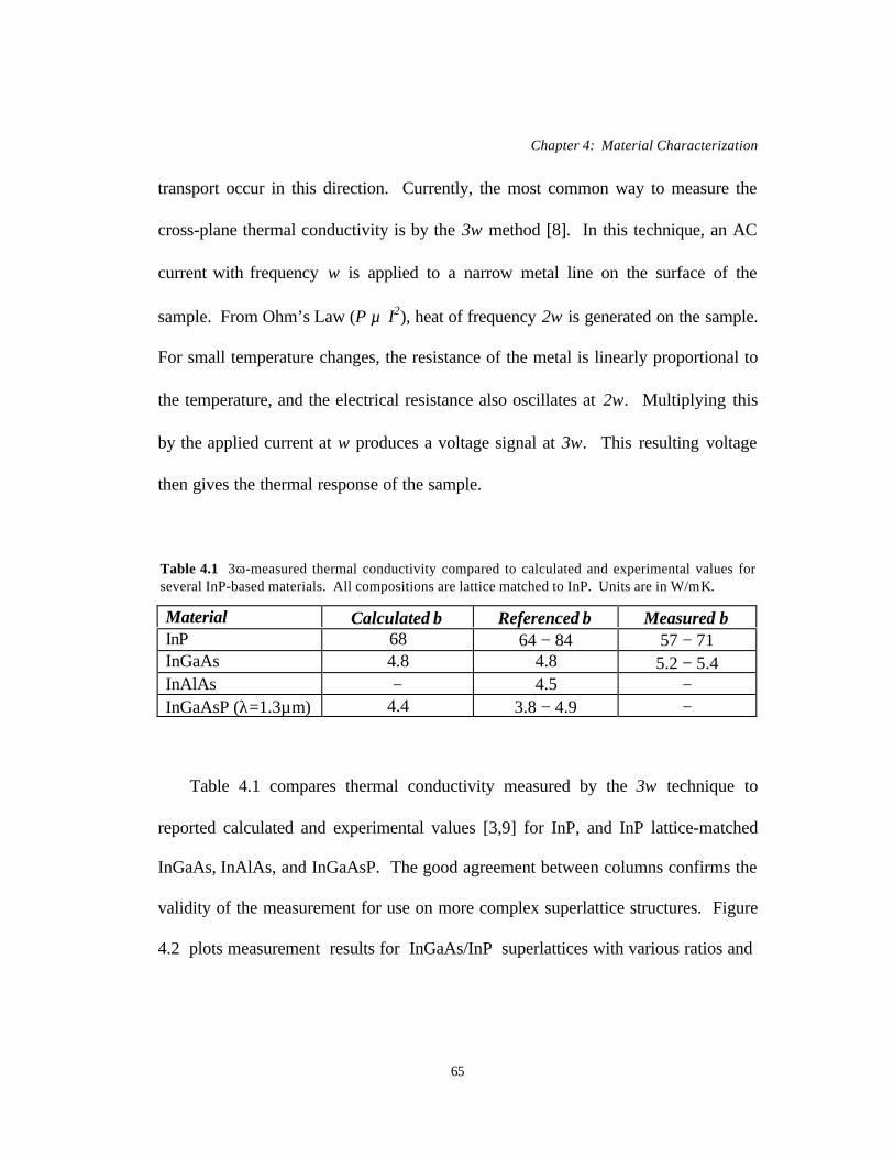
Chapter 4: Material Characterization
65
transport occur in this direction. Currently, the most common way to measure the
cross-plane thermal conductivity is by the 3ω method [8]. In this technique, an AC
current with frequency ω is applied to a narrow metal line on the surface of the
sample. From Ohm’s Law (P ∝ I2), heat of frequency 2ω is generated on the sample.
For small temperature changes, the resistance of the metal is linearly proportional to
the temperature, and the electrical resistance also oscillates at 2ω. Multiplying this
by the applied current at ω produces a voltage signal at 3ω. This resulting voltage
then gives the thermal response of the sample.
Material Calculated β Referenced β Measured βInP 68 64 − 84 57 − 71InGaAs 4.8 4.8 5.2 − 5.4InAlAs − 4.5 −InGaAsP (λ=1.3µm) 4.4 3.8 − 4.9 −
Table 4.1 compares thermal conductivity measured by the 3ω technique to
reported calculated and experimental values [3,9] for InP, and InP lattice-matched
InGaAs, InAlAs, and InGaAsP. The good agreement between columns confirms the
validity of the measurement for use on more complex superlattice structures. Figure
4.2 plots measurement results for InGaAs/InP superlattices with various ratios and
Table 4.1 3ω-measured thermal conductivity compared to calculated and experimental values forseveral InP-based materials. All compositions are lattice matched to InP. Units are in W/m⋅K.

Chapter 4: Material Characterization
66
constant period [10]. Looking simply at the bulk values of β , as the amount of InP is
increased, the effective thermal conductivity (βeff) is expected to increase as:
where d is the thickness of the corresponding material for a single period. This
average β is based on Fourier’s law of heat conduction, and does not take into
account effects such as interface scattering or phonon filtering. These other effects
are shown to be important however, as the measured values show βeff decreasing for
increasing InP, even though InP has an order of magnitude greater β than InGaAs.
InP
InP
InGaAs
InGaAs
eff
InPInGaAs ddddβββ
+=+
(4.2)
4
5
6
7
8
22/3
β (W
/m⋅K
)
Figure 4.2 Thermal conductivity versus the ratio of InGaAs/InP for a constant superlattice period.The circles are experimentally measured values while the squares were calculated geometricalaverages from experimental bulk values of the constituent materials. Opposite trends are observedeven though the same number of interfaces are present. Experimental values from S. Huxtable.
20/5
18/7
Superlattice Period (nm/nm)
Measured Average

Chapter 4: Material Characterization
67
Since the same number of interfaces are present in all cases, the result cannot be
explained by discrete-interface phonon-scattering effects, and must be due to some
other phonon transport physics.
Figure 4.3 summarizes the theoretical and experimental results for the
AlxGaAsSb system where all compositions are lattice matched to InP. The thermal
conductivity for the distributed Bragg reflectors (DBR’s) is quite low, suggesting
that the DBR’s themselves are potentially attractive materials for thermionic cooling.
The superlattice structure investigated for thermionic cooling is shown as a solid dot
in Figure 4.3, and was composed of 10nm/10nm Al0.1GaAsSb/Al0.2GaAsSb.
0
0.02
0.04
0.06
0.08
0.1
0 0.2 0.4 0.6 0.8 1
Al Composition x
β (W
/cm
⋅K)
Figure 4.3 Measured and theoretical thermal conductivity for various AlGaAsSb compounds and Alcompositions. The superlattice structure investigated for thermionic cooling was 10nm/10nmAl0.1GaAsSb/Al0.2GaAsSb. DBR values from G. Almuneau.
Al0.2GaAsSb/InP DBR Exp.
AlxGaAsSb Theory
Al0.2GaAsSbExp.
AlAsSbExp.Al0.2GaAsSb/AlAsSb
DBR Exp.
Al0.1GaAsSb/Al0.2GaAsSb Exp.

Chapter 4: Material Characterization
68
Overall, more than an order of magnitude difference in β between the InP-
substrate and other epitaxial films is evident. This bodes well for thermionic coolers
on InP substrates since the substrate needs to provide as ideal a heat sink as possible
for the thin film cooler.
4.3 Seebeck Coefficient
When considering superlattices, a distinction must be made between the in-plane and
cross-plane Seebeck coefficient. While enhancements can be seen in the in-plane
direction for lower-dimensional structures, the cross-plane properties are of more
interest for heterostructure thermionic cooling. Still, the in-plane measurement is
important for characterizing the bulk thermoelectric effect between the metal and
contact layers which is in addition to any thermionic emission cooling.
4.3.1 In-Plane
The in-plane and bulk Seebeck coefficient can both be measured in a similar manner.
By applying a temperature gradient across a sample and measuring the generated
voltage, the ratio of voltage/temperature determines the Seebeck coefficient. N- and
p-type substrates were measured, and Seebeck coefficients of 70 and 520 µV/K were
measured, respectively. The substrates were both doped to 5×1018 cm-3, the same as
all growth substrates for cooler samples.

Chapter 4: Material Characterization
69
4.3.2 Cross-Plane
A direct measurement of the cross-plane Seebeck coefficient is difficult at best.
Simply applying the same procedure as the in-plane case is not practical because of
the dimensions and geometry of the problem. Whereas before temperature and
voltage were measured across hundreds of microns, the same parameters need to be
measured across thin films on the order of a few microns. In addition, the bottom of
the film is not directly accessible, so temperature and voltage need to be inferred
from points on the surface. Clearly an alternate measurement method is needed.
The Harman method [11] and further refined transient method [12] have been
previously used to not only characterize the Seebeck coefficient, but also the overall
ZT in bulk thermoelectrics. These approaches are based on the inherent differences
in time response between the expected voltage from Ohm’s law (VR), and the
additional Seebeck voltage (VS). Figure 4.4 shows how these two components can be
resolved from the total device voltage VT, when a square current waveform is applied
to a commercial Peltier module with 62 thermoelements. Between the 60 second and
110 second time mark, the voltage has reached a steady state value. Looking closely
at the voltage at the 110 second mark, there is a nearly instantaneous ohmic voltage
drop due to the current turn-off. The remaining voltage is due to the Seebeck effect
which dies out exponentially due to the gradual temperature transient. In this
example, the measured Seebeck voltage was 100 mV and the temperature differential
was 7.88 K, giving a total Seebeck coefficient of 12.69 mV/K. This value can then

Chapter 4: Material Characterization
70
be divided by the total number of thermoelements in the module, resulting in a
material Seebeck coefficient of 205 µV/K, which is in good agreement with the
manufacturer specifications.
Time (s)
I (m
A)
0
50
100
150
200
250
0 50 100 150 200
(a)
Figure 4.4 (a) Applied current pulse and (b) resulting voltage waveform in the transient Seebeckmeasurement of a Peltier module. The total voltage VT is comprised of an instantaneous componentVR according to Ohm’s law, and an exponential component VS from the Seebeck voltage.
0
100
200
300
400
500
0 50 100 150 200
Time (s)
VT = VR + VS
VS = S⋅ (Th – Tc)VR = I⋅ R
V (m
V)
(b)

Chapter 4: Material Characterization
71
The application of this technique to single thermoelements is more difficult
however. The reason lies with the noise of the measured voltage signal. In the
analysis of the Peltier module, the Seebeck voltage of each element adds to produce
the measured voltage. For single elements, voltages on the order of micro-volts must
be resolved compared to milli-volts in the case of multi-element modules. Attempts
made with noise filters and low-noise amplifiers to extract the signal from single
element coolers have met little success.
Since measuring the cross-plane Seebeck coefficient has proven so difficult, an
alternative method was necessary to characterize the cooling potential. The cooling
potential for thermionic emission coolers is most associated with the barrier used to
filter charge carriers. The characterization of the barriers is discussed in the next
section.
4.4 Barrier Characterization
The entity responsible for modifying the cross-plane Seebeck coefficient is the
barrier used to create the necessary asymmetry in the charge carrier transport.
Characterizing the barrier can provide a way to compare various sample structures
when changing design variables such as doping, period, and materials. A
combination of low temperature current-voltage measurements and secondary ion
mass spectroscopy are used to determine the presence of barriers and estimate their
magnitudes.

Chapter 4: Material Characterization
72
4.4.1 Low Temperature I-V Characteristics
Using a liquid-helium cooled cryostat, current-voltage curves were measured for a
variety of superlattice designs. Figure 4.5 shows typical characteristics for a
10nm/30nm InGaAs/InGaAsP (1.5×1018cm-3/nid) superlattice with a device area of
100×100µm2. From room temperature to around 100 K, the I-V curves appear
linear. As the temperature is further reduced, the Fermi distribution narrows and less
carriers occupy the available states with energy greater than the barrier. Therefore,
at lower temperatures, the I-V curves become Schottky-like indicating that a barrier
is indeed present. Sample structures of metal contacts to InGaAs showed linear I-V
characteristics over the entire temperature range confirming that the Schottky effects
are not due to the metal-semiconductor junction. Figure 4.5b demonstrates how the
non- linearities change with increased doping in the InGaAs well regions. More
quantitative analysis of the I-V data is needed before an accurate correlation to
barrier height and Fermi level is possible.
Not all samples showed the observed behavior described above. In fact, the
majority of the InGaAs/InP and all the InGaAs/InAlAs samples showed completely
linear characteristics over the entire temperature range. The only explanation is that
the barrier is not present. This would suggest that the desired doping profile through
the structure is not as it should be.

Chapter 4: Material Characterization
73
Figure 4.5 (a) Current-voltage characteristics versus temperature for a 10nm/30nmInGaAs/InGaAsP (1.5×1018 cm-3/nid) superlattice. (b) Comparing the same structure for differentdoping levels. The device area was 100×100µm2. Measurement by D. Vashaee.
0
100
200
300
400
500
600
700
0 20 40 60 80 100
I (mA)
V (m
V)
(a)
320K120K
90K
70K
50K
20K4K
I (mA)
V (m
V)
(b)
0
100
200
300
400
500
600
700
0 20 40 60 80 100
4K5e18
4K1.5e18
70K1.5e18
70K5e18

Chapter 4: Material Characterization
74
4.4.2 SIMS Analysis
To further investigate the samples that did not indicate the presence of a barrier in
the low temperature I-V measurement, secondary ion mass spectrometry (SIMS) was
employed to analyze the atomic concentrations of the individual elements in the
MOCVD grown material. A sample SIMS result is shown in Figure 4.6 for a silicon-
doped 20nm/5nm InGaAs/InP superlattice. The superlattice structure can easily be
identified from the arsenic and phosphorus profiles. The feature of interest is the
silicon dopant profile that shows significant amounts and even peaks of silicon in the
barrier regions. Doping in the InP tends to drastically reduce the barrier, which
explains why the I-V curves were linear over all temperatures.
Incorporation of silicon doping in the barrier regions was believed to have
happened in one of two ways. Either a substantial amount of residual silicon was
present in the chamber after the shutter closed, during the InP growth, or the silicon
simply diffused during the growth. To solve the problem, a series of three test
structures were grown and analyzed again by SIMS. In the first two structures, a
stop-growth was performed between the InGaAs and InP layers for one second and
ten seconds. The purpose of the stop-growth was to allow sufficient time for any
remaining silicon to evacuate the chamber. In the third test structure, the first and
last 30 Å of each InGaAs layer was left undoped. While the same problem remained
for the one second stop-growth test structure, proper silicon doping profiles were
found in the other two. For reasons of material quality at the heterointerfaces, such

Chapter 4: Material Characterization
75
as impurity accumulation, the 30 Å undoped InGaAs regions were favored over the
stop-growth solution.
4.5 Summary
In this chapter the important material properties for heterostructure thermionic
cooling were reviewed, and the measurements of those properties discussed.
Analysis of carrier mobility, electrical and thermal conductivity, in-plane and cross-
plane Seebeck coefficient, and barrier characterization was presented. While many
of the properties have established measurement techniques, the latter two are not
1018
1019
1020
102
103
104
105
106
500 600 700 800 900 1000 1100 1200
Depth (Å)
Con
cent
ratio
n (a
tom
/cc)
Figure 4.6 SIMS material analysis of a silicon-doped 20nm/5nm InGaAs/InP superlattice,monitoring As, P, and Si. The InP layers (P peaks) should be undoped, however a significantamount of Si is found to be present.
Secondary Ion Intensity (cts/s)
P
As
Si

Chapter 4: Material Characterization
76
well developed for highly-doped thin-film structures. Characterizing the cross-plane
Seebeck coefficient remains one of the most challenging problems.
REFERENCES
1. R. Venkatasubramanian, “Phonon-Blocking Electron-Transmitting Structures,” Proceedings ofthe 18th International Conference on Thermoelectrics, Baltimore, MD, USA, 29 Aug.-2 Sept.1999, p.100-3.
2. B.G. Streetman, Solid State Electronic Devices. New Jersey: Prentice-Hall, 1995.
3. Properties of Indium Phosphide. London and New York: INSPEC, 1991.
4. V. Narayanamurti, H.L. Stormer, M.A. Chin, A.C. Gossard, W. Wiegmann, “SelectiveTransmission of High-Frequency Phonons by a Superlattice: The “Dielectric” Phonon Filter,”Physical Review Letters, Vol. 43, 1979, p.2012-2016.
5. T. Yao, “Thermal properties of AlAs/GaAs superlattices,” Applied Physics Letters, Vol. 51,No.22, 1987, p.1798-1800.
6. X.Y. Yu, G. Chen, A. Verma, J.S. Smith, “Temperature dependence of thermophysical propertiesof GaAs/AlAs periodic structure,” Applied Physics Letters, Vol.67, No.24, 1995, p.3554-6.
7. W.S. Capinski, H.J. Maris, T. Ruf, M. Cardona, K. Ploog, D.S. Katzer, “Thermal-conductivitymeasurements of GaAs/AlAs superlattices using a picosecond optical pump-and-probetechnique,” Physical Review B, Vol.59, No.12, 1999, p. 8105-13.
8. D.G. Cahill, “Thermal Conductivity Measurement from 30 to 750 K: The 3! Method,” Rev. Sci.Instrum., Vol. 61, 1990, p. 802-8.
9. C. Wilmsen, H. Temkin, L.A. Coldren, Vertical-Cavity Surface-Emitting Lasers, Design,Fabrication, Characterization, and Applications. New York: Cambridge University Press, 1999.
10. S.T. Huxtable, A. Shakouri, C. LaBounty, X. Fan, P. Abraham, Y.J. Chiu, J.E. Bowers, A.Majumdar, “Thermal Conductivity of Indium Phosphide-Based Superlattices,” MicroscaleThermophysical Engineering , Vol.4, 2000, p.197-203.
11. T.C. Harman, J.M. Honig, Journal of Applied Physics, Vol. 13, 1962, p. 440.
12. R.J. Buist, “Methodology for Testing Thermoelectric Materials and Devices,” CRC Handbook ofThermoelectrics, CRC Press, Inc., 1995.

Chapter 5: Device Fabrication and Packaging
77
Chapter 5
Device Fabrication and Packaging
Basic processing of thin film coolers is kept as simple as possible to facilitate
integration with optoelectronic devices, however formidable challenges remain in the
optimization of these devices. The foremost concern is with the thermal design, and
ensuring proper heat flow through the structure. This is especially true of the
packaging where Joule heating and heat conduction in the electrical connections
must be minimized, as well as all thermal resistances between the hot side of the
cooler and heat sink. Furthermore, contact resistance must be minimized to values
below 10-7 Ωcm2, a difficult task indeed. To begin this chapter, the generic
processing procedure for the coolers is outlined. Three generations of packaging are
then discussed, and the improvements in each described. Contact resistance
measurements are presented and optimum metals and annealing conditions are given.
Finally, substrate transfer is proposed as a means to improve upon the InP heat sink.
5.1 General Processing Flow
The general processing steps for fabrication of heterostructure thermionic coolers are
shown in Figure 5.1. After the initial growth and sample cleaning, square areas of
various size are patterned by photolithography. Oxygen plasma is used to clean the
surface by removing any residual photoresist, and the surface is prepped for the top

Chapter 5: Device Fabrication and Packaging
78
metal contact. This entails a 5 second dip in buffered HF, 5 second rinse in H2O,
5 second dip in 1H2O:1HCl, and a final rinse in H2O followed by a blow dry with N2.
The purpose of the HF is to remove the native oxide on the InGaAs surface, while
the H2O:HCl etches a small amount of InGaAs so that the metal can contact a fresh
surface. After the surface prep, the sample is quickly loaded into the e-beam
evaporator to minimize new formation of a surface oxide. Metal contacts are then
Dry etch, stopping inbottom contact region
Thin substrate anddeposit backside metal
Deposit bottom metal contact
Anneal and depositSn on backside
Initial growth
(a)
InPsubstrate
InGaAs
InGaAsSL
Deposit top metal contact
(b) Ti/Pt/Au
(c) (d)
(e)
heat heat
(f)
Figure 5.1 (a) −(f) General processing procedure for heterostructure thermionic coolers. The basicsteps involve forming mesas of various size and providing low resistance contacts.
Chapter 5: Device Fabrication and Packaging
79
deposited after the pressure has reached at least 10-6 Torr (metals used for contacts
will be specified later in Section 5.3). Acetone liftoff is used to remove the
photoresist and unwanted metal. This first metallization is perhaps the most critical
step as any oversights can seriously impact the contact resistance and degrade the
cooler performance. The same mask is then used again to pattern photoresist to
protect the metal during the next etch step. After hardening the resist at 120 °C for 5
minutes, the samples are loaded into the RIE and pumped down to a base pressure of
2×10⁻⁶ Torr. Cl2 is used to etch approximately 0.1 µm/min, until the lower InGaAs
collector region is reached. For the RIE conditions used, the baked photoresist is
etched at approximately the same rate as the material. For most coolers with a 1-2
µm superlattice, a single photoresist mask is sufficient. A metal contact is again
deposited following the same procedure described above.
The next series of processing steps, with the exception of annealing, are to
prepare the sample for packaging and wire bonding. The substrate is mechanically
lapped to a thickness of approximately 100 µm. While the goal of this step is to thin
the substrate as much as possible to reduce the thermal impedance seen by the
cooler, lapping below 100 µm creates difficulties in handling the sample during the
remaining processing steps. A backside metal layer is deposited and the samples are
annealed. Finally, a solder layer is thermally evaporated on the backside for later
packaging. Additional processing steps to this basic procedure for specific
applications are described as appropriate in the following chapters.

Chapter 5: Device Fabrication and Packaging
80
The top surface of a processed sample is shown in Figure 5.2. For a device area
of 100×100 µm2, leaving 25 µm between devices, a two inch wafer can produce
nearly 130,000 coolers.
5.2 Packaging
To experimentally measure cooling in the devices, packaging was necessary to
provide low resistance electrical connections. Simply probing the devices directly
created too much heat in the probe tips which drastically impacted the temperature
measurement. These low resistance connections needed to be implemented without
compromising the thermal paths to the heat sink. In the following three sections, the
improvements made in cooler packaging are described.
Figure 5.2 SEM image of the surface of a processed thermionic cooler sample. The mesa heights are1.5 µm and the areas range from 20×40 µm2 to 100×200 µm2.

Chapter 5: Device Fabrication and Packaging
81
5.2.1 First Generation
The first generation of packaging is shown in Figure 5.3. The first step was to use a
dicing saw or the scribe and cleave method to separate the die into individual sets of
devices. A die-attach bonder was then used to place a set onto a flattened piece of
InSn solder sitting in the package. The package was heated to above the melting
point of the solder at which point the die was scrubbed into place to ensure good
contact and to eliminate any voids in the solder layer. A wedge bonder was used to
wire bond the individual coolers to the package pads. Gold wire with diameters of 1-
2 mils was used.
Figure 5.3 First-generation packaged set of devices. The devices (middle) were cleaved andmounted in the base with InSn solder alloy. A wedge bonder was used for wire bonding with 1 mildiameter wire. The package itself is ceramic with a gold alloy casing and bond pads.
Chapter 5: Device Fabrication and Packaging
82
While this first generation package was widely employed to successfully
measure cooling, it suffered from several shortcomings. First, the package was not
ideally suited for good heat sinking due to the low thermal conductivity of the
ceramic material. Secondly, the InSn solder alloy also had a relatively low thermal
conductivity and could be tens of microns thick even after manual pressing to flatten
it out. Also, lower than normal wire bonding temperatures were needed to avoid
having excess solder re-melting. Lastly, long wire bonds were necessary due to the
proximity of the device to the bond pads. Placing the device to one side of the
package to shorten this distance was not possible due to the clearance needed with
the mounting tool.
5.2.2 Second Generation
The second generation provided many solutions to the deficiencies of the previous
package. This second package was made from undoped Si wafers where Au contact
pads were patterned on the surface. The Si material provided a much better thermal
conductivity than the ceramic package, resulting in a superior heat sink. Pure Sn was
thermally evaporated on the package mounting pad replacing the pressed InSn solder
alloy and avoiding excess amount of solder. This resulted in very thin solder
interfaces, on the order of a few microns. The thinner interfaces along with the
higher thermal conductivity of pure Sn resulted in an overall decrease in thermal
resistance. In fact, the thermal conductivity was further increased due to the

Chapter 5: Device Fabrication and Packaging
83
formation of a Au-Sn eutectic when the Sn was melted. Wire bonding could also
now be performed at the normal temperature (~130 °C) since the Au-Sn eutectic has
a higher melting temperature than pure Sn. A SEM image of a packaged sample is
shown in Figure 5.4.
With the new geometry of the package, the long high-resistance wire bonds
could be eliminated. The wire bond length should not be too short however, or else
the heat conduction through the wire from the cold side to the heat sink will begin to
become an issue. An optimum wire length can be resolved from the wire diameter,
its electrical and thermal conductivity, and the temperature difference across the wire
bond. Figure 5.5 shows this analysis for a gold wire (1 mil ≈ 25 µm diameter) with
Figure 5.4 SEM image of a second-generation packaged set of devices. The package was made froman undoped Si substrate where Au contact pads were patterned on the surface.

Chapter 5: Device Fabrication and Packaging
84
various values of current and cooling temperature assuming that the package side of
the wire bond is well heat sunk. For long wire bonds, the Joule heating dominates
the cooling power loss, and curves with a similar current approach the same value.
For short wire bonds, the heat conduction dominates, and curves with a similar
temperature difference approach the same value. In-between these two extremes
there is an optimum wire bond length for a given current and temperature
differential. This length was usually on the order of a few hundred microns for the
bias conditions used.
101
102
103
10-4
10-3
10-2
10-1
∆T = 5K
∆T = 1K
∆T = 0.4K
I = 2A
I = 0.5A
I = 0.15A
Lw (µm)
Q (W
)
Figure 5.5 Cooling power lost versus gold wire length for various bias currents and temperaturedifferences. The electrical and thermal conductivities of gold were taken as 45.5×10⁴ Ω -1cm-1 and3.17 W/cm⋅K respectively.

Chapter 5: Device Fabrication and Packaging
85
5.2.3 Third Generation
The last permutation of packaging involved eliminating the package completely.
This was accomplished by replacing the external wire bond with an integrated side
contact as shown in Figure 5.6. A thin layer (3000Å) of SiN x was used to
electrically isolate the side contact from the substrate. The metal lines run for 250
µm, and can be safely probed at the opposite end with out incurring any additional
heat from the probes. Packaging is no longer necessary as the electrical connections
are now integrated, and on-chip testing is possible. While a large improvement in
performance is not expected compared to the previous package generation, the
process is simpler. The steps of scribing, cleaving, dicing, mounting, and wire
Figure 5.6 SEM image of the surface of a third-generation processed sample. The dark staircaseregion on the right side of the mesas is the SiNx used to electrically isolate the side contacts from thesubstrate. The metal lines run for 250 µm.

Chapter 5: Device Fabrication and Packaging
86
bonding can be discarded, and variances from run to run are reduced considerably.
This makes comparison of results for different devices or processing runs more
straightforward. Removal of the gold wire results in further simplification in the
temperature measurement since the top of the device is now uniformly flat. Finally,
smaller area devices can be tested, and are not limited by the capabilities of the
wedge bonder and wire diameter.
Just as the wire length was optimized in the second generation of packages, the
side contact geometry must also be optimized. The critical part of the design is in
the section nearest the mesa as shown in Figure 5.7. The same basic equation for
cooling power loss can be used:
Td
AI
A
dQ
eff
eff ∆+=β
σ2
2)( wtA ⋅= (5.1)
Figure 5.7 Top view of the side contact geometry. The optimized region is the area close to thedevice mesa where Joule heating and heat conduction are most important.
Optimized region
SiNx layer
MesaAu side contact
ProbeLocation
w
deff
Chapter 5: Device Fabrication and Packaging
87
where deff is the effective length, t the thickness, w the width, A the cross-sectional
area, I the electrical current, σ and β the electrical and thermal conductivities, and ∆T
the temperature differential. The first term on the right hand side of Equation 5.1
describes the Joule heating, and the second represents heat conduction. In the case
of the wire bond, the diameter was fixed and the optimum wire length was
minimized. Now the length is fixed and the width must be minimized. The optimum
width and corresponding cooling power loss can be derived from Equation 5.1:
To make these equations useful, the effective length deff must be determined. Since
the side contact wire dissipates heat in a three-dimensional fashion through the SiN x
isolation layer and substrate, the question to ask is over what distance does the
majority of the temperature-drop fall? To estimate this length, a three-dimensional
heat-equation finite-element simulation was used to extract the temperature profile
along the side contact. Assuming a uniform temperature across the top of the mesa
and an ideal heat sink at the bottom of the substrate, deff was estimated to be 10-15
µm where this value was taken to be the distance at which the temperature dropped
to 1/e of its maximum value. The calculated optimum contact width and cooling
Tt
Idw eff
opt ∆⋅=
βσ21
σβ T
IwQ opt∆⋅
=2
)(
(5.2)
(5.3)
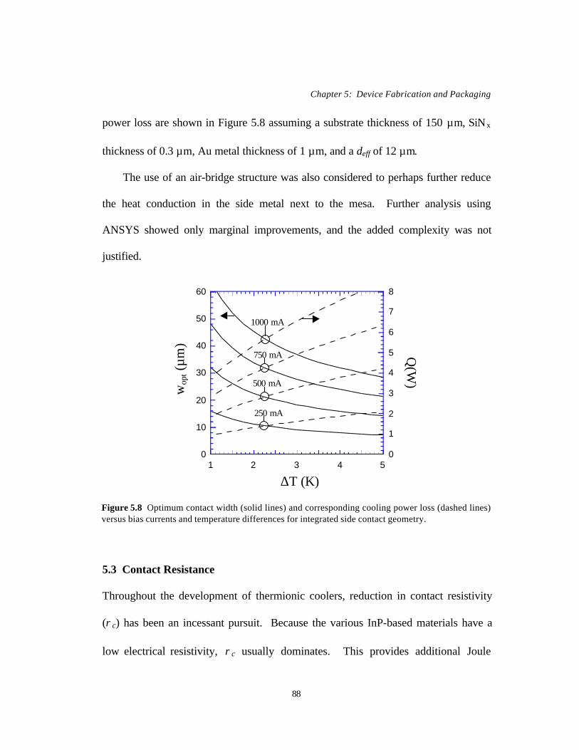
Chapter 5: Device Fabrication and Packaging
88
power loss are shown in Figure 5.8 assuming a substrate thickness of 150 µm, SiNx
thickness of 0.3 µm, Au metal thickness of 1 µm, and a deff of 12 µm.
The use of an air-bridge structure was also considered to perhaps further reduce
the heat conduction in the side metal next to the mesa. Further analysis using
ANSYS showed only marginal improvements, and the added complexity was not
justified.
5.3 Contact Resistance
Throughout the development of thermionic coolers, reduction in contact resistivity
(ρc) has been an incessant pursuit. Because the various InP-based materials have a
low electrical resistivity, ρc usually dominates. This provides additional Joule
Figure 5.8 Optimum contact width (solid lines) and corresponding cooling power loss (dashed lines)versus bias currents and temperature differences for integrated side contact geometry.
0
10
20
30
40
50
60
0
1
2
3
4
5
6
7
8
1 2 3 4 5
∆T (K)
wop
t (µm
)Q
(W)
250 mA
500 mA
750 mA
1000 mA

Chapter 5: Device Fabrication and Packaging
89
heating very close to the cooling region of the device and must be minimized to
attain any appreciable cooling. Since all of the contact regions in the device
structure are InGaAs, only contacts to this material will be considered.
The transmission line model (TLM) method [1] was used to measure contact
resistivity. This analysis included the measurement of “end resistance” (RE), often
overlooked in other reports on ρc. This additional measurement accounts for the
changing sheet resistance underneath the contact area during the alloying process.
The simple TLM analysis assumes that the sheet resistivity is the same everywhere
and does not change during alloying. The changing sheet resistance alters the
transfer length or effective area of the contact over which the majority of current
passes. RE infers the transfer length from a measurement of voltage drop across the
contact pad. Accurate measurements require very narrow pad widths due to the very
low sheet resisitivity of the metal layer. The pad widths used here were 3 to 20 µm.
The first contact scheme investigated was for n-type InGaAs, and used
Ni/AuGe/Ni/Au (50/1000/100/5000Å). The details of the microstructure after the
alloying process have been studied extensively in the literature [2-4]. The basic idea
is that the Ge diffuses into the semiconductor and acts as a dopant element while the
Ni enhances diffusion and is a wetting layer. Figure 5.9 shows the results for contact
resistivity versus alloying temperature for an InGaAs contact layer doped to
3×1018cm-3. The best values are between 5 and 6×10⁻⁷ Ωcm2 for alloying
temperatures near 425 °C. For the values measured in Figure 5.9, the alloying used a
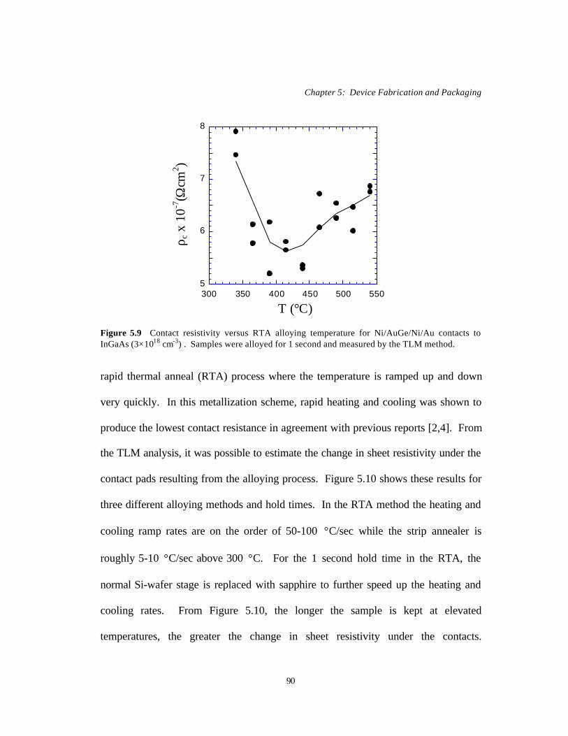
Chapter 5: Device Fabrication and Packaging
90
rapid thermal anneal (RTA) process where the temperature is ramped up and down
very quickly. In this metallization scheme, rapid heating and cooling was shown to
produce the lowest contact resistance in agreement with previous reports [2,4]. From
the TLM analysis, it was possible to estimate the change in sheet resistivity under the
contact pads resulting from the alloying process. Figure 5.10 shows these results for
three different alloying methods and hold times. In the RTA method the heating and
cooling ramp rates are on the order of 50-100 °C/sec while the strip annealer is
roughly 5-10 °C/sec above 300 °C. For the 1 second hold time in the RTA, the
normal Si-wafer stage is replaced with sapphire to further speed up the heating and
cooling rates. From Figure 5.10, the longer the sample is kept at elevated
temperatures, the greater the change in sheet resistivity under the contacts.
T (°C)
ρ c x
10-7
(Ωcm
2 )
Figure 5.9 Contact resistivity versus RTA alloying temperature for Ni/AuGe/Ni/Au contacts toInGaAs (3×1018 cm-3) . Samples were alloyed for 1 second and measured by the TLM method.
5
6
7
8
300 350 400 450 500 550

Chapter 5: Device Fabrication and Packaging
91
Generally, however, this is at the expense of an increased contact resistance and little
advantage is gained from the enhanced sheet resistivity.
If higher doping is used in the InGaAs contact layer, the extra Ge-doping and
alloying process is unnecessary. In this case, unalloyed contacts are attractive since
careful control over the alloying process is no longer needed. Also, there is no
alteration of the semiconductor underneath the contacts which is desirable for
reliability issues. Ti/Pt/Au (150/1000/5000Å) was investigated for contacts to n-type
InGaAs doped around 1.5-2.0×1019 cm-3. In this metallization recipe, the Ti acts as
both an adhesion layer and barrier component. The high dopant concentration allows
SA 30”
ρ sk/ρ
s
Figure 5.10 Ratio of alloyed to unalloyed sheet resistivity versus alloying method and hold time forNi/AuGe/Ni/Au contacts to n-type InGaAs (3×1018 cm-3). RTA stands for a rapid thermal annealprocess while SA represents a slower strip anneal process.
0
0.02
0.04
0.06
0.08
0.1
0.12
0.14
RTA 5”RTA 1”

Chapter 5: Device Fabrication and Packaging
92
for a large field emission providing that the native oxide is not too thick [5]. The Pt
layer prevents Au penetration into the underlying layers. A thickness of at least
1000Å is required for annealing up to 450 °C, and 2000 Å if the device is to undergo
extended high temperature operation [6]. Figure 5.11 shows ρc versus annealing
temperature, which was performed in the strip annealer and held for 20 seconds. The
contact resistance was found to be relatively independent of the heating and cooling
procedure, and a good value is even obtained with no annealing at all.
P-type contacts were also investigated, however only highly doped InGaAs
(2×1019cm-3) was examined. The same Ti/Pt/Au metallization was used as in the n-
type case. The use of a common contact for both p- and n-type coolers is expected to
T (°C)
ρ c (Ω
cm2 )
Figure 5.11 Contact resistivity versus alloying temperature for Ti/Pt/Au contacts to n-type InGaAs(2×1019cm-3) . Samples were alloyed for 20 seconds and measured by the TLM method.
5.0 10-8
1.0 10-7
1.5 10-7
2.0 10-7
2.5 10-7
3.0 10-7
200 250 300 350 400 450noanneal
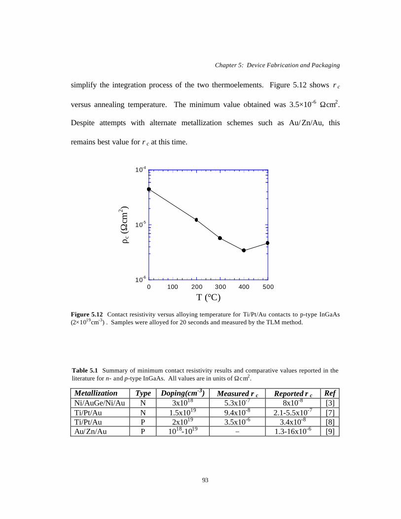
Chapter 5: Device Fabrication and Packaging
93
simplify the integration process of the two thermoelements. Figure 5.12 shows ρc
versus annealing temperature. The minimum value obtained was 3.5×10⁻⁶ Ωcm2.
Despite attempts with alternate metallization schemes such as Au/Zn/Au, this
remains best value for ρc at this time.
Metallization Type Doping(cm-3) Measured ρc Reported ρc RefNi/AuGe/Ni/Au N 3x10¹⁸ 5.3x10⁻⁷ 8x10⁻⁸ [3]Ti/Pt/Au N 1.5x10¹⁹ 9.4x10⁻⁸ 2.1-5.5x10⁻⁷ [7]Ti/Pt/Au P 2x10¹⁹ 3.5x10⁻⁶ 3.4x10⁻⁸ [8]Au/Zn/Au P 1018-1019 − 1.3-16x10-6 [9]
Table 5.1 Summary of minimum contact resistivity results and comparative values reported in theliterature for n- and p-type InGaAs. All values are in units of Ωcm2.
T (°C)
ρ c (Ω
cm2 )
Figure 5.12 Contact resistivity versus alloying temperature for Ti/Pt/Au contacts to p-type InGaAs(2×1019cm-3) . Samples were alloyed for 20 seconds and measured by the TLM method.
10-6
10-5
10-4
0 100 200 300 400 500

Chapter 5: Device Fabrication and Packaging
94
A summary of the presented results and comparative values reported in the
literature are shown in Table 5.1. The measured values for n-type InGaAs compare
fairly well with the best reported numbers. The very best reported value of 4.3×10⁻⁸
Ωcm2 was for higher doped material (5×1019 cm-3) [10]. Generally speaking, if the
doping is greater than 1×1019 cm-3, then the Ti/Pt/Au metallization should be used.
Otherwise for lower dopings, the Ni/AuGe/Ni/Au contacts should be considered for
n-type material, and Au/Zn/Au contacts for p-type material. Further work is needed
to reduce the contact resistance for our p-type InGaAs, as our best value is two
orders of magnitude higher than the best reported value.
5.4 Substrate Transfer
A more in depth and quantitative analysis of substrate thermal resistance will be
presented in Chapter 6, yet the incentive for attempting substrate transfer should be
evident from a simple estimation. While the thermal conductivity of the thermionic
cooler layers is at least an order of magnitude smaller than InP, the thermal
resistance of the substrate can be as large or even larger than the cooler layers due to
the greater thickness. This results in a significant amount of heat flowing back to the
cold side of the cooler, reducing the efficiency. The efforts for replacing the InP
substrate with a higher thermally conducting one such as silicon, copper, or even
diamond, are described in this section.

Chapter 5: Device Fabrication and Packaging
95
The processes for substrate transfer considered here can be categorized as either
bonded or deposited. Bonded refers to the joining of the epitaxial grown layers to a
surrogate substrate where the original substrate is removed before or after the union.
In most cases an intermediate material, such as a metal, solder, or epoxy, is used to
facilitate a complete and uniform junction. A deposited process means that the new
substrate is actually formed directly on the epitaxial layers such as in vacuum
evaporation or electroplating. In any of these above cases, careful attention must be
paid to the material properties and a trade-off between the coefficient of thermal
expansion (CTE) and thermal conductivity (β) is often the issue. Figure 5.13 shows
the CTE and β for the semiconductors, metals, and bonding materials considered
0
50
100
150
200
250
300
350
400
0 5 10 15 20
Cu
Au
BeO
AlN
Si
NiPt
GaAsTi
InP
InGaAs epoxy
Diamond(β=1200)
(CTE=31)
CTE (10-6 K-1)
β (W
/m⋅K
)
Figure 5.13 Thermal conductivity and coefficient of thermal expansion for materials relevant tosubstrate transfer processes.
Sn
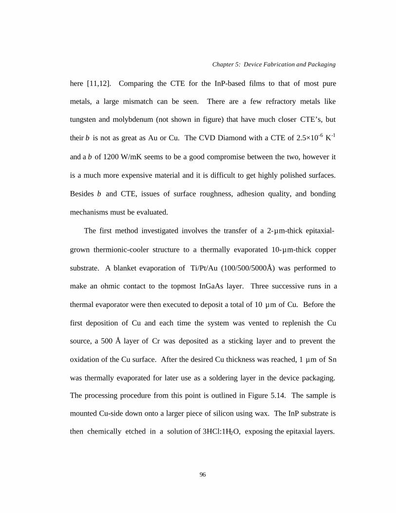
Chapter 5: Device Fabrication and Packaging
96
here [11,12]. Comparing the CTE for the InP-based films to that of most pure
metals, a large mismatch can be seen. There are a few refractory metals like
tungsten and molybdenum (not shown in figure) that have much closer CTE’s, but
their β is not as great as Au or Cu. The CVD Diamond with a CTE of 2.5×10⁻⁶ K-1
and a β of 1200 W/mK seems to be a good compromise between the two, however it
is a much more expensive material and it is difficult to get highly polished surfaces.
Besides β and CTE, issues of surface roughness, adhesion quality, and bonding
mechanisms must be evaluated.
The first method investigated involves the transfer of a 2-µm-thick epitaxial-
grown thermionic-cooler structure to a thermally evaporated 10-µm-thick copper
substrate. A blanket evaporation of Ti/Pt/Au (100/500/5000Å) was performed to
make an ohmic contact to the topmost InGaAs layer. Three successive runs in a
thermal evaporator were then executed to deposit a total of 10 µm of Cu. Before the
first deposition of Cu and each time the system was vented to replenish the Cu
source, a 500 Å layer of Cr was deposited as a sticking layer and to prevent the
oxidation of the Cu surface. After the desired Cu thickness was reached, 1 µm of Sn
was thermally evaporated for later use as a soldering layer in the device packaging.
The processing procedure from this point is outlined in Figure 5.14. The sample is
mounted Cu-side down onto a larger piece of silicon using wax. The InP substrate is
then chemically etched in a solution of 3HCl:1H2O, exposing the epitaxial layers.
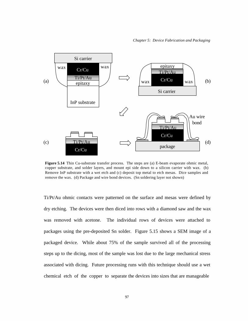
Chapter 5: Device Fabrication and Packaging
97
Ti/Pt/Au ohmic contacts were patterned on the surface and mesas were defined by
dry etching. The devices were then diced into rows with a diamond saw and the wax
was removed with acetone. The individual rows of devices were attached to
packages using the pre-deposited Sn solder. Figure 5.15 shows a SEM image of a
packaged device. While about 75% of the sample survived all of the processing
steps up to the dicing, most of the sample was lost due to the large mechanical stress
associated with dicing. Future processing runs with this technique should use a wet
chemical etch of the copper to separate the devices into sizes that are manageable
Au wirebond
(a) (b)
(c) (d)
InP substrate
epitaxyTi/Pt/Au
Cr/Cu
Si carrier
wax wax epitaxyTi/Pt/Au
Cr/Cu
Si carrier
wax wax
Ti/Pt/Au
Cr/Cu
Ti/Pt/Au
Cr/Cu
package
Figure 5.14 Thin Cu-substrate transfer process. The steps are (a) E-beam evaporate ohmic metal,copper substrate, and solder layers, and mount epi side down to a silicon carrier with wax. (b)Remove InP substrate with a wet etch and (c) deposit top metal to etch mesas. Dice samples andremove the wax. (d) Package and wire bond devices. (Sn soldering layer not shown)

Chapter 5: Device Fabrication and Packaging
98
with vacuum tweezers. The maximum cooling achieved with this device was only
0.1 °C, which compares poorly to the same structure processed on the growth
substrate that cooled by 0.7 °C. This is likely due to the large thermal resistance at
the interface between the copper and the package. Specifically, the solder layer was
not performing as desired and large voids were present. The SEM photo in Figure
5.15 indicates that there is indeed an air gap in this region. While the packaging
continues to be a challenge for the Cu-substrate samples, the process itself appears to
work adequately. No cracking or bowing of the epitaxial layer was observed, even
though film stress values have been reported in the range of 50 MPa for sputtered Au
[13]. Electroplating is known to result in thin metal films with much less stress on
Cu Substrate
Cooler
Gap
Figure 5.15 SEM of a packaged thin-film thermionic cooler on a 10-µm-thick copper substrate. Itis clear from the photo that there are large gaps that the solder did not spread to during packaging.
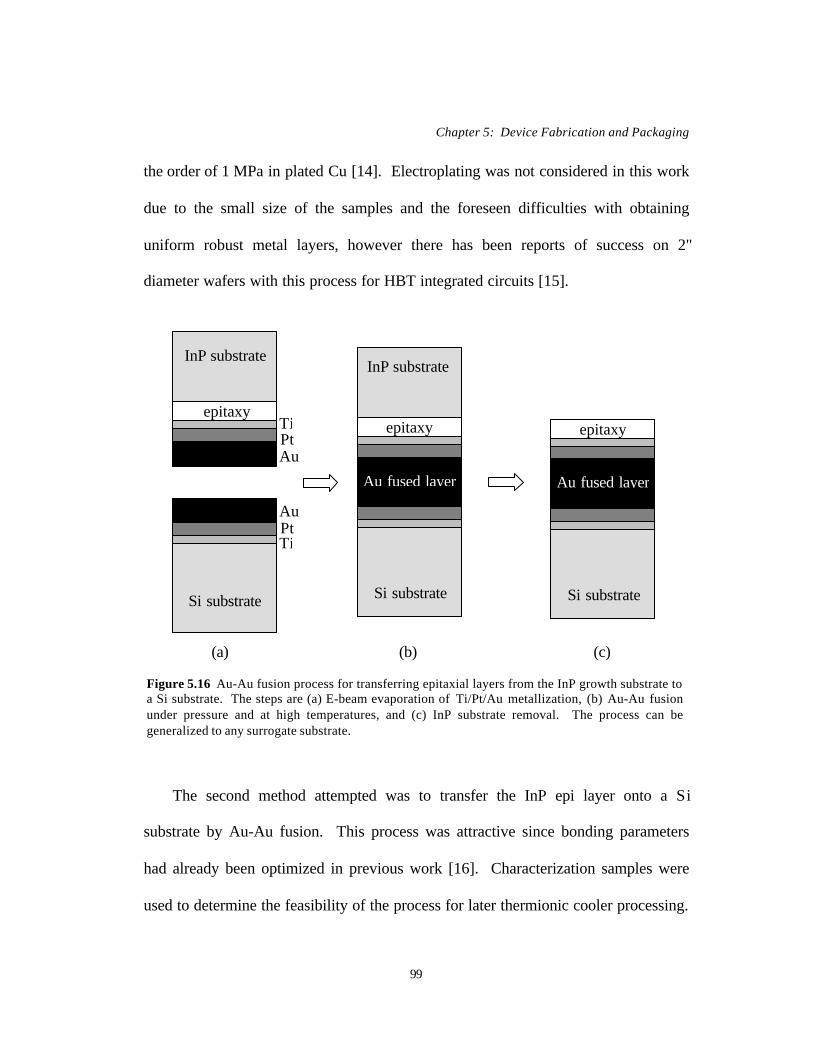
Chapter 5: Device Fabrication and Packaging
99
the order of 1 MPa in plated Cu [14]. Electroplating was not considered in this work
due to the small size of the samples and the foreseen difficulties with obtaining
uniform robust metal layers, however there has been reports of success on 2"
diameter wafers with this process for HBT integrated circuits [15].
The second method attempted was to transfer the InP epi layer onto a Si
substrate by Au-Au fusion. This process was attractive since bonding parameters
had already been optimized in previous work [16]. Characterization samples were
used to determine the feasibility of the process for later thermionic cooler processing.
TiPtAu
AuPtTi
(a) (b) (c)
InP substrate
epitaxy
Si substrate
Au fused layer
InP substrate
epitaxy
Si substrate
Au fused layer
epitaxy
Si substrate
Figure 5.16 Au-Au fusion process for transferring epitaxial layers from the InP growth substrate toa Si substrate. The steps are (a) E-beam evaporation of Ti/Pt/Au metallization, (b) Au-Au fusionunder pressure and at high temperatures, and (c) InP substrate removal. The process can begeneralized to any surrogate substrate.

Chapter 5: Device Fabrication and Packaging
100
Figure 5.16 shows the steps used in the Au-Au bonding. After sample cleaning,
metal layers of Ti/Pt/Au 500/1000/15000Å were deposited by e-beam evaporation.
The samples were then brought into contact and held under pressure (~ 70 kPa) using
a rubber-boot vacuum fixture on a hot plate. The temperature was ramped up at
1°C/min to a temperature of 350 °C, held for five minutes, and then ramped down at
the same rate. The slow ramping was to reduce stress caused by the CTE mismatch
between the wafer and metal. After the fusion, the InP substrate was etched off, and
the remaining epi layers were examined under an optical microscope. Of the two
samples bonded, only one appeared to have most of its surface fused and void
bubbles were present in several places on the sample. Evaporating a thin layer of Sn
after the Au evaporation is expected to help with the reliability of this process since
the solder can actually reach its melting temperature and reflow to fill in any voids.
Any addition of Sn would increase the thermal resistance, and must be considered
when deciding how thick a layer to use.
In a variation of the previous procedure, Au-Au fusion using a diamond
substrate (1 cm2 area, 300 µm thick) was briefly attempted. It became evident early
on that the CVD-grown substrates used were not planar enough and showed a
bowing across the surface of 3 µm and a maximum surface roughness of 1.2 µm.
Highly planar samples and crystallographic surfaces are necessary for high quality
Au-Au fusion. The use of Sn was employed in order to planarize the surface, but
even with 5 µm of evaporated Sn, difficulties achieving a good bond were

Chapter 5: Device Fabrication and Packaging
101
encountered. Smoother and more planar diamond samples are needed to improve the
bonding without sacrificing the benefits of thermal conductivity by using thick solder
layers.
5.5 Summary
In this chapter we discussed the basic processing procedures used for heterostructure
integrated thermionic coolers. The steps are kept as simple as possible to facilitate
their integration with optoelectronic devices. To characterize the single-stage
coolers, packaging is required. The goal of packaging is to allow for the
measurement of the intrinsic device without effecting the measurement itself. Three
generations of packaging were presented, and the improvements in each discussed.
It is believed that we are nearly at the limit of optimizing the packaging, and further
improvements in single-stage performance must come from the device design.
The minimum contact resistivity values for n-type InGaAs are also close to
being fully optimized and compare well with the best values reported in literature.
P-type contact resistance still needs further reduction which should be possible.
Ti/Pt/Au contacts are generally preferred for both n- and p-type contacts as long as
the InGaAs material is doped to at least 1019 cm-3.
Several prospects exist for transferring the InP-based epitaxial layers from the
InP growth substrate to a surrogate substrate with a higher thermal conductivity.
Moderate success was obtained with the thin Cu-film process, but handling and
Chapter 5: Device Fabrication and Packaging
102
packaging problems were encountered. Au-Au bonding to Si or Cu substrates seems
feasible. Diamond substrates are preferred, however highly polished surfaces are
needed.
REFERENCES
1. G.K. Reeves, H.B. Harrison, “Obtaining the Specific Contact Resistance from Transmission LineModel Measurements,” Elec. Dev. Lett., Vol. EDL-3, No.5, 1982, p. 111-3.
2. M. Ogawa, “Alloying behavior of Ni/Au-Ge films on GaAs,” J. Appl. Phys. Vol.51, No.1, 1980,p. 406-12.
3. H. Kraulte, E. Woelk, J. Selders, H. Beneking, “Contacts on GaInAs,” IEEE Trans. Elec. Dev.,Vol. ED-32, No.6, 1985, p.1119-23.
4. G.Y. Robinson, “Metallurgical and electrical properties of alloyed Ni/Au-Ge films on n-typeGaAs,” Solid-State Electronics, Vol.18, No.4, 1995, p. 331-42.
5. S.M. Sze, Physics of Semiconductor Devices. New York: Wiley, 1981.
6. G. Robinson (personal communication , May 8, 1999).
7. L.G. Shantharama, H. Schumacher, H.P. Leblanc, R. Esagui, R. Bhat, M. Koza, “Evaluation ofsingle ohmic metallizations for contacting both p- and n-type GaInAs,” Elec. Lett., Vol.26,No.15, 1990, p.1127-9.
8. A. Katz et al, “Pt/Ti/p-InGaAs low-resistance nonalloyed ohmic contact formed by rapid thermalprocessing,” Applied Physics Letters, Vol.54, No.23, 1989, p.2306-8.
9. A.D. Huelsman, C.G. Fonstad, “Fabrication and Characterization of nonalloyed Cr/Au ohmiccontacts to n- and p-type InGaAs,” IEEE Trans. Elec. Dev., Vol. ED-33, No.2, 1986, p.294-7.
10. G. Stareev, H. Kunzel, G. Dortmann, “A controllable mechanism of forming extremely low-resistance nonalloyed ohmic contacts to group III-V compound semiconductors,” J. Appl. Phys.,Vol.74, No.12, 1993, p.7344-55.
11. D.R. Lide, CRC Handbook of Chemistry and Physics. New York: CRC Press, 1991.
12. P. Bhattacharya, Properties of Lattice-Matched and Strained InGaAs, London, UK: INSPEC,1993.
13. T.C. Hodge, S.A. Bidstrup-Allen, P.A. Kohl, “Stresses in thin film metallization,” IEEETransactions on Components, Packaging, and Manufacturing Technology, Part A, 20, 1997,p.241-50.
Chapter 5: Device Fabrication and Packaging
103
14. F.A. Lowenhiem, Modern Electroplating. New York: Wiley, 1974.
15. M. Rodwell, Q. Lee, D. Mensa, J. Guthrie, S.C. Martin, R.P. Smith, R. Pullela, B. Agarwal, S.Jaganathan, T. Mathew, S. Long, “Transferred-substrate HBT integrated circuits ,” Solid-StateElectronics, Vol. 43, 1999, p. 1489-95.
16. D. Tauber, M. Horita, J. Piprek, P. Abraham, A.L. Holmes, J.E. Bowers, “The microstrip laser,”Photonics Technology Letters, Vol. 10, 1998, p. 478-80.

Chapter 5: Device Fabrication and Packaging
104

Chapter 6: Cooling Results and Analysis
105
Chapter 6
Cooling Results and Analysis
Before moving forward with the integration of thermionic coolers with
optoelectronic devices, it is first necessary to fully characterize and optimize the
individual cooler. In the last chapter, the evolution of packaging for effective heat
sinking and electrical connections for testing was described. Our first challenge here
is with the measurement of temperature itself. The device areas considered range
from 200×200 µm2 to as small as 10×10 µm2. In many cases, not only the average
temperature over such areas is desired, but the actual temperature distribution.
Several commercial vendors claim to have characterization equipment that can
measure temperature with sub-degree or sub-micron precision, but none are capable
of high spatial and temperature resolution simultaneously. Consequently, novel
small-scale temperature characterization systems needed to be developed. The first
section of this chapter is devoted to these characterization solutions and techniques.
The section following presents the experimental results and analysis for various
device sizes, ambient temperatures, superlattice designs, and material types. A new
type of cooler structure is also presented that integrates together a thermionic and
thermoelectric (TITE) cooler structure into a two-stage three-terminal device. The
non-ideal effects that impede our arrival to the intrinsic device limitations are then
discussed in detail. Finally, simulations to model and explain the device operation,

Chapter 6: Cooling Results and Analysis
106
including the non-ideal effects, are given. These simulations are then used to predict
improvements in performance as the non-ideal effects are reduced.
6.1 Measurement Techniques
The measurement methods described below can be categorized into either contact or
non-contact implementations. The contact techniques involve either the manual
placement or the integration of a temperature sensor with the cooler, while the non-
contact techniques measure the temperature indirectly by monitoring such things as
reflectivity or emissivity. The advantages and disadvantages are described in each
specific case.
6.1.1 Micro-Thermocouples
The micro-thermocouple measurement has been used for the majority of temperature
characterization due to its robustness and ease of testing many devices quickly. The
set-up is shown in Figure 6.1. As in many of the temperature measurement systems,
the sample is placed on a temperature-controlled copper stage using thermal
compound to ensure good contact with the heat sink. Two thermocouple wires (1-2
mil diameter, type E) are mounted on micro-positioners where a positive and
negative lead are attached and the remaining two leads connect to a voltmeter. The
reference thermocouple is kept on the stage while the measurement thermocouple is
placed on the cooler. Normally, for atmospheric conditions, a thin layer of moisture

Chapter 6: Cooling Results and Analysis
107
is present on all surfaces that allows for an adequate thermal connection between the
thermocouple and cooler. However, it was determined that the temperature results
were more reproducible when a small amount of thermal compound was used as a
thermal interface. With the stage kept at constant temperature, the two micro-
thermocouples are used in a differential measurement of temperature as the current
bias is varied. A computer along with LabVIEW [1] software was used to control all
instrumentation and automate the measurement process with the only exception
being the thermocouple placement.
MeasurementThermocouple
ReferenceThermocouple
BottomContact
TopContact
InGaAsEmitter
SuperlatticeBarrier
InGaAsCollector
Figure 6.1 Micro-thermocouple characterization set-up. The stage is kept at constant temperaturewhile two micro-thermocouples are used in a differential measurement of temperature for variouscurrent biases. The external or integrated wire bond is not shown.
Temperature Controlled Stage
InP Substrate

Chapter 6: Cooling Results and Analysis
108
Using this system, point measurements anywhere on the surface were possible
within the limits of the thermocouple size. While thermocouple wire diameters as
small as 1 mil were used, the actual junction was typically twice that size. Only
devices down to around 40×40 µm2 could reliably be tested, and even then the
thermocouple would present a significant thermal conduction path and affect the
measurement. Nonetheless, superb temperature resolutions of below 0.01 °C were
possible, with response times less than 100 µs. Many of the results shown in Section
6.2 used this system.
6.1.2 Integrated Platinum Heaters
Platinum material is used extensively in resistive temperature devices (RTD’s). As
their name implies, these types of devices use the fact that the electrical resistance of
metals change with temperature. For Pt, in the range of 0 to 100 °C, the resistance
changes nearly linearly with a temperature coefficient of 3.929×10⁻³ K-1. In our case,
Pt metal lines were lithographically defined on top of the cooler as in Figure 6.2.
These lines not only worked as temperature sensors, but also as variable heaters to
measure the cooling versus heat load. While valuable heat load characterization
could be made on the larger devices, the Pt resistors did not scale well for small
devices since metal lines could not be made long enough. Even the longer wires on
the larger devices did not match the resolution of the micro-thermocouple system,
and little advantage in temperature measurement was seen. Furthermore, the

Chapter 6: Cooling Results and Analysis
109
additional thermal conduction paths of the connections for the resistors and SiN x
isolation layer resulted in reduced cooling by as much as 50% when compared with
normal devices. In spite of this, specific applications such as transient testing or
measurement in vacuum still exist for the Pt resistors.
6.1.3 Integrated Optoelectronic Devices
The operational characteristics of most optoelectronic devices are by nature
temperature dependant. These characteristics can therefore be correlated to
temperature as a measurement method. For instance, in the case of p-i-n detectors
the temperature-dependent current-voltage relationship can be used to measure
temperature [2]. A more familiar example is the use of wavelength shift or output
power in lasers. Figure 6.3 illustrates some of these characteristics versus
Figure 6.2 SEM image of a cooler with a patterned Pt-heater on top. The Pt metal was electricallyisolated from the top of the cooler with a thin layer of SiNx.

Chapter 6: Cooling Results and Analysis
110
temperature. Further discussion of integrated structures will be postponed until
Chapter 7.
Figure 6.3 Temperature dependent properties of some optoelectronic devices (a) A p-i-n InP diodeunder constant current has a temperature dependent voltage. (b) The wavelength and optical powerof a DFB laser diode are also temperature dependent.
0.92
0.93
0.94
0.95
0.96
15 20 25 30T (°C)
Vol
tage
(V)
CmV
TV
o2−=∆∆
1542.70
1542.75
1542.80
1542.85
1542.90
-23
-22
-21
-20
-19
-18
-17
-16
-15
18 18.5 19 19.5 20 20.5
T (°C)
λ (n
m)
Cnm
T o1.0=∆∆λ
Power (dB
m)
CdBm
TP
o4−=∆∆
(a)
(b)

Chapter 6: Cooling Results and Analysis
111
6.1.4 IR Camera
Infrared cameras have found numerous uses in macroscopic temperature
measurement, especially when the temperatures are extremely high and exceed the
range of contact-type sensors. Recently they have also found applications in
microscopic thermal imaging [3,4] as new advances in the technology have emerged.
In conjunction with precision optics, the IR camera systems can produce thermal
images of surfaces with temperature resolutions of a few degrees and spatial
resolutions of 10’s of microns.
The basic experimental set-up was controlled by a PC which coordinated the
timing of the camera snapshots and the pulse generator that applied the signal to the
device [3,5]. The camera captured 3-5 µm IR radiation on a 256 × 256 InSb focal
plane array detector. Each of the 65,536 detectors formed a single pixel in the final
image.
While qualitative data of heating and cooling could be collected using this
technique, the temperature resolution was not adequate and reproducibility was
difficult. This is most likely attributed to the poor emissivity of smooth metals
(<20%) which cover the top of the cooler surface allowing for a large portion of the
signal to come from reflected radiation off other sources. The emissivity of an
opaque material is in general inversely proportional to its reflectivity. When
measuring the surface of a low emissivity material, much of the energy reaching the
sensor can be reflection from other nearby emitters. This effectively increases the

Chapter 6: Cooling Results and Analysis
112
noise in the signal. In the next section, an alternative method for temperature
imaging is described which solves many of the problems encountered with the
infrared system.
6.1.5 Thermoreflectance
The thermoreflectance technique is based on the temperature-induced reflectivity
change in materials. All materials exhibit this change, albeit small in most cases. By
monitoring the change in intensity of reflected light, the surface temperature can be
determined [6-8]. Due to the small change in reflectivity (∆R/∆T~2×10-5 /°C), a
lock-in technique is needed to detect the signal.
The measurement system is shown in Figure 6.4 (developed by James
Christofferson). The device is illuminated with a white light source and biased with
current pulses at 200 Hz to allow for heterodyne filtering. A magnifying objective
and beamsplitter are used to image the reflected signal on to the detector. The
detector used was a Hammamatsu 16×16 photodiode array. Calibration is
accomplished by normalizing to previously measured temperature measurements
using the micro-thermocouple system. Only the large devices are used for
calibration so that the thermocouple size does not affect the cooling.
This method has proved to be indispensable in the mapping of temperature
profiles across the surface of coolers. High quality images of the coolers have been
successfully measured with 100 mK temperature and sub-micron spatial resolution.

Chapter 6: Cooling Results and Analysis
113
6.2 Experimental Results
The first experimental demonstrations of cooling were modest to say the least. An
example of an early cooling result is shown in Figure 6.5. A humble 0.05 K of
cooling was measured around 60mA of current for a 3200 µm2 device size. Still, the
successful measurement of such a small temperature change was encouraging as it
allowed for analysis as to the limitations on performance. By fitting the data points
with a second order polynomial, the linear and quadratic components could be
quantified. As in conventional TE coolers, the linear coefficient represents the
Peltier cooling or heating effects in the device (∝ I ) and the quadratic coefficient
describes the Joule heating contributions (∝ I2 ). By observing how these
coefficients change versus device size, geometry, ambient temperature, superlattice
Illuminator
Beamsplitter
80× Objective
TE controlled X-Ytranslation stage
Device signal
Enlarged imageincident on
detector array
Figure 6.4 Experimental setup for thermoreflectance measurement system. The diffraction limit ofvisible white light from the illuminator bounds the spatial resolution to a sub-micron scale.

Chapter 6: Cooling Results and Analysis
114
design, and other conditions, conclusions can be made about optimum design
parameters or limitations from non-ideal effects. The results discussed in this section
are for single-stage coolers. More complex, integrated structures are analyzed in
Chapter 7.
Before discussing the results, a more in-depth look at the qualitative device
operation would be useful. The device can be broken into three regions as shown in
Figure 6.6, where the electrical conductivity (σn), thermal conductivity (βn), and area
(An) are defined for the nth region. The equivalent circuit model is shown on the
right with the arrows indicating sources or sinks of heat flux. QTI refers to
-0.1
-0.05
0
0.05
0.1
0 50 100 150 200
I (mA)
Coo
ling
(K)
Figure 6.5 One of the first experimental results demonstrating cooling. The thermionic coolerstructure consisted of a simple 1 µm thick n-type InGaAsP-barrier (1×1017cm-3) between InGaAsemitter and collector regions (2.8×1018cm-3). The device area was 3200µm2. Small cooling in thisearly device was limited by the packaging and contact resistance.

Chapter 6: Cooling Results and Analysis
115
thermionic heating/cooling, QTE to thermoelectric cooling (metal-semiconductor
interface), and QC to heat generation by contact resistance. From circuit analysis, an
expression can be found for the temperature at the cold side of the device (between
regions 1 & 2). If the thermal resistance of the wire (Rwth) is much less than the sum
of the cooler and substrate thermal resistance, it can be neglected to simplify the
analysis. Likewise, the electrical resistance of the substrate can be ignored compared
to the other regions. The resulting expression is:
where Rdth and Rsub
th are the cooler and substrate thermal resistances, and RAu and RC
are the gold wire and contact electrical resistances respectively. QTE and QTI
2))(21
())(( IRRRRRQRRQQT thsub
thdCAu
thsubTI
thsub
thdTETI ++−−++=∆ (6.1)
QTI + QTE – QC
Region 1: Au wireσw, κw, Aw
Region 2: cooler σc, κc, Ac
Region 3: substrateσs, κs, As
Heat Sink: T = 300K
Heat Sink: T = 300K
Lw
Lc
Ls
Rw
Rc
Rs
- QTI
Figure 6.6 One-dimensional model and boundary conditions. Electrical conductivity (σ), thermalconductivity (β), and area (A), are defined in each region. The equivalent circuit model is shown onthe right with the arrows indicating sources or sinks of heat flux. QTI refers to thermionicheating/cooling, QTE to thermoelectric cooling, and QC to heat generation by contact resistance.

Chapter 6: Cooling Results and Analysis
116
comprise the linear term (I is located inside the expressions) as mentioned above.
Likewise, the second term containing the electrical resistances is proportional to the
square of current. Each term is also scaled by a factor that describes the thermal
resistances between the heat sources and sinks. This equation is similar in form to
the expression for conventional thermoelectrics (Equation A.1, Appendix A), but
includes all of the important non-ideal parameters for thin film coolers such as
contact resistance, wire bond heat load, and substrate thermal resistance.
6.2.1 Cooling Vs. Size
Most of the terms in Equation 6.1 are area dependent, and so studying the cooling
dependence on device size provides much information about the behavior of the
device. The measured cooling versus current density for several device areas is
shown in Figure 6.7a for the low-barrier InGaAs/InGaAsP structure described in
Chapter 3 (Section 3.2). At low current densities, all the devices operate nearly
identically as expected. As the current is increased, the area dependent non-ideal
heating contributions become apparent. The smallest size device (5000µm2) cools
best because it requires less current to reach a given current density, and the rollover
occurs later. Referencing Equation 6.1, the curves in Figure 6.7a can be fitted with a
second order polynomial and the corresponding linear and quadratic coefficients
extracted. Figure 6.7b plots these coefficients versus area. Using Equation 6.1 and
the known material properties, the area dependence can be modeled and the device

Chapter 6: Cooling Results and Analysis
117
0
0.2
0.4
0.6
0.8
1
1.2
1.4
0 4000 8000 12000
(a)
J (A/cm2)
Coo
ling
(K)
5000µm2
7200µm2
16200µm2
20000µm2
1
2
3
4
5
6
-8
-7
-6
-5
-4
-3
-2
-1
0 5000 10000 15000 20000 25000
(b)
Area (µm2)
Line
ar C
oeff
icie
nt (K
/A)
Quadratic C
oefficient (K/A
2)
Figure 6.7 (a) Cooling versus current density for several device sizes and (b) the correspondinglinear (cooling) and quadratic (heating) coefficients from a second order polynomial fit as in Equation6.1. The points are the experimental values, and the curves are simulated from Equation 6.1.Measurements were performed with a heat sink temperature of 300K.
Chapter 6: Cooling Results and Analysis
118
operation understood. The term RAu is area independent, the terms Rdth and RC are
proportional to 1/area, and the term Rsubth is proportional to 1/√area. Thus the
following proportionalities result:
The values assumed in the curve fits of Figure 6.7b are listed below in Table 6.1.
Fitting the linear coefficient is fairly straightforward if accurate values of QTI and
QTE can be determined. In this analysis, QTE was first estimated from theoretical
values as well as Seebeck measurements on InGaAs test structures. QTI was then
adjusted to account for the additional cooling necessary to fit the experimental
results. The need for an additional cooling term is evidence that thermionic cooling
is indeed taking place, and in this case it accounts for 78% of the total cooling. The
thermal and electrical resistance values used considered full 3D self-consistent
electrical and thermal simulations where appropriate (the 3D simulations will be
discussed in Section 6.4). Using a power fit, the area dependence was 1/A0.75,
indicating that both terms of Equation 6.2 are important. The more challenging task
is the curve fit for the many terms of the quadratic coefficient. For this, estimated
values of resistance were used for all terms except Rsubth, which was used as a fitting
coefficient. The value chosen must be carefully considered to satisfy both the linear
and quadratic expressions. An adequate curve fit for the quadratic term necessitated
AAlinear 11
2/1+∝
22/32/1
1111AAAA
quadratic +++∝
(6.2)
(6.3)

Chapter 6: Cooling Results and Analysis
119
all of the terms of Equation 6.3, and neglecting any one term would compromise a
good fit. Area dependence with a power fit was 1/A0.9. The encouraging conclusion
from this, is that an improvement in any one of the non-ideal effects should improve
the cooling result. While the approximations made here helped to gain an intuitive
feeling for the device operation, a complete analysis should include all relevant
parameters. A more exhaustive model and device simulation are presented later.
Parameter Description Value [units]Lw Au wire length 600 [µm]Aw Au wire cross-sectional area 507 [µm2]ρw Au wire resistivity 0.0227 [Ω µm]ρc Contact resistivity 50 [Ω µm2]Lc Cooler thickness 1 [µm]βc Cooler thermal conductivity 4×10⁻⁶ [W/µm⋅K]βs Substrate thermal conductivity 68×10-6 [W/µm⋅K]
QTI / I Thermionic voltage 0.053 [V]QTE / I Thermoelectric voltage 0.015 [V]
RAu Au wire electrical resistance 0.027 [Ω]Rc Contact resistance 50/A [Ω µm2]Rd
th Cooler thermal resistance 2×10⁵/A [Kµm2/W]Rsub
th Substrate thermal resistance 9632/√A [Kµm/W]
For some devices, an optimum device size is observed as in Figure 6.8a. Since
Equation 6.1 only predicts improved cooling for smaller devices (at least over the
range of device sizes considered here), some other explanation must be found. The
Table 6.1 Important material parameters and calculated resistance values for the curve fits in Figure6.7b. The resistances are calculated from equations of the form L / β⋅A, except for the substratethermal resistance which was used as a fitting parameter.

Chapter 6: Cooling Results and Analysis
120
Figure 6.8 (a) Maximum cooling and corresponding current versus device area showing an optimumdevice size in ∆T due to the heat load from the thermocouple. (b) Increased cooling with thethermocouple heat load removed and the thermoreflectance measurement used (1600 µm2 size).
0.6
0.7
0.8
0.9
1
1.1
1.2
4 10-5
6 10-5
8 10-5
1 10-4
1.2 10-4
0 2000 4000 6000 8000 1 104 1.2 104
Area (µm2)
∆T
max
(K) Jopt (A
/cm2)
(a)
0
0.5
1
1.5
2
2.5
0 100 200 300 400 500
(b)I (mA)
∆T
max
(K)
Thermoreflectance
µ -Thermocouple

Chapter 6: Cooling Results and Analysis
121
first possibility is that for the smallest devices, the wire bond is no longer optimized
and heat conduction through the electrical connection becomes important. This can
be corrected however by optimizing the wire bond for each size device. The other
likely influence is in the measurement itself. For small devices, the thermocouple
becomes much larger than the cooler and presents a considerable heat load. The
effect of the thermocouple for small devices has been verified with the
thermoreflectance measurement, which shows that the smaller devices do still
produce larger cooling as shown in Figure 6.8b.
6.2.2 Cooling Vs. Ambient Temperature
Ideally the height of the heterobarrier and the Fermi level are engineered to be
optimum for a given operating temperature. All of the structures examined were
designed for room temperature operation. The cooling behavior was examined for
various heat sink temperatures to determine the effects. Figure 6.9 shows the cooling
versus current bias at different temperatures for a size 5000 µm2 cooler. The
observed trend is increased cooling at elevated operating temperatures. The origin of
the temperature dependence stems from the change in material properties (thermal
and electrical conductivity) and in the thermionic and thermoelectric cooling
mechanisms. Borrowing from the analogous case of conventional thermoelectrics,
the maximum cooling and optimum current can be expressed as [9],

Chapter 6: Cooling Results and Analysis
122
where (ΦB + 2kBT/e) was used in Chapter 2 as an approximation for the thermionic
effect in the limit of Boltzmann statistics, σ and β are the electrical and thermal
conductivity respectively, and R is the electrical resistance. Over the temperature
range of interest, the effective cooling is approximately ∝ T and thermal conductivity
∝ T -1.4 [10]. The temperature dependence of electrical conductivity is determined by
the mobility which is approximately constant over these temperature values since it
is mostly dominated by impurity scattering. From Equations 6.4 & 6.5, the maximum
cooling and optimum current are roughly proportional to (T 1.4 + T 2.4+ T 3.4) and T
respectively. The data points in Figure 6.9b fit very well to these corresponding
powers. Numerically, the temperature dependence of Iopt is easier to analyze since it
is a simple linear equation. Comparing the fit, Iopt = 380 + 1.51T, with Equation 6.5,
a resistance of 0.114 Ω and a barrier height of 43 meV result. Both values are with
in a factor of two of the expected values. For an analysis over a wider temperature
range, the dependence of the electrical conductivity may have to be estimated, as
well as a more accurate model of the effective cooling using Fermi- Dirac statistics.
ReTk
I BBopt
/2+Φ= (6.5)
βσ2
max)/2(
21 eTk
T BB +Φ=∆ (6.4)

Chapter 6: Cooling Results and Analysis
123
0
0.5
1
1.5
2
2.5
0 100 200 300 400 500 600 700
(a)I (mA)
∆T
(K)
293K
363K
(b)Temperature (K)
∆T
max
(K) Iopt (m
A)
1
1.2
1.4
1.6
1.8
2
2.2
2.4
300
350
400
450
500
550
600
280 300 320 340 360 380
Figure 6.9 (a) Cooling versus current bias for heat sink temperatures of 293-363K in 10Kincrements. (b) Corresponding maximum cooling (solid) and optimum current (dashed) versus heatsink temperature. The points are the experimental values and the curves are the theoretical curve fits,∆Tmax∝ T 1.4 + T 2.4+ T 3.4, Iopt∝ T. ∆T is measured with respect to the heat sink temperature.

Chapter 6: Cooling Results and Analysis
124
In some cases, such as certain IR lasers or photodetectors, cooling at very low
temperatures with solid-state refrigeration is desired. Conventional thermoelectrics
are forced to work with the temperature-dependent bulk cooling-properties of
separate materials, but thermionic cooling in heterostructures can be designed for a
broader range of temperatures by tailoring the barrier height and superlattice to
account for the change in the carrier distribution over temperature. While none of
the structures investigated in this work were designed for low temperature operation,
it is still interesting to observe the behavior for these conditions. Figure 6.10 shows
∆Tmax and Iopt versus heat sink temperature for an 18/7nm InGaAs/InP superlattice.
The measurements were performed in a liquid-N2 cooled low temperature micro-
0.0
0.5
1.0
1.5
2.0
0
100
200
300
400
500
600
50 100 150 200 250 300 350
T (K)
∆T
max
(K)
Figure 6.10 Maximum cooling and optimum current versus heat sink temperature for a 18/7nmInGaAs/InP superlattice design. The measurements were performed in a liquid-N2 cooled lowtemperature micro probe system. The chamber pressure was approximately 10-4 to 10-5 torr. Twomeasurements of ∆Tmax at room temperature and pressure are shown for reference.
Iopt (mA
)
300Katm
Chapter 6: Cooling Results and Analysis
125
probe system with a chamber pressure of approximately 10-4 to 10-5 torr. Even over
this extended temperature range, the data still fits very well to the expressions
derived above. Two measurements of ∆Tmax at room temperature and pressure are
also shown for reference. There was an average increase of 15-20% in ∆Tmax when
testing under vacuum, that is attributed to heat convection through the air.
6.2.3 Cooling Vs. Packaging
The packaging has proven to be an important factor to optimize as mentioned in
Chapter 5. The addition of a package between the substrate and heat sink adds
another thermal barrier for heat to pass through. Improvements in reducing this
added thermal resistance by using silicon or copper packages and by optimizing the
length of the wire bond have resulted in a maximum cooling increase of around
300% in some devices. Ultimately, when the thin film coolers are integrated with
real devices or are packaged in a conventional TE configuration (n- and p-type legs
electrically in series, thermally in parallel for example, see Ref. 9), the issue of
wire bonding will be less of a concern.
Figure 6.11 shows the increase in InGaAs/InGaAsP thermionic cooler
performance for four variations in packages. In each successive package, the cooling
(linear) coefficient remains nearly constant while the heating (quadratic) coefficient
is reduced. The reduction in the heating coefficient can be explained from a
combination of lower contact resistance, wire bond length, and package thermal
Chapter 6: Cooling Results and Analysis
126
resistance. According to Equation 6.1, the former two only effect the heating
coefficient, but the latter quantity should also reduce the linear coefficient. Since
this remains relatively constant, it suggests that either Rdth>>Rsub
th which is not the
case, or that QTI > QTE. The best cooling shown in Figure 6.11 is for a package made
from a 350-µm-thick Si-wafer and using a wire bond length of 250 µm,
corresponding to the second package generation described in Chapter 5. While the
package is near to being fully-optimized for single-stage coolers, estimated reduction
in cooling due to the wire bond is estimated to be as high as 50%. Combined p- and
n-type structures should be used to eliminate this loss.
Figure 6.11 Measured cooling for a 1µm InGaAs/InGaAsP thermionic cooler with various packages.The cooling (linear) and heating (quadratic) coefficients correspond to a second order polynomial fit.The cooling coefficients remain nearly constant while the heating coefficients are reduced. Alltemperatures are relative to the value at zero current with a heat sink temperature of 20 ºC.
0
0.5
1
1.5
0 100 200 300 400 500
I (mA)
∆T
(K)
Cooling coefficient0.00550.00460.00540.0058
Heating coefficient0.6e-50.8e-51.6e-52.8e-5

Chapter 6: Cooling Results and Analysis
127
6.2.4 Cooling Vs. Superlattice Design
With the extrinsic parameters of geometry, temperature, and packaging having been
discussed, the intrinsic parameters of heterostructure design are now examined. The
ultimate goal is of course to maximize the ZT of the effective material.
Unfortunately, the inherent cooling properties of the thin film structure are masked
by the external effects of the substrate and contacts.
One fundamental effect that is difficult to distinguish is the bulk thermoelectric
effect between dissimilar materials, especially at the metal-InGaAs interface. This is
because the thermoelectric effects have the same linear dependence on current as
thermionic emission cooling, and occur very near each other in the device. When
reviewing measurements, the question is raised of how much cooling is due to each
effect? One straightforward approach that attempts to answer this question is a
simple A-B comparison. Structures with and without barriers for thermionic
emission are tested, and the results compared. For example, in the analysis that
included Table 6.1 and Figure 6.7, the thermoelectric Seebeck voltage was estimated
to contribute roughly 30% to the overall cooling term. The ratio of thermionic to
thermoelectric cooling can vary dramatically from structure to structure, and in some
cases the latter is believed to be the dominant effect. The A-B comparison is not an
accurate method for quantifying the cooling effects since the very act of removing
the heterobarriers will also alter the transport properties that define the electrical and

Chapter 6: Cooling Results and Analysis
128
Figure 6.12 Linear and Quadratic coefficients versus area for different periods of a 1-µm-thickInGaAs/InGaAsP superlattice. Both coefficients are higher for the 10/10nm period indicating a lowersuperlattice effective thermal-conductivity.
Area (µm2)
Line
ar C
oeff
icie
nt (K
/mA
)Q
uadratic Coefficient (K
/mA
2)0
0.002
0.004
0.006
0.008
0.01
0.012
0
2 10-5
4 10-5
6 10-5
8 10-5
0.0001
0 4 103 8 103 1.2 104
5/5nm10/10nm15/15nm
1
2
3
4
5
6
7
0 5000 1 104 1.5 104 2 104 2.5 104
Figure 6.13 Linear coefficients versus area for different periods of a 2-µm-thick InGaAs/InPsuperlattice. The coefficients are larger for the periods containing more InP.
Area (µm2)
Line
ar C
oeff
icie
nt (K
/mA
)
18/7nm20/5nm22/3nm
Chapter 6: Cooling Results and Analysis
129
thermal conductivities. Other analyses that indicate the magnitude of the two
cooling effects are discussed later.
Arguably the two most controllable parameters to change in the heterobarriers
are the superlattice period and the doping or Fermi level. A series of structures were
tested for both the low barrier (InGaAsP−barriers) and high barrier (InP−barriers)
thermionic coolers, where either the period or doping was varied while the other was
kept constant. Figure 6.12 plots the measured linear and quadratic coefficients
versus device area for three different superlattice periods of InGaAs/InGaAsP
(1.5×1018 cm-3/nid). In each set of coefficients, the 5/5nm and 15/15nm period
devices have nearly the same magnitudes while the 10/10nm period device has both
larger linear and quadratic values. An increase in both coefficients suggests that the
effective thermal conductivity of the 10/10nm superlattice is lower. This can be seen
from Equation 6.1 where Rsubth is constant. Figure 6.13 shows a similar analysis for
various superlattices of InGaAs/InP (5×1018 cm-3/nid). The quadratic term was not
compared because of the different contact region doping in each structure. An
increase in the linear coefficient is observed for periods containing more InP. This is
also most likely explained by the lower thermal conductivity of the 18/7nm period
superlattice (see Chapter 4, Figure 4.2). Another possibility is that the effective
Seebeck coefficient is larger for the wider InP−barriers. The degrading effect of
carrier-tunneling on cooling for narrow high-barrier structures was discussed in
Chapter 2.

Chapter 6: Cooling Results and Analysis
130
In Chapter 2, theoretical calculations of ZT versus doping for various
heterobarrier designs were presented. The results showed that the added asymmetry
supplied by the barriers caused a simultaneous increase in ZT and shift of optimum
doping to higher levels. Since the maximum cooling can be related to ZT through:
measuring ∆Tmax versus doping should ideally produce a similar experimental result.
This is not entirely accurate in our case due to the extra non-ideal effects, but the
same qualitative trends should be present. Figure 6.14 shows ∆Tmax versus doping
for several different device sizes of a 10/30nm InGaAs/InGaAsP structure. The
result is inconclusive as it does not show any consistent trend. However, it also does
not show the monotonic decrease in ∆Tmax that would be present for a pure
thermoelectric device over these doping concentrations. A similar plot is given in
Figure 6.15 for a 22/3nm InGaAs/InP structure, where the theoretical simulation of
ZT from Chapter 2 (Figure 2.11) is also shown. In this case, there is qualitative
agreement between the experimental results and predicted theoretical behavior
indicating that thermionic effects are present. The expected oscillatory behavior of
cooling versus doping is diminished in the experimental results due to non-ideal
effects and the bulk thermoelectric effect (metal-semiconductor contact) which
should account for a majority of the total cooling in this structure. Ideally, with out
the non-ideal effects, the maximum cooling would fluctuate between 3.3K and 7.8K
2max 2
1coldZTT =∆ (6.6)

Chapter 6: Cooling Results and Analysis
131
0.1
0.2
0.3
0.4
0.5
0.6
1018 1019
Figure 6.14 Maximum cooling versus doping for a 1-µm-thick 10/30nm InGaAs/InGaAsPsuperlattice.
N (cm-3)
∆T
max
(K)
14400µm2
6400µm2
3600µm2
1600µm2
0.2
0.3
0.4
0.5
0.6
0.7
0
0.02
0.04
0.06
0.08
0.1
2 1018 4 1018 6 1018 8 1018 1019
Figure 6.15 Maximum cooling versus doping (solid lines) for a 2-µm-thick 22/3nm InGaAs/InPsuperlattice. The theoretical ZT is shown by the dashed line and is related to ∆Tmax through Equation6.6. A similar qualitative behavior is evident indicating thermionic cooling effects are present.
N (cm-3)
∆T
max
(K)
14400µm2
6400µm2
3600µm2
1600µm2
ZT
Chapter 6: Cooling Results and Analysis
132
with 2.4K and 1.9K coming from the pure thermoelectric contribution respectively.
Sadly, the disastrous effects of quantum transmission probability were realized after
the design of this structure. A maximum cooling of up to 28K should be possible for
thicker barriers as described in Chapter 2.
Significant cooling beyond bulk InGaAs (~0.3K measured) for very high barrier
devices (InAlAs−barriers) has not been observed. Much more work characterizing
effects of high doping in these structures is needed. Sb-based samples had problems
with the contact layer resulting in very high contact resistances and low maximum
cooling differentials of 0.3K [11]. Due to a lack of material-availability, no further
investigation of cooling in these structures could be completed.
6.2.5 N- and P-type Coolers
Through the use of both n- and p-type thermionic emission coolers connected
electrically in series and thermally in parallel, we can avoid making external
electrical contacts to the cold side of the cooler and provide larger cooling capacities
at smaller operating currents. It is important for these multi-element coolers that the
n- and p- type elements work together under similar bias conditions. This simplifies
the integration process and avoids any complicated module geometries. Figure 6.16
shows measured cooling versus current bias for a n- and p-type device at a heat sink
temperature of 70 °C. The n-type device was 50×100 µm2 while the p-type device
was 100×100µm2 in size. Both types of devices are still currently limited by the
Chapter 6: Cooling Results and Analysis
133
non-ideal effects of contact resistance, wire bond heating and conduction, and
substrate thermal resistance. The p-type device in Figure 6.16 has a much larger
heating component as can be seen from the faster roll-over of the cooling, and is
attributed to a higher contact resistance. The material used in the contact layer of
each cooler was InGaAs, and the p-type InGaAs was found to have a significantly
larger contact resistance as discussed in Chapter 5. The p-type device also has a
higher cooling component implicit by the steeper slope at low currents. This is due
to the larger Seebeck coefficient mentioned in Chapter 4. Even with the differing
cooling and heating components, the two types of devices can be made to have the
same optimum current values by adjusting the area of the cooler for the optimum
current density.
0
0.5
1
1.5
2
0 50 100 150 200 250 300
I (mA)
∆T
(K)
Figure 6.16 Measured cooling versus current bias for a p-type (100×100µm2) and n-type cooler(50×100µm2) at a heat sink temperature of 70°C.
n-type
p-type
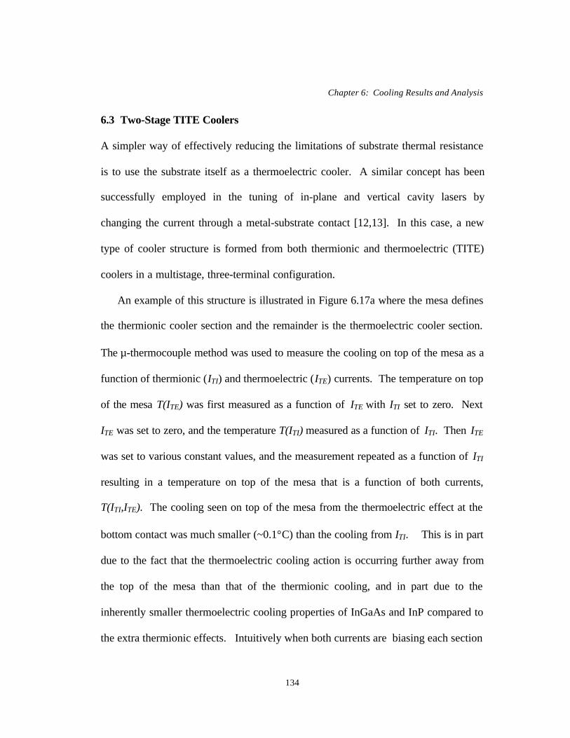
Chapter 6: Cooling Results and Analysis
134
6.3 Two-Stage TITE Coolers
A simpler way of effectively reducing the limitations of substrate thermal resistance
is to use the substrate itself as a thermoelectric cooler. A similar concept has been
successfully employed in the tuning of in-plane and vertical cavity lasers by
changing the current through a metal-substrate contact [12,13]. In this case, a new
type of cooler structure is formed from both thermionic and thermoelectric (TITE)
coolers in a multistage, three-terminal configuration.
An example of this structure is illustrated in Figure 6.17a where the mesa defines
the thermionic cooler section and the remainder is the thermoelectric cooler section.
The µ-thermocouple method was used to measure the cooling on top of the mesa as a
function of thermionic (ITI) and thermoelectric (ITE) currents. The temperature on top
of the mesa T(ITE) was first measured as a function of ITE with ITI set to zero. Next
ITE was set to zero, and the temperature T(ITI) measured as a function of ITI. Then ITE
was set to various constant values, and the measurement repeated as a function of ITI
resulting in a temperature on top of the mesa that is a function of both currents,
T(ITI,ITE). The cooling seen on top of the mesa from the thermoelectric effect at the
bottom contact was much smaller (~0.1°C) than the cooling from ITI. This is in part
due to the fact that the thermoelectric cooling action is occurring further away from
the top of the mesa than that of the thermionic cooling, and in part due to the
inherently smaller thermoelectric cooling properties of InGaAs and InP compared to
the extra thermionic effects. Intuitively when both currents are biasing each section

Chapter 6: Cooling Results and Analysis
135
Backside Metal
InGaAs / InP SL
n+ InGaAs
Thermionic cooler current
Thermoelectric cooler current
ITE ITIn+ InGaAs
n-InP
-0.2
-0.1
0
0.1
0.2
0.3
0.4
0.5
0.6
0 50 100 150 200 250
ITI (mA)
∆T
(K)
Figure 6.17 (a) TITE device structure and geometry. (b) Cooling versus thermionic cooler currentfor three different thermoelectric currents, and (c) the corresponding linear and quadratic coefficientsversus thermoelectric current.
0.004
0.006
0.008
0.01
0.012
0.014
3.4 10-5
3.5 10-5
3.6 10-5
3.7 10-5
3.8 10-5
3.9 10-5
4 10-5
4.1 10-5
-600 -400 -200 0 200 400 600
ITE (mA)
Line
ar (K
/mA
)Q
uadratic (K/m
A2)
ITE = 100 mAITE = 0ITE = -100 mA
(a)
(b)
(c)

Chapter 6: Cooling Results and Analysis
136
of the multistage cooler, it is expected that the resulting temperature, T(ITI,ITE),
would be the sum of the two independent measurements, T(ITI) + T(ITE), however
this is not the case. Figure 6.17b illustrates this point graphically by plotting the
cooling on top of the thermionic cooler for constant thermoelectric currents of 100
mA, 0 mA, and -100 mA. If superposition applied, then the three curves would look
identical with only a vertical shift due to the constant thermoelectric current. This is
obviously not the case as any two curves cross each other at some observable point.
Figure 6.17c plots the corresponding linear and quadratic fitting coefficients versus
ITE, and shows that while the heating coefficient remains approximately constant, the
linear coefficient is changing linearly with thermoelectric current. Therefore, the
constant thermoelectric current not only adds or subtracts a constant amount of
cooling, but it also changes the magnitude of the overall cooling term. The reason
for this ITE-dependent linear coefficient is due to both ITI and ITE superimposing in
the substrate region. If the substrate region has a heating coefficient Ηsub, then the
quadratic term in that region is multiplied by the square of the sum of the currents
flowing through it, Ηsub(ITI + ITE)2. Expanding this expression yields the normal
heating terms, ΗsubITI2, ΗsubITE
2, and a cross term 2ΗsubITEITI. This cross term can be
used to further enhance the overall cooling of this two-stage device. From the slope
of the linear coefficient in Figure 6.17c, Ηsub is measured to be 4.57×10⁻⁶ K/mA2,
which corresponds to only 12% of the total quadratic coefficient measured. This
result is expected since it is believed that most of the heating is caused by the contact

Chapter 6: Cooling Results and Analysis
137
resistance of the metal-semiconductor contacts and from the current carrying wire
bonds. An interesting result of this cross term is that it originates from the heating
effects in the substrate. Therefore even with no additional cooling from the
thermoelectric stage, there exist optimum currents ITI and ITE for which the cooling is
maximized.
6.4 Device Simulation
In the previous analyses of experimental results, an approximate expression
(Equation 6.1) was used to understand the device behavior. In many cases this
simple model made use of values calculated by much more complex three-
dimensional simulations. This section first looks at these finite-element 3-D
simulations [14] that self-consistently solve for the electrical and thermal current
flow. Figure 6.18 shows an SEM photo next to the simulated structure. The 3-D
analysis is necessary to accurately model the electrical and thermal spreading
resistance, however simulation of 3-D structures is somewhat slow. The 3-D
electrical and thermal resistances can be determined for various geometries and used
in an effective 1-D model to obtain faster results when several parameters are to be
varied. The complete model is much more elaborate than the previous one, and can
be used to accurately fit experimental results over wide variations in parameters.
Finally, reliable predictions of improved performance for optimized structures can be
made.
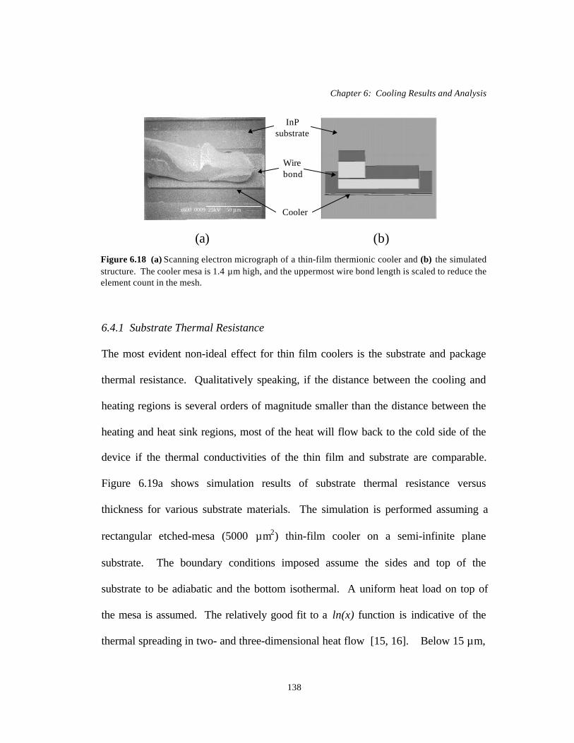
Chapter 6: Cooling Results and Analysis
138
6.4.1 Substrate Thermal Resistance
The most evident non-ideal effect for thin film coolers is the substrate and package
thermal resistance. Qualitatively speaking, if the distance between the cooling and
heating regions is several orders of magnitude smaller than the distance between the
heating and heat sink regions, most of the heat will flow back to the cold side of the
device if the thermal conductivities of the thin film and substrate are comparable.
Figure 6.19a shows simulation results of substrate thermal resistance versus
thickness for various substrate materials. The simulation is performed assuming a
rectangular etched-mesa (5000 µm2) thin-film cooler on a semi-infinite plane
substrate. The boundary conditions imposed assume the sides and top of the
substrate to be adiabatic and the bottom isothermal. A uniform heat load on top of
the mesa is assumed. The relatively good fit to a ln(x) function is indicative of the
thermal spreading in two- and three-dimensional heat flow [15, 16]. Below 15 µm,
InPsubstrate
Cooler
Wirebond
(a) (b)
x600 0009 25kV 50 µm
Figure 6.18 (a) Scanning electron micrograph of a thin-film thermionic cooler and (b) the simulatedstructure. The cooler mesa is 1.4 µm high, and the uppermost wire bond length is scaled to reduce theelement count in the mesh.
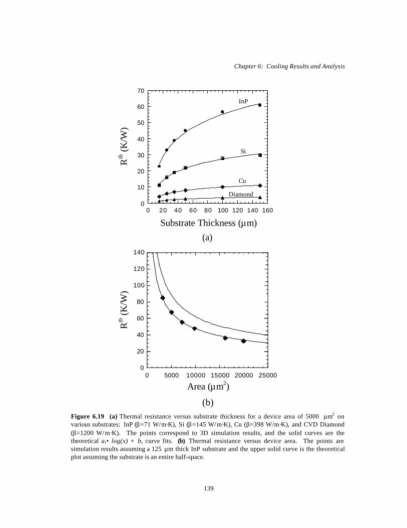
Chapter 6: Cooling Results and Analysis
139
(a)
Substrate Thickness (µm)
Rth (K
/W)
0
10
20
30
40
50
60
70
0 20 40 60 80 100 120 140 160
Si
InP
Cu
Diamond
Area (µm2)
(b)
0
20
40
60
80
100
120
140
0 5000 10000 15000 20000 25000
Rth (K
/W)
Figure 6.19 (a) Thermal resistance versus substrate thickness for a device area of 5000 µm2 onvarious substrates: InP (β=71 W/m·K), Si (β=145 W/m·K), Cu (β=398 W/m·K), and CVD Diamond(β=1200 W/m·K). The points correspond to 3D simulation results, and the solid curves are thetheoretical ai• log(x) + bi curve fits. (b) Thermal resistance versus device area. The points aresimulation results assuming a 125 µm thick InP substrate and the upper solid curve is the theoreticalplot assuming the substrate is an entire half-space.

Chapter 6: Cooling Results and Analysis
140
the heat flow becomes dominantly one-dimensional and the thermal resistance scales
linearly with substrate thickness. The logarithmic fitting function of the thermal
resistance and the corresponding coefficients can be given as,
where Rthermal has units of [K/W], h is the substrate thickness in microns, and ai & bi
are the fitting coefficients corresponding to the thermal conductivity of the substrate
(β i).
Clearly it is beneficial to use substrates with high thermal conductivity and a
minimum thickness. However, thin film coolers that are grown on typical substrate
materials (InP, Si, etc.) can be lapped only by a limited amount before the material
begins to warp and become severely fragile. This warping occurs with InP substrates
when they are lapped below 100 µm, which for the device size simulated
corresponds to a thermal resistance of 57 K/W. Using a 1 µm film of InGaAsP for
the cooler (β =3.3 W/m·K) gives a thermal resistance of 61.6 K/W showing that
roughly half the heat flows back to the cold side of the device.
The area of the device also affects the thermal resistance. Figure 6.19b shows
simulation results of thermal resistance (points on lower curve) for various device
areas assuming a 125-µm-thick InP substrate. The upper curve represents a
;
iithermal bhahR += )ln()(
]/[1167
mKWa
ii β
=]/[
1445mKW
bi
i β−
=
(6.7a)
(6.7b)

Chapter 6: Cooling Results and Analysis
141
theoretical expression that assumes a disk heat source on a half-space denoting a
purely three-dimensional heat flow,
where β is the thermal conductivity of the half space, and A is the area of the disk
[15]. The simulation results are fitted with this same expression (solid line), and the
resulting expression is equivalent to Equation 6.8 multiplied by a reduction factor of
0.761. As the substrate thickness is increased, the simulation results approach that of
the theoretical expression.
6.4.2 Complete Device Simulation
Simulation of complete 3-D device structures with all non-ideal effects included can
be used to fit experimental data and determine which areas of the thin film cooler
design need to be improved. These simulations model self-consistently the thermal
and electrical operation. Once the simulation is in agreement with experimentally
measured temperature profiles, particular non-ideal effects can be removed in
succession and the dominating ones determined.
Measured cooling for a 1-µm-thick InGaAs/InGaAsP superlattice (50×100 µm2)
is shown with the simulated curve in Figure 6.20 (curve 1). Both the thermionic and
thermoelectric cooling effects were included in the simulation and the thermal
conductivity of the superlattice was taken to be 5 W/m⋅K. With an accurate model of
AR thermal β
π4
= (6.8)

Chapter 6: Cooling Results and Analysis
142
the device in hand, the contact resistance was set to zero and the simulation was
repeated (curve 2). The maximum cooling temperature increased from 1.14 to 2.3 K.
This was repeated with the contact resistance reset to its original value and the 120-
µm-thick InP substrate replaced with a 10 µm copper substrate resulting in a similar
improvement in performance (curve 3). The simulation was then again performed
with the top wire bond removed (not shown), resulting only in a very small increase
in cooling. Finally, the simulation was repeated once more with both the contact
resistance removed and the copper substrate resulting in a maximum cooling
temperature of 6.07 K and a cooling power density of 1821 W/cm2 (curve 4).
1
2
3
4
5
6
7
10 100 1000 104
12 3
4
Figure 6.20 Experimental and simulation results for a 1µm thick InGaAs/InGaAsP superlatticecooler. The points and curve 1 correspond to the simulated fit of the experimental data with all non-ideal effects. Curves 2 and 3 are the repeated simulation results when the contact resistance andsubstrate thermal resistance are taken away respectively. Curve 4 corresponds to both non-idealeffects removed.
I (mA)
∆T
(K)

Chapter 6: Cooling Results and Analysis
143
Therefore in this particular device structure, both the contact resistance and the
substrate thermal resistance will need to be reduced to see substantial improvement
in performance.
It is insightful to examine the temperature and voltage profiles along a path
through the 3-D structure. Figure 6.21 shows simulation results following a line
from the bottom of the substrate, traveling through the cooler, and continuing to the
end of the wire bond. The current source is applied between the end of the wire
bond and the bottom substrate plane, and an ideal heat sink is assumed at these two
points. The wire bond (25µm diameter) was 400 µm long, but was scaled by a factor
-1
-0.5
0
0.5
1
0
0.01
0.02
0.03
0.04
0.05
0 50 100 150
Position (µm)
Tem
pera
ture
(K) V
oltage (V)
substratewire
cooler
Figure 6.21 Simulated temperature and voltage profiles along a path through the substrate, cooler,and wire bond. The actual wire bond length was 400 µm, but was scaled by 20× to reduce thenumber of elements in the 3-D simulation.
Chapter 6: Cooling Results and Analysis
144
of twenty to reduce the number of elements in the 3-D simulation. This kind of
scaling can only be done in regions that are purely 1-D, such as the long narrow Au-
wire. A linear voltage drop and quadratic temperature distribution is observed along
the wire bond as expected for 1-D behavior. At the cooler, a steep temperature
gradient is observed across the 1-µm-thick film indicating a large heat flux. There is
also a sharp voltage drop located at the interface of the metal and semiconductor
corresponding to the contact resistance which was assumed to be 6×10⁻⁷ Ω cm2. This
voltage drop is nearly one quarter the total voltage across the entire structure. Inside
the substrate the voltage and temperature profiles can be seen to drop off non-
linearly due to the three-dimensional spreading. Finally, near the bottom of the
substrate there is another change in the slope due to a 4-µm-thick Sn solder layer.
From the 3-D modeling, it is possible to extract the important thermal and
electrical spreading resistances similar to Figure 6.19. Using these simulated values
it becomes possible to construct an accurate 1-D model. Figure 6.22 shows the
updated 1-D circuit diagram model with the appropriate cooling and heating loads, as
well as boundary conditions. In each homogeneous region x, the heat flux equation
can be applied,
xxxx A
Idx
TdA
σβ
2
2
2 −= (6.9)

Chapter 6: Cooling Results and Analysis
145
which relates the temperature gradient to the Joule heat generation where σx, βx, and
Ax, are the electrical conductivity, thermal conductivity, and area respectively.
Taking Equation 6.9 and integrating twice with respect to position, an expression for
temperature with two unknown constants results.
For three regions this gives a total of six unknowns. Four boundary conditions exist
for the temperature since it must be continuous across all three regions. Here
thermal boundary resistances are neglected. The last two boundary conditions are
obtained from the discontinuity of the heat conduction (βA⋅dT/dx) by the heat
generation and absorption on either side of the cooler, resulting in six boundary
xxxxx
CxBxA
IxT ++
−= 2
2
2
2)(
βσ(6.10)
Figure 6.22 Updated 1-D model showing cooling (←•) and heating (→•) flux, as well as boundaryconditions shown by the blocks. The resistors Rn represent both electrical and thermal resistances.Qs, Qd, Qc, and Qw refer to the Joule heating in the substrate, device, contact, and wire bondrespectively. QTI is the thermionic heating/cooling, QTE1 the thermoelectric cooling at the metal-semiconductor interface, and QTE2 the thermoelectric cooling at the InGaAs-InP substrate interface.Not shown is the thermocouple heat load.
QTI + QTE1Rw
Rd
Rs
QTI
Qs
QTE2
Qd
Qc
Qw

Chapter 6: Cooling Results and Analysis
146
conditions and six unknowns. The solution was then manipulated and plotted in
MATLAB [17].
Figure 6.23 compares the results of the 3-D and 1-D models. The two
simulations were found to be in good agreement over various changes in parameters.
The largest difference can be seen in the temperature profile through the substrate
where the 1-D and 3-D distributions are inherently different. The other minor
discrepancy is in the temperature distribution of the wire that arises from the
additional thermal spreading at the wire-cooler interface. This effect is more
difficult to include in the 1-D model.
-1.5
-1
-0.5
0
0.5
1
1.5
0 50 100 150
MATLABANSYS
wire
cooler
substrate
Figure 6.23 Comparison of simulated temperature profiles through the substrate, cooler, and wirebond for the three-dimensional (ANSYS) and one-dimensional (MATLAB) models. The zerotemperature axis is relative to 300 K.
Position (µm)
Tem
pera
ture
(K)

Chapter 6: Cooling Results and Analysis
147
Using this 1-D model, it has been possible to closely match the area dependence
of cooling seen experimentally with the simulation. Figure 6.24 shows an example
of measured and simulated cooling versus current for several different device sizes
and heat sink temperatures of an InGaAs/InGaAsP p-type superlattice cooler. These
simulations also used a more intricate model for the integrated side contact.
Excellent agreement can be seen between the two results, and even the change in
optimum device size over heat sink temperature from 150×150 µm2 to 100×100 µm2
was reproduced by the simulation. The temperature dependence of optimum device
size stems from the area dependence of thermal conduction through the SL and
increased cooling due to the larger energy spread of the carriers. From the
simulation, the limiting factors on cooler performance could be determined. Contact
resistance and the wire contact were determined to be of greatest concern with a
lesser limitation from the substrate thermal resistance. Figure 6.25 shows simulation
predictions for minimized side-contact losses and reduced contact resistance (5×10⁻⁷
Ωcm2). Nearly 10 K at room temperature should be possible, corresponding to
cooling power densities exceeding 1000 W/cm2.
The advantage of the 1-D model is the speed with which many device
parameters can be varied and their affects determined. Figure 6.26a shows a
simulation of maximum cooling versus contact resistivity for various cooler
thicknesses. To observe just the limitation of contact resistance, the other non-ideal
effects were minimized to reasonable values. The substrate thermal resistance was
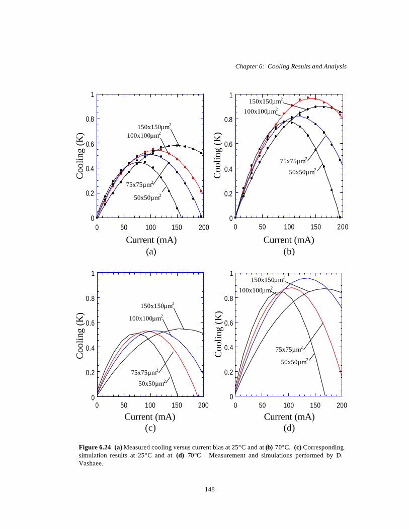
Chapter 6: Cooling Results and Analysis
148
0
0.2
0.4
0.6
0.8
1
0 50 100 150 2000
0.2
0.4
0.6
0.8
1
0 50 100 150 200
0
0.2
0.4
0.6
0.8
1
0 50 100 150 2000
0.2
0.4
0.6
0.8
1
0 50 100 150 200
(a) (b)
(c) (d)
Current (mA) Current (mA)
Current (mA) Current (mA)
Coo
ling
(K)
Coo
ling
(K)
Coo
ling
(K)
Coo
ling
(K)
Figure 6.24 (a) Measured cooling versus current bias at 25°C and at (b) 70°C. (c) Correspondingsimulation results at 25°C and at (d) 70°C. Measurement and simulations performed by D.Vashaee.
150x150µm2
100x100µm2
75x75µm2
50x50µm2
150x150µm2
100x100µm2
75x75µm2
50x50µm2
150x150µm2
100x100µm2
75x75µm2
50x50µm2
150x150µm2
100x100µm2
75x75µm2
50x50µm2
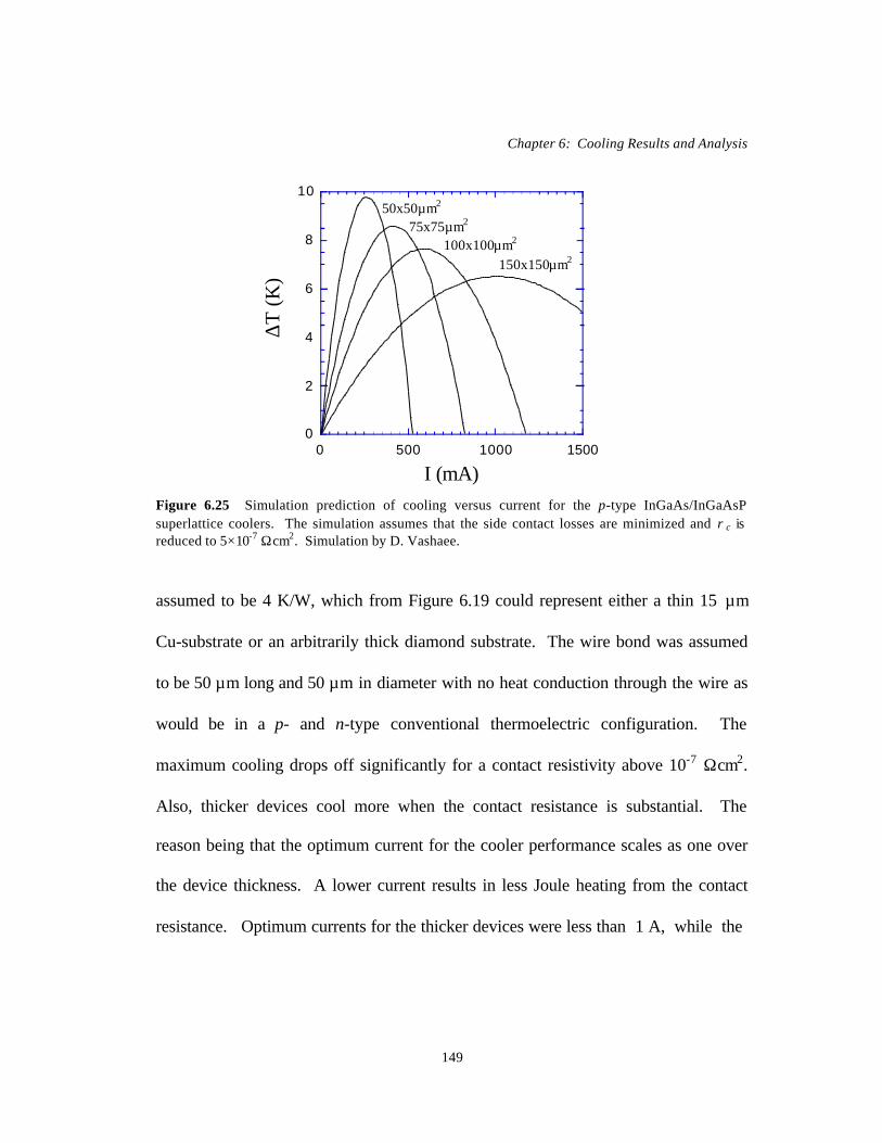
Chapter 6: Cooling Results and Analysis
149
assumed to be 4 K/W, which from Figure 6.19 could represent either a thin 15 µm
Cu-substrate or an arbitrarily thick diamond substrate. The wire bond was assumed
to be 50 µm long and 50 µm in diameter with no heat conduction through the wire as
would be in a p- and n-type conventional thermoelectric configuration. The
maximum cooling drops off significantly for a contact resistivity above 10-7 Ωcm2.
Also, thicker devices cool more when the contact resistance is substantial. The
reason being that the optimum current for the cooler performance scales as one over
the device thickness. A lower current results in less Joule heating from the contact
resistance. Optimum currents for the thicker devices were less than 1 A, while the
0
2
4
6
8
10
0 500 1000 1500
Figure 6.25 Simulation prediction of cooling versus current for the p-type InGaAs/InGaAsPsuperlattice coolers. The simulation assumes that the side contact losses are minimized and ρc isreduced to 5×10⁻⁷ Ωcm2. Simulation by D. Vashaee.
I (mA)
∆T
(K)
150x150µm2100x100µm2
75x75µm250x50µm2
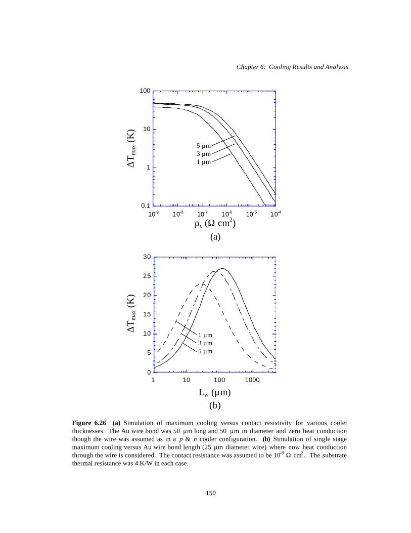
Chapter 6: Cooling Results and Analysis
150
0.1
1
10
100
10-9 10-8 10-7 10-6 10-5 10-4
ρc (Ω cm2)
∆T
max
(K)
Figure 6.26 (a) Simulation of maximum cooling versus contact resistivity for various coolerthicknesses. The Au wire bond was 50 µm long and 50 µm in diameter and zero heat conductionthough the wire was assumed as in a p & n cooler configuration. (b) Simulation of single stagemaximum cooling versus Au wire bond length (25 µm diameter wire) where now heat conductionthrough the wire is considered. The contact resistance was assumed to be 10-8 Ω cm2. The substratethermal resistance was 4 K/W in each case.
5 µm3 µm1 µm
0
5
10
15
20
25
30
1 10 100 1000
(a)
Lw (µm)
∆T
max
(K)
(b)
1 µm3 µm5 µm
Chapter 6: Cooling Results and Analysis
151
thinner devices required as much as 5 A. The thicker devices do attain higher
absolute cooling in this case, but the cooling power remains approximately
unchanged.
In applications for which single element coolers are monolithically integrated
with electronic or optoelectronic devices, it is necessary to have an external wire
bond connected directly to the cold side of the cooler. The question arises as to
whether useful cooling can still be achieved in this configuration. Figure 6.26b
shows a simulation of maximum cooling versus wire bond length (25µm diameter).
In this case heat conduction through the wire is considered, and the contact
resistivity is assumed to be 10-8 Ωcm2 in order to study the effects of the wire only.
For a given cooler thickness, there exists an optimum wire length resulting from a
trade-off between Joule heating in long wires and heat conduction from heat sink to
the cold junction in short wires. At longer wire lengths the thicker devices cool
better by the same argument made for contact resistance. That is thicker coolers are
optimized at a lower current and hence less Joule heating occurs. The cooling power
of the thicker devices is somewhat reduced however. For shorter wire lengths the
thinner cooler performs best. Since the thinner cooler has a smaller thermal
resistance between cold and hot junctions, more heat conduction occurs across the
cooler than through the wire.
The temperature dependence of material properties and cooling amount are not
taken into account in the above models. For small values of cooling and heating on

Chapter 6: Cooling Results and Analysis
152
Figure 6.27 (a) Thermal image from a 3-D ANSYS simulation of a rectangular shaped (50×100µm2)thin-film cooler. The tall block structure at the far end of the cooler is the scaled wire bond. (b) Topview of the simulated thermal contours on the surface of the cooler. (c) Optical normalization imageof a square (40×40µm2) cooler with integrated wire bond and (d) the thermal image from athermoreflectance measurement. Both the simulation and measurement show a similar profile on topof the cooler due to the Joule heating and heat conduction from the wire bond. The image is notcorrected for the different thermoreflectance coefficient of the InP surface. Only values on top of thecooler are valid. Bottom images from J. Christofferson.
(c) (d)
(a) (b)
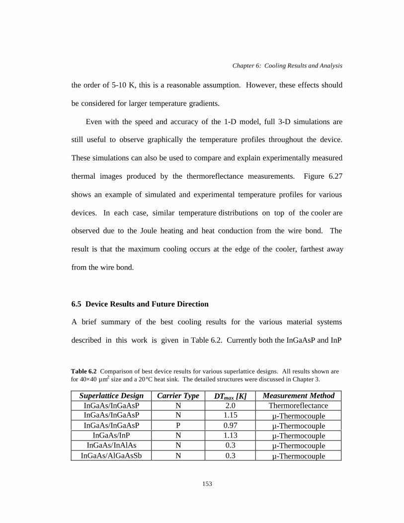
Chapter 6: Cooling Results and Analysis
153
the order of 5-10 K, this is a reasonable assumption. However, these effects should
be considered for larger temperature gradients.
Even with the speed and accuracy of the 1-D model, full 3-D simulations are
still useful to observe graphically the temperature profiles throughout the device.
These simulations can also be used to compare and explain experimentally measured
thermal images produced by the thermoreflectance measurements. Figure 6.27
shows an example of simulated and experimental temperature profiles for various
devices. In each case, similar temperature distributions on top of the cooler are
observed due to the Joule heating and heat conduction from the wire bond. The
result is that the maximum cooling occurs at the edge of the cooler, farthest away
from the wire bond.
6.5 Device Results and Future Direction
A brief summary of the best cooling results for the various material systems
described in this work is given in Table 6.2. Currently both the InGaAsP and InP
Superlattice Design Carrier Type ∆Tmax [K] Measurement MethodInGaAs/InGaAsP N 2.0 ThermoreflectanceInGaAs/InGaAsP N 1.15 µ-ThermocoupleInGaAs/InGaAsP P 0.97 µ-Thermocouple
InGaAs/InP N 1.13 µ-ThermocoupleInGaAs/InAlAs N 0.3 µ-Thermocouple
InGaAs/AlGaAsSb N 0.3 µ-Thermocouple
Table 6.2 Comparison of best device results for various superlattice designs. All results shown arefor 40×40 µm2 size and a 20°C heat sink. The detailed structures were discussed in Chapter 3.

Chapter 6: Cooling Results and Analysis
154
barrier n-type devices show the greatest amount of cooling, however the InP-barrier
devices possess greater potential as shown theoretically in Chapter 2. Continued
work in optimizing the designs to prevent mini-band conduction should allow these
devices to realize this predicted potential. While the InAlAs-barrier devices carry
even greater prospects, more work is necessary to fully understand the design issues
in such highly doped structures, especially in avoiding the mini-band conduction that
is more prevalent in these high-barrier short-period superlattices. Sb-based devices
are also a good direction to pursue due to their good thermoelectric properties and
capability to tailor the barrier heights over a wide range, yet much work is necessary
in studying the material issues since this is not a well known material system.
Besides the n-type devices, the p-type InGaAs/InGaAsP structure also performed
relatively well. The biggest inhibitor was the high contact resistance which limited
the allowable current bias. Reducing the p-type InGaAs contact-resistance should
immediately result in cooling values of 10K as predicted in Figure 6.25. Moreover,
the p-type material boasts a much greater Seebeck coefficient than that of its n-type
counterpart as shown in Chapter 4.
6.6 Summary
Numerous practical and effective methods for accurately characterizing temperature
over small spatial dimensions have been developed. The most expeditious technique
for point measurements has been the µ-thermocouple system, but its heat load effects

Chapter 6: Cooling Results and Analysis
155
on small devices must be considered. The foremost method for thermal imaging
measurements has been the thermoreflectance system which has far outperformed
infrared-based cameras.
A thorough experimental investigation of InP-based thin-film thermionic coolers
has been presented. Through modeling of the geometry and temperature dependent
cooling, an understanding of device performance has been achieved. Evidence exists
to suggest thermionic emission is a significant portion of cooling in some structures,
but it has been difficult to quantify. Important parameters and non-ideal effects in
thin-film coolers have been discussed through experimental and simulation results.
A three-dimensional finite element simulation has been developed and used to
determine the dominating non-ideal mechanisms for thin film coolers and the impact
of changing device characteristics. A one-dimensional simulation was also
developed using three-dimensional spreading resistance values obtained from the
three-dimensional model. Contact resistance, finite thermal resistance of substrate
and heat sink, and heat generation in wire bonds have all been identified as
limitations in thin-film cooler performance. Experimental results in thin-film
thermionic emission coolers have demonstrated cooling by 1-2 K at room
temperature, and even larger values at elevated heat sink temperatures. This amount
of cooling over 1-2 µm thick barriers corresponds to cooling power densities up to
1000 W/cm2. Simulations have predicted cooling of 20-30 degrees with cooling

Chapter 6: Cooling Results and Analysis
156
power densities of many 1000’s W/cm2 for more optimized structures and
packaging.
A new type of cooler structure was also discussed, the two-stage three-terminal
TITE cooler. Enhanced cooling was demonstrated with an InP-based TITE structure,
and the interesting three-terminal effects studied. It is expected that this new design
will have greater consequence for more optimally doped InP substrates, or with a
different material system for which the substrate possesses better thermoelectric
properties.
REFERENCES
1. LabVIEW Release 5.1 (1999) by National Instruments, Austin, TX.
2. J.M. Swartz, J.R. Gaines, “Wide range thermometry using gallium arsenide sensors,”Measurement & Control in Science & Industry, Vol. 4, 1972.
3. H. Wang, M. Bartkowiak, F.A. Modine, R.B. Dinwiddie, L.A. Boatner, G.D. Mahan,“Nonuniform Heating in Zinc Oxide Varistors Studied by Infrared Imaging and ComputerSimulation,” J. Am. Ceram. Soc., Vol. 81, No.8, 1998, p.2013-22.
4. A.D. Oliver, K.D. Wise, “A 1024-element bulk-micromachined thermopile infrared imagingarray for semiconductor process control,” Sensors and Actuators A, Vol.A73, No.3, 1999, p.222-31.
5. In Collaboration with the High Temperature Materials Laboratory at Oak Ridge NationalLaboratories, Oak Ridge, TN. The system was developed by H. Wang and C. Hubbard, directedby A. Pasto.
6. Y.S. Ju, K.E. Goodson, “Short-time-scale thermal mapping of microdevices using a scanningthermoreflectance technique,” Trans. Of the ASME, May 1998, p.306-13.
7. T. Phan, S. Dilhaire, V. Quintard, W. Claeys, J. Batsale, “Thermoreflectance measurements oftransient temperature upon integrated circuits: application to thermal conductivity identification,”Microelectronics Journal, Vol. 29, 1998, p.181-90.
8. A. Mansanares, D. Fournier, A. Boccara, “Temperature measurements of telecommunicationlasers on a micrometre scale,” Elec. Lett., Vol. 29, No.23, 1993, p.2045-7.

Chapter 6: Cooling Results and Analysis
157
9. D.M. Rowe, CRC Handbook of Thermoelectrics, CRC, New York, 1995.
10. S.T. Huxtable, A. Shakouri, C. LaBounty, X. Fan, P. Abraham, Y.J. Chiu, J.E. Bowers, A.Majumdar, “Thermal Conductivity of Indium Phosphide-Based Superlattices,” MicroscaleThermophysical Engineering , Vol.4, 2000, p.197-203.
11. C. LaBounty, G. Almuneau, A. Shakouri, J.E. Bowers, "Sb-based III-V Cooler," 19th
International Conference on Thermoelectrics, Cardiff, Wales, August 2000.
12. N.K. Dutta, R.L. Cella, R.L. Brown, D.T.C. Huo, “Monolithically integrated thermoelectriccontrolled laser diode,” Appl. Phys. Lett., Vol. 47, No.3, 1985, pp. 222-4.
13. P.R. Berger, N.K. Dutta, K.D. Choquette, G. Hasnain, N. Chand, “Monolithically Peltier-cooledvertical-cavity surface-emitting lasers,” Appl. Phys. Lett., Vol. 59, No.1, 1991, pp. 117-9.
14. ANSYS Release 5.5.3 (1999) by Swanson Analysis Systems, Inc., Houston, PA.
15. L. Coldren, S. Corzine, Diode Lasers and Photonic Integrated Circuits, John Wiley & Sons, Inc.,New York, 1995.
16. F. Masana, “A Closed Form Solution of Junction to Substrate Thermal Resistance inSemiconductor Chips,” IEEE Trans-CPMT-A, Vol. 19, No.4, 1996, pp. 539-45.
17. MATLAB Release 5.0.0.4073 (1996) by The MathWorks, Inc.

Chapter 6: Cooling Results and Analysis
158

Chapter 7: Integration with Optoelectronic Devices
159
Chapter 7
Integration with Optoelectronic Devices
With the thorough discussion of single-stage micro-coolers and related issues
presented in previous chapters, we can now turn our attention to integration with
optoelectronic devices. Most optoelectronic devices can benefit from some form of
cooling or temperature stabilization and for many applications of these devices, such
as wavelength division multiplexed (WDM) optical communication systems, it is
essential.
While large temperature differences are not yet available with thin-film coolers,
they can currently provide very precise localized cooling and heating. They can also
provide large cooling or heating power densities, orders of magnitude more than
conventional thermoelectric devices. Figure 7.1 shows an example of this
microscale temperature control on three patterned coolers with a lateral spacing of 20
µm. Approximately 4 K of temperature differential is seen with no noticeable
change in the surrounding surfaces. This temperature change corresponds to 100’s
of W/cm2 in cooling or heating power density.
In this chapter, we will first investigate the frequency response of cooling as this
is an important parameter in the applications discussed later. Three examples of
integrated cooling are then described, which include a p-i-n photodiode, in-plane
laser, and VCSEL structure. Different approaches are utilized for each case, which
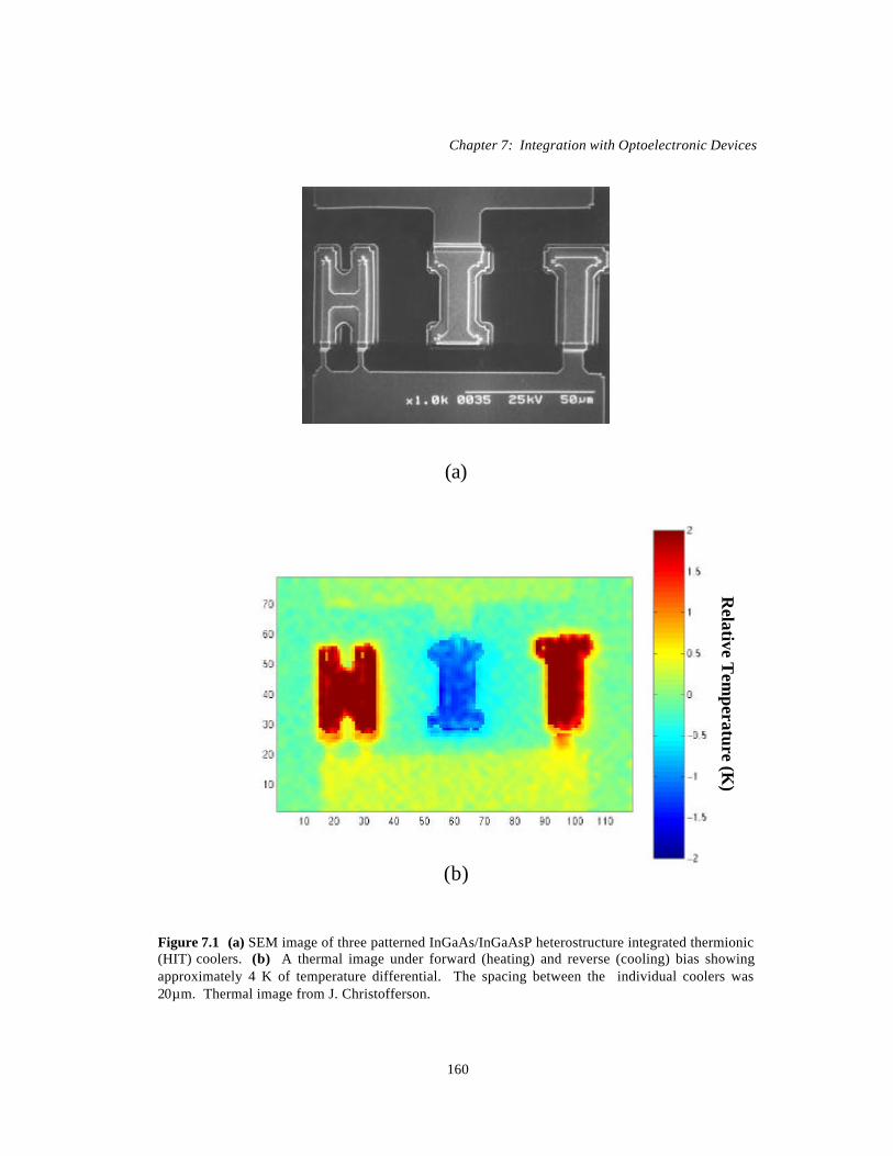
Chapter 7: Integration with Optoelectronic Devices
160
Relative T
emperature (K
)
Figure 7.1 (a) SEM image of three patterned InGaAs/InGaAsP heterostructure integrated thermionic(HIT) coolers. (b) A thermal image under forward (heating) and reverse (cooling) bias showingapproximately 4 K of temperature differential. The spacing between the individual coolers was20µm. Thermal image from J. Christofferson.
(a)
(b)

Chapter 7: Integration with Optoelectronic Devices
161
can be categorized as monolithic or heterogeneous integration. Thermionic cooling
in heterostructures is shown to match well with the requirements for monolithic
integration since the coolers themselves are made from the same materials allowing
for lattice-matched structures. While this may still involve a compromise in the
optimum design of each structure, the processing is much easier. Heterogeneous
integration offers more flexibility as each device is separately optimized and joined
afterwards. This can require more complicated packaging as proper alignment is
needed and possibly windows for light propagation. Also, a careful choice of joining
materials must be made so that a good thermal contact is established.
7.1 Transient Operation
In many applications, the speed with which cooling occurs is an important
parameter. In thermally tuned devices, the operating characteristics may only be
changed as fast as the temperature dictates, as in the wavelength of a laser for
instance. The thermal diffusion time can be expressed in terms of the characteristic
length L and thermal diffusivity α:
Since the cooling region of integrated thin-film cooler structures can be located so
closely to the integrated device (~ several µm), the intrinsic diffusion time can be
sub-microsecond. Comparatively, cooling a device through the substrate as in
ατ
2L= (7.1)
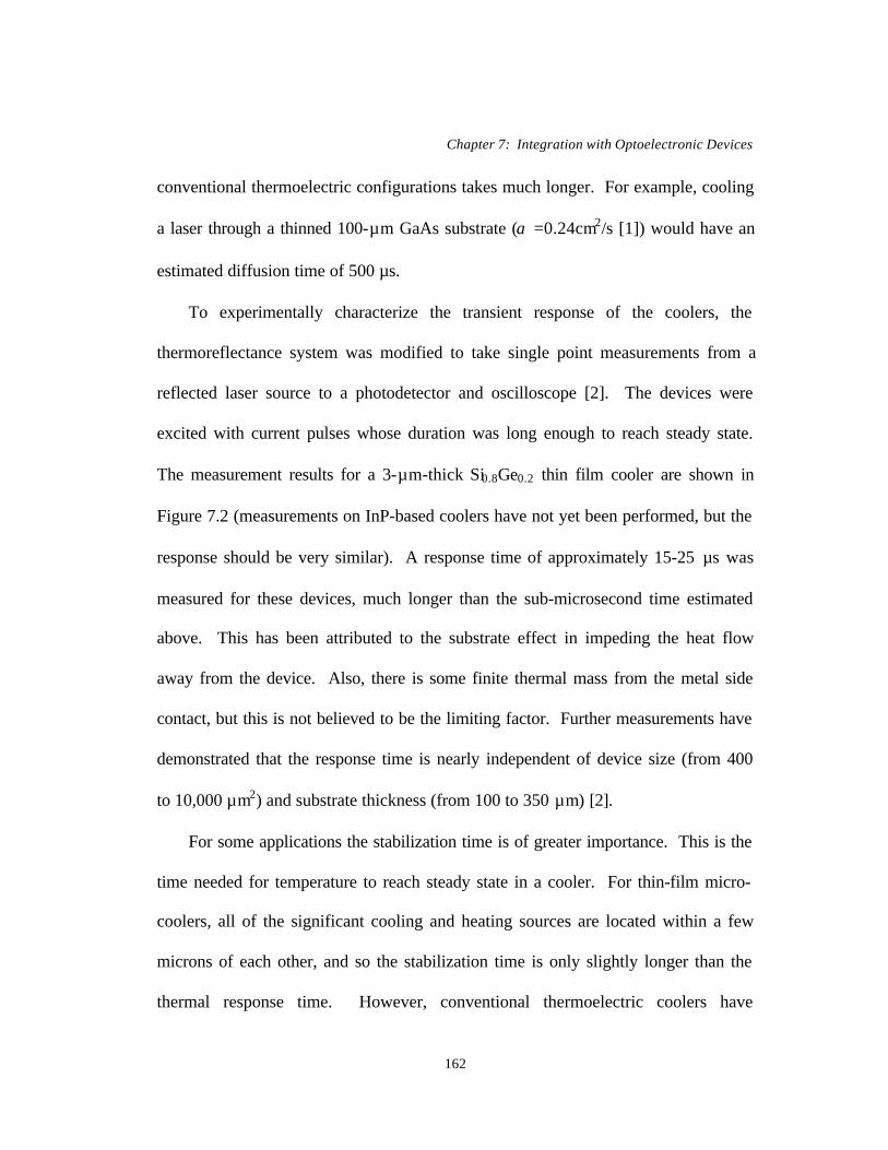
Chapter 7: Integration with Optoelectronic Devices
162
conventional thermoelectric configurations takes much longer. For example, cooling
a laser through a thinned 100-µm GaAs substrate (α =0.24cm2/s [1]) would have an
estimated diffusion time of 500 µs.
To experimentally characterize the transient response of the coolers, the
thermoreflectance system was modified to take single point measurements from a
reflected laser source to a photodetector and oscilloscope [2]. The devices were
excited with current pulses whose duration was long enough to reach steady state.
The measurement results for a 3-µm-thick Si0.8Ge0.2 thin film cooler are shown in
Figure 7.2 (measurements on InP-based coolers have not yet been performed, but the
response should be very similar). A response time of approximately 15-25 µs was
measured for these devices, much longer than the sub-microsecond time estimated
above. This has been attributed to the substrate effect in impeding the heat flow
away from the device. Also, there is some finite thermal mass from the metal side
contact, but this is not believed to be the limiting factor. Further measurements have
demonstrated that the response time is nearly independent of device size (from 400
to 10,000 µm2) and substrate thickness (from 100 to 350 µm) [2].
For some applications the stabilization time is of greater importance. This is the
time needed for temperature to reach steady state in a cooler. For thin-film micro-
coolers, all of the significant cooling and heating sources are located within a few
microns of each other, and so the stabilization time is only slightly longer than the
thermal response time. However, conventional thermoelectric coolers have

Chapter 7: Integration with Optoelectronic Devices
163
thermoelement lengths of several millimeters resulting in stabilization times of 20 to
30 seconds [3].
In some instances, the cooling requirements are constantly changing, and the
concept of cooling frequency-response can be introduced. In this measurement, the
coolers are driven by a square-pulse current-signal at a given frequency, and the
temperature is measured by the thermoreflectance method. Figure 7.3a shows the
large-signal frequency-response of an 80×80 µm2 3-µm-thick SiGe cooler at various
zero-to-peak currents. For the first set of points at low current (I=200 mA), the Joule
heating effects can be neglected, and the response is simply dependent on the
thermal RC time-constant (τ = 46.3 µs) of the cooling region. As the current is
Coo
ling
(a.u
.)
Time (µs)
Figure 7.2 Transient response of two different sized SiGe thin film coolers as a function of time. Theresponse time is on the order of 15-25 µs. Measured by A. Fitting.
0
0.1
0.2
0.3
0.4
0.5
0.6
0.7
0.8
0 10 20 30 40 50 60
40×40 µm2
80×80 µm2
0.0
-0.2
-0.4
-0.6
-0.8

Chapter 7: Integration with Optoelectronic Devices
164
0
0.5
1
1.5
2
2.5
3
103 104 105
∆T
(K)
Frequency (Hz)
Figure 7.3 (a) Frequency response of an 80×80µm2 3-µm-thick SiGe micro cooler. The variouscurrents (I) indicated are 0 to peak values of the square-pulse input signal. Exponential curve fits areused for the two lowest currents. (b) Frequency response of the normalized cooling and heatingcoefficients of the ∆T versus I curves. Measurements by J. Christofferson.
0.01
0.1
1
103 104 105
Nor
mal
ized
Am
plitu
de
Frequency (Hz)
(a)
(b)
I = 600mA
I = 200mA
I = 1450mA
CoolingCoefficient
HeatingCoefficient

Chapter 7: Integration with Optoelectronic Devices
165
increased and the non-linear heating becomes prevalent, the temperature no longer
follows a simple exponential relation with frequency. This is further complicated by
the higher order harmonic generation from the square-pulse current-waveform.
Interestingly, for current pulse magnitudes that produce no cooling at DC or low
frequencies, cooling can still occur at higher frequencies as shown for the 1450 mA
curve in Figure 7.3a. Looking more closely in Figure 7.3b, the cooling coefficient is
seen to have a faster response than that of the heating coefficient. This can be
attributed to the close proximity and localization of the cooling effects versus the
more spread out and distributed heating effects. More work is necessary to solve the
energy-balance heat-diffusion equations and to accurately simulate the frequency
response to fully understand the behavior.
7.2 PIN Photodiode
For the first demonstration of monolithically integrated cooling with an
optoelectronic device, an InP p-i-n diode was chosen. The tested thermionic cooler
structure consisted of a 1-µm-thick superlattice barrier (low-barrier design from
Chapter 3) surrounded by n+ InGaAs cathode and anode layers grown by metal
organic chemical vapor deposition (MOCVD). The cathode and anode layers were
0.3 µm and 0.5 µm thick, respectively. On top of these layers, the 0.85-µm-thick
p-i-n diode was grown during the same MOCVD growth. In two wet etching steps,
two stacked mesas are defined corresponding to the diode on top of the cooler as

Chapter 7: Integration with Optoelectronic Devices
166
shown in Figure 7.4. The cooler mesas ranged in size from 20×40 µm2 to 100×200
µm2, and the diode size was one half that of the cooler size. Ti/Pt/Au was used to
make ohmic contacts to both the p- and n-type material. The substrate was thinned
to approximately 125 µm before the backside metal was deposited. The integrated
devices were then cleaved, packaged, and wire bonded for testing.
The diode served two purposes in the measurement. First, by changing the
current through the diode we could effectively change the heat load of the cooler.
Second, by monitoring the voltage across the diode, we could measure the
temperature [4] on the cold side of the cooler, TC. The temperature sensitivity of the
diode near room temperature was determined to be 1.936 mV/°C at a bias of 1 mA.
Figure 7.4 SEM of a processed device showing the monolithically integrated p-i-n photodiode on topof the 1-µm-thick InGaAs/InGaAsP thermionic cooler.

Chapter 7: Integration with Optoelectronic Devices
167
The measurement set-up is illustrated in Figure 7.5. A constant current (ID) was sent
through the diode and the diode voltage (VD) was monitored as the cooler current (IC)
was varied. The resistors of Figure 7.5 represent the parasitic wire bonds that add to
the heat load on the device. The measured voltage can be expressed as:
where RD1 and RD2 are the wire bond resistances, ρc is the contact resistivity, and Ac
is the area of the metal contact on the cooler. If Equation 7.2 is rearranged to solve
for VD as a function of IC, then the resulting expression is equal to the measured
voltage minus some constant values, and minus a value that changes with respect to
)()( 21 CDc
cDDDDM II
AVIRRV ++++=
ρ(7.2)
Backside Metal
InGaAs/InGaAsP S.L. n+ InGaAs
ID
IC
p-i-n diode
RCRD2RD1
n-InP
VM
Figure 7.5 Set-up for measuring the temperature of the integrated diode versus the current through thecooler (IC) and the diode (ID). RD1, RD2, and RC are the wire bond resistances.

Chapter 7: Integration with Optoelectronic Devices
168
IC, that is ρcIC /AC. Therefore to correctly measure the temperature on top of the
device, the contact resistivity must be determined. Once VD is known, the
temperature can be calculated using the temperature dependence of the diode voltage
at a constant current given above.
The temperature of the device was also measured with the micro-thermocouple
system. Device A from Figure 7.6 shows the temperature versus current for the cold
side of a 70×140 µm2 cooler that had the integrated diode removed by selective wet
etching. The temperature data was curve fit with a second order polynomial
resulting in a linear coefficient of 3.53 K/A, and a quadratic coefficient of 3.37 K/A2.
Since this cooler structure was identical to the one with the integrated diode (device
B), the two devices should have the same linear coefficient. The quadratic
coefficient, on the other hand, may differ since Joule heating is dependent on
processing variations such as contact resistance, packaging and wire bonding.
Consequently, the contact resistance (ρc) can be determined from Equation 7.2 by
adjusting its value until the linear coefficients match. Using this method, device B
from Figure 7.6 also shows the temperature versus current for the cold side of a
cooler with an integrated diode biased at 1 mA. The performance is much worse due
to poorer packaging and a higher contact resistance. For device B the contact
resistance is at least doubled since the effective contact area is only one-half that of
device A due to the space that is taken by the diode. Its value was determined to be
4.4×10⁻⁶ Ωcm2. Comparatively, the contact resistance for device A was measured by
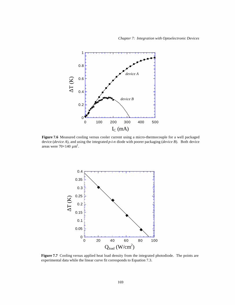
Chapter 7: Integration with Optoelectronic Devices
169
0
0.2
0.4
0.6
0.8
1
0 100 200 300 400 500
∆T
(K)
IC (mA)
device A
device B
Figure 7.6 Measured cooling versus cooler current using a micro-thermocouple for a well packageddevice (device A), and using the integrated p-i-n diode with poorer packaging (device B). Both deviceareas were 70×140 µm2.
∆T
(K)
Qload (W/cm2)Figure 7.7 Cooling versus applied heat load density from the integrated photodiode. The points areexperimental data while the linear curve fit corresponds to Equation 7.3.
0
0.05
0.1
0.15
0.2
0.25
0.3
0.35
0.4
0 20 40 60 80 100
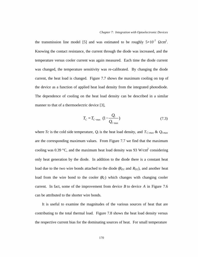
Chapter 7: Integration with Optoelectronic Devices
170
the transmission line model [5] and was estimated to be roughly 5×10⁻⁷ Ωcm2.
Knowing the contact resistance, the current through the diode was increased, and the
temperature versus cooler current was again measured. Each time the diode current
was changed, the temperature sensitivity was re-calibrated. By changing the diode
current, the heat load is changed. Figure 7.7 shows the maximum cooling on top of
the device as a function of applied heat load density from the integrated photodiode.
The dependence of cooling on the heat load density can be described in a similar
manner to that of a thermoelectric device [3],
where Tc is the cold side temperature, Ql is the heat load density, and TC-max & Ql-max
are the corresponding maximum values. From Figure 7.7 we find that the maximum
cooling was 0.39 °C, and the maximum heat load density was 93 W/cm2 considering
only heat generation by the diode. In addition to the diode there is a constant heat
load due to the two wire bonds attached to the diode (RD1 and RD2), and another heat
load from the wire bond to the cooler (RC) which changes with changing cooler
current. In fact, some of the improvement from device B to device A in Figure 7.6
can be attributed to the shorter wire bonds.
It is useful to examine the magnitudes of the various sources of heat that are
contributing to the total thermal load. Figure 7.8 shows the heat load density versus
the respective current bias for the dominating sources of heat. For small temperature
)1(max
max−
− −⋅=l
lCC Q
QTT (7.3)
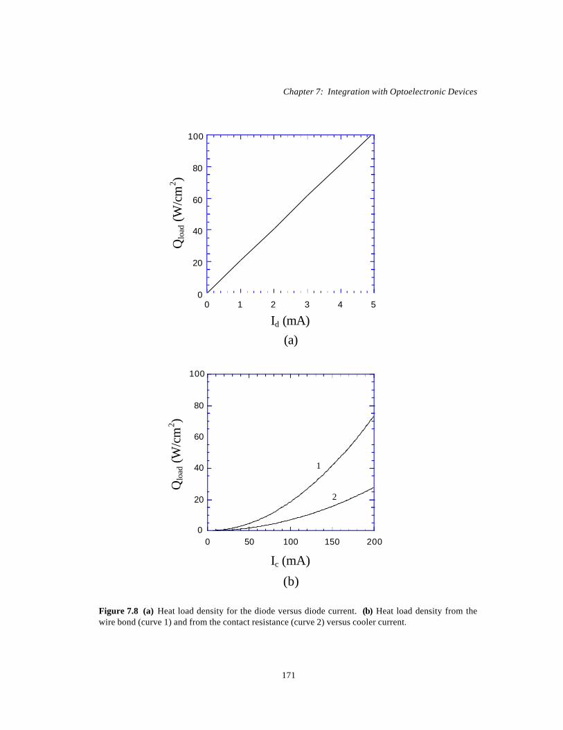
Chapter 7: Integration with Optoelectronic Devices
171
20
40
60
80
100
0 50 100 150 2000
Qlo
ad (W
/cm
2 )
Id (mA)
Figure 7.8 (a) Heat load density for the diode versus diode current. (b) Heat load density from thewire bond (curve 1) and from the contact resistance (curve 2) versus cooler current.
Qlo
ad (W
/cm
2 )
Ic (mA)
(a)
(b)
2
1
0
20
40
60
80
100
0 1 2 3 4 5

Chapter 7: Integration with Optoelectronic Devices
172
differences, it was assumed that approximately one half the heat generation in the
wire bonds arrives at the device while the other half goes to the heat sink. The heat
generation due to the diode contact resistance and wire bonds connected to the diode
is not shown since it was several orders of magnitude smaller because of the small
value of diode current. At the optimum cooler current bias of 160 mA (device B
from Figure 7.6), there is 47 W/cm2 of heat load density due to the wire bond
connected to the device and an additional 18 W/cm2 due to the contact resistance.
Using these values, the actual maximum heat load density was 158 W/cm2. This
result is more than a factor of ten better than the best bulk thermoelectric cooler.
7.3 1.55 µm InGaAsP Ridge Waveguide Laser
The next device investigated for monolithic integration of cooling was a 1.55-µm
InGaAsP ridge-waveguide laser. A schematic of the structure used is given in Figure
7.9. The growth was performed by MOCVD on a n-InP substrate. The thermionic
cooler structure was again the low barrier design (1-µm-thick superlattice, 25 periods
of 10/30nm InGaAs/InGaAsP, λ=1.3µm) surrounded by n+ InGaAs emitter and
collector layers that were 0.3µm and 0.5µm thick respectively. The laser structure
consisted of a 2-µm-thick n-InP cladding layer, an undoped InGaAsP active region
consisting of five quantum wells (λ=1.64µm) with a 0.3µm thick confinement layer
(λ=1.15µm) above and below, a 1.5µm thick p-InP cladding layer, and a 0.15µm
Chapter 7: Integration with Optoelectronic Devices
173
thick p-InGaAs contact layer. The ridge widths were varied from 20 to 50 µm, and
the metal contacts to the cooler were 50 µm wide and 10 µm from the edge of the
laser mesa. The lasers were cleaved to various lengths (100-300µm), mounted on
fabricated silicon packages, and wire bonded for testing. Two current sources were
used to independently control the current through the laser and cooler sections. An
SEM of the processed and packaged device is shown in Figure 7.10.
Figure 7.9 Schematic of thermionic cooler integrated with a ridge waveguide laser showing the laser(IL) and cooler (IC) bias.
p+ InGaAs
n+ InGaAs
n InP cladding
SCH & Active
p InP cladding
ID
IC
InP Substrate
InGaAs/InGaAsP SL

Chapter 7: Integration with Optoelectronic Devices
174
When designing the integrated structure, it was necessary to consider the
optical waveguiding properties of the cooler. The use of high refractive index
InGaAs material (n=3.587) in the superlattice barrier and contact layers results in an
excellent waveguide which must be isolated from the laser active region and separate
confinement heterostructure (SCH) region. A two-dimensional waveguide
simulation [6] was used to predict the necessary thickness of the lower n-InP
cladding region to eliminate mode leakage into the layers comprising the cooler.
Figure 7.11 shows a contour map of the normalized transverse-index profile and
corresponding simulation result of the modal confinement in the ridge waveguide.
Figure 7.10 SEM of a processed and packaged ridge laser and monolithically integrated cooler. Thelaser was mounted at the edge of a cleaved Si package to allow for coupling to a fiber probe. Thewire bond for the center stripe p-contact is not shown.
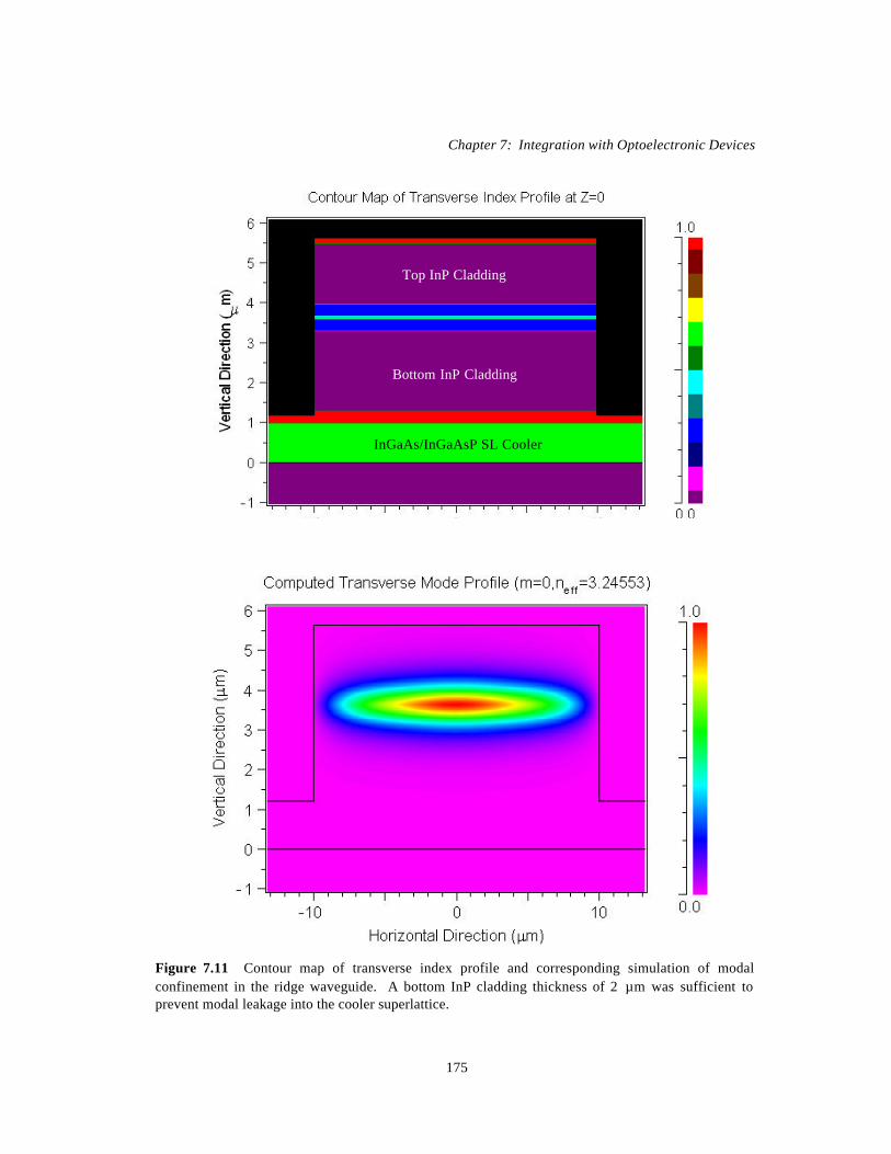
Chapter 7: Integration with Optoelectronic Devices
175
Figure 7.11 Contour map of transverse index profile and corresponding simulation of modalconfinement in the ridge waveguide. A bottom InP cladding thickness of 2 µm was sufficient toprevent modal leakage into the cooler superlattice.
Top InP Cladding
Bottom InP Cladding
InGaAs/InGaAsP SL Cooler
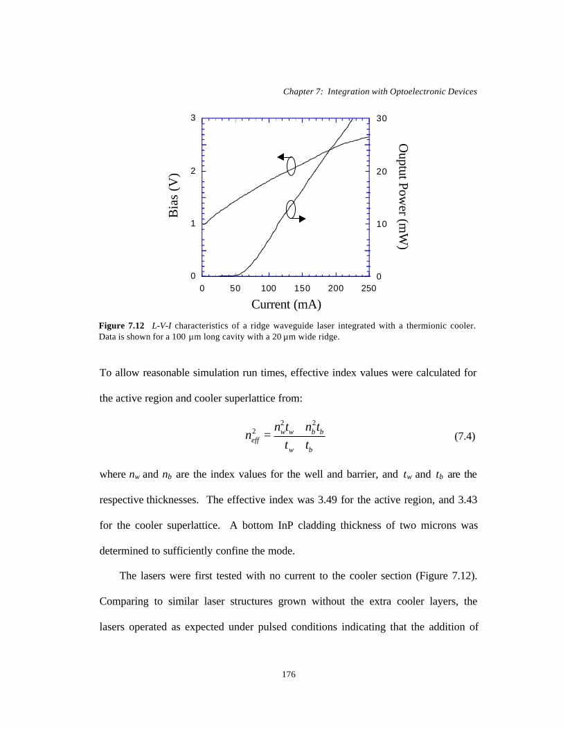
Chapter 7: Integration with Optoelectronic Devices
176
To allow reasonable simulation run times, effective index values were calculated for
the active region and cooler superlattice from:
where nw and nb are the index values for the well and barrier, and tw and tb are the
respective thicknesses. The effective index was 3.49 for the active region, and 3.43
for the cooler superlattice. A bottom InP cladding thickness of two microns was
determined to sufficiently confine the mode.
The lasers were first tested with no current to the cooler section (Figure 7.12).
Comparing to similar laser structures grown without the extra cooler layers, the
lasers operated as expected under pulsed conditions indicating that the addition of
0
1
2
3
0
10
20
30
0 50 100 150 200 250
Figure 7.12 L-V-I characteristics of a ridge waveguide laser integrated with a thermionic cooler.Data is shown for a 100 µm long cavity with a 20 µm wide ridge.
Current (mA)
Bia
s (V
)O
uptut Power (m
W)
bw
bbwweff tt
tntnn
++
=22
2 (7.4)

Chapter 7: Integration with Optoelectronic Devices
177
the thermionic cooler structure did not significantly impact the quality of the growth.
The emission wavelength was around 1.55 µm, and the temperature sensitivity was
measured to be approximately 0.1 nm/°C. This was then used to monitor the
temperature change of the laser versus cooler current. It was determined that the
laser would only heat for either current bias direction. To explain the observed
experimental results, a commercial laser diode simulator [7] was used to model the
integrated device. Simulation results indicated that the current injected from the
cooler contact was not spreading underneath the laser mesa negating any superlattice
barrier cooling effects (Figure 7.13). It was also determined that the InGaAs region
between the laser and cooler was not sufficiently thick enough to prevent a
substantial amount of laser current to penetrate into the cooler structure. This
reverse current through the cooler superlattice actually causes heating instead of
cooling. Figure 7.14 indicates the measured amounts of cooling at various points on
the device when there is no bias to the laser section. Only small amounts of cooling
are seen on the side contact, and hardly any cooling is measured on the laser mesa.
Surprisingly, the cooling results are in stark contrast to previously published
experiments with monolithically-integrated Peltier-cooled lasers [8-11]. In all of the
structures described, a metal contact was placed next to the laser and used to pass an
additional current through the substrate creating a simple thermoelectric cooler. In
these reports, cooling as large as 3 K was reported for InP substrates. Ignoring the
cooling properties of the superlattice in our structure, there should still remain a
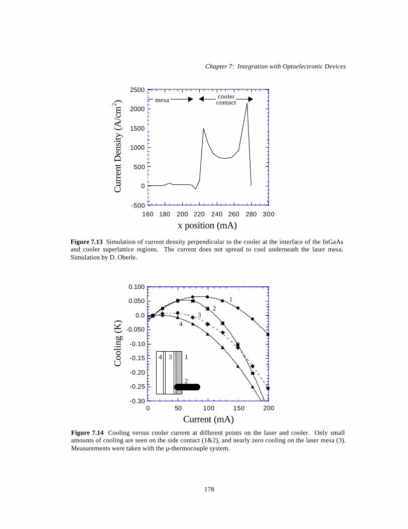
Chapter 7: Integration with Optoelectronic Devices
178
Figure 7.13 Simulation of current density perpendicular to the cooler at the interface of the InGaAsand cooler superlattice regions. The current does not spread to cool underneath the laser mesa.Simulation by D. Oberle.
x position (mA)
Cur
rent
Den
sity
(A/c
m2 )
-500
0
500
1000
1500
2000
2500
160 180 200 220 240 260 280 300
mesa coolercontact
-0.30
-0.25
-0.20
-0.15
-0.10
-0.050
0.0
0.050
0.100
0 50 100 150 200
1
Current (mA)
Coo
ling
(K)
Figure 7.14 Cooling versus cooler current at different points on the laser and cooler. Only smallamounts of cooling are seen on the side contact (1&2), and nearly zero cooling on the laser mesa (3).Measurements were taken with the µ-thermocouple system.
2
34
12
34
Chapter 7: Integration with Optoelectronic Devices
179
metal-semiconductor thermoelectric effect that would produce similar results. One
explanation is that our structures used more highly doped substrates and epi layers
resulting in a smaller Seebeck coefficient. This however, would at most result in a
factor of two reduction of cooling. The other possibility was discussed in detail in
Chapter 6 (Section 6.2.6). In this previous discussion of two-stage cooling, it was
shown that there exists an optimum ratio of currents, one through the side contact
and one through the substrate, that minimize heating effects. This minimization is
more crucial in lower doped structures where Joule heating in the substrate plays a
more involved role. Furthermore, even with no Peltier effects, the temperature
versus current through the side contact can still follow the second order polynomial
shape that is usually associated with cooling. Further investigation is needed to
clearly explain the discrepancies.
The packaging of the laser was also briefly examined. The IR Camera system
described in Chapter 6 (Section 6.1.4) was used to generate thermal images of a
packaged device under bias. Figure 7.15 shows an image for a laser current of 200
mA and zero cooler current. While quantitative data was not possible due to the
poor reproducibility of values, qualitatively more heating is observed on the topmost
side of the device. This temperature distribution is due to an increased thermal
resistance at the boundary of the Si package. More symmetric heat distributions
were seen when the device was mounted away from the edge of the package.
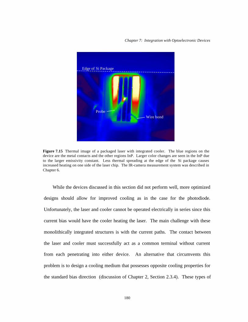
Chapter 7: Integration with Optoelectronic Devices
180
While the devices discussed in this section did not perform well, more optimized
designs should allow for improved cooling as in the case for the photodiode.
Unfortunately, the laser and cooler cannot be operated electrically in series since this
current bias would have the cooler heating the laser. The main challenge with these
monolithically integrated structures is with the current paths. The contact between
the laser and cooler must successfully act as a common terminal without current
from each penetrating into either device. An alternative that circumvents this
problem is to design a cooling medium that possesses opposite cooling properties for
the standard bias direction (discussion of Chapter 2, Section 2.3.4). These types of
Figure 7.15 Thermal image of a packaged laser with integrated cooler. The blue regions on thedevice are the metal contacts and the other regions InP. Larger color changes are seen in the InP dueto the larger emissivity constant. Less thermal spreading at the edge of the Si package causesincreased heating on one side of the laser chip. The IR-camera measurement system was described inChapter 6.
Edge of Si Package
ProbeWire bond

Chapter 7: Integration with Optoelectronic Devices
181
materials could exhibit p-type cooling properties with n-type doped structures, and
visa versa. Another possibility is to use heterogeneous integration which is
discussed further in the next section.
7.4 Long Wavelength VCSELs
In this section, the most recent ongoing work with integrated cooling for VCSEL
structures is presented. Many different approaches have been considered, but we
will mainly focus on heterogeneous integration to draw comparisons between the
monolithic integration work that was described in the last two sections.
Heterogeneous integration allows for more flexibility in material choice and better
optimization of the separate VCSEL and cooler structures, but still maintains some
constraints on design such as in the optical path.
We begin this section by discussing some of the relevant thermal issues in long
wavelength (1.55µm) VCSELs and VCSEL arrays. The arrays are primarily
intended for use in wavelength division multiplexed (WDM) short-reach optical
links since this wavelength corresponds to the loss minimum of optical fiber [12,13].
Following the discussion of VCSELs, SiGe-based thin-film micro-coolers are
examined. This material system currently provides the best available cooling, and
also lends itself well to the necessary processing and packaging steps. Finally, the
preliminary work on heterogeneous integration by Au-Au bonding is presented.
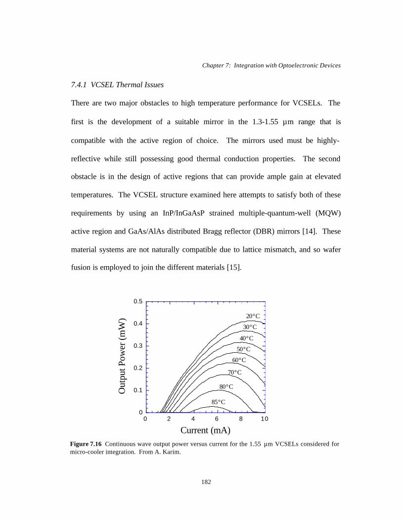
Chapter 7: Integration with Optoelectronic Devices
182
7.4.1 VCSEL Thermal Issues
There are two major obstacles to high temperature performance for VCSELs. The
first is the development of a suitable mirror in the 1.3-1.55 µm range that is
compatible with the active region of choice. The mirrors used must be highly-
reflective while still possessing good thermal conduction properties. The second
obstacle is in the design of active regions that can provide ample gain at elevated
temperatures. The VCSEL structure examined here attempts to satisfy both of these
requirements by using an InP/InGaAsP strained multiple-quantum-well (MQW)
active region and GaAs/AlAs distributed Bragg reflector (DBR) mirrors [14]. These
material systems are not naturally compatible due to lattice mismatch, and so wafer
fusion is employed to join the different materials [15].
0
0.1
0.2
0.3
0.4
0.5
0 2 4 6 8 10
Figure 7.16 Continuous wave output power versus current for the 1.55 µm VCSELs considered formicro-cooler integration. From A. Karim.
Current (mA)
Out
put P
ower
(mW
) 20°C
30°C
40°C
50°C
60°C
70°C
80°C
85°C

Chapter 7: Integration with Optoelectronic Devices
183
Figure 7.16 shows typical continuous-wave light versus current curves from
room temperature up to 85 °C. As the temperature is raised, threshold current
increases and differential efficiency decreases until the device no longer lases. The
overall reduction in output power over this temperature range is more than 12 dB.
Lasing ceases when the active region reaches a temperature for which it can no
longer provide the necessary gain to overcome cavity and mirror losses.
Unfavorably, the active region typically operates at a substantially higher
temperature than that of the heat sink, owing to the considerable thermal resistance
between the heat source and sink. Figure 7.17 plots the internal active region
temperature over current for a heat sink temperature of 20 °C. For moderate output
powers, the active region can be more than 30 °C above the heat sink temperature.
Figure 7.17 Active region temperature versus current plotted alongside output power for a heat sinktemperature of 20 °C. From A. Karim.
Current (mA)
Out
put P
ower
(mW
)
0
0.1
0.2
0.3
0.4
0.5
0
50
100
150
0 5 10 15 20
Active R
egion Temp (°C
)

Chapter 7: Integration with Optoelectronic Devices
184
Therefore, even with a thermoelectric cooler beneath the substrate, the device
temperature can be significantly higher. This can be even greater for structures that
include mirrors with a larger thermal resistance.
The heat generated by a single VCSEL can also impact the operation of other
devices in the array in the form of thermal crosstalk. To evaluate the crosstalk
theoretically, a 3-D ANSYS thermal simulation [16] was used to solve the surface
temperature surrounding a VCSEL. Figure 7.18 shows such a result for a 10 µm
pillar diameter sitting on a 7.7-µm-thick GaAs/AlAs DBR and 300-µm-thick GaAs
10 µm
250 µm
Figure 7.18 Thermal image of surface temperature from a 3-D ANSYS simulation of substrate heatflow for the long wavelength VCSEL structure. The pillar diameter was 10 µm, the bottom DBR was7.7 µm thick, and the GaAs substrate was 300 µm thick.

Chapter 7: Integration with Optoelectronic Devices
185
substrate. A worse case condition of a 100 °C operating temperature was assumed.
The temperature can be seen to drop off very quickly within 20 to 30 µm. An
approximate analytical formula for the temperature fall off can be expressed as:
where P is the power of the heat source, β lat is the effective lateral thermal-
conductivity, and r is the distance from the source [17,18]. Figure 7.19 compares the
simulation result to experimentally measured surface temperatures. While the
experimental values fit well to Equation 7.5, the simulation values dropped off more
steeply showing a stronger inverse dependence on area. This can be explained by the
rP
rTlatπβ2
)( = (7.5)
0
10
20
30
40
50
0 50 100 150 200 250 300
Figure 7.19 Comparison of simulated and measured surface temperature versus distance from theVCSEL heat source. The two curves show differing area dependence.
Distance (µm)
Surf
ace
Tem
pera
ture
(°C
)
Simulation ∝ r-1.77
Measurement ∝ r-1

Chapter 7: Integration with Optoelectronic Devices
186
presence of a boundary thermal resistance at the bottom of the heat sink which was
not included in the simulation. Evidently, the thermal floor in Figure 7.19 depends
on the mounting of the sample to the heat sink. In any case, the experimental values
show about 5% of the VCSEL’s peak temperature is present 300 µm away from the
sample. If another device in the array was also operating, the elevated temperature
would affect the output power and emission wavelength. As an example, if a single
VCSEL in an array with 300-µm-pitch employing a wavelength spacing of 0.2 nm
requires a temperature stabilization of ± 0.5 °C, the nearest operating device could
not heat up beyond 5 °C unless some other active tuning mechanism is used.
Thermal crosstalk may be even more of an issue for structures that employ lateral
heat spreading layers such as in all-epitaxial long wavelength VCSELs [19].
Reduction in crosstalk is possible by short-circuiting the lateral heat spreading by
flip-chip bonding to a good heat sink, but there would still be no control over
emission wavelength. Flip chipping to Si-based micro-coolers would allow for
integration with both cooling elements and drive electronics.
7.4.2 SiGe Micro-Coolers
Since heterogeneous integration allows for the use of dissimilar materials, the best
available thin-film micro-cooler should be used. Recent work on Si1-xGex/Si [20]
and SiGeC/Si [21] superlattice structures have shown impressive cooling
performance. Fan et. al. have demonstrated maximum cooling values of 4 to 12 K

Chapter 7: Integration with Optoelectronic Devices
187
0
2
4
6
8
10
12
14
0 100 200 300 400 500 600
current, mA
25 oC
100 oC
150 oC
200 oC
Figure 7.20 Cooling versus current and heat sink temperature for a 3-µm-thick, 50×50 µm2, 12/3nmSiGe/Si superlattice cooler [20]. From X. Fan and G. Zeng.
Current (mA)
Coo
ling
(K)
-1
-0.5
0
0.5
1
1.5
2
2.5
3
0 200 400 600 800 1000
Figure 7.21 Measured maximum cooling versus heat load for a 2-µm-thick 40×40 µm2 SiGeC thinfilm cooler [21]. The heat sink temperature was 70 °C. From X. Fan and G. Zeng
Heat Load (W/cm2)
Coo
ling
(K)

Chapter 7: Integration with Optoelectronic Devices
188
with SiGe/Si superlattices (Figure 7.20), and cooling power densities exceeding 900
W/cm2 for SiGeC/Si superlattices (Figure 7.21). These devices are currently being
investigated for integration with Si-based microelectronics, and work is underway to
further improve performance with thermionic emission in heterostructures [22].
7.4.3 Heterogeneous Integration
Two procedures have been investigated for heterogeneous integration of coolers with
optoelectronic devices. In the first process, blanket evaporation of Ti/Pt/Au
(200/1000/5000Å) onto both the unprocessed cooler and optoelectronic wafer is first
performed. Then, under the Au-Au bonding conditions outlined in Chapter 5, the
two samples are fused together. Finally, a series of etches and metallization steps are
completed to define the device and cooler stages. Successful attempts at bonding
VCSELs in this manner have been reported [23], but a 1.5-µm-thick layer of In was
used as well. This is best avoided to keep the thermal conductivity as high as
possible at the bonded interface. Previous reports on pure Au-Au bonding have been
successful for in-plane micro-strip lasers [24]. Our results for this procedure, which
were discussed in Chapter 5 (Section 5.4), showed roughly a 50% yield with test
structures. If this method is used for cooler integration with VCSELs, the design
must be top emitting due to the underlying metal layers.
In the second procedure considered, the VCSELs and cooler wafers are first
separately processed, and then flip-chip bonded to each other. It is still desirable to
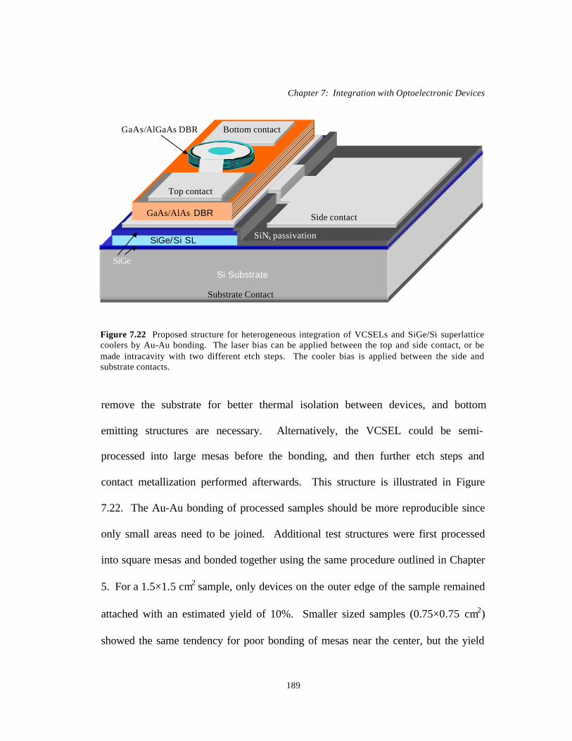
Chapter 7: Integration with Optoelectronic Devices
189
remove the substrate for better thermal isolation between devices, and bottom
emitting structures are necessary. Alternatively, the VCSEL could be semi-
processed into large mesas before the bonding, and then further etch steps and
contact metallization performed afterwards. This structure is illustrated in Figure
7.22. The Au-Au bonding of processed samples should be more reproducible since
only small areas need to be joined. Additional test structures were first processed
into square mesas and bonded together using the same procedure outlined in Chapter
5. For a 1.5×1.5 cm2 sample, only devices on the outer edge of the sample remained
attached with an estimated yield of 10%. Smaller sized samples (0.75×0.75 cm2)
showed the same tendency for poor bonding of mesas near the center, but the yield
Figure 7.22 Proposed structure for heterogeneous integration of VCSELs and SiGe/Si superlatticecoolers by Au-Au bonding. The laser bias can be applied between the top and side contact, or bemade intracavity with two different etch steps. The cooler bias is applied between the side andsubstrate contacts.
Si Substrate
SiGe/Si SL
Side contactGaAs/AlAs DBR
GaAs/AlGaAs DBR
Substrate Contact
SiGe
Top contact
SiNx passivation
Bottom contact

Chapter 7: Integration with Optoelectronic Devices
190
increased to roughly 50%. An SEM of a bonded sample is shown in Figure 7.23.
While the quality of the bond is difficult to see visually, the mesas that did remain
attached survived violent agitation with solvents. Further electrical and thermal
evaluation of the test structures or of integrated devices should indicate the quality
and uniformity of the Au-Au bond. While it may be justified to include thin layers
of In or Sn to accommodate imperfections in the smooth metal surface, the trade-offs
between thermal resistance, bond uniformity, and yield should be optimized. A
thorough investigation of Au-Sn eutectic thermal conductivity would also be useful.
In either of the two procedures considered, the problems of isolation between
the device and cooler current are solved. The metal between the integrated devices
Figure 7.23 SEM of a Au-Au bonded test structure. While the quality of the bond is difficult to seevisually, the mesas remained attached after violent agitation with solvents.
InP epi
InGaAs stop etch
Au
Au
Bonded interface
Chapter 7: Integration with Optoelectronic Devices
191
serves as an ideal electrical common, and even intracavity contacts could be used in
some of the integrated geometries described.
7.5 Summary
There are many issues to consider for integration of cooling with optoelectronic
devices. While conventional thermoelectric coolers currently provide larger
temperature differences, they can only control the temperature of the substrate and
are limited in their cooling power density. Thin-film thermionic and thermoelectric
coolers can be integrated with optoelectronic devices to provide active temperature
stabilization, wavelength tuning, and large cooling power densities far beyond bulk
Peltier coolers. Several integration examples have been described, and the issues
with monolithic versus heterogeneous integration have been discussed. Precise
spatial control of temperature as well as fast transient times have been demonstrated.
With further improvement in cooling performance and integration methods,
thermionic cooling can be a viable supplement, and even replacement for
conventional thermoelectric coolers.
REFERENCES
1. S.M. Sze, Physics of Semiconductor Devices. New York: Wiley, 1981.
2. A. Fitting, J. Christofferson, A. Shakouri, X. Fan, G. Zeng, C. LaBounty, J.E. Bowers, E. CrokeIII, “Transient response of thin film SiGe micro coolers,” to be submitted.
3. D.M. Rowe, CRC Handbook of Thermoelectrics, CRC, New York, 1995.

Chapter 7: Integration with Optoelectronic Devices
192
4. J.M. Swartz, J.R. Gaines, “Wide range thermometry using gallium arsenide sensors,”Measurement & Control in Science & Industry, Vol. 4, 1972.
5. G.K. Reeves, H.B. Harrison, “Obtaining the specific contact resistance from transmission linemodel measurements ,” Elec. Dev. Lett., Vol. EDL-3, No.5, 1982, p. 111-3.
6. BeamPROP 3.0d by Rsoft™, 1999.
7. PICS3D 4.1.2 by Crosslight Software, 1998.
8. N.K. Dutta, W.S. Hobson, J. Lopata, G. Zydzik, “Tunable InGaAs/GaAs/InGaP laser,” Appl.Phys. Lett., Vol. 70, No.10, 1997, p. 1219-20.
9. P.R. Berger, N.K. Dutta, K.D. Choquette, G. Hasnain, N. Chand, “Monolithically Peltier-cooledvertical-cavity surface-emitting lasers,” Appl. Phys. Lett., Vol 59, No.1, 1 July 1991, pp. 117-9.
10. N.K. Dutta, T. Cella, R.L. Brown, D.T.C. Huo, “Monolithically integrated thermoelectriccontrolled laser diode,” Appl. Phys. Lett., Vol. 47, No. 3, (1 August 1985), pp. 222-4.
11. S. Hava, R.G. Hunsperger, H.B. Sequeira, “Monolithically Peltier-Cooled Laser Diodes,” Journalof Lightwave Technology, Vol.LT-2, No.2, 1984, p. 175-80.
12. A. Karim, P. Abraham, D. Lofgreen, Y.J. Chiu, J. Piprek, J.E. Bowers, “Wafer-bonded 1.55 µmvertical cavity laser arrays for wavelength division multiplexing,” Elec. Lett., Vol. 37, No.7,2001, p. 431-2.
13. V. Jayaraman, M. Kilcoyne, “WDM array using long-wavelength vertical cavity lasers ,” Proc.SPIE, Vol. 2690, 1996, p. 325-6.
14. A. Karim, K.A. Black, P. Abraham, D. Lofgreen, Y.J. Chiu, J. Piprek, and J.E. Bowers,“Superlattice Barrier 1528-nm Vertical-Cavity Laser with 85 °C Continuous-Wave Operation,”IEEE Photon. Tech. Lett., Vol. 12, No.11, 2000, p.1438-40.
15. A. Black, A.R. Hawkins, N.M. Margalit, D.I. Babic, A.L. Holmes Jr., Y.L. Chang, P. Abraham,J.E. Bowers, E.L. Hu, “Wafer fusion: Materials issues and device results ,” IEEE J. Select. TopicsQuantum Electron., Vol. 3, 1997, p. 943-51.
16. ANSYS Release 5.5.3 (1999) by Swanson Analysis Systems, Inc., Houston, PA.
17. T. Wipiejewski, D.B. Young, B.J. Thibeault, L.A. Coldren, “Thermal Crosstalk in 4×4 Vertical-Cavity Surface-Emitting Laser Arrays,” IEEE Photon. Tech. Lett., Vol. 8, No.8, 1996, p.980-2.
18. W. Nakwaski, M. Osinski, “Thermal resistance of top-surface-emitting vertical-cavitysemiconductor lasers and monolithic two-dimensional arrays,” Electron. Lett., Vol. 28, 1992,p.572-4.
Chapter 7: Integration with Optoelectronic Devices
193
19. E. Hall, G. Almuneau, J.K. Kim, O. Sjolund, H. Kroemer, L.A. Coldren, “Electrically-pumped,single-epitaxial VCSELs at 1.55 µm with Sb-based mirrors,” Electon. Lett., Vol.35, 1999,p.1337-8.
20. X. Fan, G. Zeng, C. LaBounty, E.Croke, D. Vashaee, A. Shakouri, C. Ahn, J.E. Bowers, “Highcooling power density SiGe/Si micro coolers,” Elec. Lett., Vol. 37, No.2, 2001, p. 126-7.
21. X. Fan, G. Zeng, C. LaBounty, E.Croke, A. Shakouri, C. Ahn, J.E. Bowers, “SiGeC/Sisuperlattice micro cooler,” Applied Physics Lett., Vol. 78, No.11, 2001, p. 1580-2.
22. X. Fan, G. Zeng, C. LaBounty, D. Vashaee, J. Christofferson, A. Shakouri, J.E. Bowers,“Integrated Cooling for Si-based Microelectronics ,” 20th International Conference onThermoelectrics, Beijing, China, June 2001, to be published.
23. H.J.J. Yeh, J.S. Smith, “Integration of GaAs Vertical-Cavity Surface Emitting Laser on Si bySubstrate Removal,” Applied Physics Lett., Vol. 64, March 1994, p. 1466-8.
24. D. Tauber, M. Horita, J. Piprek, P. Abraham, A.L. Holmes, J.E. Bowers, “The microstrip laser,”Photonics Technology Letters, Vol. 10, 1998, p. 478-80.

Chapter 7: Integration with Optoelectronic Devices
194

Chapter 8: Conclusions and Future Work
195
Chapter 8
Conclusions and Future Work
This thesis presents the first comprehensive examination of a novel type of micro-
cooler for integrated cooling applications with optoelectronic devices. Through the
use of thermionic emission in semiconductor heterobarriers, enhancements in the
material cooling properties can greatly exceed that of the constituent bulk material
values. Throughout the preceding chapters, the theory, design, processing,
characterization, and analysis of single-stage and integrated structures has been
discussed in detail. The first experimental demonstration of cooling was completed,
as well as the first demonstration of integrated cooling. While a great deal of
progress was made in the development of these devices, we are still far from
realizing their full potential. Continued work in this area is expected to meet much
success.
8.1 Summary
Throughout the first five chapters, the evolution of thermionic cooler development
was described step-by-step from basic theory through to the processing and
packaging. The introduction of Chapter 1 outlined the current technologies for solid-
state cooling of optoelectronics and provided the motivation for this research. The
fundamental goal of improving the cooling figure-of-merit ZT was also defined, as

Chapter 8: Conclusions and Future Work
196
well as the advantages of integrated cooling versus passive thermal management or
conventional thermoelectric coolers. Chapter 2 explained the physics behind
thermionic emission cooling, and theoretical calculations were developed to predict
an order of magnitude improvement in ZT for InP-based heterostructures. From
these theoretical models and calculations, design guidelines were assembled and
applied to the material structures described in Chapter 3. Several different InP-based
heterobarrier designs were investigated, each with a different barrier height.
Material characterization was described in Chapter 4, where the focus was on the
parameters that make up ZT. The material values measured were also essential in
creating the device simulations used in later chapters. The processing procedure was
given in Chapter 5, followed by the packaging evolution. The optimization of
packaging was a crucial step in analyzing cooler performance since poor packaging
can dominate the device non-ideal effects, and mask any differentiation from sample
to sample. Chapter 6 provided a thorough look at single-stage cooling performance
and analysis. The enabling contributors to this section were the development of new
micro-scale thermal measurement systems and accurate device simulation programs.
Also in this chapter, another new type of cooler structure was presented, the two-
stage three-terminal TITE cooler. The work described in the first six chapters was
then finally brought together and applied toward integrated cooling structures with
several different optoelectronic devices.

Chapter 8: Conclusions and Future Work
197
8.2 Future Work
Since this is such a novel device, the possibilities for future work are endless. Even
the general concept of micro-cooling is in its infancy, and an infinite number of
research projects exist in this field. From just a materials perspective, the shear
number of material combinations that could implement the concepts described in this
work are impressive. Likewise, countless optoelectronic and microelectronic devices
could benefit from integrated cooling. Keeping this in mind, this section considers
only a few of the most logical and attractive directions for future work.
8.2.1 Further Cooler Development and Integration
As stated above, the thermionic coolers are still far from being fully optimized in the
InP-based material system, and continued work is necessary to approach the
performance predicted by the simulations of Chapter 6. The non-ideal effects of
contact resistance, side contact Joule heating and heat conduction, and substrate
thermal resistance are all still limiting the maximum achievable cooling. The Joule
heating and heat conduction from the side contact have already been minimized for
single-stage coolers, however, by integrating p- and n-type coolers together, this
effect can be completely eliminated (see Section 8.2.2). Ways to reduce the
substrate thermal resistance have already been described in Chapter 5, but a reliable
process for substrate transfer still needs to be developed. Once the non-ideal effects
Chapter 8: Conclusions and Future Work
198
are further minimized, evaluation of different heterobarrier designs will be clearer,
and optimization easier.
The shortcomings of the integrated structures were clearly defined in Chapter 7.
From this work, better designs for monolithic integration should be considered,
keeping in mind the need to control the electrical current and thermal heat flow.
Probably the quickest path to success would be from further work on heterogeneous
integration since it is more straightforward to optimize each device separately, and
the careful control of current paths is not an issue.
8.2.2 Multi-element Coolers
The integration of n- and p-type thermionic coolers allows for the removal of
parasitic external electrical contacts, and can provide larger cooling capacities with
smaller currents. This could be done on a small scale with just a few elements, or on
a larger scale with the maximum cooling area limited only by the growth wafer
diameter. It was already shown in Chapter 6 that n and p devices could operate
under similar conditions, and the work on substrate transfer and heterogeneous
integration should provide the basis for making multi-element coolers. Large sized
modules would be expected to compete with conventional thermoelectric coolers,
while small area devices would retain their niche as micro-coolers for small-scale
integrated cooling (Figure 8.1).

Chapter 8: Conclusions and Future Work
199
8.2.3 Heat-to-Light Energy Conversion
The greatest detriment to the cooling efficiency of heterostructure thermionic
emission coolers is the heat conduction across the thin material between the cold and
hot side of the device. What if, however, the hot carriers arriving to the anode
junction were to loose their excess energy in the form of light instead of heat?
Figure 8.2 shows such a structure with an intersubband light-emitting thermionic
cooler [1,2]. The idea of a refrigerator without a hot side at first appears to violate
the 2nd law of thermodynamics by reducing the total entropy. However, by emitting
incoherent light, the increased disorder of the photons can maintain entropy
conservation.
Figure 8.1 Example of n- and p-type cooler integration for small scale cooling of individual VCSELs
VCSEL
p-type coolers n-type coolers

Chapter 8: Conclusions and Future Work
200
8.2.4 Miniband Superlattice Coolers
This concept of n-type devices behaving as p-type for thermoelectric purposes was
discussed at the end of Chapter 2. Theoretical calculations of an n-type superlattice
showed that if the Fermi level was placed at an optimum level above a miniband, and
the barrier above the Fermi level effectively blocked transmission of hot electrons,
then the n-type material could exhibit p-type cooling properties. This would make it
possible to make n- and p-type cooling elements with an all majority carrier
structure. It would also allow for the integration of a laser and cooler that was
electrically in series, avoiding the problems encountered with the monolithic
integration design. The laser would effectively be self-cooled, as any increase in
laser current would also increase the cooling at the same time. The main challenge
in designing such structures is maintaining a sufficient electrical conductivity to keep
Figure 8.2 An intersubband light-emitting thermionic cooler. Light emission must be incoherent tonot violate the 2nd law of thermodynamics. From A. Shakouri

Chapter 8: Conclusions and Future Work
201
ZT as high as possible. For this, the miniband should be as wide in energy as
possible while still providing a barrier to electrons above the Fermi level.
8.2.5 Vacuum Thermionics
In Section 8.2.3, heat-to-light energy conversion was suggested as a means to reduce
the amount of heat coming from the hot side of the device, thus increasing the
efficiency. The ultimate solution to eliminating this back flow of heat is to remove
the conducting medium completely, leaving only vacuum. Vacuum thermionics
were mentioned in Chapter 2, but because of the large work functions involved, only
high temperature applications exist. However, with current high-precision epitaxial
growth techniques and semiconductor processing technology, close and uniform
spacing of the cathode and anode can be achieved with atomic resolutions. By
growing a three layer structure with materials that have a known selective etch, the
center layer can be removed leaving an air gap between the two remaining materials.
Some form of mechanical support with good electrical and thermal insulation would
of course be needed. The close spacing of the electrodes should allow for efficient
cooling at room temperature with efficiencies approaching the ideal Carnot value.
8.3 Final Comments
Research on thermionic emission cooling in heterostructures has made great progress
in a short period of time. This quick progress has supported the drive to apply these
Chapter 8: Conclusions and Future Work
202
devices in integrated structures for optoelectronic devices. Already, significant
improvements beyond the cooling capabilities of bulk InP-based materials have been
demonstrated. While these unique coolers serve a certain niche of high cooling-
power-density microscale cooling, much more work is necessary before they can
compete with traditional thermoelectric coolers in terms of attainable temperature
differentials. Finally, while the concepts developed throughout this work were for
InP-based materials, they are also universally applicable to any material system for
which band structure engineering is possible.
REFERENCES
1. A. Shakouri, J.E. Bowers, “Heterostructure integrated thermionic refrigeration,” Proceedings of16th International Conference on Thermoelectrics, Dresden, Germany, August 1997, p. 636-40.
2. J. Faist, F. Capasso, D.L. Sivco, C. Sirtori, A.L. Hutchinson, A.Y. Cho, “Quantum cascade laser,”Science, Vol. 264, 1994, p.553.

Appendix A
203
Appendix A
General Thermoelectric Device Theory
While a detailed discussion of thermoelectric theory is beyond the scope of this
thesis, the purpose of this section is to familiarize the reader with some of the basic
concepts that will apply in many cases to thermionic emission cooling as well. A
more detailed source of thermoelectric theory can be found elsewhere [1,2].
To discuss the basic concepts in thermoelectric theory, consider two junctions
between two dissimilar thermo-elements as shown in Figure A.1a. At given
temperatures T1 and T2, a voltage is generated. The change in voltage, ∆V, is
proportional to the change in temperature, ∆T=T1 – T2, by the Seebeck coefficient S.
This electrical potential is generated as a result of the temperature gradient in the
material.
If we now pass a current I through the same elements as in Figure A.1b, a heat
current of +Q will be generated at one interface, and a heat current of –Q will be
absorbed at the other. This relationship between heat and electrical current is the
Peltier coefficient, π , which results from the change in entropy of the electrical
charge carriers as they cross a junction.
The last effect to present is the Thompson effect which is illustrated in Figure
A.1c. In any non-isothermal homogeneous conductor with an electrical current,
heat is either absorbed or generated and can be described by the Thompson

Appendix A
204
coefficient γ = ∆Q/I⋅∆T. This phenomenon is a consequence of the direction of
electrical carriers with respect to a temperature gradient within a conductor.
Finally it is important to note the relationship between the Seebeck and Peltier
coefficients, π = S ⋅ T. This relation plays an important role in thermoelectrics and
will be used below in the expression for cooling capacity.
TV
S∆∆
=Seebeck: ab
∆V
T1
a
T2
(a)
I
Q Q
IQ
baab =−= πππPeltier: ab
a(b)
bT1 T2
Q
I
TIQ∆⋅
∆=γThomson:(c)
Figure A.1 Physical description of thermoelectric phenomenon of interest, (a) Seebeck effect, (b)Peltier effect, and (c) Thomson effect.

Appendix A
205
Starting from the structure presented above for n- and p-type elements, and
optimizing the geometry for cooling, we arrive at the conventional thermoelectric
configuration shown in Figure A.2. In this arrangement, both n- and p-type elements
are placed electrically in series and thermally in parallel. When a current is passed
through the structure, a net cooling occurs on the top of the elements and a net
heating at the bottom. This is due to the fact that the Peltier effect is reversed for n-
and p-type elements with the same direction of current flow.
The operation of the device can be described quantitatively by the expression for
cooling capacity,
where S is the Seebeck coefficient, TC is the cold side of the cooler, I is the electrical
current, R is the electrical resistance, β is the thermal conductivity, and ∆T is the
TRIISTQ C ∆−−= β2
21
(A.1)
Cold (T1)
II
Q
Hot (T2)
p n
Figure A.2 Single element of a cooler in a conventional thermoelectric configuration, with n- and p-type thermoelements electrically in series and thermally in parallel.

Appendix A
206
temperature difference between the hot and cold side junctions. The first term
describes the Peltier cooling, the second term describes the amount of Joule heat in
the legs that arrives back to the cold junction, and the third term relates to the heat
conduction between the hot and cold junctions.
The coefficient of performance (COP) of a TE cooler is the ratio of cooling
capacity to the amount of input power, and can be expressed as,
For given material parameters, geometries, and hot and cold junction temperatures,
Q and COP have their optimum values at different currents. The current, Imax cool,
gives the maximum cooling, and Imax COP the maximum coefficient of performance:
In practical TE cooling applications, the current is typically chosen in the range
between the maximum efficiency and the maximum cooling power. From Equation
RIITS
TRIIST
WQ
COPC
2
2
21
+⋅∆⋅
∆−−==
β(A.2)
RST
I Ccool =max
)11(
)(max
−+
−=
ZTR
TTSI
C
HCCOP
22/12/1
2
+
=
n
n
p
p
SZ
σβ
σ
β
(A.3)
(A.4)
(A.5)
Appendix A
207
A.1 it can be seen that a positive cooling effect (Q ≥ 0) can not be achieved if the
temperature difference between the junctions is too great. The maximum
temperature difference is found by setting Q = 0, and substituting Equation A.3:
From this result, the relevance of the Z parameter is obvious as it describes both the
maximum temperature difference achievable and the COPmax. Expressing Z of a
single branch as S2σ/β , it specifies how “good” the material is for thermoelectric
cooling applications and is therefore called the thermoelectric figure-of-merit.
While in this discussion we have concentrated on the cooling applications of
thermoelectrics, it is also possible to operate these devices in reverse and generate
power from a given temperature gradient. The optimization is slightly different as it
is the power factor, S2σ that needs to be optimized.
REFERENCES
1. H.J. Goldsmid, Electronic Refrigeration, Pion Limited, 1986.
2. D.M. Rowe, CRC Handbook of Thermoelectrics, CRC, New York, 1995.
2max 2
1coldZTT =∆ (A.6)