gate line edge roughness model for estimation of finfet...
TRANSCRIPT

IEEE TRANSACTIONS ON ELECTRON DEVICES, VOL. 56, NO. 12, DECEMBER 2009 3055
Gate Line Edge Roughness Model for Estimationof FinFET Performance Variability
Kedar Patel, Senior Member, IEEE, Tsu-Jae King Liu, Fellow, IEEE, and Costas J. Spanos, Fellow, IEEE
Abstract—We present a model for estimating the impact ofgate line edge roughness (LER) on the performance of double-gate (DG) FinFET devices. Thirteen-nanometer-gate-length DGFinFETs are investigated using a framework that links deviceperformance to commonly used LER descriptors, namely, corre-lation length (ξ), rms amplitude or standard deviation (σ) of theline edge from its mean value, and roughness exponent (α). Ourapproach provides physical insight into how LER impacts FinFETperformance. In addition, our modeling approach is more efficientthan Monte Carlo TCAD simulations and provides comparableresults with appropriately selected input parameters. The FinFETdevice architecture is found to be robust to gate LER effects. Fur-thermore, a spacer-defined gate electrode (versus a resist-definedgate electrode) provides for reduced variability in performance,indicating that the gate length mismatch has more impact thanlateral offset between the front and the back gates.
Index Terms—Double gate (DG), FinFET, intrinsic parameterfluctuation, line edge roughness (LER), variability.
I. INTRODUCTION
INTRINSIC process parameter fluctuations cause undesir-able performance mismatch in identically designed transis-
tors. As the dimensions of the transistors are scaled down, thismismatch increases and, hence, has greater impact on the circuitperformance and yield. The primary sources of transistor per-formance variability that have emerged are line edge roughness(LER), gate dielectric thickness (tox) variation, random dopantfluctuations (RDFs), and metal-gate work function (WFV) [1],[2]. Advanced transistor structures such as the double-gate(DG) FinFET [3] are more robust to tox variation and RDFbecause a thin body is used to suppress short-channel effects(SCEs), without the need for channel/body doping. In a recentstudy, FinFETs have been found to have lower threshold voltagevariability due to LER [4]. Due to the challenges with scalingplanar bulk MOSFETs, advanced structures such as FinFETmay be adopted as early as the 25-nm CMOS technologynode [5].
Manuscript received March 24, 2009; revised August 14, 2009. First pub-lished October 30, 2009; current version published November 20, 2009. Thiswork was supported in part by FLCC/IMPACT, an industry and academiaalliance with support from the UC Discovery Grant Program. The review ofthis paper was arranged by Editor D. Esseni.
K. Patel is with SanDisk Corporation, Milpitas, CA 95035 USA, and alsowith the University of California, Berkeley, CA 94720 USA (e-mail: [email protected]).
T.-J. K. Liu and C. J. Spanos are with the Department of ElectricalEngineering and Computer Sciences, University of California, Berkeley,CA 94720 USA.
Color versions of one or more of the figures in this paper are available onlineat http://ieeexplore.ieee.org.
Digital Object Identifier 10.1109/TED.2009.2032605
LER is stochastic and is affected by many factors duringpattern definition. It is a fundamental consequence of resistprocessing: Erosion of polymer aggregates at the edges of aresist during development has been shown to create a roughprofile [6], [7]. In this paper, we examine the impact of LER onFinFET performance. Earlier work on understanding the effectsof LER on device performance was either focused on planarbulk CMOS [8] or followed a computationally expensive MonteCarlo (MC) approach [9]. Due to the stochastic nature of LER,an accurate estimate of device performance variability can onlybe achieved through a full MC 3-D device simulation. However,this computational approach is prohibitively expensive and doesnot provide insight into how LER impacts device performance.Our premise is that LER manifests itself in the form of offsetbetween the front gate (FG) and the back gate (BG), as well asthe difference in FG and BG critical dimensions. As such, webelieve that the 2-D transistor structure is sufficient to capturethe effects due mismatched FG and BG. Therefore, in thispaper, we develop a computationally efficient statistical modelthat is formulated to link the characteristic LER descriptors todevice performance variability. The organization of this paper isas follows: In Section II, we provide a brief background on LERand its characteristic descriptors. In Section III, we describethe details of the 2-D device simulation and the formulation ofour model. The simulated device structure is designed to meetthe ITRS specifications for the 32-nm high-performance (HP)CMOS technology node. Finally, in Section IV, we discuss theresults of our work. The impact of gate length variation andlateral offset between the FG and BG is studied. Sensitivityof key performance parameters such as saturation thresholdvoltage (Vt,sat), ON-state saturation drive current (Id,sat), andOFF-state leakage current (Ioff) to the various LER parametersis discussed.
II. LER
A. Background
LER and linewidth roughness (LWR) are often used syn-onymously. Mathematically, they are related but different. Asshown in Fig. 1, LER refers to the fluctuations of a givenline edge about its mean value, whereas LWR corresponds tofluctuations in a linewidth about its own mean value. For a linesampled at N points along the width W , LWR is described bythe variance in the linewidth as
σ2LWR = (N − 1)−1
N∑i=1
(Li − L)2. (1)
0018-9383/$26.00 © 2009 IEEE

3056 IEEE TRANSACTIONS ON ELECTRON DEVICES, VOL. 56, NO. 12, DECEMBER 2009
Fig. 1. LER is the fluctuation of a line about its mean value for a given edge.LWR is the fluctuation of a linewidth Li about its mean value 〈L〉 averagedover the width W .
LWR can also be described in terms of variability of eachindividual edge as
σ2LWR = σ2
L + σ2R − 2ρXσLσR (2)
where the subscripts “L” and “R” refer to the left and rightedges of a line, respectively, and ρX is the cross-correlationcoefficient between them. The value of ρX depends primarilyon the method of line formation, as will be described later inthis paper. If we assume that
σL = σR ≡ σLER (3)
then we can simplify (2) to
σ2LWR = 2σ2
LER(1 − ρX). (4)
The variance or, alternately, the sigma value does not providea complete description of LER [10], [11]. The shortfall of thesigma value arises primarily due to the spatial spectral contentof roughness along the edge. In order to capture that spec-tral content, we invoke the formulation of the autocorrelationfunction, which describes the correlation between points of astationary random process such as the one that is responsiblefor LWR formation. For a stationary LWR profile, the autocor-relation between two points is only a function of distance (or“lag”) between them. Similarly, for a jointly stationary LWRprofile, the cross-correlation coefficient described in (4) is alsoonly a function of the lag between them. In describing LWR,it is convenient to approximate the autocorrelation coefficientwith a closed-form expression given by [12]
ρA(y) = exp[−(y/ξ)2α
](5)
where y is the lag, ξ is the correlation length, and α is theroughness exponent. The correlation length denotes the dis-tance beyond which the amplitudes of two points along an edgecan be considered almost uncorrelated. The roughness exponentis a relative measure of the high-frequency component in theroughness; larger values correspond to fewer high-frequencyamplitude variations. The simulated effect of each parameteron roughness is shown in Fig. 2. The algorithm used to generatethe LWR profiles in this paper is briefly as follows: The powerspectrum in (5) and the Gaussian noise are convolved in the
frequency domain to obtain the Fourier transform of the outputedge; the output edge in the spatial domain is obtained by per-forming a subsequent inverse Fourier transform. In generatingan LWR profile, proper care must be taken to avoid samplingnear the edge of the profile due to artifacts of discrete FFT on afinite series.
It should be pointed out that (5) represents just one formof a plausible autocorrelation function. Other forms such asexponentially decaying sinusoid can also be used [13]. Inthis paper, we follow the convention introduced in [12], andwe, therefore, assume that LWR can completely be describedby three parameters: correlation length (ξ), rms amplitude orstandard deviation (σ) of the line edge from its mean value,and roughness exponent (α) [10], [11].
B. Spacer Versus Resist Lithography
In a FinFET fabrication process, the gate electrode can bedefined in one of two ways: using a resist as the mask (“resist-defined”) and using a spacer as the mask (“spacer-defined”).Conventional resist-defined lines produce edges with uncorre-lated roughness, and ρX = 0 can be assumed in (4). This is dueto a fact that erosion of polymer aggregates is a random processfor each resist edge. In contrast, spacer-defined lines have lineedges that are well correlated. This is because a spacer mask isformed along the sidewall of a dummy resist-defined feature viaa conformal thin-film deposition process followed by a highlyuniform anisotropic etch process [Fig. 3(a)]. If the spacer width(corresponding to the thickness of the deposited film) is muchsmaller than the inverse of the LWR spatial cutoff frequency,the spacer-defined lines will have a uniform width, and ρX = 1can be assumed in (4).
It should be noted that resist pattern transfer to an underlyinglayer acts a low-pass filter [14] so that the LWR of a patternedfilm will have reduced high-spatial-frequency components ascompared to the resist that was used to define it. For a bulkMOSFET structure, gate LWR affects device performance be-cause the gate length (Lg) is modulated along the width ofthe channel. Several approaches to modeling this effect havebeen reported in literature; slice approximation presented byOldiges et al. [15] and full 3-D device simulation [8], [9], and[16] are the most commonly used. In the slice approximationapproach, gate LWR is approximated by regularly samplingLg along the width of the channel and modeling the transistoras a parallel combination of individual transistors with thechannel width equal to the sampling interval and the Lg valuescorresponding to the sampled values. (Gate LWR is zero foreach individual transistor.) This approach can yield reasonablyaccurate estimations of performance parameters for planar bulkMOSFETs. Unfortunately, it is not applicable to the FinFETstructure because the channel length (along the fin sidewalls) isnot impacted by gate LWR in the same manner.
III. SIMULATION DETAILS AND MODEL FORMULATION
A. FinFET Structure
A FinFET can be formed in a straightforward manner by firstpatterning a silicon-on-insulator layer of thickness hfin into a
PATEL et al.: GATE LINE EDGE ROUGHNESS MODEL FOR ESTIMATION OF FinFET PERFORMANCE VARIABILITY 3057
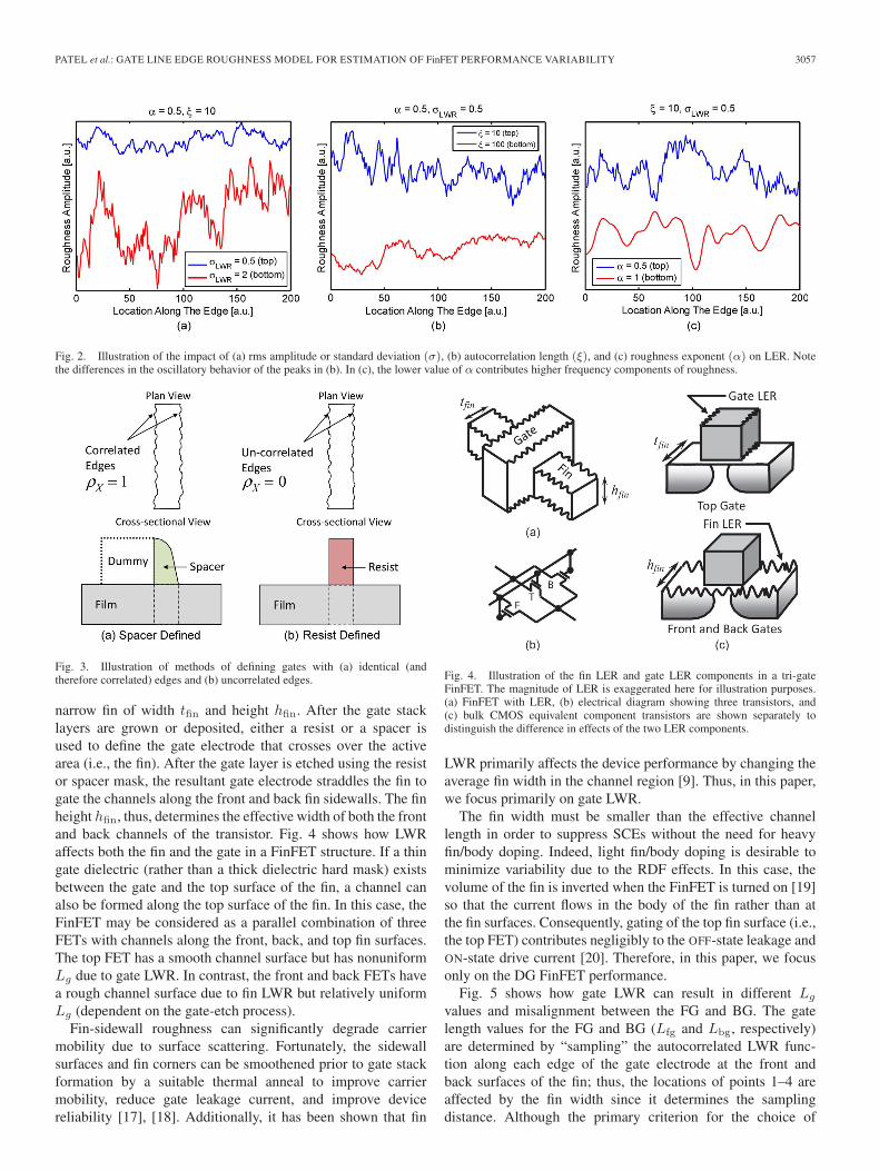
Fig. 2. Illustration of the impact of (a) rms amplitude or standard deviation (σ), (b) autocorrelation length (ξ), and (c) roughness exponent (α) on LER. Notethe differences in the oscillatory behavior of the peaks in (b). In (c), the lower value of α contributes higher frequency components of roughness.
Fig. 3. Illustration of methods of defining gates with (a) identical (andtherefore correlated) edges and (b) uncorrelated edges.
narrow fin of width tfin and height hfin. After the gate stacklayers are grown or deposited, either a resist or a spacer isused to define the gate electrode that crosses over the activearea (i.e., the fin). After the gate layer is etched using the resistor spacer mask, the resultant gate electrode straddles the fin togate the channels along the front and back fin sidewalls. The finheight hfin, thus, determines the effective width of both the frontand back channels of the transistor. Fig. 4 shows how LWRaffects both the fin and the gate in a FinFET structure. If a thingate dielectric (rather than a thick dielectric hard mask) existsbetween the gate and the top surface of the fin, a channel canalso be formed along the top surface of the fin. In this case, theFinFET may be considered as a parallel combination of threeFETs with channels along the front, back, and top fin surfaces.The top FET has a smooth channel surface but has nonuniformLg due to gate LWR. In contrast, the front and back FETs havea rough channel surface due to fin LWR but relatively uniformLg (dependent on the gate-etch process).
Fin-sidewall roughness can significantly degrade carriermobility due to surface scattering. Fortunately, the sidewallsurfaces and fin corners can be smoothened prior to gate stackformation by a suitable thermal anneal to improve carriermobility, reduce gate leakage current, and improve devicereliability [17], [18]. Additionally, it has been shown that fin
Fig. 4. Illustration of the fin LER and gate LER components in a tri-gateFinFET. The magnitude of LER is exaggerated here for illustration purposes.(a) FinFET with LER, (b) electrical diagram showing three transistors, and(c) bulk CMOS equivalent component transistors are shown separately todistinguish the difference in effects of the two LER components.
LWR primarily affects the device performance by changing theaverage fin width in the channel region [9]. Thus, in this paper,we focus primarily on gate LWR.
The fin width must be smaller than the effective channellength in order to suppress SCEs without the need for heavyfin/body doping. Indeed, light fin/body doping is desirable tominimize variability due to the RDF effects. In this case, thevolume of the fin is inverted when the FinFET is turned on [19]so that the current flows in the body of the fin rather than atthe fin surfaces. Consequently, gating of the top fin surface (i.e.,the top FET) contributes negligibly to the OFF-state leakage andON-state drive current [20]. Therefore, in this paper, we focusonly on the DG FinFET performance.
Fig. 5 shows how gate LWR can result in different Lg
values and misalignment between the FG and BG. The gatelength values for the FG and BG (Lfg and Lbg, respectively)are determined by “sampling” the autocorrelated LWR func-tion along each edge of the gate electrode at the front andback surfaces of the fin; thus, the locations of points 1–4 areaffected by the fin width since it determines the samplingdistance. Although the primary criterion for the choice of

3058 IEEE TRANSACTIONS ON ELECTRON DEVICES, VOL. 56, NO. 12, DECEMBER 2009
Fig. 5. Schematic views of a DG FinFET: (a) Top view of a FinFET. (b) Three-dimensional top view of a FinFET illustrating various gate electrode features.The FG and BG lengths and placements are defined by the points labeled 1–4,where the gate electrode wraps around the top of the fin.
TABLE ITWO-DIMENSIONAL DEVICE SIMULATION PARAMETERS
fin width (tfin) is SCE control, mitigation of the gate LWReffects to reduce variability may be an important secondaryconsideration.
As discussed earlier, spacer-defined lines have highly corre-lated edges so that gate length variations are negligible if spacerlithography is used to pattern the gate electrode. Nevertheless,the FG and BG can be misaligned. Thus, it is important to alsostudy the case where the FG and BG have the same gate lengthbut are offset by some distance.
If a highly anisotropic and uniform etch is used to form thegate electrode, the locations of points 1–4 (as determined bygate LWR and fin width) are transferred uniformly from the topof the fin to the bottom of the fin. In reality, the etch bias canvary from the top of the fin to the bottom of the fin, resultingin a tapered profile. The gate sidewall along the fin height mayhave a rough profile, and it has been shown that this behavioris adequately modeled by using the gate length that has beenaveraged along the height of the fin [9]. Moreover, the finitself can have a tapered profile; this has been studied by otherresearchers [21], [22]. These aforementioned nonidealities ofthe gate and fin profile are not considered in this paper.
B. Simulation Details
Table I lists the values of the process and device parame-ters that were used, generally following the ITRS HP 32-nmnode specifications. Fig. 6 shows the simulated 2-D devicestructure with FG and BG nonidealities. The source and draindoping profiles are Gaussian, peaked at the edges of the gate-sidewall spacers (defined by the implant baseline in Fig. 6),and assumed to have a lateral source/drain (S/D) doping gra-dient σS/D = 4 nm/dec [23]. This implant profile produces agate-underlapped S/D structure, which has been found to beoptimal for the sub-20-nm physical Lg regime [24]. Assuming
Fig. 6. Two-dimensional simulated device cross section of a DG FET struc-ture shown with nonidealities (misaligned and with gate length differencebetween the FG and BG).
an inversion carrier density of 1 × 1019 cm−3, the effectivegate length of the nominal device is 23.4 nm. Ideal metalliccontacts are made to the surfaces of the uniformly doped S/Dregions.
All simulations were performed using the Sentaurus devicesimulator [25], with coupled Poisson, quantum, and high-fieldsaturation models. In hydrodynamic (HD) simulations, the car-rier velocity is assumed to depend on the local carrier temper-ature, and, in the near-ballistic regime, it tends to overestimatethe velocity overshoot and drain current. In a study performedby Granzner et al. [26], it was found that, for 20-nm-gate-lengthDG devices, the ON-current and subthreshold leakage currentfrom the HD simulation were both overestimated by 80%compared to the MC simulation. In order to accurately relatethe simulation data to the experimentally determined valuesof ON-current and subthreshold leakage current, one would berequired to carefully calibrate the HD model parameters such asthe energy relaxation time (among other parameters). Nayfehand Antoniadis [27] calibrated the HD parameters using full-band MC simulation. In our simulation, we used the energyrelaxation time (τE) of 0.14 ps and energy flux parameter (rn)of 0.3 [23].
C. Model Formulation
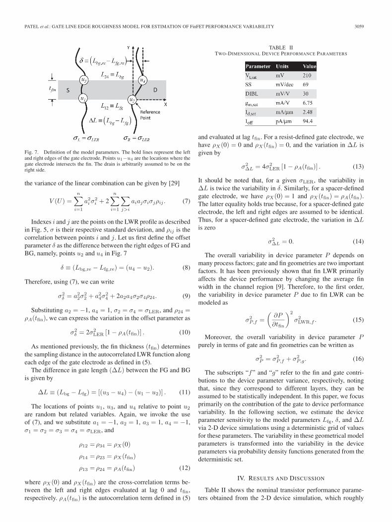
First, we formulate a simple statistical model to describethe variability in the geometrical parameters in terms of char-acteristic LWR descriptors. Consider the illustration in Fig. 7which describes the model parameters. Using point u2 as thereference, we need to describe the relationship of points u1, u3,and u4 in terms of characteristic LWR descriptors.
Misalignment between the FG and BG can occur due to thepresence of an offset (between points u1 and u3 and/or betweenpoints u2 and u4), with or without a difference in the gatecritical dimension of the FG and BG. Therefore, the geometrydepicted in Fig. 6 can alternately be described by our choiceof three parameters: FG length (Lfg), offset between FG andBG (δ), and gate length difference between FG and BG (ΔL).By definition, the variability in Lfg is identically equal to thelinewidth variability given by (4).
For any linear combination of n correlated Gaussian randomvariables
U =n∑
i=1
aiui (6)
PATEL et al.: GATE LINE EDGE ROUGHNESS MODEL FOR ESTIMATION OF FinFET PERFORMANCE VARIABILITY 3059
Fig. 7. Definition of the model parameters. The bold lines represent the leftand right edges of the gate electrode. Points u1−u4 are the locations where thegate electrode intersects the fin. The drain is arbitrarily assumed to be on theright side.
the variance of the linear combination can be given by [29]
V (U) =n∑
i=1
a2i σ
2i + 2
n∑i=1
∑j>i
aiajσiσjρij . (7)
Indexes i and j are the points on the LWR profile as describedin Fig. 5, σ is their respective standard deviation, and ρij is thecorrelation between points i and j. Let us first define the offsetparameter δ as the difference between the right edges of FG andBG, namely, points u2 and u4 in Fig. 7
δ ≡ (Lbg,re − Lfg,re) = (u4 − u2). (8)
Therefore, using (7), we can write
σ2δ = a2
2σ22 + a2
4σ24 + 2a2a4σ2σ4ρ24. (9)
Substituting a2 = −1, a4 = 1, σ2 = σ4 = σLER, and ρ24 =ρA(tfin), we can express the variation in the offset parameter as
σ2δ = 2σ2
LER [1 − ρA(tfin)] . (10)
As mentioned previously, the fin thickness (tfin) determinesthe sampling distance in the autocorrelated LWR function alongeach edge of the gate electrode as defined in (5).
The difference in gate length (ΔL) between the FG and BGis given by
ΔL ≡ (Lbg − Lfg) = [(u3 − u4) − (u1 − u2)] . (11)
The locations of points u1, u3, and u4 relative to point u2
are random but related variables. Again, we invoke the useof (7), and we substitute a1 = −1, a2 = 1, a3 = 1, a4 = −1,σ1 = σ2 = σ3 = σ4 = σLER, and
ρ12 = ρ34 = ρX(0)
ρ14 = ρ23 = ρX(tfin)
ρ13 = ρ24 = ρA(tfin) (12)
where ρX(0) and ρX(tfin) are the cross-correlation terms be-tween the left and right edges evaluated at lag 0 and tfin,respectively. ρA(tfin) is the autocorrelation term defined in (5)
TABLE IITWO-DIMENSIONAL DEVICE PERFORMANCE PARAMETERS
and evaluated at lag tfin. For a resist-defined gate electrode, wehave ρX(0) = 0 and ρX(tfin) = 0, and the variation in ΔL isgiven by
σ2ΔL = 4σ2
LER [1 − ρA(tfin)] . (13)
It should be noted that, for a given σLER, the variability inΔL is twice the variability in δ. Similarly, for a spacer-definedgate electrode, we have ρX(0) = 1 and ρX(tfin) = ρA(tfin).The latter equality holds true because, for a spacer-defined gateelectrode, the left and right edges are assumed to be identical.Thus, for a spacer-defined gate electrode, the variation in ΔLis zero
σ2ΔL = 0. (14)
The overall variability in device parameter P depends onmany process factors; gate and fin geometries are two importantfactors. It has been previously shown that fin LWR primarilyaffects the device performance by changing the average finwidth in the channel region [9]. Therefore, to the first order,the variability in device parameter P due to fin LWR can bemodeled as
σ2P,f =
(∂P
∂tfin
)2
σ2LWR,f . (15)
Moreover, the overall variability in device parameter Ppurely in terms of gate and fin geometries can be written as
σ2P = σ2
P,f + σ2P,g. (16)
The subscripts “f” and “g” refer to the fin and gate contri-butions to the device parameter variance, respectively, notingthat, since they correspond to different layers, they can beassumed to be statistically independent. In this paper, we focusprimarily on the contribution of the gate to device performancevariability. In the following section, we estimate the deviceparameter sensitivity to the model parameters Lfg, δ, and ΔLvia 2-D device simulations using a deterministic grid of valuesfor these parameters. The variability in these geometrical modelparameters is transformed into the variability in the deviceparameters via probability density functions generated from thedeterministic set.
IV. RESULTS AND DISCUSSION
Table II shows the nominal transistor performance parame-ters obtained from the 2-D device simulation, which roughly

3060 IEEE TRANSACTIONS ON ELECTRON DEVICES, VOL. 56, NO. 12, DECEMBER 2009
Fig. 8. Fin width dependence of the saturation threshold voltage. Vt,sat isdefined to be Vgs corresponding to 100-nA/μm Ids for Vds = 0.9 V.
Fig. 9. Fin width dependence of the saturation current and subthresholdleakage current.
matches the ITRS values for the 32-nm HP node [5]. Hereafter,the device parameters will be referenced to the nominal device,where no offset or gate length difference exists between the FGand BG. The saturation threshold voltage refers to the value ofVgs corresponding to 100 nA/μm for Vds = 0.9 V.
Let us first understand the fin LWR contribution to deviceparameter variability. The ITRS does not specify any LWRrequirements for the fin width [5]. We assume that the fin LWRbudget for the 32-nm node (7.5-nm fin width) is the same asthe gate LWR budget for the 18-nm node (7-nm physical gatelength). Thus, 3σLWR,f is assumed to be 1 nm. Fig. 8 showsthe fin width dependence of saturation threshold voltage. Itshould be noted that at ∼28 mV/nm, the threshold voltage isquite sensitive to the fin width thickness variation. Thus, using(15), the fin LWR is estimated to contribute ∼30 mV (3σ)to the total variation in Vt,sat. The fin width dependence ofsaturation current and subthreshold leakage current is shownin Fig. 9.
Among the gate resist requirements specified by the ITRSfor the 32-nm node, the allocated 3σ budget for low-frequencyLWR is 1.7 nm [5]. Although some measured LWR values havebeen reported [11], the values of the correlation length ξ androughness exponent α are largely unreported and/or have beenkept proprietary. As discussed earlier, the etch process acts as a
Fig. 10. Threshold voltage dependence on the CD difference ΔL and gateoffset δ assuming 13-nm FG length.
Fig. 11. Threshold voltage dependence on δ and ΔL. An FG length of 13 nmis assumed. The positive values of ΔL correspond to larger BG compared toFG, whereas the positive values of δ correspond to BG shifted more toward thedrain as compared to FG.
low-pass filter for LWR, and the lower values of α correspondto the high-frequency component in LWR. Therefore, unlessexplicitly mentioned, in this paper, we assume that α = 1which corresponds to an autocorrelation function as definedin (5).
Given the complex statistical nature of LWR, the MC ap-proach is an obvious choice. However, since MC TCAD simula-tions are computationally expensive and require a large numberof runs in each case to determine the statistical parameters withreasonable accuracy, we employed a methodology based onexperimental design techniques to eliminate the need for fullMC simulations.
First, we performed 2-D simulations for a predetermined setof values for Lfg, ΔL, and δ at 0.5-nm interval within the6-nm range (−3 to +3 nm) around their respective means. Thecomputational cost for the exploratory simulation of the threeaforementioned parameters is O(n3), where n is the numberof steps in each of the three parameter dimensions (Lfg, ΔL,and δ). The choice of 0.5-nm step size was based on a tradeoffbetween the TCAD computational time and the investigativerange of each parameter.
Fig. 10 shows a 3-D plot of the threshold voltage sensitivityto ΔL and δ for a device with nominal FG. When the BG issmaller than the FG, it can be seen from Fig. 11(a) that thethreshold voltage is lowered more for the BG shifted towardthe drain versus the BG shifted toward the source. This effect isreversed when the BG is larger than the FG. Another important

PATEL et al.: GATE LINE EDGE ROUGHNESS MODEL FOR ESTIMATION OF FinFET PERFORMANCE VARIABILITY 3061
Fig. 12. Comparison of the threshold voltage distributions obtained via directMC simulation and experimental grid for Lfg, ΔL, and δ. For the MCapproach, 2000 random values of Lfg, ΔL, and δ were generated and directlysimulated with Sentaurus. For the grid approach, the predetermined values ofLfg, ΔL, and δ at 0.5-nm spacing were simulated, and, then, random valueswere interpolated to this grid.
observation from Fig. 11(a) is that, for a given CD mismatchbetween the FG and BG, the FinFET threshold voltage isrelatively invariant over some range of the gate offset, whereas,as it can be seen in Fig. 11(b), even for no gate offset, thethreshold voltage is fairly sensitive to CD mismatch. Thus, theCD mismatch between the FG and BG is more critical thanthe gate offset.
By performing device simulation for this “grid,” we mappedout the variability space for the model parameters Lfg, ΔL,and δ. The computational efficiency of our approach is enabledby the structure of our model which parameterizes the FinFETstructure in terms of Lfg, ΔL, and δ and relates them tothe LWR descriptors ξ, σ, and α. Thus, any realization ofgate LWR is translated into the corresponding values of Lfg,ΔL, and δ, and the device performance can then be estimatedthrough straightforward interpolation using the presimulatedgrid. Thus, expensive TCAD simulations need to be performedonly once at each of the grid values, and, for any given setof LWR parameters (ξ, σ, and α), an MC experiment can beperformed outside of the TCAD environment (in any tool suchas MATLAB [30]). A lithography process engineer may needto evaluate several scenarios of LWR descriptors before settlingfor a given process. An accurate assessment of each scenariowould warrant a minimum of 200 MC runs. Thus, the initial“investment” of TCAD simulation is quickly paid off if manysuch scenarios need to be evaluated.
Using our MATLAB script (which accurately preserves allcorrelations), we generated 2000 MC samples of Lfg, ΔL, andδ. This MC set was directly simulated with Sentaurus; eachrun took approximately 200 s on 2-GHz quad CPU running64-b Linux. The same MC set was also approximated byinterpolation using the presimulated grid values. Interpolationin MATLAB was completed in less than 5 s. The resultingprobability density functions are compared in Fig. 12, and weconclude that our “grid” approach produces reasonably accu-rate results, combined with very good computational efficiency.For all subsequent analysis, the probability density functionfor each device parameter was approximated by interpolat-
Fig. 13. Variability in the saturation threshold voltage Vt,sat for a resist-defined gate electrode (a) as a function of LWR amplitude and (b) as a functionof correlation length. Note that the variability in Vt,sat is a much strongerfunction of the LWR amplitude than it is of the correlation length. The fin widthin both plots is 7.5 nm.
Fig. 14. Variability in the (filled symbols, left y-axis) saturation drive currentand (open symbols, right y-axis) OFF-state leakage current for a resist-definedgate electrode as a function of LWR amplitude. The fin width is 7.5 nm.
ing 10 000 values of Lfg, ΔL, and δ using the presimulatedbasis set.
Fig. 13 shows the impact of the LWR parameters σLWR
and ξ on the variability in the saturation threshold voltageVt,sat for a resist-defined gate electrode. An increase in σLWR
or a decrease in ξ each results in greater variation in δ and,hence, the effective channel length; thus, the variation in thethreshold voltage increases due to SCE. From Fig. 13(a), itshould be noted that, for the ITRS stipulated value of ∼1.7 nmfor 3σLWR, we observe a 21- to 30-mV variation (3σ) inVt,sat as compared to the 16-mV (1σ) variation reported dueto WFV [2]. Additionally, we observe that the Vt,sat sensitivityto σLWR ranges from 14 to 17 mV/nm. This is roughly halfcompared to the 28-mV/nm Vt,sat sensitivity to tfin variationobserved in Fig. 8. Thus, the fin width variation is the moresignificant component than gate LWR. The variability trendsfor Id,sat and log10(Ioff) are consistent with the trends observedfor Vt,sat, as shown in Figs. 14 and 15. Fig. 16 shows that thevariability in Vt,sat is further lowered when the gate electrodeis spacer-defined. In the spacer-defined case, σ2
LWR = 2σ2LER is
assumed. Consistent reductions in the variability were also seenfor Id,sat and log10(Ioff) (not shown).
It should be noted these trends observed for DG FinFETs incontrast with those reported for planar bulk MOSFETs [28].

3062 IEEE TRANSACTIONS ON ELECTRON DEVICES, VOL. 56, NO. 12, DECEMBER 2009
Fig. 15. Variability in the (filled symbols, left y-axis) saturation drive currentand (open symbols, right y-axis) OFF-state leakage current for a resist-definedgate electrode as a function of correlation length. The fin width is 7.5 nm.
Fig. 16. Comparison of variability in the saturation threshold voltage Vt,sat
for a resist-defined versus a spacer-defined gate electrode (a) as a function ofLWR amplitude for ξ = 10 nm and (b) as a function of correlation length forσ = 0.5 nm. The fin width in both plots is 7.5 nm.
Constantoudis and Gogolides [28] observed that a larger cor-relation length increased the threshold voltage variability and,thus, lowered the yield, defined by 10% tolerance. However, forFinFETs with either resist- or spacer-defined gate electrodes,an increase in the correlation length reduces the variationin Vt,sat.
V. CONCLUSION
The impact of gate LWR on FinFET performance variabilityis studied in this paper. Using a simple analytical model thatrelates LWR parameters to DG structure parameters, we wereable to gain physical insight into LWR and assess its impact onDG FET performance.
For any given LWR profile, we have shown that the frame-work presented in this paper can be used to assess the deviceperformance variability quickly without having the need toperform extensive MC TCAD simulations each time a newLWR profile needs to be investigated.
Furthermore, if a compact model for the DG FET were tobe developed and parameterized in terms of gate geometricalparameters Lfg, ΔL, and δ described in this paper, then, withthe aid of the variability equations presented in this paper, thevariability of any device parameter of interest can directly bederived.
ACKNOWLEDGMENT
The authors would like to thank Dr. L. Smith (Synopsys) forthe help with Sentaurus, the useful discussions, and bringing[27] to our attention; the anonymous reviewers for bringing [2]and [4] to our attention; and L. Sponton and Prof. M. Gastpar(UC Berkeley) for the helpful discussions. Kedar Patel wouldlike to thank L. Rowland and Dr. K. Quader at SanDisk forproviding the opportunity to conduct this work.
REFERENCES
[1] A. Asenov, A. R. Brown, J. H. Davies, S. Kaya, and G. Slavcheva,“Simulation of intrinsic parameter fluctuations in decananometer andnanometer-scale MOSFETs,” IEEE Trans. Electron Devices, vol. 50,no. 9, pp. 1837–1852, Sep. 2003.
[2] S. O’uchi, T. Matsukawa, T. Nakagawa, K. Endo, Y. X. Liu, T. Sekigawa,J. Tsukada, Y. Ishikawa, H. Yamauchi, K. Ishii, E. Suzuki,H. Koike, K. Sakamoto, and M. Masahara, “Characterization ofmetal-gate FinFET variability based on measurements and compactmodel analyses,” in IEDM Tech. Dig., San Francisco, CA, 2008, pp. 1–4.
[3] N. Lindert, L. Chang, Y.-K. Choi, E. H. Anderson, W.-C. Lee, T.-J. King,J. Bokor, and C. Hu, “Sub-60-nm quasi-planar FinFETs fabricated using asimplified process,” IEEE Electron Device Lett., vol. 22, no. 10, pp. 487–489, Oct. 2001.
[4] C. Gustin, L. H. A. Leunissen, A. Mercha, S. Decoutere, and G. Lorusso,“Impact of line width roughness on the matching performances of next-generation devices,” Thin Solid Films, vol. 516, no. 11, pp. 3690–3696,Apr. 2008.
[5] 2007 Edition International Technology Roadmap for Semiconductors.[Online]. Available: http://www.itrs.net
[6] T. Yoshimura, H. Shiraishi, J. Yamamoto, and S. Okazaki, “Nanoedgeroughness in polymer resist patterns,” Appl. Phys. Lett., vol. 63, no. 6,pp. 764–766, Aug. 1993.
[7] T. Yamaguchi, K. Yamazaki, M. Nagase, and H. Namatsu, “Line-edgeroughness: Characterization and material origin,” Jpn. J. Appl. Phys.,vol. 42, no. 6B, pp. 3755–3762, Jun. 2003.
[8] A. Asenov, S. Kaya, and A. R. Brown, “Intrinsic parameter fluctuations indecananometer MOSFETs introduced by gate line edge roughness,” IEEETrans. Electron Devices, vol. 50, no. 5, pp. 1254–1260, May 2003.
[9] E. Baravelli, M. Jurczak, N. Speciale, K. De Meyer, and A. Dixit, “Impactof LER and random dopant fluctuations on FinFET matching perfor-mance,” IEEE Trans. Nanotechnol., vol. 7, no. 3, pp. 291–298, May 2008.
[10] V. Constantoudis, G. P. Patsis, L. H. A. Leunissen, and E. Gogolides,“Line edge roughness and critical dimension variation: Fractal charac-terization and comparison using model functions,” J. Vac. Sci. Tech-nol. B, Microelectron. Process. Phenom., vol. 22, no. 4, pp. 1974–1981,Jul. 2004.
[11] V. Constantoudis, E. Gogolides, J. Roberts, and J. Stowers, “Characteriza-tion and modeling of line width roughness (LWR),” Proc. SPIE, vol. 5752,pp. 1227–1236, May 2005.
[12] G. Palasantzas, “Roughness spectrum and surface width of self-affinefractal surfaces via the K-correlation model,” Phys. Rev. B, Condens.Matter, vol. 48, no. 19, pp. 14 472–14 478, Nov. 1993.
[13] J. A. Croon, G. Storms, S. Winkelmeir, I. Pollentier, and M. Ercken,“Line edge roughness: Characterization, modeling and impact on devicebehavior,” in IEDM Tech. Dig., 2002, pp. 307–310.
[14] L. H. A. Leunissen, M. Ercken, M. Goethals, S. Locorotondo, andK. Ronse, “Transfer of line edge roughness during gate patterningprocesses,” in Proc. Int. Symp. Dry Process, 2004, vol. 4, pp. 1–6.
[15] P. Oldiges, Q. Lin, K. Pertillo, M. Sanchez, M. Ieong, and M. Hargrove,“Modeling line edge roughness effects in sub 100 nm gate length devices,”in Proc. SISPAD, 2000, pp. 131–134.
[16] L. Sponton, L. Bomholt, D. Pramanik, and W. Fichtner, “A full 3D TCADsimulation study of line-width roughness effects in 65 nm technology,” inProc. SISPAD, 2006, pp. 377–380.
[17] Y.-K. Choi, D. Ha, E. Snow, J. Bokor, and T.-J. King, “Reliability studyof CMOS FinFETs,” in IEDM Tech. Dig., 2003, pp. 177–180.
[18] W. Xiong, G. Gebara, J. Zaman, M. Gostkowski, B. Nguyen, G. Smith,D. Lewis, C. R. Cleavelin, R. Wise, S. Yua, M. Pas, T.-J. King, andJ. P. Colinge, “Improvement of FinFET electrical characteristics by hydro-gen annealing,” IEEE Electron Device Lett., vol. 25, no. 8, pp. 541–543,Aug. 2004.

PATEL et al.: GATE LINE EDGE ROUGHNESS MODEL FOR ESTIMATION OF FinFET PERFORMANCE VARIABILITY 3063
[19] L. Ge and J. Fossum, “Analytical modeling of quantization and volumeinversion in thin Si-film DG MOSFETs,” IEEE Trans. Electron Devices,vol. 49, no. 2, pp. 287–294, Feb. 2002.
[20] J. G. Fossum, L.-Q. Wang, J.-W. Yang, S.-H. Kim, and V. P. Trivedi,“Pragmatic design of nanoscale multi-gate CMOS,” in IEDM Tech. Dig.,2004, pp. 613–616.
[21] X. Wu, P. C. H. Chan, and M. Chan, “Impact of non-vertical sidewall onsub-50 nm FinFET,” in Proc. IEEE Int. SOI Conf., 2003, pp. 151–153.
[22] Y. Li and C.-H. Hwang, “Effect of fin angle on electrical characteristics ofnanoscale round-top-gate bulk FinFETs,” IEEE Trans. Electron Devices,vol. 54, no. 12, pp. 3426–3429, Dec. 2007.
[23] J.-W. Yang, P. M. Zeitzoff, and H.-H. Tseng, “Highly manufacturabledouble-gate FinFET with gate–source/drain underlap,” IEEE Trans. Elec-tron Devices, vol. 54, no. 6, pp. 1464–1470, Jun. 2007.
[24] S. Balasubramanian, L. Chang, B. Nikolic, and T.-J. King, “Circuit-performance implications for double-gate MOSFET scaling below25 nm,” in Proc. Silicon Nanoelectron. Workshop, 2003, pp. 16–17.
[25] Sentaurus TCAD User Manual, ver. Z-2007.03. [Online]. Available:http://www.synopsys.com/
[26] R. Granzner, V. M. Polyakov, F. Schwierz, M. Kittler, R. J. Luyken,W. Rosner, and M. Stadele, “Simulation of nanoscale MOSFETs usingmodified drift diffusion and hydrodynamic models and comparison withMonte Carlo results,” Microelectron. Eng., vol. 83, no. 2, pp. 241–246,Feb. 2006.
[27] O. M. Nayfeh and D. A. Antoniadis, “Calibrated hydrodynamic simula-tion of deeply-scaled well-tempered nanowire field effect transistors,” inProc. SISPAD, 2007, vol. 12, pp. 305–308.
[28] V. Constantoudis and E. Gogolides, “Correlation length and the problemof line width roughness,” Proc. SPIE, vol. 6518, p. 651 81N, Apr. 2005.
[29] G. E. P. Box, W. G. Hunter, and J. S. Hunter, Statistics for Experimenters.New York: Wiley, 1978, p. 87.
[30] The MathWorks Inc. [Online]. Available: http://www.mathworks.com
Kedar Patel (M’99–SM’08) received the B.S. de-gree (magna cum laude) in engineering physics andthe M.S. degree in electrical engineering from theUniversity of California, Berkeley, in 1997 and 1998,respectively, where he is currently working towardthe Ph.D. degree.
In the past ten years, he has primarily worked ontechnology development and process integration. AtCypress Semiconductor, he worked on developingthree generations of SRAM technologies and trans-ferring them to production in Bloomington, MN.
While at PDF Solutions, he consulted U.S. and European clients on logic andembedded DRAM and Flash-memory-related yield issues. At Matrix Semicon-ductor (now SanDisk Corporation), Milpitas, CA, he worked on technologydevelopment of three generations of a revolutionary 3-D (multilayered) one-time-programmable memory using industry standard semiconductor materialsand processes, where he is currently managing the product engineering teamthat is responsible for SSD and 3-D products. His current research interests arein understanding the impact of intrinsic process variations on devices, as wellas novel approaches to quantify their impact on circuit performance. He is theholder of two patents in process technology.
Tsu-Jae King Liu (F’07) received the B.S., M.S.,and Ph.D. degrees in electrical engineering fromStanford University, Stanford, CA, in 1984, 1986,and 1994, respectively.
In 1992, she joined the Xerox Palo Alto ResearchCenter as a Member of the research staff to researchand develop polycrystalline silicon thin-film tran-sistor technologies for high-performance flat-paneldisplay and imaging applications. In August 1996,she joined the faculty of the University of California,Berkeley, where she is currently a Professor of elec-
trical engineering and computer sciences and the Associate Dean for Researchwith the College of Engineering. Her research activities are currently innanometer-scale logic and memory devices and technology. She has authoredor coauthored over 300 publications and is the holder of over 60 U.S. patents.
Dr. Liu has served on several committees for many technical conferences,including the International Electron Devices Meeting and the Symposium onVLSI Technology, and was a member of the IEEE EDS VLSI Technology andCircuits Technical Committee. From 1999 to 2004, she served as an Editor forthe IEEE ELECTRON DEVICE LETTERS. She was the recipient of the DARPASignificant Technical Achievement Award (2000) for the development of theFinFET, the Electrical Engineering Award for Outstanding Teaching at UCBerkeley (2003), and the NAE Lillian M. Gilbreth Lectureship (2006).
Costas J. Spanos (M’77–SM’96–F’00) received theB.E.E. degree (with honors) from the National Tech-nical University of Athens, Athens, Greece, in 1980and the M.S. and Ph.D. degrees in electrical andcomputer engineering from Carnegie Mellon Univer-sity, Pittsburgh, PA, in 1981 and 1985, respectively.
From 1985 to 1988, he was with the AdvancedComputer-Aided Design Group, Digital EquipmentCorporation, Hudson, MA, where he worked on thestatistical characterization, simulation, and diagnosisof VLSI processes. In 1988, he joined the faculty of
the Department of Electrical Engineering and Computer Sciences (EECS De-partment), University of California, Berkeley, where he is currently a Professor.From 1994 to 2000, he was the Director with the Berkeley MicrofabricationLaboratory, and, from 2004 to 2005, he was the Director with the ElectronicsResearch Laboratory, and, from 2004 to 2008, he was the Associate Dean forResearch with the College of Engineering. He is currently the Associate Chairof the EECS Department and the Chair of the EE Division. He has publishedmore than 200 referred articles, has received several best paper awards, and hascoauthored a textbook in semiconductor manufacturing. From 1998 to 2003, heled a multicampus multi-PI research project on small feature reproducibility.His current research interests include the development of flexible manufactur-ing systems, the application of statistical analysis in the design and fabricationof integrated circuits, and the development and deployment of novel sensorsand computer-aided techniques in semiconductor manufacturing.
Prof. Spanos has served in the technical committees of the IEEE Symposiumon VLSI Technology, the International Semiconductor Manufacturing SciencesSymposium, the Advanced Semiconductor Manufacturing Symposium, and theInternational Workshop on Statistical Metrology, and he was the Editor of theIEEE TRANSACTIONS ON SEMICONDUCTOR MANUFACTURING from 1991to 1994.