gan wideband 10 w cw / pulsed transistor in plastic ... · pdf filegan wideband 10 w cw /...
TRANSCRIPT

GaN Wideband 10 W CW / Pulsed Transistor in Plastic Package DC - 3.5 GHz
Rev. V1
MAGX-000035-01000P
1 1 1
M/A-COM Technology Solutions Inc. (MACOM) and its affiliates reserve the right to make changes to the product(s) or information contained herein without notice. Visit www.macomtech.com for additional data sheets and product information.
• North America Tel: 800.366.2266 / Fax: 978.366.2266 • Europe Tel: 44.1908.574.200 / Fax: 44.1908.574.300 • Asia/Pacific Tel: 81.44.844.8296 / Fax: 81.44.844.8298
Features
GaN on SiC D-Mode Transistor Technology
Unmatched, Ideal for Pulsed / CW Applications
50 V Typical Bias, Class AB
Common-Source Configuration
Thermally-Enhanced 3 x 6 mm 14-Lead DFN
MTTF = 600 years (TJ < 200°C)
Halogen-Free “Green” Mold Compound
RoHS* Compliant and 260°C Reflow Compatible
MSL-1
Description
The MAGX-000035-01000P is a GaN on SiC unmatched power device offering the widest RF frequency capability, most reliable high voltage operation, lowest overall power transistor size, cost and weight in a “TRUE SMT” plastic-packaging technology. Use of an internal stress buffer technology allows reliable operation at junction temperatures up to 200°C. The small package size and excellent RF performance make it an ideal replacement for costly flanged or metal-backed module components.
Ordering Information1,2
* Restrictions on Hazardous Substances, European Union Directive 2002/95/EC.
1. Reference Application Note M513 for reel size information. 2. When ordering sample evaluation boards, choose a standard
frequency range indicated on page 4/5 or specify a desired custom range. Custom requests may increase lead times.
Part Number Package
MAGX-000035-01000P Bulk Packaging
MAGX-000035-0100TP 500 Piece Reel
MAGX-000035-PB4PPR Sample Board
Functional Schematic
Pin Configuration3
Pin No. Function Pin No. Function
1 No Connection 8 No Connection
2 No Connection 9 No Connection
3 VGG/RFIN 10 VDD/RFOUT
4 VGG/RFIN 11 VDD/RFOUT
5 VGG/RFIN 12 VDD/RFOUT
6 No Connection 13 No Connection
7 No Connection 14 No Connection
15 Paddle4
3. MACOM recommends connecting unused package pins to ground.
4. The exposed pad centered on the package bottom must be connected to RF and DC ground.
NC NC NC NC
NC NC NC NC
1 2 3 4 5 6 7
14 13 12 11 10 9 8
15
G GG
DD D

GaN Wideband 10 W CW / Pulsed Transistor in Plastic Package DC - 3.5 GHz
Rev. V1
MAGX-000035-01000P
2 2 2
M/A-COM Technology Solutions Inc. (MACOM) and its affiliates reserve the right to make changes to the product(s) or information contained herein without notice. Visit www.macomtech.com for additional data sheets and product information.
• North America Tel: 800.366.2266 / Fax: 978.366.2266 • Europe Tel: 44.1908.574.200 / Fax: 44.1908.574.300 • Asia/Pacific Tel: 81.44.844.8296 / Fax: 81.44.844.8298
Parameter Test Conditions Symbol Min. Typ. Max. Units
DC CHARACTERISTICS
Drain-Source Leakage Current VGS = -8 V, VDS = 175 V IDS - - 1.0 mA
Gate Threshold Voltage VDS = 5 V, ID = 2 mA VGS (th) -5 -3 -2 V
Forward Transconductance VDS = 5 V, ID = 250 mA GM 0.20 - - S
DYNAMIC CHARACTERISTICS
Input Capacitance VDS = 0 V, VGS = -8 V, F = 1 MHz CISS - 2.2 - pF
Output Capacitance VDS = 50 V, VGS = -8 V, F = 1 MHz COSS - 0.9 - pF
Reverse Transfer Capacitance VDS = 50 V, VGS = -8 V, F = 1 MHz CRSS - 0.1 - pF
Electrical Characteristics: TA = 25°C
Electrical Specifications5: Freq. = 1.6 GHz, TA = 25°C, Z0 = 50 Ω
Parameter Symbol Min. Typ. Max. Units
CW RF FUNCTIONAL TESTS: VDD = 50 V, IDQ = 30 mA, P2.5 dB
CW Output Power POUT - 10 - W
Pulsed RF FUNCTIONAL TESTS: VDD = 50 V, IDQ = 30 mA, P2.5 dB, Pulse Width = 1 ms, Duty Cycle = 10%
Pulsed Output Power POUT 9.2 10.6 - W
Pulsed Power Gain GP 14.2 14.8 - dB
Pulsed Drain Efficiency ηD 55 58 - %
Load Mismatch Stability VSWR-S - 5:1 - -
Load Mismatch Tolerance VSWR-T - 10:1 - -
Typical Performance: VDD = 50 V, IDQ = 30 mA, TA = 25°C
Parameter 30 MHz 1 GHz 2.5 GHz 3.5 GHz Units
Gain 17 15 14 14 dB
Saturated Power (PSAT) 13 11 10 10 W
Power Gain at PSAT 15 14 13 12 dB
PAE @ PSAT 65 55 53 50 %
5. Electrical specifications measured in MACOM RF evaluation boards. See recommended tuning solutions on page 4.

GaN Wideband 10 W CW / Pulsed Transistor in Plastic Package DC - 3.5 GHz
Rev. V1
MAGX-000035-01000P
3 3 3
M/A-COM Technology Solutions Inc. (MACOM) and its affiliates reserve the right to make changes to the product(s) or information contained herein without notice. Visit www.macomtech.com for additional data sheets and product information.
• North America Tel: 800.366.2266 / Fax: 978.366.2266 • Europe Tel: 44.1908.574.200 / Fax: 44.1908.574.300 • Asia/Pacific Tel: 81.44.844.8296 / Fax: 81.44.844.8298
Parameter Absolute Max.
Input Power POUT - GP + 2.5 dBm
Drain Supply Voltage, VDD +65 V
Gate Supply Voltage, VGG -8 V to 0 V
Supply Current, IDD 500 mA
Power Dissipation, CW @ 85ºC 12 W
Power Dissipation (PAVG), Pulsed @ 85°C 12 W
Junction Temperature11 200°C
Operating Temperature -40°C to +95°C
Storage Temperature -65°C to +150°C
ESD Maximum - Human Body Model (HBM) 400 V
ESD Maximum - Charged Device Model (CDM) 150 V
Absolute Maximum Ratings 6,7,8,9,10
6. Exceeding any one or combination of these limits may cause permanent damage to this device. 7. MACOM does not recommend sustained operation near these survivability limits. 8. For saturated performance it is recommended that the sum of (3 * VDD + abs (VGG)) < 175 V. 9. CW operation at VDD voltages above 50 V is not recommended. 10. Operating at nominal conditions with TJ ≤ 200°C will ensure MTTF > 1 x 10⁶ hours. Junction temperature
directly affects device MTTF and should be kept as low as possible to maximize lifetime. 11. Junction Temperature (TJ) = TC + ӨJC * ((V * I) - (POUT - PIN)) Typical CW thermal resistance (ӨJC) = 5.8°C/W a) For TC = 83°C, TJ = 124°C @ 50 V, 330 mA, POUT = 10W, PIN = 0.6W Typical transient thermal resistances: b) 300 µs pulse, 10% duty cycle, ӨJC = 1.94°C/W For TC = 83°C, TJ = 97°C @ 50 V, 325mA, POUT = 9.8W, PIN = 0.6 W c) 1 ms pulse, 10% duty cycle, ӨJC = 2.01°C/W For TC = 83°C, TJ = 98°C @ 50 V, 325mA, POUT = 9.8W, PIN = 0.6W d) 1 ms pulse, 20% duty cycle, ӨJC = 2.56°C/W For TC = 83°C, TJ = 101°C @ 50 V, 325 mA, POUT = 9.8 W, PIN = 0.6 W

GaN Wideband 10 W CW / Pulsed Transistor in Plastic Package DC - 3.5 GHz
Rev. V1
MAGX-000035-01000P
4 4 4
M/A-COM Technology Solutions Inc. (MACOM) and its affiliates reserve the right to make changes to the product(s) or information contained herein without notice. Visit www.macomtech.com for additional data sheets and product information.
• North America Tel: 800.366.2266 / Fax: 978.366.2266 • Europe Tel: 44.1908.574.200 / Fax: 44.1908.574.300 • Asia/Pacific Tel: 81.44.844.8296 / Fax: 81.44.844.8298
Parts List (N/A = not applicable for this tuning solution)
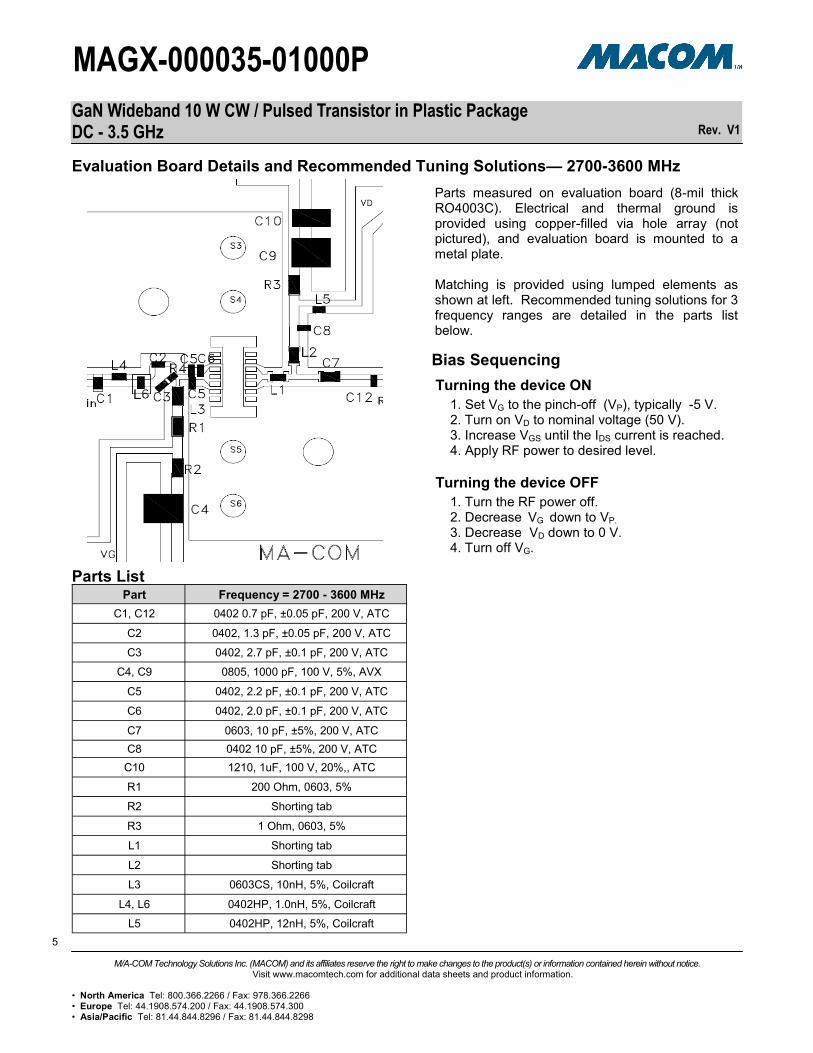
Parts measured on evaluation board (8-mil thick RO4003C). Electrical and thermal ground is provided using copper-filled via hole array (not pictured), and evaluation board is mounted to a metal plate. Matching is provided using lumped elements as shown at left. Recommended tuning solutions for 3 frequency ranges are detailed in the parts list below.
Evaluation Board Details and Recommended Tuning Solutions
Turning the device ON
1. Set VG to the pinch-off (VP), typically -5 V. 2. Turn on VD to nominal voltage (50 V). 3. Increase VGS until the IDS current is reached. 4. Apply RF power to desired level.
Turning the device OFF
1. Turn the RF power off. 2. Decrease VG down to VP. 3. Decrease VD down to 0 V. 4. Turn off VG.
Bias Sequencing
Part Frequency = 900-1400 MHz Frequency = 1600 MHz Frequency = 1625-1675 MHz
C1 0402, 6.8 pF, ±5%, 200V ATC 0402, 4.7 pF, ±0.1pF, 200 V, ATC 0402, 3.3 pF, ±0.1pF, 200 V, ATC
C2 0603, 6.8 pF, ±0.1 pF, 250 V, ATC 0603, 8.2 pF, ±0.1 pF, 250 V, ATC 0603, 8.2 pF, ±0.1 pF, 250 V, ATC
C3 0603, 82 pF, ±10%, 250 V, ATC 0603, 68 pF, ±10%, 250 V, ATC 0603, 68 pF, ±10%, 250 V, ATC
C4 0805, 1000 pF, 100 V, 5%, AVX 0805, 1000 pF, 100 V, 5%, AVX 0805, 1000 pF, 100 V, 5%, AVX
C5 N/A 0603, 1.5 pF, ±0.1 pF, 250 V, ATC N/A
C6 N/A N/A 0603, 1.5 pF, ±0.1 pF, 250 V, ATC
C7 0603, 39 pF, ±10%, 250 V, ATC 0603, 20 pF, ±10% pF, 250 V, ATC 0603, 20 pF, ±10% pF, 250 V, ATC
C8 0603, 82 pF, ±10%, 250 V, ATC 0603, 68 pF, ±10%, 250 V, ATC 0603, 68 pF, ±10%, 250 V, ATC
C9 0805, 1000 pF, 100 V, 5%, AVX 0805, 1000 pF, 100 V, 5%, AVX 0805, 1000 pF, 100 V, 5%, AVX
C10 0805, 1000 pF, 100 V, 5%, AVX 0805, 1000 pF, 100 V, 5%, AVX 0805, 1000 pF, 100 V, 5%, AVX
C11 N/A N/A N/A
C12 N/A 0603, 10 pF, ±0.1 pF, 250 V, ATC 0603, 6.8 pF, ±0.1 pF, 250 V, ATC
R1 240 Ω, 0603, 5% 200 Ω, 0603, 5% 200 Ω, 0603, 5%
R2 1.0 Ω, 0603, 5% 1.0 Ω, 0603, 5% 1.0 Ω, 0603, 5%
R3 1.0 Ω, 0603, 5% 1.0 Ω, 0603, 5% 1.0 Ω, 0603, 5%
R4 8.2 Ω, 0603, 5% 33 Ω, 0603, 5% 75 Ω, 0603, 5%
L1 0402HP, 3.3 nH, 5%, Coilcraft 0402HP, 2.7 nH, 5%, Coilcraft Shorting tab
L2 0603HP, 6.8 nH, 5%, Coilcraft 0603HP, 1.6 nH, 5%, Coilcraft 0603HP, 1.6 nH, 5%, Coilcraft
L3 0402CS, 4.3 nH, 5%, Coilcraft 0402HP, 2.7 nH, 5%, Coilcraft 0402HP, 2.7 nH, 5%, Coilcraft
L4 0402CS, 3.3nH 5% (900-1300MHz); or
2.4nH, 5% for 1000MHz-1400MHz, Coilcraft 0402HP, 2.7 nH, 5%, Coilcraft 0402HP, 2.7 nH, 5%, Coilcraft
GaN Wideband 10 W CW / Pulsed Transistor in Plastic Package DC - 3.5 GHz
Rev. V1
MAGX-000035-01000P
5 5 5
M/A-COM Technology Solutions Inc. (MACOM) and its affiliates reserve the right to make changes to the product(s) or information contained herein without notice. Visit www.macomtech.com for additional data sheets and product information.
• North America Tel: 800.366.2266 / Fax: 978.366.2266 • Europe Tel: 44.1908.574.200 / Fax: 44.1908.574.300 • Asia/Pacific Tel: 81.44.844.8296 / Fax: 81.44.844.8298
Parts List
Parts measured on evaluation board (8-mil thick RO4003C). Electrical and thermal ground is provided using copper-filled via hole array (not pictured), and evaluation board is mounted to a metal plate. Matching is provided using lumped elements as shown at left. Recommended tuning solutions for 3 frequency ranges are detailed in the parts list below.
Evaluation Board Details and Recommended Tuning Solutions— 2700-3600 MHz
Turning the device ON
1. Set VG to the pinch-off (VP), typically -5 V. 2. Turn on VD to nominal voltage (50 V). 3. Increase VGS until the IDS current is reached. 4. Apply RF power to desired level.
Turning the device OFF
1. Turn the RF power off. 2. Decrease VG down to VP. 3. Decrease VD down to 0 V. 4. Turn off VG.
Bias Sequencing
Part Frequency = 2700 - 3600 MHz
C1, C12 0402 0.7 pF, ±0.05 pF, 200 V, ATC
C2 0402, 1.3 pF, ±0.05 pF, 200 V, ATC
C3 0402, 2.7 pF, ±0.1 pF, 200 V, ATC
C4, C9 0805, 1000 pF, 100 V, 5%, AVX
C5 0402, 2.2 pF, ±0.1 pF, 200 V, ATC
C6 0402, 2.0 pF, ±0.1 pF, 200 V, ATC
C7 0603, 10 pF, ±5%, 200 V, ATC
C8 0402 10 pF, ±5%, 200 V, ATC
C10 1210, 1uF, 100 V, 20%,, ATC
R1 200 Ohm, 0603, 5%
R2 Shorting tab
R3 1 Ohm, 0603, 5%
L1 Shorting tab
L2 Shorting tab
L3 0603CS, 10nH, 5%, Coilcraft
L4, L6 0402HP, 1.0nH, 5%, Coilcraft
L5 0402HP, 12nH, 5%, Coilcraft

GaN Wideband 10 W CW / Pulsed Transistor in Plastic Package DC - 3.5 GHz
Rev. V1
MAGX-000035-01000P
6 6 6
M/A-COM Technology Solutions Inc. (MACOM) and its affiliates reserve the right to make changes to the product(s) or information contained herein without notice. Visit www.macomtech.com for additional data sheets and product information.
• North America Tel: 800.366.2266 / Fax: 978.366.2266 • Europe Tel: 44.1908.574.200 / Fax: 44.1908.574.300 • Asia/Pacific Tel: 81.44.844.8296 / Fax: 81.44.844.8298
Handling Procedures
Please observe the following precautions to avoid damage:
Static Sensitivity
Gallium Nitride Devices and Circuits are sensitive to electrostatic discharge (ESD) and can be damaged by static electricity. Proper ESD control techniques should be used when handling these Class 1A devices.
Lead-Free 3x6 mm 14-Lead DFN†
† Reference Application Note S2083 for lead-free solder reflow
recommendations. Meets JEDEC moisture sensitivity level 1 requirements. Plating is Ni/Pd/Au.

GaN Wideband 10 W CW / Pulsed Transistor in Plastic Package DC - 3.5 GHz
Rev. V1
MAGX-000035-01000P
7 7 7
M/A-COM Technology Solutions Inc. (MACOM) and its affiliates reserve the right to make changes to the product(s) or information contained herein without notice. Visit www.macomtech.com for additional data sheets and product information.
• North America Tel: 800.366.2266 / Fax: 978.366.2266 • Europe Tel: 44.1908.574.200 / Fax: 44.1908.574.300 • Asia/Pacific Tel: 81.44.844.8296 / Fax: 81.44.844.8298
Applications Section
Power (Output & Dissipated) and Transient Junction Temperature vs. Pulse Duration and Duty Cycle
Thermal Performance: Freq. = 1200 MHz, TC = 85°C, VDD = +50 V, IDQ = 30 mA, Z0 = 50 Ω
Junction temperature measured using High-Speed Transient (HST) temperature detection microscopy.
Pulse Width, 100 µs,
10%
100 µs,
20%
300 µs,
10%
300 µs,
20%
500 µs,
10%
500 µs,
20%
1000 µs,
10%
1000 µs,
20%
8000 µs,
9.2% Duty Cycle
Power Dissipation (W) 6.8 7.1 6.9 7.1 6.9 7.1 6.9 7.1 7.0
1.2 GHz POUT (W) 9.79 9.75 9.75 9.75 9.75 9.75 9.75 9.75 9.90
Max. Transient Junction Temp. (oC)
92.5 93.1 97.3 96.7 98.3 98.5 97.8 102.2 100.7
90
92
94
96
98
100
102
104
5
6
7
8
9
10
11
100 µ
s,
10%
100 µ
s,2
0%
300 µ
s,1
0%
300 µ
s,2
0%
500 µ
s,1
0%
500 µ
s,2
0%
1000 µ
s,1
0%
1000 µ
s,2
0%
8000 µ
s,9
.2%
Tra
ns
ien
t J
un
cti
on
Te
mp
era
ture
( C
)
Po
we
r O
utp
ut
(W)
an
d D
iss
ipa
ted
(W
)
Pulse Width (µs), Duty Cycle (%)
Dissipated Power
Output Power
Max. Transient Junction Temp.

GaN Wideband 10 W CW / Pulsed Transistor in Plastic Package DC - 3.5 GHz
Rev. V1
MAGX-000035-01000P
8 8 8
M/A-COM Technology Solutions Inc. (MACOM) and its affiliates reserve the right to make changes to the product(s) or information contained herein without notice. Visit www.macomtech.com for additional data sheets and product information.
• North America Tel: 800.366.2266 / Fax: 978.366.2266 • Europe Tel: 44.1908.574.200 / Fax: 44.1908.574.300 • Asia/Pacific Tel: 81.44.844.8296 / Fax: 81.44.844.8298
Applications Section
Power Gain vs. Frequency
Output Power vs. Frequency Drain Efficiency vs. Frequency
Typical Pulsed Performance Curves (reference 900 MHz - 1400 MHz parts list, L4 = 2.4 nH): 900 - 1400 MHz, 200 µs Pulse, 20% Duty Cycle, PIN = 0.5 W, VDD= +50 V, TA = 25°C, Z0 = 50 Ω
Input Return Loss vs. Frequency
Pulse Droop vs. Frequency Output Drive & Power Gain vs. Input Power
10
12
14
16
18
20
22
2
4
6
8
10
12
14
0.0 0.2 0.4 0.6 0.8 1.0
Po
we
r G
ain
(d
B)
Ou
tpu
t P
ow
er (W
pk
)
Input Power (Wpk)900MHz_P 1200MHz_P 1300MHz_P 1400MHz_P
900MHz_G 1200MHz_G 1300MHz_G 1400MHz_G
-25
-20
-15
-10
-5
0
900 1000 1100 1200 1300 1400
S11 (d
B)
Frequency (MHz)
0.00
0.02
0.04
0.06
0.08
0.10
900 1000 1100 1200 1300 1400
Pu
lse D
roo
p (
dB
)
Frequency (MHz)
10
11
12
13
14
15
900 1000 1100 1200 1300 1400
Po
wer
Gain
(d
B)
Frequency (MHz)
10
11
12
13
14
15
900 1000 1100 1200 1300 1400
Ou
tpu
t P
ow
er
(Wp
k)
Frequency (MHz)
50
54
58
62
66
70
900 1000 1100 1200 1300 1400
Dra
in E
ffic
ien
cy (
%)
Frequency (MHz)
GaN Wideband 10 W CW / Pulsed Transistor in Plastic Package DC - 3.5 GHz
Rev. V1
MAGX-000035-01000P
9 9 9
M/A-COM Technology Solutions Inc. (MACOM) and its affiliates reserve the right to make changes to the product(s) or information contained herein without notice. Visit www.macomtech.com for additional data sheets and product information.
• North America Tel: 800.366.2266 / Fax: 978.366.2266 • Europe Tel: 44.1908.574.200 / Fax: 44.1908.574.300 • Asia/Pacific Tel: 81.44.844.8296 / Fax: 81.44.844.8298
Applications Section
Power Gain vs. Input Power
Output Power vs. Input Power Drain Efficiency vs. Input Power
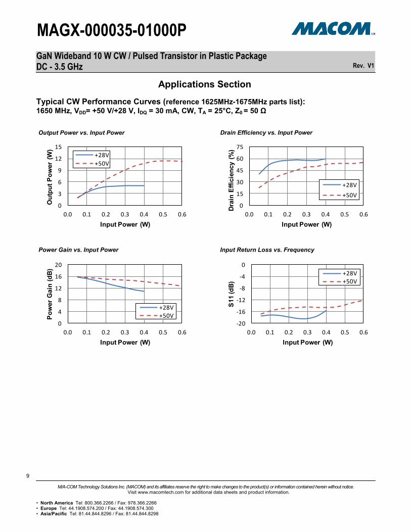
Typical CW Performance Curves (reference 1625MHz-1675MHz parts list): 1650 MHz, VDD= +50 V/+28 V, IDQ = 30 mA, CW, TA = 25°C, Z0 = 50 Ω
Input Return Loss vs. Frequency
0
15
30
45
60
75
0.0 0.1 0.2 0.3 0.4 0.5 0.6
Dra
in E
ffic
ien
cy (
%)
Input Power (W)
+28V
+50V
0
3
6
9
12
15
0.0 0.1 0.2 0.3 0.4 0.5 0.6
Ou
tpu
t P
ow
er
(W)
Input Power (W)
+28V
+50V
0
4
8
12
16
20
0.0 0.1 0.2 0.3 0.4 0.5 0.6
Po
wer
Gain
(d
B)
Input Power (W)
+28V+50V
-20
-16
-12
-8
-4
0
0.0 0.1 0.2 0.3 0.4 0.5 0.6
S11 (d
B)
Input Power (W)
+28V+50V
GaN Wideband 10 W CW / Pulsed Transistor in Plastic Package DC - 3.5 GHz
Rev. V1
MAGX-000035-01000P
10 10 10
M/A-COM Technology Solutions Inc. (MACOM) and its affiliates reserve the right to make changes to the product(s) or information contained herein without notice. Visit www.macomtech.com for additional data sheets and product information.
• North America Tel: 800.366.2266 / Fax: 978.366.2266 • Europe Tel: 44.1908.574.200 / Fax: 44.1908.574.300 • Asia/Pacific Tel: 81.44.844.8296 / Fax: 81.44.844.8298
Applications Section
Power Gain vs. Frequency
Output Power vs. Frequency Drain Efficiency vs. Frequency
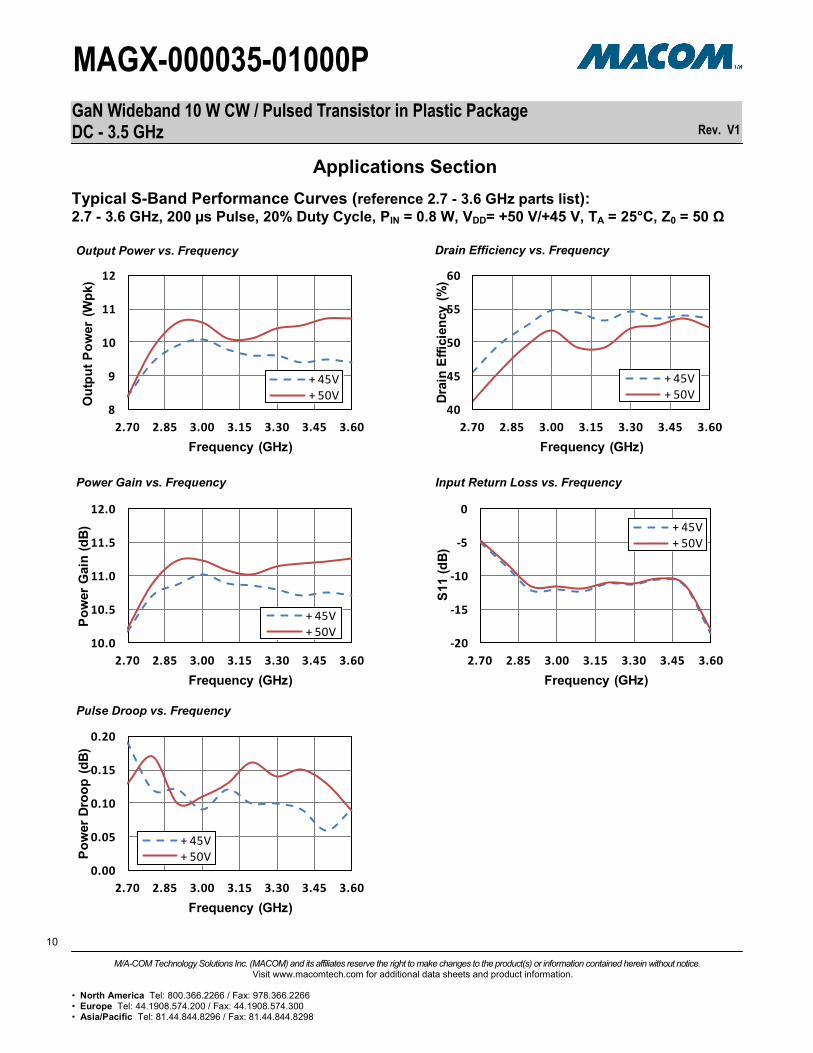
Typical S-Band Performance Curves (reference 2.7 - 3.6 GHz parts list): 2.7 - 3.6 GHz, 200 µs Pulse, 20% Duty Cycle, PIN = 0.8 W, VDD= +50 V/+45 V, TA = 25°C, Z0 = 50 Ω
Input Return Loss vs. Frequency
Pulse Droop vs. Frequency
-20
-15
-10
-5
0
2.70 2.85 3.00 3.15 3.30 3.45 3.60
S11 (
dB
)
Frequency (GHz)
+ 45V+ 50V
0.00
0.05
0.10
0.15
0.20
2.70 2.85 3.00 3.15 3.30 3.45 3.60
Po
wer
Dro
op
(d
B)
Frequency (GHz)
+ 45V+ 50V
8
9
10
11
12
2.70 2.85 3.00 3.15 3.30 3.45 3.60
Ou
tpu
t P
ow
er
(Wp
k)
Frequency (GHz)
+ 45V+ 50V
40
45
50
55
60
2.70 2.85 3.00 3.15 3.30 3.45 3.60D
rain
Eff
icie
ncy (
%)
Frequency (GHz)
+ 45V+ 50V
10.0
10.5
11.0
11.5
12.0
2.70 2.85 3.00 3.15 3.30 3.45 3.60
Po
wer
Gain
(d
B)
Frequency (GHz)
+ 45V+ 50V