gaas fet pre amp cookbook #3 kent britain wa5 vjb fet pre amp cookbook #3 kent britain wa5 ......
TRANSCRIPT

GaAs FET Pre Amp Cookbook #3Kent Britain WA5 VJB
There are many designs for building preamps. each with their own advantages anddisadvantages. By putting together aninput, bias, powersupply, and output, you can optimize apreamp for your station. My thanks to W5ETG, N5QGH, and AASC for their help.
Inputs: The input network transforms 50 Ohms to the input impedance ofthe GaAs FET. AlVHF a typical GaAs FET has about a 3000 Ohms input impedance. A High Q circuit is usuallyused to transform the impedance up and at the sametime filter out unwanted signals.As frequency increases. the GaAs FET input impedance drops to a few dozen ohms at 10 GHz.HEMT's have an even higher input impedance, almost 5000 Ohms at VHF, dropping 10 50 Ohmsat I I GHz. Here we will talk about I I common input circuits.
#1Advantages: Low Pans Count
Low loss
Disadvantages: Optimal noise match isa matter of luck.
INPUT'_ "*'-1--Y-j
This is one of the simplest input circuits and works nicely up to 1296 MHz. A true match from 50 Ohmsto the Gamma opt.or best Noise Figure conditionforyour GaAs FET depends onthe stray capacitancefrom theGate to Ground.
#2Advantages: Optimum match
Variable Q (See tuning)
Disadvantages: Needs two high quality trimmersTuning interacts
INPUT_ "*"-r''rt--I
This is the most popular inputcircuit forhigh performance preamps below500 MHz. Due to the highinput impedance afthe GaAs FET below sao MHz the Q orBandwidth af the inputcircuit can be variedwith little cost to Noise Figure. Seethe Tuning Tipsdiagram.
3INPUT
#3Advantages: Extremely low loss
Input is at DC Ground
Disadvantages: Extremely wide BandwidthOnly matches low impedanceGaAs FET's MGFISOI, 2116 etc,
Limited 10 50, 144, and 222 MHz
The tapped L input is used in thehighperfonnance preamps using powerGaAs FITs on 144and 222MHz. The relatively lowinpul impedance of theX-Band power devices allows this low loss inputoetworkto be used. While goodwith theMGFI601/18011211 6 devices, perfonnance has been disappointing withMGF1302 or ATFI0135 devices. At microwave frequencies, the input impedance ofa HEMTdrops lowenough for a similartapped L circuit to be used.
70

#4Advantage: High Q
Disadvantage: High Q
INPUT
, INPUTJ----I
,
Cavity inputs combine an input matchingnetwork with a High Qcavity. This will haveless loss than simply trying to put a cavity filter in front of acoaveaticnal preamp. The capacitor input cavitycan be easily tuned for a variable Q. or bandwidth likethe 2nd input circuit. Bytuning C1to a lower value, the cavity has less loading that a mucb tighterbandwidth. The tipped cavity usually has less loss,but finding the optimum tip point can be a 10< of trialand error and a lotof machining. Typically the best tap point will be about 30% up from the grounded endof the cavity. The cavity is slightly sborter than 1/4 waveleogth. Typically .2()...22l.
Coupling
INPUT COP#sAdvantages: Matches virtually any
impedance.Simple
Disadvantages: Requires two high qualitytrimmercaps.
Care must be used inpicking the values for theinput coupling cap andthe RFC values.
Fig. B
CouplingINPUT Cap .
---Jf--r-'-+j
RFC I
,
,
The Pi input works from HFto 3.4 GHz. While it has been successfully used in 2 Meter EME preamps, itis normally found in 902and 1296 MHz preamps. If a largevalue bloeking cap is used and a high valueRFC. the 2 pf in the trimmers and the shortpieceofwire for L1 become negligible, so the circuit convertsto Fig B. at low frequencies. Fig B is a simple HiPass filterwith a low end cut off as low asI MHz. Ihave personally had a 1296 MHz Pi input preamp wiped outby an AM broadcast station.
,.1. J
TStray~ Capac itanc e
RFC I
CouplingINPUT Cap .
Disadvantages : Optimal match is amatter ofluck
#6Advantages: Only one trimmer
The halfPi circuit will often matchcertain devices at a specific frequency. Typicallythe second trimmer tunes at a very low valuebecause of the stray capacitance in the GaAsFET. Under these conditions, the second trimmercan be eliminated with little effect.
71

#7Advantages: Extremely versatile, capable of
matching most any impedance
Disadvantages: Very largeassembly below I GHzDifficult to supply bias voltageDifficult to build.
INPUT,
The double stub tuner is the best method of providing an impedance match. But coostructiondifficulties and expense limit these to lab work and device evaluation.
#8Advantages : Reproducible using PB board techniques
Repeatability
Disadvantages: Limited to microwave frequenciesLimited to one device at one frequencyBeyond most hams ability to calculate
and fabricate.
INPUT
In stripline circuits, striplines of carefully calculated length and impedance are used for impedancematching. Typically the results are good for only one device at one frequency and require timeconsuming artwork and expensive materials. But if someone goes through all this trouble, largequantities of high quality preamps can be easily mass produced at modest cost.
#9Advantages: Simple and low loss
Disadvantages: Good for onlya limited number ofdevices at certain frequencies
IN PU T ~~:
72
As the input impedance ofthe GaAs FET falls withrising frequency, there comes a point were the input is near50 Ohms. Many GaAs FET's weredesigned to havea 50 Ohm input impedance at 3.7 to 4.2 GHz for TYRO and lately manyHEM1's are designed for 50 Ohms input impedance at Ku Band for Satellite TV.
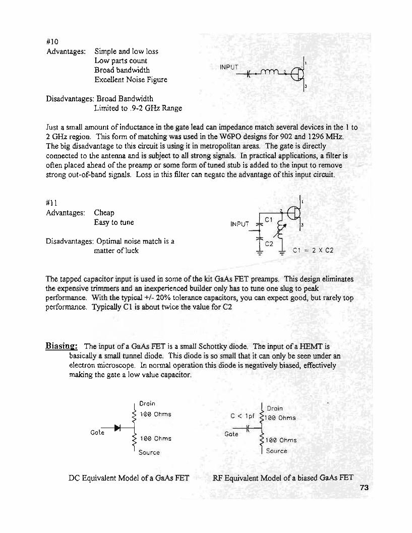
#10Advantages: Simple and low loss
Low parts countBroad bandwidthExcellent Noise Figure
INPUT-If-JTTTL -4-I
Disadvantages: Broad BandwidthLimited to .9-2 GHzRange
Just a small amount of inductance in the gate lead can impedance match several devices in the 1 to2 GHz region. This fonn of matching was used in the W6PO designs for 902 and 1296 MHz.The big disadvantage to this circuit is using it in metropolitan areas. The gate is directlyconnected to the antenna and is subject to all strong signals. In practical applications, a filter isoften placed ahead of the preamp or some fonn of tuned stub is added to the input to removestrong out-of-band signals. Loss in this filter can negate theadvantage of this input circuit.
Disadvantages: Optimal noise match is amatter of luck
#11Advantages: Cheap
Easy to tune
~ Cl: 2 x C2
The tapped capacitor input is used in some ofthe kit GaAs FET preamps. This designeliminatesthe expensive trimmers and an inexperienced builder only has to tune one slug to peakperformance. With the typical +/~ 20%tolerance capacitors, you canexpectgood, but rarely topperformance. Typically C1 is about twice the value for C2
Biasing: The input of a GaAs FET is a small Schottky diode. The input of a HEMT isbasically a small tunnel diode. This diode is so small that it can only be seen under anelectron microscope. In normal operation this diode is negatively biased, effectivelymaking the gate a low value capacitor.
DrainDrain
100 Ohms C < 1pf 100 Ohms
Cote Cote100 Ohms 100 Ohms
Source Source
DC Equivalent Model of a GaAs FET RF Equivalent Model of a biased GaAs FET73

There are two common ways to supply the required negative voltage to the gate ofa GaAs FET.
v- v+Advantages: Direct grounding of the source
Excellent control of all DC parameters
Disadvantages: The negative supply must tum onfirst and tum off last.
Complex power supplies
This method requires power supplies more complex than the preamp.preferred method of getting the most out of a design.
Advantages: Only one positive supply neededThermal run-away virtually eliminated
Disadvantages: The source must be heavily RF by-passed
,
But direct bias is the
.3 Volts
.7 Volt s
Effective Bios on the Gate-.7 Volts
The self-bias circuit was a popular way of making a tube "think"its grid was negatively biased. The voltage drop across the source resistor raises the substrate ofthe device above DC ground. Now grounding the gate gives it a reverse bias. The device alsooperates in a current limiting mode, more current gives a greater negative bias to the gate, turningoff the device. The challenge comes in making the RF part of your circuit think the source isreally grounded and the gate really isn't. Low inductance leadless ceramics, or chip capacitors areused to RF bypass the source. RF Bypassing becomes increasingly difficult at microwavefrequenci es .
Dual Gate Devices:The second gate on a dual gate GaAs FET is normally used for AGe/Gain control of the preampstage. With Japanese devices such as the 3SK971l21/124, NE411 , NE251 , and MGFI IOO, gate 2is nonnalIy run at half the drain voltage. American devices such as Tf' s S3030 and Motorola'sMRF 966 operate gate 2 at 1/4th to Il3rd the drain voltage. Except for biasing of the secondgate, all other circuits in this paper are applicable to both single and dual gate GaAs FErs.

Source Inductance:
Advantages: Improved input matchingLower Noise FigureImproved stability
Disadvantages: Reduced stability
,
There has been quite a bit of work by Chip Angle N6CA and AI Ward WB5LUA using thefeedback from small amountsof source inductance to improve stability and input matching.This Source Inductance can be a small coil, but usually the leads ofthe GaAs FET itself are leftunusually long. Normally source inductance reduces stability and should be avoided. But ifsomeone has gone through the effort to find the optimal source inductance for a device at afrequency, USE IT!
Output Circuits: The output circuit matches the output impedance of the GaAs FET to thenext stage or 50 Ohms. The output circuit also separatesthe RF from the powersupply.
Theoutput match affects Noise Figure, Gain. and circuit stability. There is no one best outputcircuit for alI devices at all frequencies under all conditions, but here are 9 common outputcircuits.
v+#1Advantages: Simple
High stabilityLow pans count
Disadvantages: Low circuit gainUsually no device matching
,Output
Just a dropping resistor and a capacitor is about as simple as you canget. Be sure the resistor is anon-inductive typeand that you have RF bypassing on theopposite side of the resistor. Typicallythis circuit will bave 6 to 8 dB less Galn and a few tenths of a dB higherNoise Figure tban amatched output at VHF frequencies.
#2Advantages: Simple
Low parts count
Disadvantage: No device matchingStability problems
,
v+
Output
While simple and higher stage gain tban a resistor, the RFC and the Capacitor tend to form aresonate circuit at some frequency. Normally this is not a recommended circuit.
75

#3Advantages: Broad frequencyresponse
No tuningSelfshielding
Disadvantages: Broad frequency responsePoor matchingLower gain and higher N.F.
,
V+
The 4 to 1 transformer has been used since the first W6PO designs and the selfshielding of atoroidal transformer simplifies layouts. Modern GaAs FET's tend to have an output impedance ofabout 1000 ohmsat VHFfrequencies. So the 4 to I transformer is ideal onlyfor a 200 to 50 ohmmatch. Motorola improves this by suggesting 9 to I transformers for the MRF966. Also at upperVHF and lowerUHF frequencies, thetransformer tends to look more like an inductor than atransformer. Care must be taken in Ferrite selectionfor the core . Optimal Gain and Noise Figurematching can be difficult to obtain.
#4Advantages: Excellent Matching
Disadvantages: Needs a lot of "Real Estate"below 1 GHz
Coupling problems with the input,
l..-.,+- Output
Normally the Pi output is limited to 1296 and 2304 MHz. The trimmer closest to the deviceusually tunes at min. capacitance and can often be eliminated. White this circuit has been usedaslow as 144 MHz, care must betaken to prevent coupling between the input and output circuits atlow frequencies.
#5Advantages: Extremely versatile
Capable ofmatchingmost any impedance
Disadvantages: Very large assembly below 1 GHzDifficult to build with hand tools
r=~~=~~=-Oou tPut
,
Againthe doublestub tuner is unquestionablythe best method ofproviding an impedance match.While rarely used by hams due to sizeand construction problems. this is the normal method ofcharacterizing GaAs FET's at the factory.
76
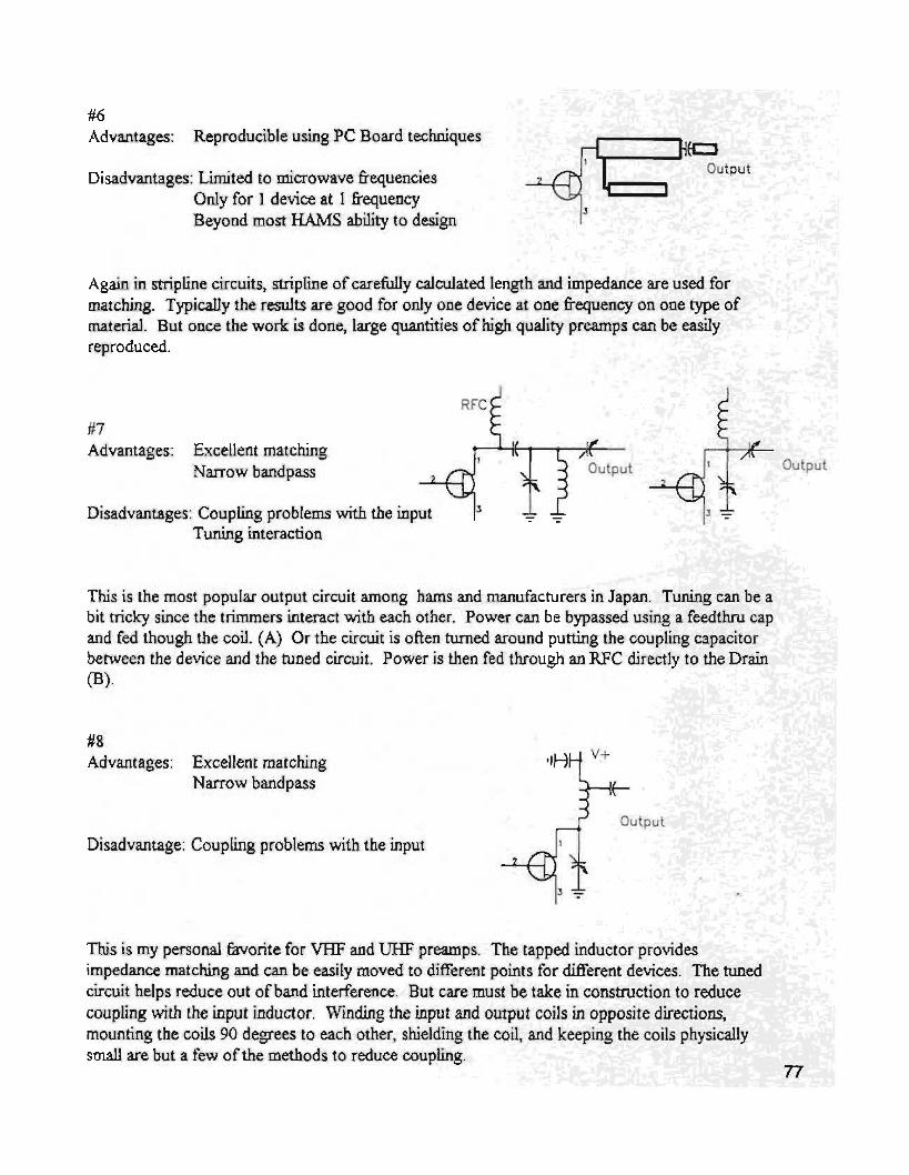
#6Advantages: Reproducible using PC Board techniques
Disadvantages: Limited to microwave frequenciesOnlyfor 1 device at 1 frequencyBeyond most HAMS ability to design
.r.Ji 1*0'1>~~; Output
Again in stripline circuits, stripline of carefully calculated length and impedance are used formatching. Typically the results are good for onlyone device at one frequency on one type ofmaterial. But once the work is done. largequantities ofhighqualitypreamps can be easilyreproduced.
Disadvantages: Coupling problems with the inputTuning interaction
#7Advantages: Excellent matching
Narrow bandpass
RFC
Output Output
This is the most popular output circuit among hams and manufacturers in Japan. Tuning canbe abittricky since the trimmers interact with each other. Power canbe bypassed using a feedthru capand fed though the coil. (A) Orthe circuit is often turned around putting the coupling capacitorbetween thedevice and thetuned circuit. Power is then fed through an RFC directly to theDrain(B).
#8Advantages: Excellent matching
Narrow bandpass
Output
Disadvantage: Coupling problems with the input
This is my personal favorite for VHF and UHF preamps. Thetapped inductor providesimpedance matching and can beeasily moved to different points fordifferent devices. Thetunedcircuit helps reduce out of band interference. But care must be take in construction to reducecoupling with the input inductor. Winding the input and output coils in opposite directions,mountingthe coils90 degrees to each other. shielding the coil. and keeping the coils physicallysmall are but a few of themethods to reduce coupling.
77

Line
~:K
src~ Output
0 Diameter• : HeightImpedance of the output line:
Zo - 138 Log 10 ( Height /Diameter )
#9Advantages: Simple
Disadvantages: Can take up a lot of roomReally onlyuseful on 902,1296, and 2304MHz
This circuit is the dead-bug equivalent of a Stripline circuit. The impedance ofthe wire parallel toan infinite plate can be calculated. Thus witha known impedance and electrical length, animpedance transformation can be accomplished. So just a few inches ofwire about 1/4' abovethe ground plane becomes a tuned circuit. The RFC has quite a bit of stray capacitance to groundand can be attached at different pointalongthe line to improve matching. With Dual Gate devicessuch as the NE4111251 , the RFC should be attached near the GaAs FEr. For Single GateGaAs FEr's like the ATF10135 or MGF 1302, the RFC should be attached at the end ofthe lineMy thanks to Norm WA8EUU for showing me this circuit.
Power supplvNoltage RegulationMost GaAs FEr's like 3 to 5 volts DC at 10 to 20 milliamps. It's nice to have this supply stable,free of spikes and current limiting. In the typical station. reducing spikes is more important thanvoltage regulation. GaAs FETs will oftentolerate 25 to 500;'0 changes involtage with littlevariations in Noise Figureor Gain. but voltage spikes from relay coils and nearby lighting strikescan quickly destroy the device.
Three Termi nal Regulator:
Advantages: Simple and CompactGood Voltage Regulation
Disadvantages: Failure mode puts fullvoltage on the GaAs FErCan passvoltage spikes
l N9 14
+ 12V
7805
Resistor and Zener:
Advantages: Absorbs high intensity spikesFailure modes shorts the supplyto ground protecting the GaAs FErCommon ComponentsReverse PolarityProtection
l N914 2 Wa tt
+1 2V 20a Ohms To GoAs
I IFET
~ -e ~
Disadvantages: Consumes more powerNeeds more space
78

Construction and Operating Tips:
Always leave the Pre-amp Powered Up!Many believe theyare protectingthe GaAs FET by turning it offwbile transmitting. WRONGIWhen operating, the gate of the GaAs FET is negatively biasedabout .5-.7 volts. The FET is damagedwhen the Gate: has a positive voltage and conducts current. So you need enough RF to overcome thenegative bias before it can be hanned. Typically it takes 4 times as much RF leakage to damagea poweruppedGaAs FETthan a turnedoffGaAs FET.
Short Leads. It doesn't take a very long piece of wireto becomean antenna at 10GHz and radiate RF(And Trouble) all around your preamp.
Coils: Wind the input and output coils in the oppositesense, i.e. one right handed and the other lefthanded. This will greatly reduce mutualooupling. Mountthe ooils 90 degree to each other. This will alsogreatly reduce mutualcoupling. Keep the ooils small. A small ooil bas a more localized field and lesscoupling to other circuits.
Ferrite Beads: Ferrite beads behaveas bo<h and RF Absorber and a Low QRF Choke. Theabsorption increases with frequency, so a carefully placed Ferrite Bead can be used to absorb microwaveparasitics while passing 144 MHz signals. At 432 MHz I have used baIfofa bead (cut lengthwise andglued on) with success. See a typical Impedance profile of a Ferrite Bead in the appendix.
Connectors: Type N or SMA connectors should be your first choice for the inputconnector. BNC'syour second choice. Leave the 50239'5 on your HF rig. The output connector is not really critical to thesystem Noise Figure.
Construction: Put the GaAs FET in last as you construe! your preamp. Use a Grounded or cordlesssoldering iron if possible. Ifyou have a regular 2 wiresoldering iron. let it get bot thenunplug it whileactuallysoldering in the GaAs FET. You really don't want 120 VACcapacitivelycoupled from the beatingelement to your expensive and delicate FET. When handing the GaAs FET, always pick it up by theSource or Drain leads. neverthe morestatic sensitive Gate lead.
Static Cha rge DissipatingIf your antenna system is not a direct DC short, put a10K to lOOK static bleeder resistor from the inputconnector to ground. This keeps a static charge frombuilding up on the antenna. arcing acrossthe trimmer cap and zapping the FET.
To InputConnector
100pf
~, /.01uF
Front View Top View
79
•To Output
* Connector•Trimmer CapsAT VHF and UHF, the high impedance point arethe inputs and outputs of the GaAs FET.Just touching these pointswith your tuning toolcan change the tuning.Mount the trimmers so that the rotors are toground, or to the connectors.
Bypass Caps:With self-biased preamps. the source is RF bypassed toground with 100 pfto .l uF capacitors. Most capacitorshave a frequency where they look like a tuned circuit(Self Resonate) . Ifyou are concerned about self resonance,you can bypass the bypass caps.lbat is. put a small value cap across a large value cap.

Absorber: Works 2:reat! Till you put it in the box!Two factors are workingagainst you"ten you put your pre-amp in the box.
First, the boxtries to become a cavity at somefrequency and you've ended up buildinga cavity oseillator.Second. the box is about the same size as microwave waveguide. Let's see, 10GHz waveguide has about 3dBllOO ft of loss, so bowmueb loss is there in your 3 ineb box?
The box itselfbecomes a nearly lossless transmission line.
SI=< Ferriteabsorber really breaks up this feedback path. Usually a 112" by 112" pieceglued to thebottomofthe boxis all you need. Theblackccoductive foam ICs are often packedin worksa1most as,,~1. About a I" by I" or largerpiececan be glued in the bottom of the box. The Foam bas a habit ofcrumblingwith time. I usually put a layerof Clear Spray paint or RlV 0= the foam to bold it together.
Reverse Polarity Protectio n: Always put a diode in series with your preamp. Most anydiode willwork, a IN914 or a IN4148, or even something from the IN400X family. The diodeprotects the preampfrom the reverse polarity spikes from relays, and protects it from you during those little wiring accidentsthat happen during DXpeditions and latenightQSO's
Output Attenuators:The input of a radio is tuned to see 50 Obms, but the radio itselfdoes not look likea 50 Ohm load. So most radios bave a highSWR 00 the input The RF energycan reflect back to the preampand start an oscillation. Usually about 3 dB ofattenuation isenough to stop this osci1latioo.Several feetofRG58 or RGI74 is especially goodas an artenuator.The coax has fur more than 3 dB ofloss at the microwavefrequencies ....'ere the oscillation often occurs.
Tuned tothe normaloperating freq.of the pre - amp
51 Ohms
,
Resistive Sta bilization:This isa cornrnon circuit added to the output sectionof many European Preamps. Theparallel tunedcircuit bas a very highimpedance 00 the operatingfrequency of the pre-amp. So at 144MHz 00 a144 t&iz preamp the circuit has Il:lI OK + 51 Ohmsof resistive loading. This effectively takes the51 Ohm resistor outof the circuit.At frequencies other than 144 MHz, the series tunedcircuit looks like a shortcircuit and the 51 Ohm resistoris across the output.Now,from DC to GHz, (Except at 144MHz) the preamp is operating into a 51 Ohm load.In microwave stripline circuits the 5 I Ohm resistor is often included in the bias voltage and drainpowersupplies to give the preamp a 51 Ohm loadat low frequencies .
Component Layout:Where a component is mounted" is almost as important as the quality of that compooent.While too broad a subject fordiscussionhere, I suggest looking at theGaAs FEr preampspublished in the 1984-1994 ARRL Handbooks. Photos of proven designs are sho.....n.lust follow the general layouts.
80

Tuning Tips:This is the most commonly used input circuit for VHF and UHF preamps. TheQor bandwidth of thiscircuit is highly affected bythe setting for C1. When tuned for best NoiseFigure on 144 Mf-lz, thetypicalvalues for CI is about 6pf and C2 is also about 6 pf But if tuned for lesscoupling, i.e. reduce thevalue ofCl and re-resonate the circuit by increasing the value of C2. the Qof the tuned circuit goes up and theBandwidth decreases.
0dB C1m INPUt
-10 "0e ,
-20 >:;:; C2.'2'"
-e-
-30 '" C1= 1pI-40
100 150 200 MHz
As youcan see, intentional mistuning the inputcangive 20 dB more rejection of FM Broadcast stationsand upper VHF TV stations. This mistuning will cost a balf dBor so of Noise Figure, but this is less lossthan the typical filters . Note: You don't always want to tune forbestNoise Figure orhighest gain.(TNX to W5UNfor making me figure this oocout.)
Ferrite Impedence(F.,4Ufl .., OT Sl-a' 28J
Plot of a typical Ferrite Bead:
iccec
20
•,
, • " 20 so-..., '" '" "..Circuits: OK, lets take all these circu its and combine them like the
choices from a "Blue Plate Special" Menu.81

'"'"Just About as Sim ple as You Can Get
Input #1-Self Bias -Output #1V+
Q 1 Any Sing le Gate GaAs FETFeedthru'IH.0 1uf R
600 Ohms
100 Ohms
12V supply
5V supply
Input
Q1
,
I,.100 pf
Outpu t
C l Ll
L1 ' Em Chip Caps
6 I I 200pf to .01 uF0 _($I - ... ...-
50 MHz
144 MHz222 MHz432 MHz902 MHz
129 6 MHz
2-10pf 10 tu rns 1/ 4" slug tuned
2- 10pf 8 tu rns 3/ 16" dia2- 10 pf 5" "2- 10pf 3 " ".3-3pf Brass Strip 1/ 8" wide
1/8" high 1.5" lang.3- 3pf Brass St rip 1/8" wide
1/ 8"nigh 1.1" lang
All coils 18-22 guagesolid Copper wire
I don't th in k you' ll win any Noise Figure .contests with this . Gain will be a bi t low,but it wil l wor k fin e where limited space is thebiggest prob lem . WA5VJB

IX>...
Conventional DesignInp ut # 2- Self Bias-Out put #8
Zener
FB Ferr ite Bead 3.9-4 .7V 2 Wall 1N9 14
All Coils 3 / 16" dio. '1 +1 2V
Most any Feedthru 'IH200 Ohms
0 1 I Feedthru
single gate GoAs FET .01 uf L2(- .
100 pf Outpu t':' .0 1- . 1uF
FB-C1 0 1Inpu t ,..... r C3
10K <-
*1 hiC2 . L1 . •1 100 Chip Caps WA5VJB- -z: -c- Ohms I I 200pf to .0 1uF
- - -- . .Bon d C1-C2 C3 L1 L2 L2 top turn s
turns turns f rom cold end144 1-1 0pf 4-40pf 9 4 1
All Coils m ode from222 1- 10pf 1-10pf 6 3 1 18-22 guo ge so lid
432 1- 10pf 1- 10pf 4 2 1/ 2 Copper wire.
High 0 Input, High 0 Output and a Power Supply that tokes a lot of abuse.
This design is a proven perf omer in RF poll uted environment s on doz ens of repeaters,
pocket nodes, and EME sta tions . WA5VJB

~
Pi In Pi Out
WASVJB
C. C.
200 Ohm
2 Watt 1N9 14 .
-T T
Chip Caps~ ~I I 200pf to .0 1uF
,
100 pfS.L. C.hip Cap
L I r ~(- 'Outpu t
3.9V
01
100Ohms
•
I ---'l--r--JV\/Ir---1~-,-r-+ 12V01,Feedthru
Feedthru' IH . 1uFI I .01-.1 uF.01 uf RFC
C·
S.L.
C.
T
100pfChip Cap
. , EIInput --1( I II I IF
RFC
01 Any Single Gate GoAs FET
RFC 6 turns 3/ 16' dia
FB = Ferri te Bead
- . -902 MHz
129 6 MHz
23 04 MHz
C.8- l 0pf
.8 - l 0pf
.3- 3pf
S.L.
.2S' wide 1.3'l ong .2' high
.2 S' wide l ' long .2' high
.2S' wide S iong .2' high
St rip Lines
mo de from .020 or ,032'sheet hobby bra ss

Appendix Power OW FET PreampsKent Britain WASVJB
Adapted from OUBUS 95/3
Since the designs for Large Gate FITs were first published in Dec 1990by the VRZA EME Newsletter,the designshave been improved and we have a better understanding of the circuit. My thanks to WB5LUA.who has done extensive computer models and precision measurements of the input circuits.
There is nothing magical to the MGF 1801's. Extremely lownoise preamps have been built with the MGF1601, MGF-211 6, NE0800, and many Avanrek power devices. For the typieal MFG-1302 style GaAs FETthe Iff curves predict device noise figures of .02 to .05 dB in the VHF region. However, Ganuna Opt (BestNoise Figure Muehl typieally rises to over 3000 Ohms. The loadedQ of the input matching has .3 to .4 dB ofloss transfonning the impedance from 50 Ohms to 3000+ Ohms . HEMTs have an even lower noise figure atVHF, but matching to the higherGanuna Opt has even more loss.
By USin8 a GaAs FET with a 800u widegate vs. a 250. widegate, the Ganuna Opt drops to about 900Ohms at VHF. This allows a lower Q,low~r loss, input matching network. The MGF-1801 has a higherdevice Noise Figure than a MGF-1302, but the matcbingnetwork has fur less lossl
For the last 7 years, these designshaveconsistently given .1 to .25 dB Noise Figures at Noise FigureContests.. 1 to . IS dB for the 50 Mf-lz versions, .1 to .25 for the 144 MHz versions, and .2 to .25 dB for the222~ versions has been very consistent. At 432 MHz the Noise Figures rise to .5 to .7 dB and thesedesigns are not competitive.
Fig. #1(Cookbook Input #3) is the mostcommonly used input circuit. The tapped L input consistently gives.1 dB lower Noise Figures than a cavity input. This design has been used by K.B8RQ on 144 MHz EME for 5years with excellent results. Currently, 8 Nonb American EME'ers are using one of these Preamps.
Fig. #2 (Schematic Inser/) is the lowest loss input circuit. but the 3 dB bandwidth is over SOMHz. Thepreamp has gain from 25 MHz to 350 MHzmaking the preamp useless in any urban environment.
Fig. #3 (Cookbook Input # 4)is the cavity input circuit. The cavity is used for both impedance matchingand filtering. This is the circuit [ personally use. My QTH is 10 km from 18 Television transmitters and [trade an extra . ldB of input loss for moreout-of-band rejection.
Fig. N4 (Cookbook Input N.f)is the tapped cavity. The tapped cavity has less loss than the Capacitiveiycoupled cavity, but it can be difficult to find the best tap point. W ith the capacitive coupled cavity, the inputcapacitor can be tuned to a lower capacitance, increasing the cavity Q, trading Noise Figure for a tightbandwidth. This is very useful in high EMI areas sueb as my QTH.
C Bandwaveguide makes an excellent cavity. Theoretically 72 Ohms is the best impodance for the line,but cavities ranging from 30 to 120 Ohms have been built with little difference in Noise Figure.KH6CP has had goodluck using sectionsof In inch Heliax to build up tapped lines for his inputs.
A straight Voltage Regulator is not recommended. Many of these devices are capable of I watt output ifthe preamps oscillates! Current limiting resis tors protect the device: and your receiver. A voltageadjustmentwill help when tuning for that last .1 dB.
A 4 to I transfonner does not match the outputs of these 800u GaAsFETs very well. While a transformerdoes work. a tapped. Low Q tuned circuit works better. The tap point on the output inductor can be moved for
.best match. Besure to wind the input and output coils in oppositedirections.
These designs have been empirically developed during the constru ction of over 40 PowerFet preamps. Wehave not been able to computer model and entire preamp. The GaAs FET manufactures just don't publish the150 MHzNoise Parameterdata for their In watt 10000 MHz devices!
My thanks to Henk Ripe! for first publishing these designs, and to AIWard, WB5LUA for analysis andcleaningup my techni cal points.
85
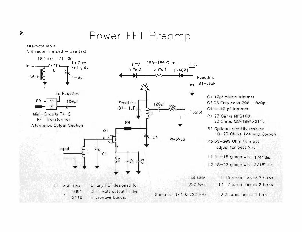
~ Power FET PreampAlternate InputNot recommended - See text
Feedthru
.0 1-. 1uF
150-180 Ohms + 12V
2 Watt lN400 1
'"<r
4.7V1 Watt
1-6pf
LI
10 turns 1/4· die.To GoAsFET gateInput OJ I
.56UH II
Ql
J
FB
L1 14- 16 guog e wire '/4- die.
L2 18-22 quoqe wire 3/ 16- die.
R2 Optional stabi lity resistor10-27 Ohms 1/4 wott Corbon
R3 50 -200 Ohm trim pot
adjust fo r bes t N,r.
Cl 10pf piston trimmer
C2,C3 Chip cops 200-1000pf
C4 4-40 pf trimmer
Rl 27 Ohms MFG1 60 122 Ohms MGF180 1/2116
Output
WA5VJBC4
100pf
~~-' r
rr<r
Feedthru.0 1-. 1uF
C1--'
~
Input
To Feedthru
FB~ 100pf
~~Mini-Circuits T4-2
RF Transfo rmer
Alternative Output Section
Q1 MGF 1601180 1
2116
Or any FET designed for
.2-1 watt output in the
microwave bonds .
144 MHz
222 MHz
Same for 144 & 222 MHz
L1 10 turns tap at .3 turns
L1 7 turns top at 2 turns
L2 3 turns top ot 1 turn

APPENDIX #2
Drain
Gote
1~0 Ohms
100 Ohms
Source
Res ist ive Model
of 0 GoAs FET
Testing GaAs FETS:
10K +Resistor
Analog VOM with a 1.5 Volt Battery
When I first saw WB5LUA make this test, I gasped, but it makes sense.
Use a YOM with a I.5 Volt battery!!No 9 V powered DMM's or 22 Volt Simpsons allowed here.This is a great place for that old $5 Radio Shack YOM.
I.5 volts is less than the break down voltages of the gate, so it won't hurt anything.The 10K resistor limits current to .1 rna, and that's not enough current to hurt the gate.Just zero your meter, put in a 10K resistor on one lead, and add 10K to all the resistancereadings. Some of the older FET's usedthe Slashed gate as the Drain. You can use thistest to make sure you're putting the FET inthe right way_ For an in-circuit test, justunsolder the gate lead, or unground the input coil. Now checkthe gate for lO.5K oneway, and - the other. 99.99%of the time, if the FETs been zapped, the gate is gone.
As always, take precautions against static electricity.
Kent Britain WASVJB
"f?-B'" c :~1'"Typical Readings 10.2K'.Y
87

IhP" f ("",,,,,ee-Iov
a.. ) Cvu ";"",6
LatJac,·/ort.
1'1Gf'- 1'8'C> /
Lav:I'/5fyle
?1 GF- 2//0
l'1"u,,!,J a" eleJ-",'cQ //Y150/" t c) fbI {;,''1 k