full-bridge dmos pwm motor drivers · full-bridge dmos pwm motor drivers a4952 and a4953 allegro...
TRANSCRIPT

DescriptionDesigned for pulse width modulated (PWM) control of DC motors, the A4952 and A4953 are capable of peak output currents to ±2 A and operating voltages to 40 V.
Input terminals are provided for use in controlling the speed and direction of a DC motor with externally applied PWM control signals. Internal synchronous rectification control circuitry is provided to lower power dissipation during PWM operation.
Internal circuit protection includes overcurrent protection, motor lead short to ground or supply, thermal shutdown with hysteresis, undervoltage monitoring of VBB, and crossover-current protection.
The A4952 is provided in a low-profile 10-pin MSOP package (suffix LY) and the A4953 is provided in a low-profile 8-pin SOICN package (suffix LJ). Both packages have an exposed thermal pad, and are lead (Pb) free, with 100% matte tin leadframe plating.
A4952-DS, Rev. 3
Features and Benefits• Low RDS(on) outputs• Overcurrent protection (OCP)MotorshortprotectionMotorleadshorttogroundprotectionMotorleadshorttobatteryprotection
• Low Power Standby mode • Adjustable PWM current limit• Synchronous rectification• Internal undervoltage lockout (UVLO) • Crossover-current protection• Fault output (A4952 only)• Selectable retry (A4952 only)
Full-Bridge DMOS PWM Motor Drivers
Functional Block Diagram
A4952 and A4953
Control Logic
LSS
OUT1
OUT2
VBB
IN1
IN2
Charge PumpOSC
Disable
Load Supply
UVLO
VREF
7V
VINT
A4952 only
GND
÷ (Optional)
TSD
10
RTRY
FLTn
A4952 only
Packages:
Not to scale
8-pin SOICN with exposed thermal pad
(LJ package)
10-pin MSOP with exposed thermal pad
(LY package)
Full-Bridge DMOS PWM Motor DriversA4952 andA4953
2Allegro MicroSystems, LLC115 Northeast CutoffWorcester, Massachusetts 01615-0036 U.S.A.1.508.853.5000; www.allegromicro.com
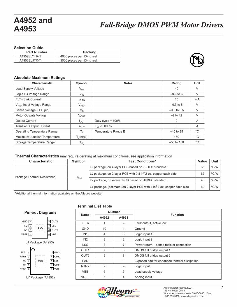
Terminal List Table
NameNumber
FunctionA4952 A4953
FLTn 1 – Fault output, active low
GND 10 1 Ground
IN1 4 3 Logic input 1
IN2 3 2 Logic input 2
LSS 8 7 Power return – sense resistor connection
OUT1 7 6 DMOS full bridge output 1
OUT2 9 8 DMOS full bridge output 2
PAD – – Exposed pad for enhanced thermal dissipation
RTRY 2 – Logic input
VBB 6 5 Load supply voltage
VREF 5 4 Analog input
Pin-out Diagrams
Absolute Maximum RatingsCharacteristic Symbol Notes Rating Unit
Load Supply Voltage VBB 40 V
Logic I/O Voltage Range VIN –0.3 to 6 V
FLTn Sink Current IFLTN 10 mA
VREF Input Voltage Range VREF –0.3 to 6 V
Sense Voltage (LSS pin) VS –0.5 to 0.5 V
Motor Outputs Voltage VOUT –2 to 42 V
Output Current IOUT Duty cycle = 100% 2 A
Transient Output Current iOUT TW < 500 ns 6 A
Operating Temperature Range TA Temperature Range E –40 to 85 °C
Maximum Junction Temperature TJ(max) 150 °C
Storage Temperature Range Tstg –55 to 150 °C
Selection GuidePart Number Packing
A4952ELYTR-T 4000 pieces per 13-in. reelA4953ELJTR-T 3000 pieces per 13-in. reel
Thermal Characteristics may require derating at maximum conditions, see application informationCharacteristic Symbol Test Conditions* Value Unit
Package Thermal Resistance RθJA
LJ package, on 4-layer PCB based on JEDEC standard 35 ºC/W
LJ package, on 2-layer PCB with 0.8 in2. 2-oz. copper each side 62 ºC/W
LY package, on 4-layer PCB based on JEDEC standard 48 ºC/W
LY package, (estimate) on 2-layer PCB with 1 in2. 2-oz. copper each side 60 ºC/W
*Additional thermal information available on the Allegro website.
8
7
6
5
1
2
3
4
OUT2
LSS
OUT1
VBB
GND
IN2
IN1
VREF
PAD
FLTn
RTRY
IN2
IN1
VREF
GND
OUT2
LSS
OUT1
VBB
1
2
3
4
5
10
9
8
7
6
PAD
LJ Package (A4953)
LY Package (A4952)
Full-Bridge DMOS PWM Motor DriversA4952 andA4953
3Allegro MicroSystems, LLC115 Northeast CutoffWorcester, Massachusetts 01615-0036 U.S.A.1.508.853.5000; www.allegromicro.com
ELECTRICAL CHARACTERISTICS Valid at TJ = 25°C, unless otherwise specifiedCharacteristics Symbol Test Conditions Min. Typ. Max. Unit
GeneralLoad Supply Voltage Range VBB 8 – 40 V
RDS(on) Sink + Source Total RDS(on)IOUT = |1.5 A|, TJ = 25°C – 0.8 1.0 Ω
IOUT = |1.5 A|, TJ = 125°C – 1.3 1.6 Ω
Load Supply Current IBBfPWM < 30 kHz – 10 – mA
Low Power Standby mode – – 10 µA
Body Diode Forward Voltage VfSource diode, If = –1.5 A – – 1.5 V
Sink diode, If = 1.5 A – – 1.5 V
Logic I/O Inputs
Logic Input Voltage Range
VIN(1) INx pins 2.0 – – V
VIN(0) INx pins – – 0.8 V
VIN(STANDBY) INx pins, Low Power Standby mode – – 0.4 V
Logic Input Pull-Down Resistance RRRLOGIC(PD) VIN = 0 V = IN1 = IN2 – 50 – kΩ
Logic Input Current IIN(1) INx pins, VIN = 2.0 V – 40 100 µA
IIN(0) INx pins, VIN = 0.8 V – 16 40 µA
Input Hysteresis VHYS – 250 550 mV
Logic I/O Inputs (A4952 only)Retry Input Voltage VRTRY RTRY pin = valid – – 200 mV
Retry Overcurrent Protection Pullup Voltage VRTRY(OC) RTRY pin = open – 3 – V
Retry Short Circuit Current IRTRY RTRY pin = GND – 10 – µA
Fault Output Voltage VRST FLTn pin, IOUT = 1 mA – – 0.5 V
Fault Output Leakage Current ILK FLTn pin, no fault, pull-up to 5 V – – 1 µA
TimingCrossover Delay tCOD 50 400 500 ns
VREF Input Voltage Range VREF 0 – 5 V
Current Gain A V
VREF / ISS , VREF = 5 V 9.5 – 10.5 V/V
VREF / ISS , VREF = 2.5 V 9.0 – 10.0 V/V
VREF / ISS , VREF = 1 V 8.0 – 10.0 V/V
Blank Time tBLANK 2 3 4 µs
Constant Off-time toff 16 25 34 µs
Standby Timer tst IN1 = IN2 < VIN(STANDBY) – 1 1.5 ms
Power-Up Delay tpu – – 30 µs
Protection CircuitsUVLO Enable Threshold VBBUVLO VBB increasing 7 7.5 7.95 V
UVLO Hysteresis VBBUVLOhys – 500 – mV
Thermal Shutdown Temperature TJTSD Temperature increasing – 160 – °C
Thermal Shutdown Hysteresis TTSDhys Recovery = TJTSD – TTSDhys – 20 – °C
Overcurrent Protection Limit IOCP 2.5 – 6.5 A
Overcurrent Protection Pulse Width tOCP 1 – 4 µs
Full-Bridge DMOS PWM Motor DriversA4952 andA4953
4Allegro MicroSystems, LLC115 Northeast CutoffWorcester, Massachusetts 01615-0036 U.S.A.1.508.853.5000; www.allegromicro.com
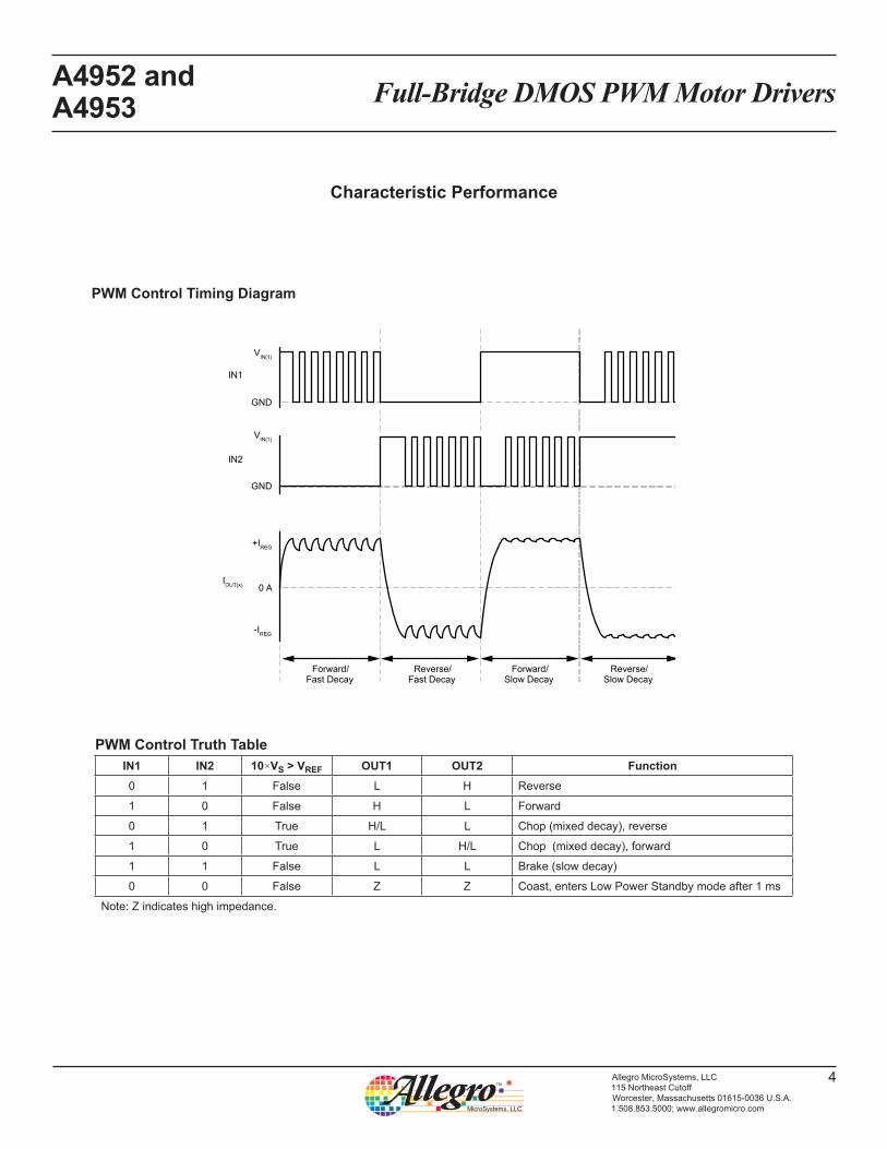
Characteristic Performance
PWM Control Timing Diagram
PWM Control Truth TableIN1 IN2 10×VS > VREF OUT1 OUT2 Function0 1 False L H Reverse
1 0 False H L Forward
0 1 True H/L L Chop (mixed decay), reverse
1 0 True L H/L Chop (mixed decay), forward
1 1 False L L Brake (slow decay)
0 0 False Z Z Coast, enters Low Power Standby mode after 1 ms
Note: Z indicates high impedance.
Reverse/Fast Decay
Reverse/Slow Decay
Forward/Fast Decay
Forward/Slow Decay
GND
GND
+IREG
0 A
-IREG
IN1
IN2
IOUT(x)
VIN(1)
VIN(1)
Full-Bridge DMOS PWM Motor DriversA4952 andA4953
5Allegro MicroSystems, LLC115 Northeast CutoffWorcester, Massachusetts 01615-0036 U.S.A.1.508.853.5000; www.allegromicro.com
Functional Description
Device OperationThe A4952 and A4953 are designed to operate DC motors. The output drivers are all low-RDS(on) , N-channel DMOS drivers that feature internal synchronous rectification to reduce power dissipation. The current in the output full bridge is regulated with fixed off-time pulse width modulated (PWM) control circuitry. The IN1 and IN2 inputs allow two-wire control for the bridge.
Protection circuitry includes internal thermal shutdown, and pro-tection against shorted loads, or against output shorts to ground or supply. Undervoltage lockout prevents damage by keeping the outputs off until the driver has enough voltage to operate nor-mally.
Standby ModeLow Power Standby mode is activated when both input (INx) pins are low for longer than 1 ms. Low Power Standby mode disables most of the internal circuitry, including the charge pump and the regulator. When the A4952/A4953 is coming out of standby mode, the charge pump should be allowed to reach its regulated voltage (a maximum delay of 30 µs) before any PWM commands are issued to the device.
Internal PWM Current ControlInitially, a diagonal pair of source and sink FET outputs are enabled and current flows through the motor winding and the optional external current sense resistor, RS . When the voltage across RS equals the comparator trip value, then the current sense comparator resets the PWM latch. The latch then turns off the sink and source FETs (Mixed Decay mode).
VREFThe maximum value of current limiting is set by the selection of RSx and the voltage at the VREF pin. The transconductance func-tion is approximated by the maximum value of current limiting, ITripMAX (A), which is set by:
ITripMAX = AV RS
VREF
where VREF is the input voltage on the VREF pin (V) and RS is theresistanceofthesenseresistor(Ω)ontheLSSterminal.
Overcurrent ProtectionIn the A4952, a current monitor will protect the IC from damage due to output shorts. The internal Overcurrent Protection (OCP) has the following features:
• Fault Output (FLTn pin). If a short is detected, the open drain FLTn output signal goes low.
• Retry Input (RTRY pin). Sets the action taken by the IC to re-spond to an OCP fault. If the RTRY pin is tied to GND, then the outputs will be turned-on again after a 2-ms timeout, to check if a fault condition remains. If the RTRY pin is left open, then the fault will be latched, and the IC will disable the outputs. The fault latch can only be cleared by coming out of Low Power Standby mode or by cycling the power to VBB.
Note: The A4953 overcurrent protection behaves in the same manner but the fault is latched and can only be reset by putting the device into standby mode or by cycling the power to VBB.
During OCP events, Absolute Maximum Ratings may be exceeded for a short period of time before the device latches.
ShutdownIf the die temperature increases to approximately 160°C, the full bridge outputs will be disabled until the internal temperature falls below a hysteresis, TTSDhys , of 20°C. Internal UVLO is present on VBB to prevent the output drivers from turning-on below the UVLO threshold.
BrakingThe braking function is implemented by driving the device in Slow Decay mode, which is done by applying a logic high to both inputs, after a bridge-enable Chop command (see PWM Control Truth Table). Because it is possible to drive current in both direc-tions through the DMOS switches, this configuration effectively shorts-out the motor-generated BEMF, as long as the Chop com-mand is asserted. The maximum current can be approximated by VBEMF / RL . Care should be taken to ensure that the maximum ratings of the device are not exceeded in worse case braking situ-ations: high speed and high-inertia loads.
Full-Bridge DMOS PWM Motor DriversA4952 andA4953
6Allegro MicroSystems, LLC115 Northeast CutoffWorcester, Massachusetts 01615-0036 U.S.A.1.508.853.5000; www.allegromicro.com
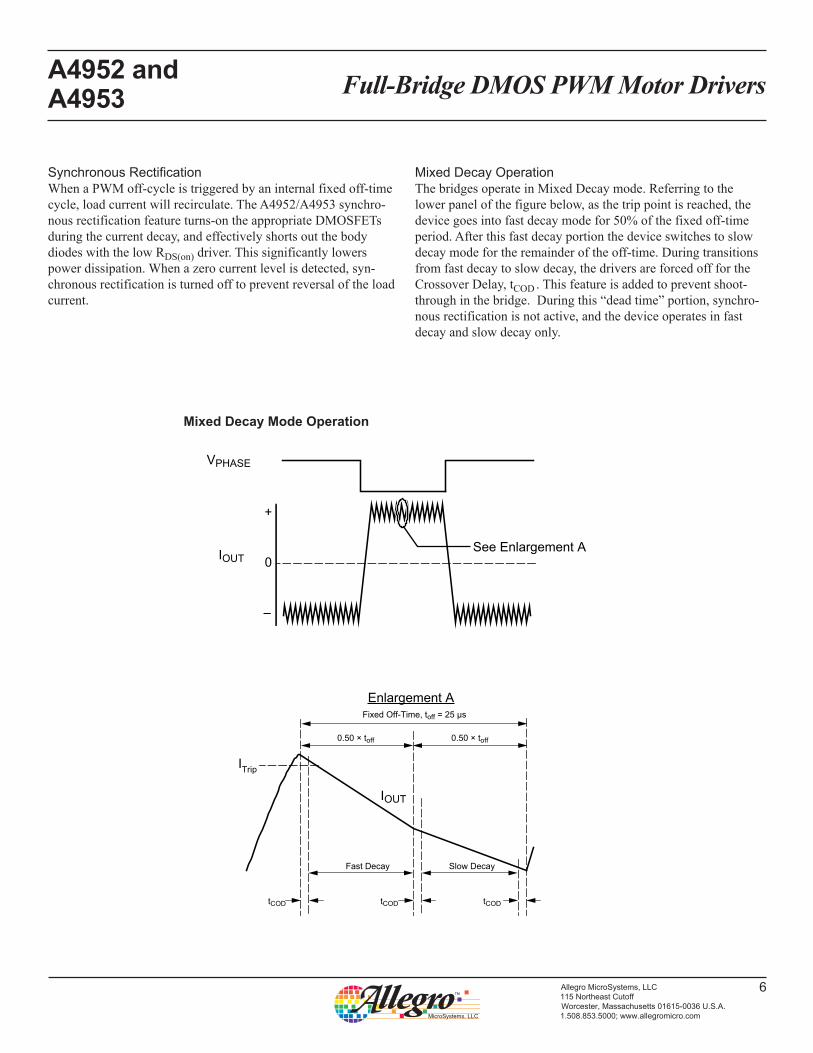
Synchronous Rectification When a PWM off-cycle is triggered by an internal fixed off-time cycle, load current will recirculate. The A4952/A4953 synchro-nous rectification feature turns-on the appropriate DMOSFETs during the current decay, and effectively shorts out the body diodes with the low RDS(on) driver. This significantly lowers power dissipation. When a zero current level is detected, syn-chronous rectification is turned off to prevent reversal of the load current.
Mixed Decay Operation The bridges operate in Mixed Decay mode. Referring to the lower panel of the figure below, as the trip point is reached, the device goes into fast decay mode for 50% of the fixed off-time period. After this fast decay portion the device switches to slow decay mode for the remainder of the off-time. During transitions from fast decay to slow decay, the drivers are forced off for the Crossover Delay, tCOD . This feature is added to prevent shoot-through in the bridge. During this “dead time” portion, synchro-nous rectification is not active, and the device operates in fast decay and slow decay only.
Mixed Decay Mode Operation
VPHASE
IOUT
IOUT
+
–
0See Enlargement A
Enlargement A
tCODtCODtCOD
Fixed Off-Time, toff = 25 µs
Fast Decay Slow Decay
ITrip
0.50 × toff 0.50 × toff
Full-Bridge DMOS PWM Motor DriversA4952 andA4953
7Allegro MicroSystems, LLC115 Northeast CutoffWorcester, Massachusetts 01615-0036 U.S.A.1.508.853.5000; www.allegromicro.com
Application Information
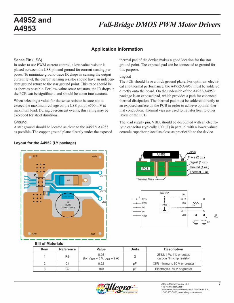
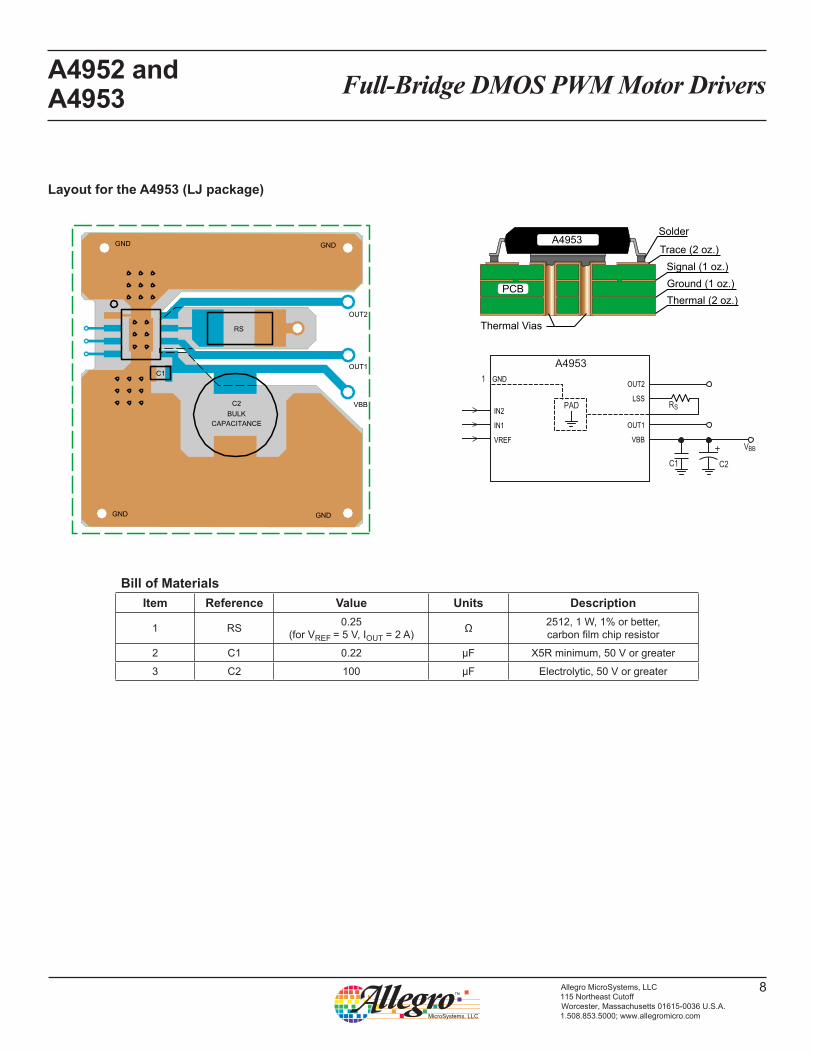
Sense Pin (LSS)In order to use PWM current control, a low-value resistor is placed between the LSS pin and ground for current sensing pur-poses. To minimize ground-trace IR drops in sensing the output current level, the current sensing resistor should have an indepen-dent ground return to the star ground point. This trace should be as short as possible. For low-value sense resistors, the IR drops in the PCB can be significant, and should be taken into account.
When selecting a value for the sense resistor be sure not to exceed the maximum voltage on the LSS pin of ±500 mV at maximum load. During overcurrent events, this rating may be exceeded for short durations.
GroundA star ground should be located as close to the A4952/ A4953 as possible. The copper ground plane directly under the exposed
thermal pad of the device makes a good location for the star ground point. The exposed pad can be connected to ground for this purpose.
LayoutThe PCB should have a thick ground plane. For optimum electri-cal and thermal performance, the A4952/A4953 must be soldered directly onto the board. On the underside of the A4952/A4953 package is an exposed pad, which provides a path for enhanced thermal dissipation. The thermal pad must be soldered directly to an exposed surface on the PCB in order to achieve optimal ther-mal conduction. Thermal vias are used to transfer heat to other layers of the PCB.
The load supply pin, VBB, should be decoupled with an electro-lyticcapacitor(typically100μF)inparallelwithalowervaluedceramic capacitor placed as close as practicable to the device.
GND
RS
GND
GND GND
C1
BULKCAPACITANCE
VBB
OUT2
OUT1
C2
VBB
1
PAD
A4952
C1 C2
OUT2
LSS
OUT1
VBB
FLTn
RTRY
IN2
IN1
VREF
GND
RS
PCB
Thermal Vias
LYPackage
Trace (2 oz.)Signal (1 oz.)Ground (1 oz.)Thermal (2 oz.)
SolderA4952
Bill of MaterialsItem Reference Value Units Description
1 RS 0.25 (for VREF = 5 V, IOUT = 2 A) Ω 2512, 1 W, 1% or better,
carbon film chip resistor
2 C1 0.22 µF X5R minimum, 50 V or greater
3 C2 100 µF Electrolytic, 50 V or greater
Layout for the A4952 (LY package)
Full-Bridge DMOS PWM Motor DriversA4952 andA4953
8Allegro MicroSystems, LLC115 Northeast CutoffWorcester, Massachusetts 01615-0036 U.S.A.1.508.853.5000; www.allegromicro.com
GND
RS
GND
GND GND
C1
BULKCAPACITANCE
VBB
OUT2
OUT1
C2
VBB
1
PAD
A4953
C1 C2
OUT2
LSS
OUT1
VBB
IN2
IN1
VREF
GND
RS
PCB
Thermal Vias
Trace (2 oz.)Signal (1 oz.)Ground (1 oz.)Thermal (2 oz.)
SolderA4953
Bill of MaterialsItem Reference Value Units Description
1 RS 0.25 (for VREF = 5 V, IOUT = 2 A) Ω 2512, 1 W, 1% or better,
carbon film chip resistor
2 C1 0.22 µF X5R minimum, 50 V or greater
3 C2 100 µF Electrolytic, 50 V or greater
Layout for the A4953 (LJ package)

Full-Bridge DMOS PWM Motor DriversA4952 andA4953
9Allegro MicroSystems, LLC115 Northeast CutoffWorcester, Massachusetts 01615-0036 U.S.A.1.508.853.5000; www.allegromicro.com
Package LJ, 8-Pin SOICNwith exposed thermal pad
3.30
21
8
Reference land pattern layout (reference IPC7351 SOIC127P600X175-9AM); all pads a minimum of 0.20 mm from all adjacent pads; adjust as necessary to meet application process requirements and PCB layout tolerances; when mounting on a multilayer PCB, thermal vias at the exposed thermal pad land can improve thermal dissipation (reference EIA/JEDEC Standard JESD51-5)
PCB Layout Reference ViewC
1.27
5.602.41
1.75
0.65
2.41 NOM
3.30 NOM
CSEATINGPLANE
1.27 BSC
GAUGE PLANESEATING PLANE
A Terminal #1 mark area
B
C
B
21
8
CSEATINGPLANEC0.10
8X
0.25 BSC
1.04 REF
1.70 MAX
For Reference Only; not for tooling use (reference MS-012BA)Dimensions in millimetersDimensions exclusive of mold flash, gate burrs, and dambar protrusions Exact case and lead configuration at supplier discretion within limits shown
4.90 ±0.10
3.90 ±0.10 6.00 ±0.20
0.510.31 0.15
0.00
0.250.17
1.270.40
8°0°
Exposed thermal pad (bottom surface); dimensions may vary with device
A
Branded Face
Full-Bridge DMOS PWM Motor DriversA4952 andA4953
10Allegro MicroSystems, LLC115 Northeast CutoffWorcester, Massachusetts 01615-0036 U.S.A.1.508.853.5000; www.allegromicro.com
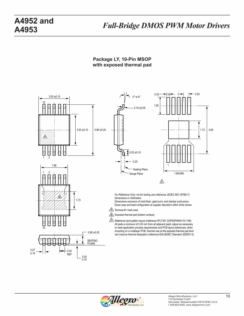
Package LY, 10-Pin MSOPwith exposed thermal pad
Terminal #1 mark area
A
Gauge PlaneSeating Plane
0.86 ±0.05
SEATINGPLANE
0.50REF
0.2521
10
21
10
A
B
C
C
0.53 ±0.10
0.15 ±0.05
0.050.15
0° to 6°3.00 ±0.10
3.00 ±0.10 4.88 ±0.20 1.73 4.60
1.98
1.98 MIN
1.73
21
10
1
0.30 0.50
1.65
0.270.18
For Reference Only; not for tooling use (reference JEDEC MO-187BA-T)Dimensions in millimetersDimensions exclusive of mold flash, gate burrs, and dambar protrusions Exact case and lead configuration at supplier discretion within limits shown
B
Exposed thermal pad (bottom surface)
Reference land pattern layout (reference IPC7351 SOP50P490X110-11M)All pads a minimum of 0.20 mm from all adjacent pads; adjust as necessary to meet application process requirements and PCB layout tolerances; when mounting on a multilayer PCB, thermal vias at the exposed thermal pad land can improve thermal dissipation (reference EIA/JEDEC Standard JESD51-5)

Full-Bridge DMOS PWM Motor DriversA4952 andA4953
11Allegro MicroSystems, LLC115 Northeast CutoffWorcester, Massachusetts 01615-0036 U.S.A.1.508.853.5000; www.allegromicro.com
Copyright ©2010-2014, Allegro MicroSystems, LLCAllegro MicroSystems, LLC reserves the right to make, from time to time, such departures from the detail specifications as may be required to
permit improvements in the performance, reliability, or manufacturability of its products. Before placing an order, the user is cautioned to verify that the information being relied upon is current.
Allegro’s products are not to be used in any devices or systems, including but not limited to life support devices or systems, in which a failure of Allegro’s product can reasonably be expected to cause bodily harm.
The information included herein is believed to be accurate and reliable. However, Allegro MicroSystems, LLC assumes no responsibility for its use; nor for any infringement of patents or other rights of third parties which may result from its use.
Revision HistoryRevision Revision Date Description of Revision
Rev. 3 March 12, 2014 Update Electrical Characteristics table