ft311d and ft312d demo apk user guide - · pdf filean_208 ft311d and ft312d...
TRANSCRIPT
Use of FTDI devices in life support and/or safety applications is entirely at the user’s risk, and the user agrees to defend, indemnify and hold FTDI harmless from any and all damages, claims, suits
or expense resulting from such use.
Future Technology Devices International Limited (FTDI) Unit 1, 2 Seaward Place, Glasgow G41 1HH, United Kingdom Tel.: +44 (0) 141 429 2777 Fax: + 44 (0) 141 429 2758
Web Site: http://ftdichip.com Copyright © 2013 Future Technology Devices International Limited
Application Note
AN_208
FT311D and FT312D Demo_APK_User_GuideFT311D and
FT312D Demo_APK_User_Guide
Version1.3
Issue Date: 2013-09-09
FTDI’s FT311D device is targeted specifically at providing a data bridge from an Android USB device port to alternative interfaces such as GPIO, UART, PWM, I2C or SPI, while the FT312D device is specific to UART interfaces. To use the device requires JAVA applications developed to run on Android
platforms that support Open Accessory Mode (3.1 onwards). This user guide describes how to use the sample applications FTDI has provided.
Application Note
AN_208 FT311D and FT312D Demo_APK_User_Guide Version 1.3
Document Reference No.: FT_000666 Clearance No.: FTDI# 306
1
Copyright © 2013 Future Technology Devices International Limited
Table of Contents
1 Introduction .................................................................................................................................... 3
1.1 Overview ................................................................................................................................ 3
2 Loading Examples onto the Android ............................................................................................... 4
3 Examples ......................................................................................................................................... 5
3.1 Avoid Android read() Pitfall ................................................................................................... 5
3.2 UART Loopback ...................................................................................................................... 5
3.2.1 UART Loopback Hardware ................................................................................................ 5
3.2.2 UART Loopback Application .............................................................................................. 6
3.2.3 Menu Functions................................................................................................................. 8
3.2.4 Multi-Applications ........................................................................................................... 10
3.2.5 Auto-run or Manually-run ............................................................................................... 10
3.2.6 Running UART Loopback Multiple Times ........................................................................ 10
3.3 UART Test ............................................................................................................................ 12
3.3.1 Hardware Setup for UART Test Application .................................................................... 12
3.3.2 UART Test Application ..................................................................................................... 12
3.4 GPIO Demo .......................................................................................................................... 14
3.4.1 GPIO Test Hardware ........................................................................................................ 14
3.4.2 GPIO Application ............................................................................................................. 14
3.5 PWM Demo ......................................................................................................................... 16
3.5.1 PWM Test Hardware ....................................................................................................... 16
3.5.2 PWM Application ............................................................................................................ 16
3.6 I2C Demo .............................................................................................................................. 18
3.6.1 I2C Test Hardware ............................................................................................................ 18
3.6.2 I2C Application ................................................................................................................. 18
3.7 SPI Slave Demo .................................................................................................................... 20
3.7.1 SPI Slave Test Hardware .................................................................................................. 20
3.7.2 SPI Slave Application ....................................................................................................... 20
3.8 SPI Master Demo ................................................................................................................. 22
3.8.1 SPI Master Test Hardware ............................................................................................... 22
Application Note
AN_208 FT311D and FT312D Demo_APK_User_Guide Version 1.3
Document Reference No.: FT_000666 Clearance No.: FTDI# 306
2
Copyright © 2013 Future Technology Devices International Limited
3.8.2 SPI Master Application .................................................................................................... 22
4 Contact Information ...................................................................................................................... 24
Appendix A – References ...................................................................................................................... 25
Document References ....................................................................................................................... 25
Acronyms and Abbreviations ............................................................................................................ 25
Appendix B – List of Figures .................................................................................................................. 26
Appendix C– Revision History ............................................................................................................... 27
Application Note
AN_208 FT311D and FT312D Demo_APK_User_Guide Version 1.3
Document Reference No.: FT_000666 Clearance No.: FTDI# 306
3
Copyright © 2013 Future Technology Devices International Limited
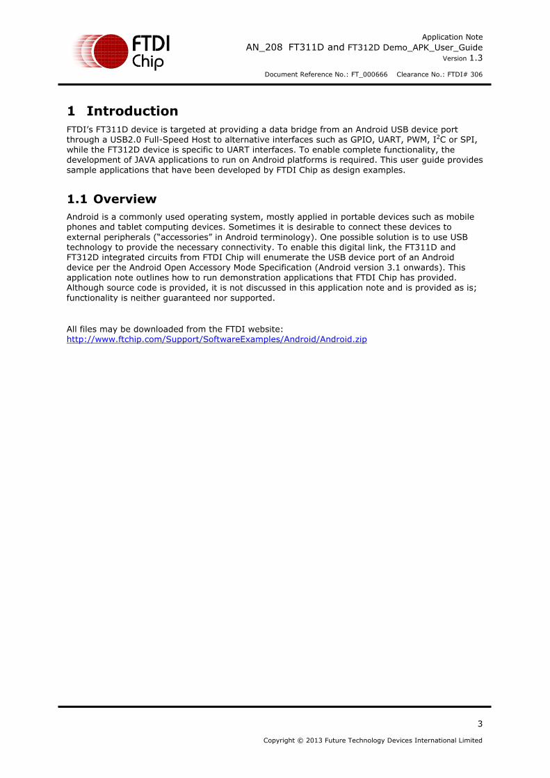
1 Introduction
FTDI’s FT311D device is targeted at providing a data bridge from an Android USB device port through a USB2.0 Full-Speed Host to alternative interfaces such as GPIO, UART, PWM, I2C or SPI, while the FT312D device is specific to UART interfaces. To enable complete functionality, the development of JAVA applications to run on Android platforms is required. This user guide provides
sample applications that have been developed by FTDI Chip as design examples.
1.1 Overview
Android is a commonly used operating system, mostly applied in portable devices such as mobile phones and tablet computing devices. Sometimes it is desirable to connect these devices to
external peripherals (“accessories” in Android terminology). One possible solution is to use USB technology to provide the necessary connectivity. To enable this digital link, the FT311D and FT312D integrated circuits from FTDI Chip will enumerate the USB device port of an Android
device per the Android Open Accessory Mode Specification (Android version 3.1 onwards). This application note outlines how to run demonstration applications that FTDI Chip has provided. Although source code is provided, it is not discussed in this application note and is provided as is;
functionality is neither guaranteed nor supported.
All files may be downloaded from the FTDI website: http://www.ftchip.com/Support/SoftwareExamples/Android/Android.zip
Application Note
AN_208 FT311D and FT312D Demo_APK_User_Guide Version 1.3
Document Reference No.: FT_000666 Clearance No.: FTDI# 306
4
Copyright © 2013 Future Technology Devices International Limited
2 Loading Examples onto the Android
An “executable” file for Android has the extension, .apk. To load the file onto the Android operating system it is recommended to follow the steps below.
Step 1 is to allow non-market applications to install. This is done from the settings window. Select
security -> unknown sources, to allow the application to install.
Step 2 is to copy the .apk file to the Android device. This can be done by connecting the device directly to your desktop/laptop and simply copying the file to the desired destination with Windows Explorer (assumes a windows PC). An Android app such as “File Expert” may then be used to browse to the file on the Android device.
Step 3 is to open the apk file which should launch the application installer to allow the application to be installed. By default the application will appear in the applications window of your device. Note, dragging it to the desktop is optional but not essential.
For advanced users, if the PC side USB driver for the Android device is properly installed, with the help of the Android SDK, the application may be installed using the adb (Android Debug Bridge) to install applications from the PC. The steps are:
Step 1 is to connect the Android device with the PC via the USB cable. Please make sure only one Android device is connected to the PC at a time. Next, open a command prompt window and issue the “adb devices” command to check if the requirement is met:
adb devices╝
List of devices attached 4df1f70914328f09 device
When a device is successfully found by the Android SDK, it will display its ID and device state
below the “List of devices attached” line. Note: ensure there is only one device attached to PC.
Step 2 is to use a command prompt window, changing the directory to where the .apk files are stored, and using “adb install <your_android_app>.apk” command to install. Note, please replace “<your_android_app>.apk” with the real file name.
Application Note
AN_208 FT311D and FT312D Demo_APK_User_Guide Version 1.3
Document Reference No.: FT_000666 Clearance No.: FTDI# 306
5
Copyright © 2013 Future Technology Devices International Limited
3 Examples
Examples exist to verify each interface:
UARTLoopback.apk for FT311D or FT312D UARTTest.apk for FT311D or FT312D GPIODemo.apk for FT311D
PWMDemo.apk for FT311D I2CDemo.apk for FT311D SPIMasterDemo.apk for FT311D SPISlaveDemo.apk for FT311D
3.1 Avoid Android read() Pitfall
In certain cases, the accessory has to support plug-in for a relatively long time and the user might
manually re-run the application multiple times while the accessory is attached. When creating applications for this scenario, one could easily encounter an Android framework limitation caused by the FileInputStream.read() block-reading behaviour.
The issue occurs when an application comes to an end due to the user putting it to the background or running another application. The read thread holding the FileInputStream does not clean up and exit, because the FileInputStream.read() is still in block-reading, and not able to return as expected. One way to overcome this limitation is to send an END request defined by users and have the connected UART device respond with an OK signal to let the read() return.
Please refer to UART Loopback demo application source for a sample design.
3.2 UART Loopback
This UART example application is named UARTLookback.apk.
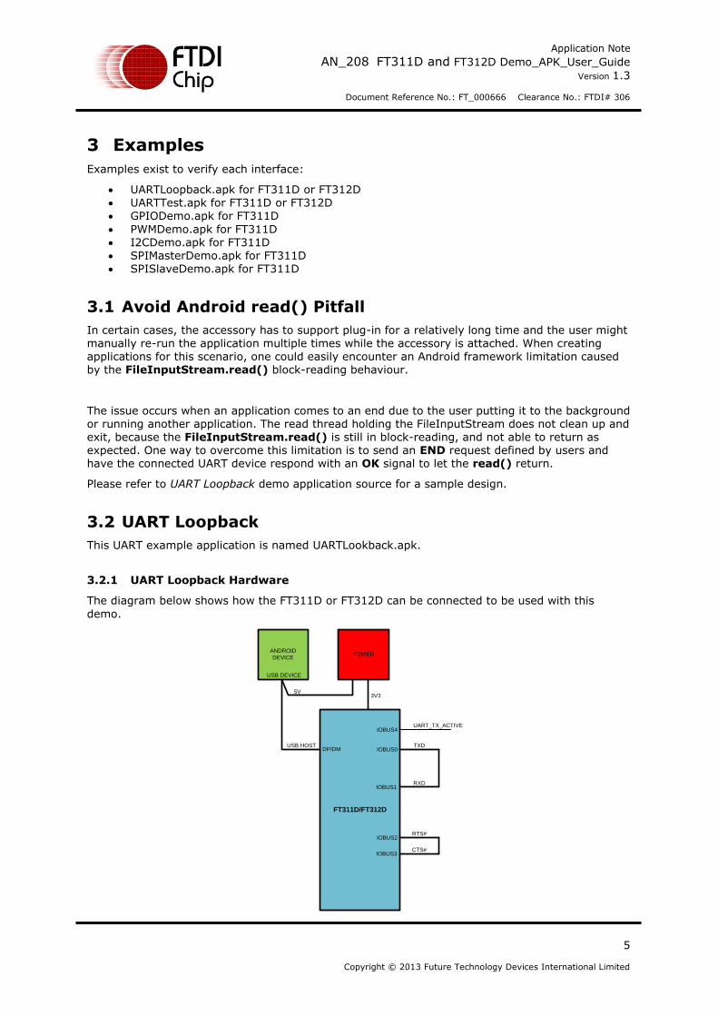
3.2.1 UART Loopback Hardware
The diagram below shows how the FT311D or FT312D can be connected to be used with this
demo.
ANDROID
DEVICE
FT311D/FT312D
USB DEVICE
USB HOSTDP/DM
POWER
5V3V3
IOBUS1
IOBUS3
IOBUS2
IOBUS4
IOBUS0
UART_TX_ACTIVE
TXD
RXD
RTS#
CTS#
Application Note
AN_208 FT311D and FT312D Demo_APK_User_Guide Version 1.3
Document Reference No.: FT_000666 Clearance No.: FTDI# 306
6
Copyright © 2013 Future Technology Devices International Limited
Figure 3.1UART Block Diagram
The block diagram represents either the FT311D or FT312D UART signals shorted together (RXD to TXD, RTS to CTS) this). This will allow data to loop in and out of the FT311D or FT3112D without
external hardware. The setup could be expanded to connect to an external UART for two way traffic. Note that the FT311D and FT312D interface operates at 3.3V levels. To connect to RS232/RS422/RS485 interfaces, an external transceiver to match the interface is required.
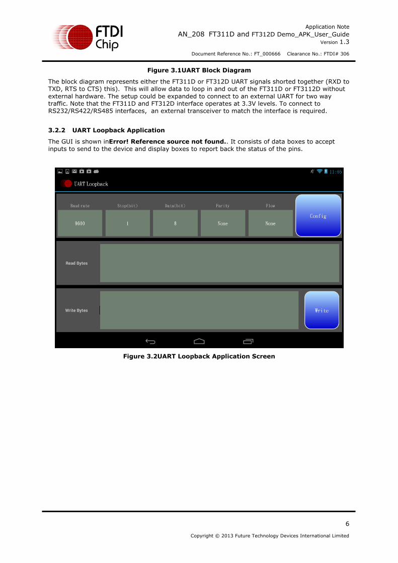
3.2.2 UART Loopback Application
The GUI is shown inError! Reference source not found.. It consists of data boxes to accept inputs to send to the device and display boxes to report back the status of the pins.
Figure 3.2UART Loopback Application Screen
Application Note
AN_208 FT311D and FT312D Demo_APK_User_Guide Version 1.3
Document Reference No.: FT_000666 Clearance No.: FTDI# 306
7
Copyright © 2013 Future Technology Devices International Limited
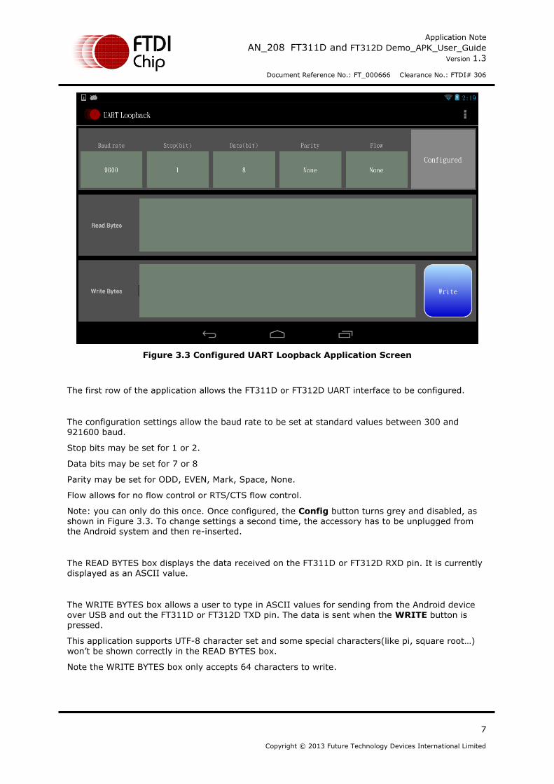
Figure 3.3 Configured UART Loopback Application Screen
The first row of the application allows the FT311D or FT312D UART interface to be configured.
The configuration settings allow the baud rate to be set at standard values between 300 and 921600 baud.
Stop bits may be set for 1 or 2.
Data bits may be set for 7 or 8
Parity may be set for ODD, EVEN, Mark, Space, None.
Flow allows for no flow control or RTS/CTS flow control.
Note: you can only do this once. Once configured, the Config button turns grey and disabled, as shown in Figure 3.3. To change settings a second time, the accessory has to be unplugged from the Android system and then re-inserted.
The READ BYTES box displays the data received on the FT311D or FT312D RXD pin. It is currently displayed as an ASCII value.
The WRITE BYTES box allows a user to type in ASCII values for sending from the Android device
over USB and out the FT311D or FT312D TXD pin. The data is sent when the WRITE button is pressed.
This application supports UTF-8 character set and some special characters(like pi, square root…)
won’t be shown correctly in the READ BYTES box.
Note the WRITE BYTES box only accepts 64 characters to write.
Application Note
AN_208 FT311D and FT312D Demo_APK_User_Guide Version 1.3
Document Reference No.: FT_000666 Clearance No.: FTDI# 306
8
Copyright © 2013 Future Technology Devices International Limited
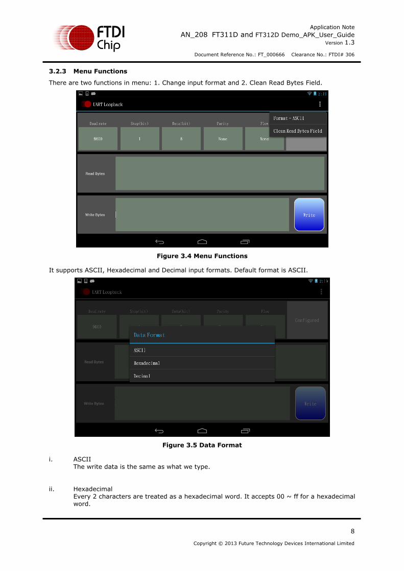
3.2.3 Menu Functions
There are two functions in menu: 1. Change input format and 2. Clean Read Bytes Field.
Figure 3.4 Menu Functions
It supports ASCII, Hexadecimal and Decimal input formats. Default format is ASCII.
Figure 3.5 Data Format
i. ASCII The write data is the same as what we type.
ii. Hexadecimal Every 2 characters are treated as a hexadecimal word. It accepts 00 ~ ff for a hexadecimal word.
Application Note
AN_208 FT311D and FT312D Demo_APK_User_Guide Version 1.3
Document Reference No.: FT_000666 Clearance No.: FTDI# 306
9
Copyright © 2013 Future Technology Devices International Limited
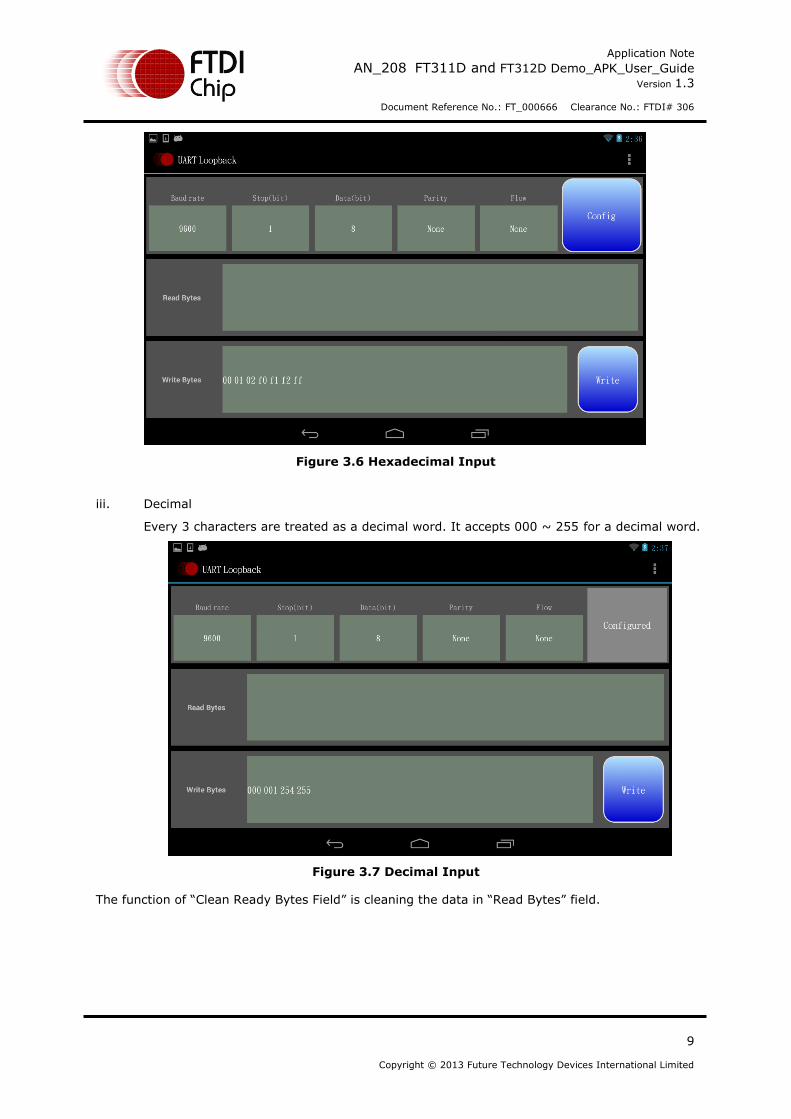
Figure 3.6 Hexadecimal Input
iii. Decimal
Every 3 characters are treated as a decimal word. It accepts 000 ~ 255 for a decimal word.
Figure 3.7 Decimal Input
The function of “Clean Ready Bytes Field” is cleaning the data in “Read Bytes” field.
Application Note
AN_208 FT311D and FT312D Demo_APK_User_Guide Version 1.3
Document Reference No.: FT_000666 Clearance No.: FTDI# 306
10
Copyright © 2013 Future Technology Devices International Limited
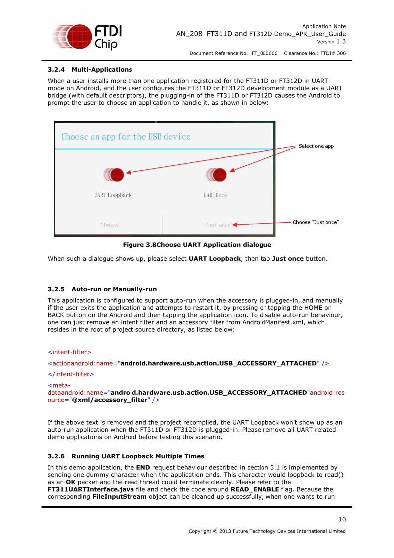
3.2.4 Multi-Applications
When a user installs more than one application registered for the FT311D or FT312D in UART mode on Android, and the user configures the FT311D or FT312D development module as a UART
bridge (with default descriptors), the plugging-in of the FT311D or FT312D causes the Android to prompt the user to choose an application to handle it, as shown in below:
Figure 3.8Choose UART Application dialogue
When such a dialogue shows up, please select UART Loopback, then tap Just once button.
3.2.5 Auto-run or Manually-run
This application is configured to support auto-run when the accessory is plugged-in, and manually if the user exits the application and attempts to restart it, by pressing or tapping the HOME or
BACK button on the Android and then tapping the application icon. To disable auto-run behaviour, one can just remove an intent filter and an accessory filter from AndroidManifest.xml, which resides in the root of project source directory, as listed below:
<intent-filter>
<actionandroid:name="android.hardware.usb.action.USB_ACCESSORY_ATTACHED" />
</intent-filter>
<meta-dataandroid:name="android.hardware.usb.action.USB_ACCESSORY_ATTACHED"android:resource="@xml/accessory_filter" />
If the above text is removed and the project recompiled, the UART Loopback won’t show up as an auto-run application when the FT311D or FT312D is plugged-in. Please remove all UART related
demo applications on Android before testing this scenario.
3.2.6 Running UART Loopback Multiple Times
In this demo application, the END request behaviour described in section 3.1 is implemented by sending one dummy character when the application ends. This character would loopback to read()
as an OK packet and the read thread could terminate cleanly. Please refer to the FT311UARTInterface.java file and check the code around READ_ENABLE flag. Because the corresponding FileInputStream object can be cleaned up successfully, when one wants to run
Application Note
AN_208 FT311D and FT312D Demo_APK_User_Guide Version 1.3
Document Reference No.: FT_000666 Clearance No.: FTDI# 306
11
Copyright © 2013 Future Technology Devices International Limited
this application again, everything can be initialized, so the demo application could run for multiple times while accessory is attached.
Application Note
AN_208 FT311D and FT312D Demo_APK_User_Guide Version 1.3
Document Reference No.: FT_000666 Clearance No.: FTDI# 306
12
Copyright © 2013 Future Technology Devices International Limited
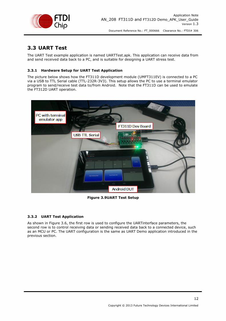
3.3 UART Test
The UART Test example application is named UARTTest.apk. This application can receive data from and send received data back to a PC, and is suitable for designing a UART stress test.
3.3.1 Hardware Setup for UART Test Application
The picture below shows how the FT311D development module (UMFT311EV) is connected to a PC via a USB to TTL Serial cable (TTL-232R-3V3). This setup allows the PC to use a terminal emulator
program to send/receive test data to/from Android. Note that the FT311D can be used to emulate the FT312D UART operation.
Figure 3.9UART Test Setup
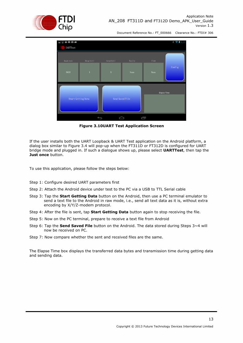
3.3.2 UART Test Application
As shown in Figure 3.6, the first row is used to configure the UARTinterface parameters, the
second row is to control receiving data or sending received data back to a connected device, such as an MCU or PC. The UART configuration is the same as UART Demo application introduced in the previous section.
Application Note
AN_208 FT311D and FT312D Demo_APK_User_Guide Version 1.3
Document Reference No.: FT_000666 Clearance No.: FTDI# 306
13
Copyright © 2013 Future Technology Devices International Limited
Figure 3.10UART Test Application Screen
If the user installs both the UART Loopback & UART Test application on the Android platform, a dialog box similar to Figure 3.4 will pop-up when the FT311D or FT312D is configured for UART bridge mode and plugged in. If such a dialogue shows up, please select UARTTest, then tap the
Just once button.
To use this application, please follow the steps below:
Step 1: Configure desired UART parameters first
Step 2: Attach the Android device under test to the PC via a USB to TTL Serial cable
Step 3: Tap the Start Getting Data button on the Android, then use a PC terminal emulator to
send a text file to the Android in raw mode, i.e., send all text data as it is, without extra encoding by X/Y/Z-modem protocol.
Step 4: After the file is sent, tap Start Getting Data button again to stop receiving the file.
Step 5: Now on the PC terminal, prepare to receive a text file from Android
Step 6: Tap the Send Saved File button on the Android. The data stored during Steps 3~4 will now be received on PC.
Step 7: Now compare whether the sent and received files are the same.
The Elapse Time box displays the transferred data bytes and transmission time during getting data and sending data.
Application Note
AN_208 FT311D and FT312D Demo_APK_User_Guide Version 1.3
Document Reference No.: FT_000666 Clearance No.: FTDI# 306
14
Copyright © 2013 Future Technology Devices International Limited
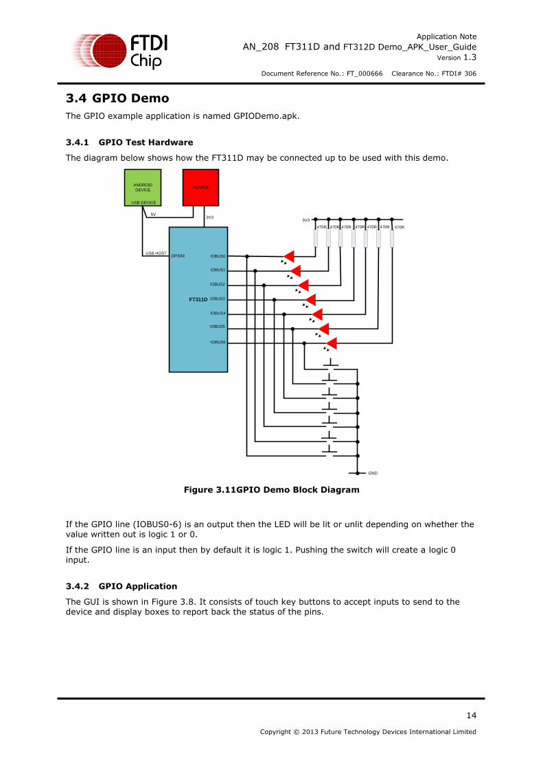
3.4 GPIO Demo
The GPIO example application is named GPIODemo.apk.
3.4.1 GPIO Test Hardware
The diagram below shows how the FT311D may be connected up to be used with this demo.
ANDROID
DEVICE
FT311D
USB DEVICE
USB HOSTDP/DM
POWER
5V3V3
3V3
470R 470R 470R 470R 470R 470R470R
IOBUS1
IOBUS3
IOBUS2
IOBUS4
IOBUS5
IOBUS6
IOBUS0
GND
Figure 3.11GPIO Demo Block Diagram
If the GPIO line (IOBUS0-6) is an output then the LED will be lit or unlit depending on whether the value written out is logic 1 or 0.
If the GPIO line is an input then by default it is logic 1. Pushing the switch will create a logic 0 input.
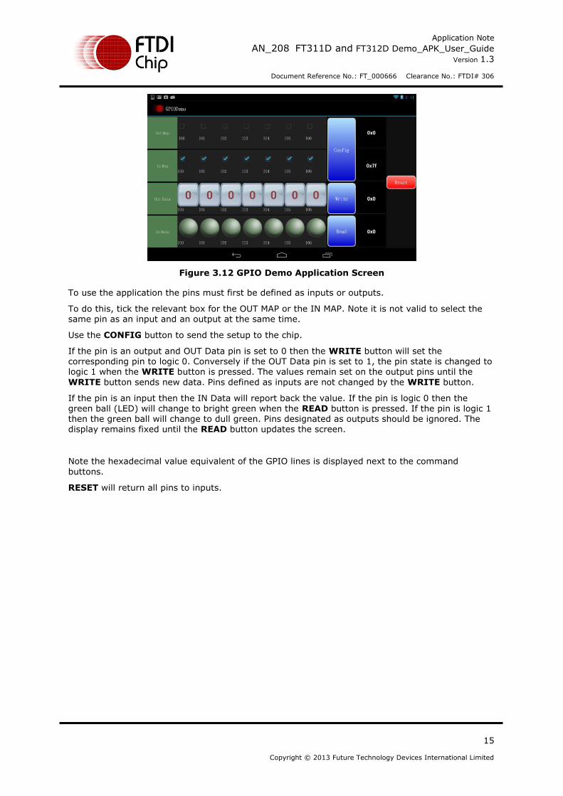
3.4.2 GPIO Application
The GUI is shown in Figure 3.8. It consists of touch key buttons to accept inputs to send to the device and display boxes to report back the status of the pins.
Application Note
AN_208 FT311D and FT312D Demo_APK_User_Guide Version 1.3
Document Reference No.: FT_000666 Clearance No.: FTDI# 306
15
Copyright © 2013 Future Technology Devices International Limited
Figure 3.12 GPIO Demo Application Screen
To use the application the pins must first be defined as inputs or outputs.
To do this, tick the relevant box for the OUT MAP or the IN MAP. Note it is not valid to select the same pin as an input and an output at the same time.
Use the CONFIG button to send the setup to the chip.
If the pin is an output and OUT Data pin is set to 0 then the WRITE button will set the corresponding pin to logic 0. Conversely if the OUT Data pin is set to 1, the pin state is changed to logic 1 when the WRITE button is pressed. The values remain set on the output pins until the
WRITE button sends new data. Pins defined as inputs are not changed by the WRITE button.
If the pin is an input then the IN Data will report back the value. If the pin is logic 0 then the green ball (LED) will change to bright green when the READ button is pressed. If the pin is logic 1 then the green ball will change to dull green. Pins designated as outputs should be ignored. The display remains fixed until the READ button updates the screen.
Note the hexadecimal value equivalent of the GPIO lines is displayed next to the command
buttons.
RESET will return all pins to inputs.
Application Note
AN_208 FT311D and FT312D Demo_APK_User_Guide Version 1.3
Document Reference No.: FT_000666 Clearance No.: FTDI# 306
16
Copyright © 2013 Future Technology Devices International Limited
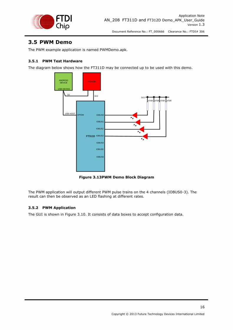
3.5 PWM Demo
The PWM example application is named PWMDemo.apk.
3.5.1 PWM Test Hardware
The diagram below shows how the FT311D may be connected up to be used with this demo.
ANDROID
DEVICE
FT311D
USB DEVICE
USB HOSTDP/DM
POWER
5V3V3
3V3
470R 470R 470R 470R
IOBUS1
IOBUS3
IOBUS2
IOBUS4
IOBUS5
IOBUS6
IOBUS0
Figure 3.13PWM Demo Block Diagram
The PWM application will output different PWM pulse trains on the 4 channels (IOBUS0-3). The result can then be observed as an LED flashing at different rates.
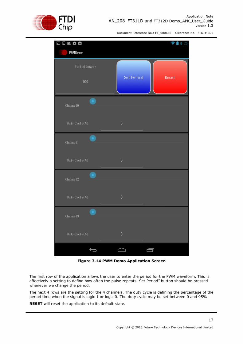
3.5.2 PWM Application
The GUI is shown in Figure 3.10. It consists of data boxes to accept configuration data.
Application Note
AN_208 FT311D and FT312D Demo_APK_User_Guide Version 1.3
Document Reference No.: FT_000666 Clearance No.: FTDI# 306
17
Copyright © 2013 Future Technology Devices International Limited
Figure 3.14 PWM Demo Application Screen
The first row of the application allows the user to enter the period for the PWM waveform. This is effectively a setting to define how often the pulse repeats. Set Period” button should be pressed whenever we change the period.
The next 4 rows are the setting for the 4 channels. The duty cycle is defining the percentage of the period time when the signal is logic 1 or logic 0. The duty cycle may be set between 0 and 95%
RESET will reset the application to its default state.
Application Note
AN_208 FT311D and FT312D Demo_APK_User_Guide Version 1.3
Document Reference No.: FT_000666 Clearance No.: FTDI# 306
18
Copyright © 2013 Future Technology Devices International Limited
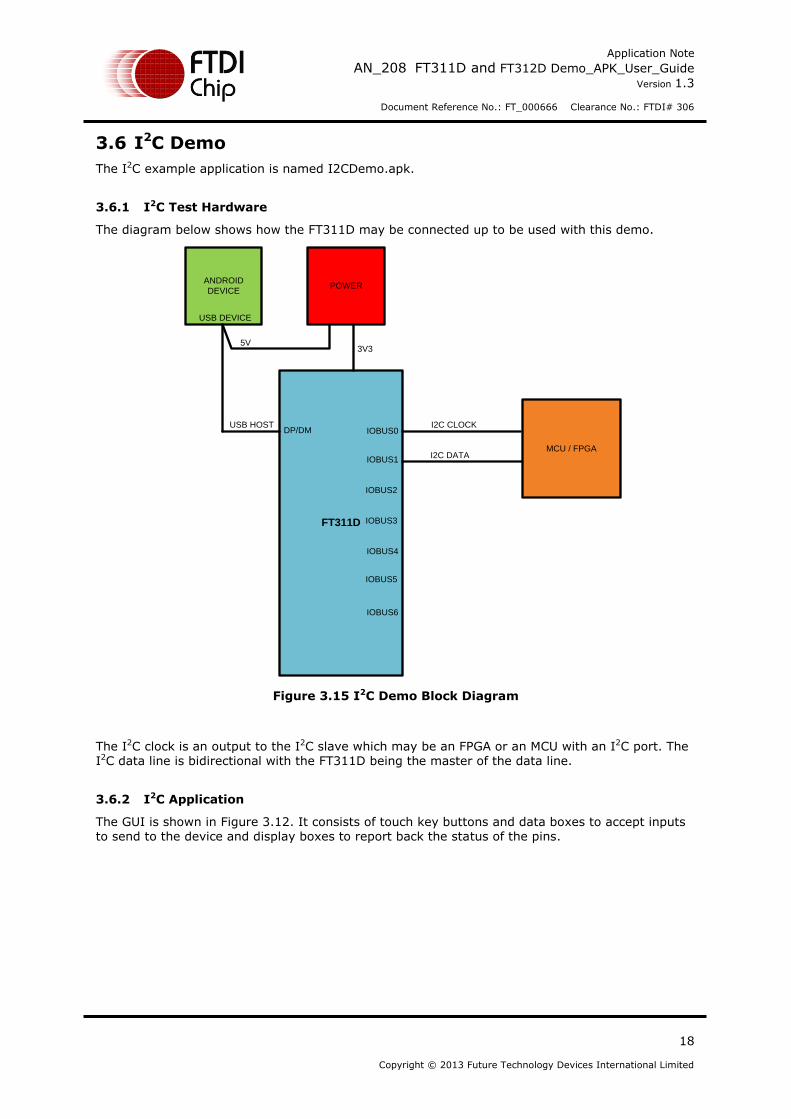
3.6 I2C Demo
The I2C example application is named I2CDemo.apk.
3.6.1 I2C Test Hardware
The diagram below shows how the FT311D may be connected up to be used with this demo.
ANDROID
DEVICE
FT311D
USB DEVICE
USB HOSTDP/DM
POWER
5V3V3
I2C CLOCK
I2C DATAIOBUS1
IOBUS3
IOBUS2
IOBUS4
IOBUS5
IOBUS6
IOBUS0
MCU / FPGA
Figure 3.15 I2C Demo Block Diagram
The I2C clock is an output to the I2C slave which may be an FPGA or an MCU with an I2C port. The I2C data line is bidirectional with the FT311D being the master of the data line.
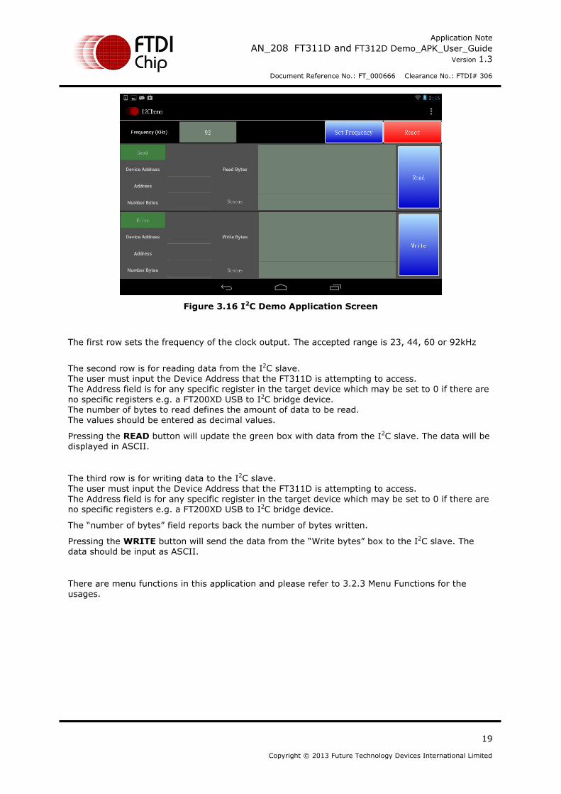
3.6.2 I2C Application
The GUI is shown in Figure 3.12. It consists of touch key buttons and data boxes to accept inputs to send to the device and display boxes to report back the status of the pins.
Application Note
AN_208 FT311D and FT312D Demo_APK_User_Guide Version 1.3
Document Reference No.: FT_000666 Clearance No.: FTDI# 306
19
Copyright © 2013 Future Technology Devices International Limited
Figure 3.16 I2C Demo Application Screen
The first row sets the frequency of the clock output. The accepted range is 23, 44, 60 or 92kHz
The second row is for reading data from the I2C slave. The user must input the Device Address that the FT311D is attempting to access. The Address field is for any specific register in the target device which may be set to 0 if there are
no specific registers e.g. a FT200XD USB to I2C bridge device. The number of bytes to read defines the amount of data to be read. The values should be entered as decimal values.
Pressing the READ button will update the green box with data from the I2C slave. The data will be
displayed in ASCII.
The third row is for writing data to the I2C slave.
The user must input the Device Address that the FT311D is attempting to access. The Address field is for any specific register in the target device which may be set to 0 if there are no specific registers e.g. a FT200XD USB to I2C bridge device.
The “number of bytes” field reports back the number of bytes written.
Pressing the WRITE button will send the data from the “Write bytes” box to the I2C slave. The data should be input as ASCII.
There are menu functions in this application and please refer to 3.2.3 Menu Functions for the usages.
Application Note
AN_208 FT311D and FT312D Demo_APK_User_Guide Version 1.3
Document Reference No.: FT_000666 Clearance No.: FTDI# 306
20
Copyright © 2013 Future Technology Devices International Limited
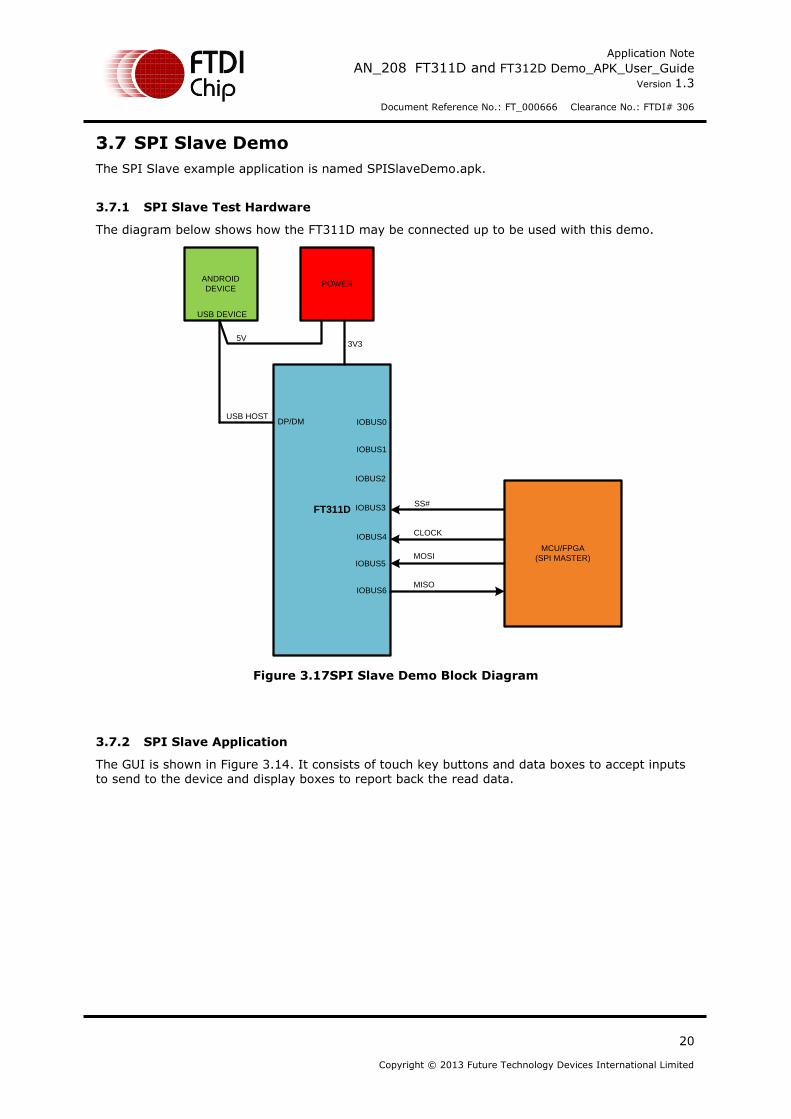
3.7 SPI Slave Demo
The SPI Slave example application is named SPISlaveDemo.apk.
3.7.1 SPI Slave Test Hardware
The diagram below shows how the FT311D may be connected up to be used with this demo.
ANDROID
DEVICE
FT311D
USB DEVICE
USB HOSTDP/DM
POWER
5V3V3
IOBUS1
IOBUS3
IOBUS2
IOBUS4
IOBUS5
IOBUS6
IOBUS0
MCU/FPGA
(SPI MASTER)
SS#
CLOCK
MISO
MOSI
Figure 3.17SPI Slave Demo Block Diagram
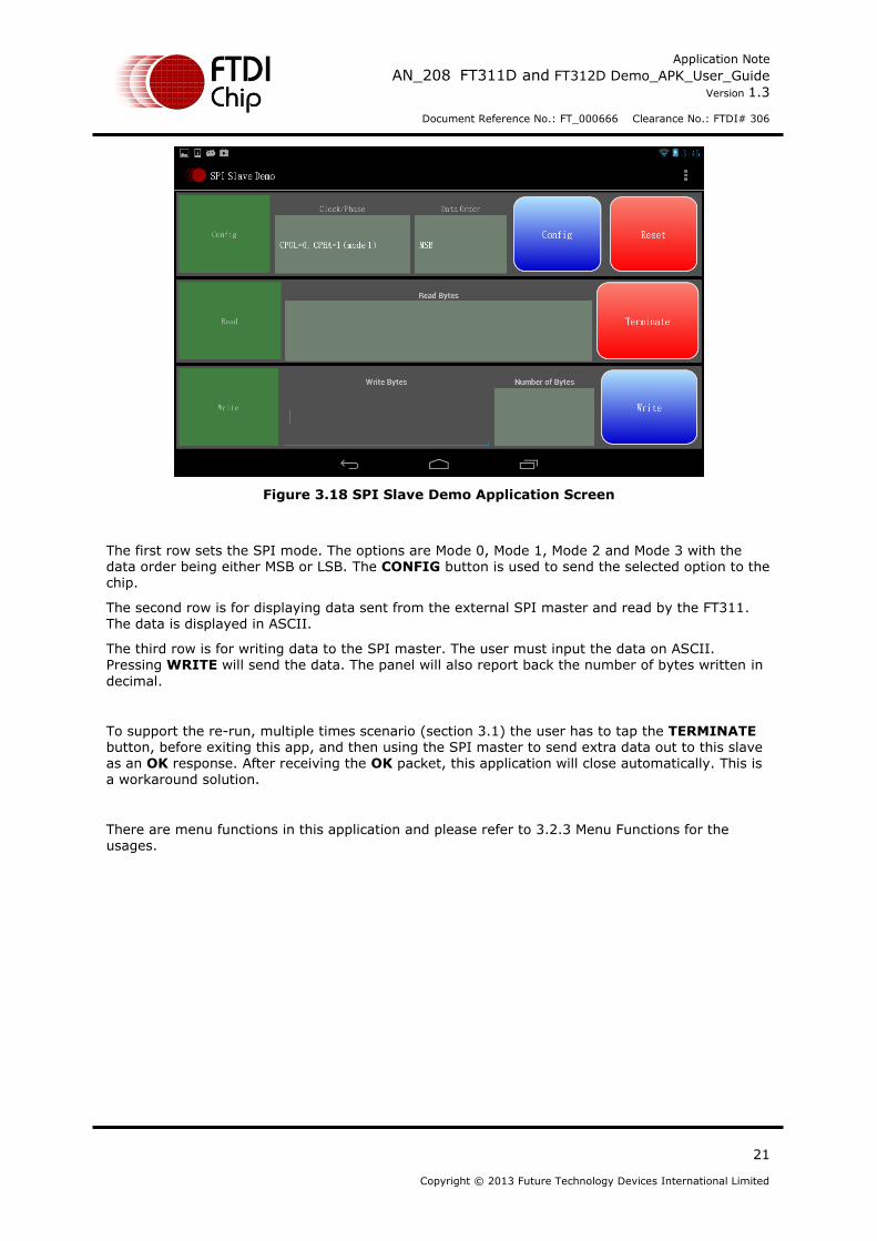
3.7.2 SPI Slave Application
The GUI is shown in Figure 3.14. It consists of touch key buttons and data boxes to accept inputs to send to the device and display boxes to report back the read data.
Application Note
AN_208 FT311D and FT312D Demo_APK_User_Guide Version 1.3
Document Reference No.: FT_000666 Clearance No.: FTDI# 306
21
Copyright © 2013 Future Technology Devices International Limited
Figure 3.18 SPI Slave Demo Application Screen
The first row sets the SPI mode. The options are Mode 0, Mode 1, Mode 2 and Mode 3 with the data order being either MSB or LSB. The CONFIG button is used to send the selected option to the chip.
The second row is for displaying data sent from the external SPI master and read by the FT311. The data is displayed in ASCII.
The third row is for writing data to the SPI master. The user must input the data on ASCII. Pressing WRITE will send the data. The panel will also report back the number of bytes written in
decimal.
To support the re-run, multiple times scenario (section 3.1) the user has to tap the TERMINATE button, before exiting this app, and then using the SPI master to send extra data out to this slave as an OK response. After receiving the OK packet, this application will close automatically. This is a workaround solution.
There are menu functions in this application and please refer to 3.2.3 Menu Functions for the usages.
Application Note
AN_208 FT311D and FT312D Demo_APK_User_Guide Version 1.3
Document Reference No.: FT_000666 Clearance No.: FTDI# 306
22
Copyright © 2013 Future Technology Devices International Limited
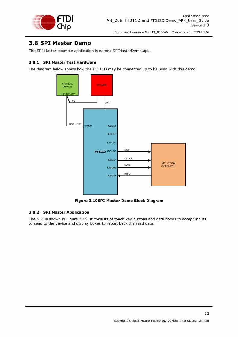
3.8 SPI Master Demo
The SPI Master example application is named SPIMasterDemo.apk.
3.8.1 SPI Master Test Hardware
The diagram below shows how the FT311D may be connected up to be used with this demo.
ANDROID
DEVICE
FT311D
USB DEVICE
USB HOSTDP/DM
POWER
5V3V3
IOBUS1
IOBUS3
IOBUS2
IOBUS4
IOBUS5
IOBUS6
IOBUS0
MCU/FPGA
(SPI SLAVE)
SS#
CLOCK
MISO
MOSI
Figure 3.19SPI Master Demo Block Diagram
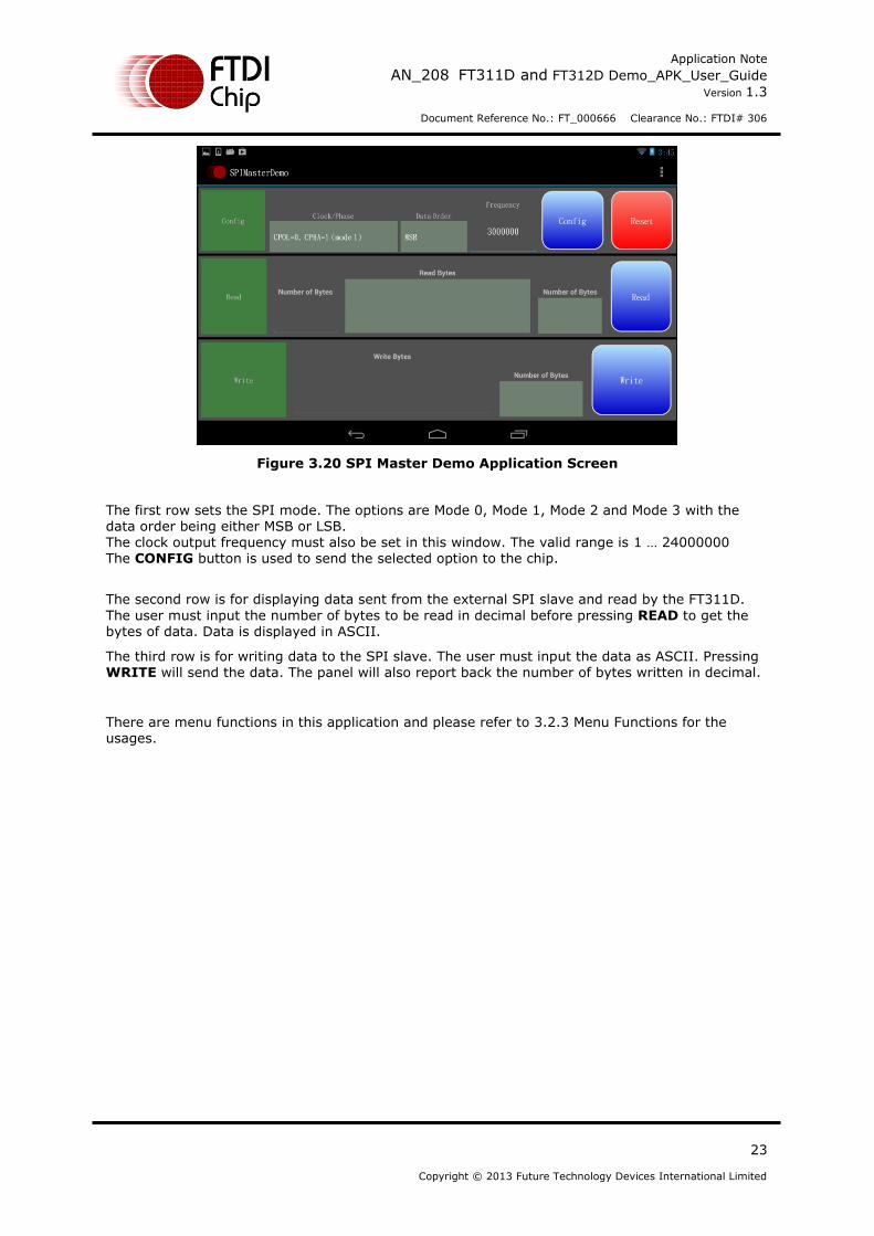
3.8.2 SPI Master Application
The GUI is shown in Figure 3.16. It consists of touch key buttons and data boxes to accept inputs to send to the device and display boxes to report back the read data.
Application Note
AN_208 FT311D and FT312D Demo_APK_User_Guide Version 1.3
Document Reference No.: FT_000666 Clearance No.: FTDI# 306
23
Copyright © 2013 Future Technology Devices International Limited
Figure 3.20 SPI Master Demo Application Screen
The first row sets the SPI mode. The options are Mode 0, Mode 1, Mode 2 and Mode 3 with the data order being either MSB or LSB. The clock output frequency must also be set in this window. The valid range is 1 … 24000000 The CONFIG button is used to send the selected option to the chip.
The second row is for displaying data sent from the external SPI slave and read by the FT311D.
The user must input the number of bytes to be read in decimal before pressing READ to get the bytes of data. Data is displayed in ASCII.
The third row is for writing data to the SPI slave. The user must input the data as ASCII. Pressing WRITE will send the data. The panel will also report back the number of bytes written in decimal.
There are menu functions in this application and please refer to 3.2.3 Menu Functions for the usages.
Application Note
AN_208 FT311D and FT312D Demo_APK_User_Guide Version 1.3
Document Reference No.: FT_000666 Clearance No.: FTDI# 306
24
Copyright © 2013 Future Technology Devices International Limited
4 Contact Information
Head Office – Glasgow, UK Unit 1, 2 Seaward Place, Centurion Business Park Glasgow G41 1HH United Kingdom Tel: +44 (0) 141 429 2777 Fax: +44 (0) 141 429 2758 E-mail (Sales) [email protected] E-mail (Support) [email protected] E-mail (General Enquiries) [email protected]
Branch Office – Taipei, Taiwan 2F, No. 516, Sec. 1, NeiHu Road Taipei 114 Taiwan , R.O.C. Tel: +886 (0) 2 8797 1330 Fax: +886 (0) 2 8751 9737 E-mail (Sales) [email protected] E-mail (Support) [email protected] E-mail (General Enquiries) [email protected]
Branch Office – Oregon, USA 7130 Fir Loop, Tigard, OR 97223-8160 USA Tel: +1 (503) 547 0988 Fax: +1 (503) 547 0987 E-Mail (Sales) [email protected] E-Mail (Support) [email protected] E-Mail (General Enquiries) [email protected]
Branch Office – Shanghai, China
Room 1103, No. 666 West Huaihai Road,
Shanghai, 200052 China Tel: +86 21 62351596 Fax: +86 21 62351595 E-mail (Sales) [email protected] E-mail (Support) [email protected] E-mail (General Enquiries) [email protected]
Web Site http://ftdichip.com
System and equipment manufacturers and designers are responsible to ensure that their systems, and any Future Technology
Devices International Ltd (FTDI) devices incorporated in their systems, meet all applicable safety, regulatory and system-level
performance requirements. All application-related information in this document (including application descriptions, suggested
FTDI devices and other materials) is provided for reference only. While FTDI has taken care to assure it is accurate, this
information is subject to customer confirmation, and FTDI disclaims all liability for system designs and for any applications
assistance provided by FTDI. Use of FTDI devices in life support and/or safety applications is entirely at the user’s risk, and the
user agrees to defend, indemnify and hold harmless FTDI from any and all damages, claims, suits or expense resulting from such use. This document is subject to change without notice. No freedom to use patents or other intellectual property rights is
implied by the publication of this document. Neither the whole nor any part of the information contained in, or the product
described in this document, may be adapted or reproduced in any material or electronic form without the prior written consent
of the copyright holder. Future Technology Devices International Ltd, Unit 1, 2 Seaward Place, Centurion Business Park,
Glasgow G41 1HH, United Kingdom. Scotland Registered Company Number: SC136640
Application Note
AN_208 FT311D and FT312D Demo_APK_User_Guide Version 1.3
Document Reference No.: FT_000666 Clearance No.: FTDI# 306
25
Copyright © 2013 Future Technology Devices International Limited
Appendix A – References
Document References
FT311D Data Sheet
FT312D Data Sheet
Acronyms and Abbreviations
Terms Description
GPIO General Purpose Input output
I2C Inter Integrated Circuit
PWM Pulse Width Modulation
SPI Serial peripheral interface
UART Universal Asynchronous Receiver Transmitter
USB Universal Serial Bus
USB-IF USB Implementers Forum
Application Note
AN_208 FT311D and FT312D Demo_APK_User_Guide Version 1.3
Document Reference No.: FT_000666 Clearance No.: FTDI# 306
26
Copyright © 2013 Future Technology Devices International Limited
Appendix B – List of Figures
List of Figures
FIGURE 3.1UART BLOCK DIAGRAM ....................................................................................................................... 6 FIGURE 3.2UART LOOPBACK APPLICATION SCREEN ............................................................................................... 6 FIGURE 3.3 CONFIGURED UART LOOPBACK APPLICATION SCREEN ....................................................................... 7 FIGURE 3.4 MENU FUNCTIONS ............................................................................................................................... 8 FIGURE 3.5 DATA FORMAT ..................................................................................................................................... 8 FIGURE 3.6 HEXADECIMAL INPUT ........................................................................................................................... 9 FIGURE 3.7 DECIMAL INPUT ................................................................................................................................... 9 FIGURE 3.8CHOOSE UART APPLICATION DIALOGUE ............................................................................................ 10 FIGURE 3.9UART TEST SETUP ............................................................................................................................... 12 FIGURE 3.10UART TEST APPLICATION SCREEN ..................................................................................................... 13 FIGURE 3.11GPIO DEMO BLOCK DIAGRAM .......................................................................................................... 14 FIGURE 3.12 GPIO DEMO APPLICATION SCREEN .................................................................................................. 15 FIGURE 3.13PWM DEMO BLOCK DIAGRAM ......................................................................................................... 16 FIGURE 3.14 PWM DEMO APPLICATION SCREEN ................................................................................................. 17 FIGURE 3.15 I
2C DEMO BLOCK DIAGRAM ............................................................................................................. 18
FIGURE 3.16 I2C DEMO APPLICATION SCREEN...................................................................................................... 19
FIGURE 3.17SPI SLAVE DEMO BLOCK DIAGRAM .................................................................................................. 20 FIGURE 3.18 SPI SLAVE DEMO APPLICATION SCREEN .......................................................................................... 21 FIGURE 3.19SPI MASTER DEMO BLOCK DIAGRAM ............................................................................................... 22 FIGURE 3.20 SPI MASTER DEMO APPLICATION SCREEN ....................................................................................... 23
Application Note
AN_208 FT311D and FT312D Demo_APK_User_Guide Version 1.3
Document Reference No.: FT_000666 Clearance No.: FTDI# 306
27
Copyright © 2013 Future Technology Devices International Limited
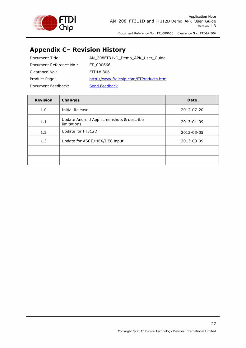
Appendix C– Revision History
Document Title: AN_208FT31xD_Demo_APK_User_Guide
Document Reference No.: FT_000666
Clearance No.: FTDI# 306
Product Page: http://www.ftdichip.com/FTProducts.htm
Document Feedback: Send Feedback
Revision Changes Date
1.0 Initial Release 2012-07-20
1.1 Update Android App screenshots & describe limitations
2013-01-09
1.2 Update for FT312D 2013-03-05
1.3 Update for ASCII/HEX/DEC input 2013-09-09