from technologies to market - system plus consulting · • microled display application...
TRANSCRIPT

© 2017
From Technologies to Market
MicroLEDDisplays:
Hype and reality, hopes and challenges
From Technologies to Market
Picture: SonySample
©2017
2
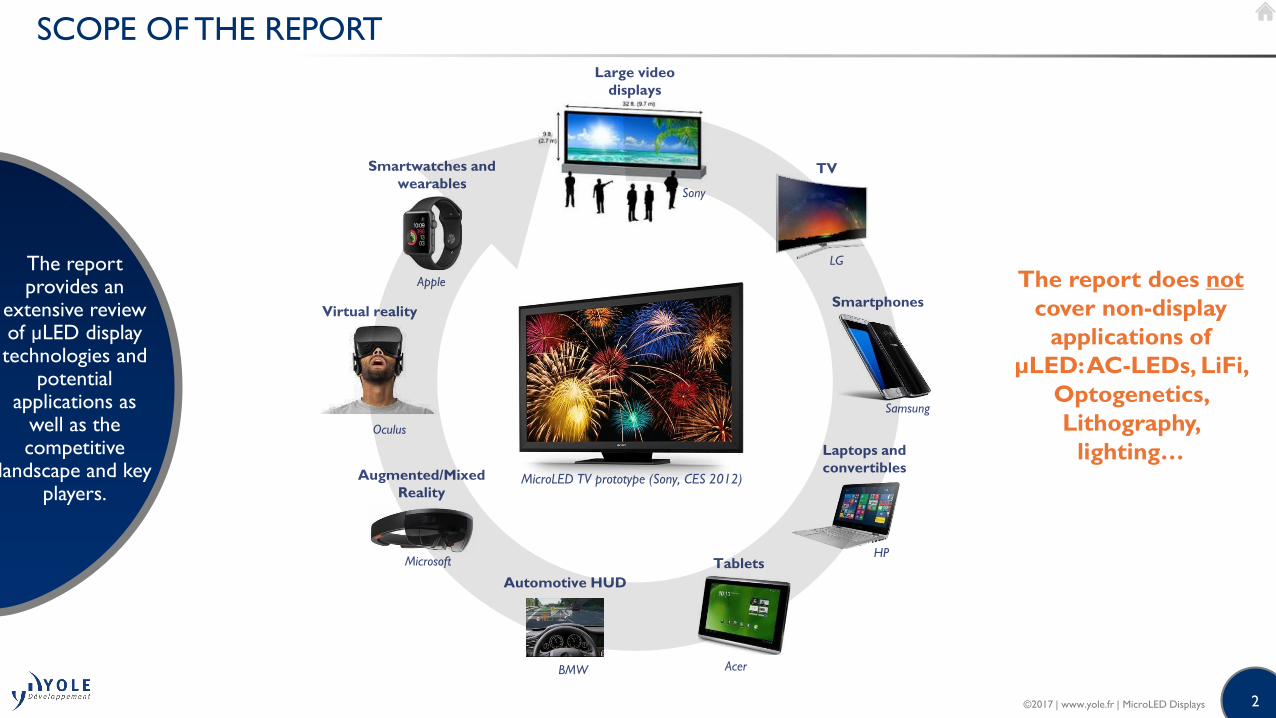
SCOPE OF THE REPORT
The report provides an
extensive review of µLED display technologies and
potential applications as
well as the competitive
landscape and key players.
Smartwatches and
wearables
Virtual reality
Large video
displays
TV
Smartphones
Laptops and
convertibles
Automotive HUD
Augmented/Mixed
Reality
Sony
LG
Samsung
HP
BMW
Microsoft
Oculus
Apple
Tablets
Acer
The report does not
cover non-display
applications of
µLED: AC-LEDs, LiFi,
Optogenetics,
Lithography,
lighting…MicroLED TV prototype (Sony, CES 2012)
©2017 | www.yole.fr | MicroLED Displays
3
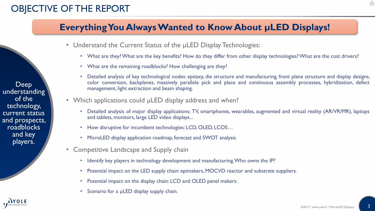
OBJECTIVE OF THE REPORT
Deep understanding
of the technology,
current status and prospects,
roadblocks and key players.
• Understand the Current Status of the µLED Display Technologies:
• What are they? What are the key benefits? How do they differ from other display technologies?What are the cost drivers?
• What are the remaining roadblocks? How challenging are they?
• Detailed analysis of key technological nodes: epitaxy, die structure and manufacturing, front plane structure and display designs,color conversion, backplanes, massively parallele pick and place and continuous assembly processes, hybridization, defectmanagement, light extraction and beam shaping.
• Which applications could µLED display address and when?
• Detailed analysis of major display applications: TV, smartphones, wearables, augmented and virtual reality (AR/VR/MR), laptopsand tablets, monitors, large LED video displays...
• How disruptive for incumbent technologies: LCD, OLED, LCOS…
• MicroLED display application roadmap, forecast and SWOT analysis
• Competitive Landscape and Supply chain
• Identify key players in technology development and manufacturing.Who owns the IP?
• Potential impact on the LED supply chain: epimakers, MOCVD reactor and substrate suppliers.
• Potential impact on the display chain: LCD and OLED panel makers.
• Scenario for a µLED display supply chain.
Everything You Always Wanted to Know About µLED Displays!
©2017 | www.yole.fr | MicroLED Displays

4
REPORT METHODOLOGY
Market segmentation methodology
Market forecast methodology
©2017 | www.yole.fr | MicroLED Displays

5
REPORT METHODOLOGY
Technology analysis methodology Information collection
©2017 | www.yole.fr | MicroLED Displays
6
TABLE OF CONTENTS
• Scope Of the Report p8
• Objective Of the Report p9
• Who should Be Interested In this Report? p10
• Companies cited in the report p11
• Acronyms p12
• Executive Summary p13
• What is a MicroLED displays?
• Status
• Remaining Roadblocks
• MicroLED Attributes vs Application Requirement
• SWOT Analysis
• Major Technology Bricks
• Assembly Technologies
• Display Structure and Backplane
• MicroLED efficiency
• MicroLED Dimensions
• Epitaxy
• Chip Manufacturing
• Color Conversion
• Cost Drivers
• Defect Management
• Major Players
• Supply chain
• Possible Winner and Losers.
• MicroLED Application Roadmap
• 2017-2025 MicroLED Adoption Forecast
• What’s Happening In the Short Term?
• Introduction p52
• LED Efficiency
• Display Resolutions
• OLED and LCD Display structure Overview
• Display Trends
• LEDs In displays
• MicroLED Definition and History
• MicroLED Displays Technology Evolution
• What is a MicroLED displays?
• MicroLED Display Assembly
• MicroLED Chip Manufacturing
• Benefits
• Comparisons With LCD and OLED
• MicroLED Display Manufacturing Challenges
• MicroLED Displays Frontplane & Pixel Structures p68
• Backplane and Pixel Bank Structure
• MicroLED Display Structure: Monochrome
• MicroLED Display Structure: Color
• Pixel Fill Factor and Added Display Functionalities
• Pixel density and Pixel Pitch
• Subassembly Microsystems
• Tiled Arrays
• LED Efficiency
• Brightness
• Pixel Size vs. Efficiency
• MicroLED Driving Regime
©2017 | www.yole.fr | MicroLED Displays

7
TABLE OF CONTENTS
©2017 | www.yole.fr | MicroLED Displays
• Ultra High Brightness MicroDisplays
• MicroLED Large video displays
• Current confinement Trenches
• MicroLED efficiency
• MicroLED Dimensions
• MicroLED Displays Backplanes p91
• Passive Matrix Driving
• Active Matrix Driving
• LCD vs Emissive display Driving Requirement
• Emissive Display Driving
• Thin Film Transistor Backplanes
• TFT Substrates Example: Gen 10
• TFT Channel Material
• Trends
• Channel Materials For MicroLED Displays
• Pixel Density and Backplane
• Impact on MicroLED Driving Technology
• Impact on MicroLED Assembly Technology
• Discrete Micro-Controllers
• MicroLED Epitaxy p106(Front End Level 0)
• Overview
• Epitaxy Defects and Dead Pixels
• Wavelength homogeneity and Consistency
• Brightness and Voltage Variations
• Impact on Supply chain
• Chip Manufacturing and Singulation p115(front End Level 1)
• Chip singulation:
• Bonding and Etching: Apple-Luxvue
• Anchor and Breakable Tethers: X-Celeprint
• Chip Manufacturing
• Impact on Supply chain
• Transfer And Assembly Technologies p125
• Pick and Place vs Monolithic Arrays
• Massively Parallel Pick and Place and Printing Processes p127
• Overview
• Transfer Sequences
• Transfer Array Vs. Display Pixel Pitch
• Throughput and cost Drivers
• Edge Effects
• Pick and Place Processes
• Die Stabilization and Release.
• Die Selection
• Pick Up Methods
• Luxvue: Electrostatic MEMS
• Luxvue Compliant Pick Up Heads
• Luxvue Transfer Process Sequence
• Luxvue Alternative Process
• X-Celeprint Elastomere Transfer Printing
• Other Process Flows: Die Encapsulation
• Other Process Flows: Stretchable Film
• Semi-continuous Process
8
TABLE OF CONTENTS
©2017 | www.yole.fr | MicroLED Displays
• Wet Printing, Electrophotographic
• Fluidic Assembly
• Key IP Holders and Conclusion
• Large Monolithic MicroLED Arrays p160
• The challenge for High Pixel Density
• Full Array Level Microdisplay Manufacturing.
• Hybridization
• MicroLED Array Hybridization on CMOS: LETI
• Monolithic Integration of LTPS TFT: Lumiode
• Monolithic Integration of Metal Oxide TFT: eMagin
• Monolithic Integration of GaN TFT: OSRAM and Nth Degree
• Micro-wire MicroLED Arrays: Aledia
• 3D Integration: Ostendo
• Conclusion
• Light Extraction and Viewing Angles p175
• Introduction
• Die-Level Beam Shaping and Extraction
• Illustration: InfiniLED
• Array-Level Beam Shaping
• External Micro Optics
• Viewing Angle and Power consumption
• Color Conversion p183
• Color Gamut
• Comparison of major standards
• Major Color Gamut in the CIE 1931 and 1976 spaces
• Color Conversion
• Wavelength Converter Deposition
• Broadband phosphors
• Narrowband Phosphors
• Examples
• Phosphors Particle size
• Quantum Dots
• Benefits and challenges
• Performance
• Implementations in Traditional Displays
• Challenges for MicroLED Displays
• QD vs Phosphors: Summary
• Quantum Wells converters.
• Defect Management p201
• Introduction
• Bad Pixels
• Emitter Redundancy
• Example of Repair Strategies
• Defect Management Strategies
• Conclusion
• Applications and Markets for MicroLED Displays p212
• Overview Of Key Hypothesis
• Overview of Epiwafer Cost per Application
• Overview of Epiwafer And Transfer Cost per Application
• Discussion
• MicroLED Attributes vs Application Requirement
• MicroLED Application Roadmap
• MicroLED SWOT Per Application
• 2017-2025 MicroLED Adoption Forecast

9
TABLE OF CONTENTS
©2017 | www.yole.fr | MicroLED Displays
• Virtual Reality p224
• Introduction: VR and AR/MR
• The Reality-to-Virtual-Reality Continuum.
• VR Displays: FOV, Resolution and Pixel Density
• VR Displays: Refresh Rate
• VR Displays: Brightness
• Computing Power and Bandwidth
• Foveated rendering
• Trade Offs for the Design of a VR Headset
• Current status
• Microdisplays
• MicroLED displays for VR: Transfer-Based (Large displays)
• Screen Door Effect
• MicroLED Microdisplays
• MicroLED displays for VR: conclusion
• Augmented and Mixed Reality p244
• Display Requirements
• Display Types:
• MicroLED Displays for AR and MR
• Comparison of AR Displays Technologies
• 2017 – 2027 AR/MR Market Forecast
• 2020-2027 MicroLED Scenario for AR/MR.
• Head Up displays
• 2020-2025 MicroLED Head Up displays Forecast
• Smartwatches p253
• Introduction
• Forecasting the Smartwatch market
• MicroLED for Smartwatches
• 2017-2025 Forecast
• MOCVD Requirement
• Transfer Tools Requirements
• TVs p262
• Introduction
• The UHD alliance
• MicroLED vs OLED and QD-LCD
• MicroLED TV Panel costs
• Additional Challenges For MicroLED TVs
• MicroLED Volume forecast and MOCVD Requirements
• Transfer Tools Requirements
• Alternative Transfer and Assembly Approaches
• Smart Phones p273
• Smartphone display Requirement
• Is 4K required?
• MicroLED for Cell Phones: Epiwafer Cost
• MicroLED for Cell Phones: Transfer Cost
• No Pixel Redundancy
• Pixel Redundancy
• Status and roadblocks
• 2017-2025 Volume forecast and MOCVD Requirements
• Transfer Tools Requirements
• Tablets p284
• MicroLED Tablet Panel costs
• 2017-2025 Volume forecast and MOCVD Requirements
• Transfer Tools Requirements
10
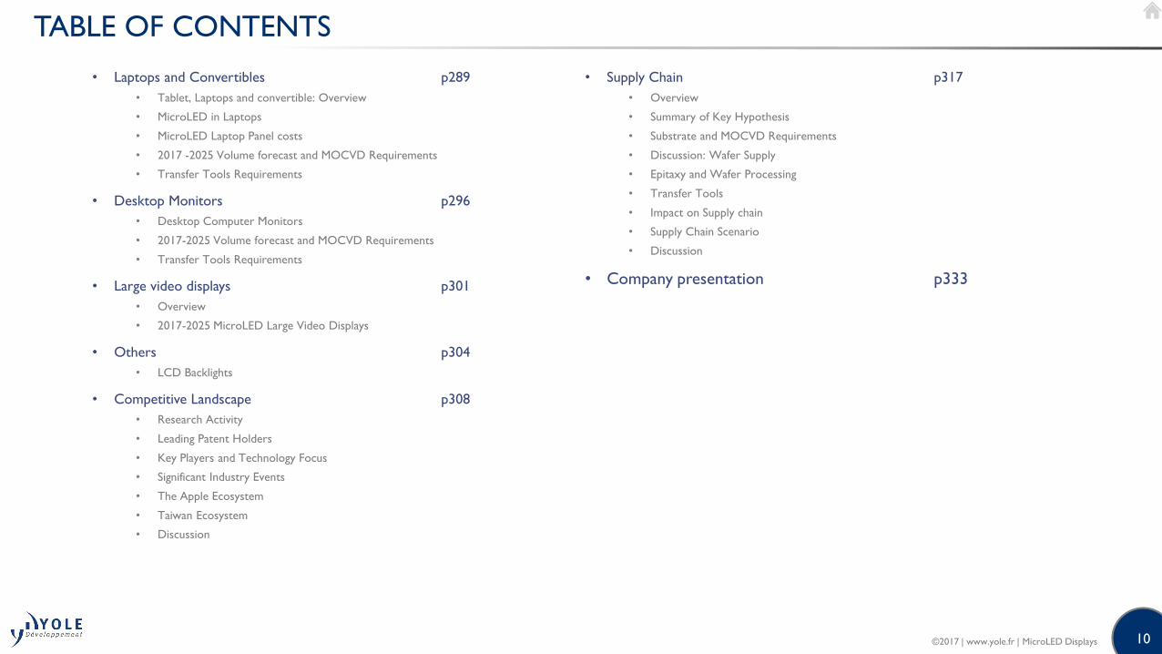
TABLE OF CONTENTS
©2017 | www.yole.fr | MicroLED Displays
• Laptops and Convertibles p289
• Tablet, Laptops and convertible: Overview
• MicroLED in Laptops
• MicroLED Laptop Panel costs
• 2017 -2025 Volume forecast and MOCVD Requirements
• Transfer Tools Requirements
• Desktop Monitors p296
• Desktop Computer Monitors
• 2017-2025 Volume forecast and MOCVD Requirements
• Transfer Tools Requirements
• Large video displays p301
• Overview
• 2017-2025 MicroLED Large Video Displays
• Others p304
• LCD Backlights
• Competitive Landscape p308
• Research Activity
• Leading Patent Holders
• Key Players and Technology Focus
• Significant Industry Events
• The Apple Ecosystem
• Taiwan Ecosystem
• Discussion
• Supply Chain p317
• Overview
• Summary of Key Hypothesis
• Substrate and MOCVD Requirements
• Discussion: Wafer Supply
• Epitaxy and Wafer Processing
• Transfer Tools
• Impact on Supply chain
• Supply Chain Scenario
• Discussion
• Company presentation p333

11
ACRONYMS
• AR:Augmented Reality
• CapEx: Capital Expenditure
• CMOS: Complementary Metal Oxide Semiconductor
• EQE: External Quantum Efficiency
• FET: Field Effect Transistor
• FHD: Full High Definition (1920 x 1080)
• FOV: Field OfView
• FWHM: Full Width at Half Maximum
• HD: High Definition
• HMD: Head Mounted Display
• HUD: Head Up Display
• IC: Integrated Circuit
• IQE: Internal Quantum Efficiency
• LCD: Liquid Crystal Display
• LCOS: Liquid Crystal On Silicon
• LED: Light Emitting Diode
• LTPS: Low Temperature Polysilicon
• MEMS: Micro Electro-Mechanical Systems
• MOCVD: Metal-Oxide ChemicalVapor Deposition
• MR: Mixed Reality
• ODM: Original Design Manufacturer
• OEE: Optical Extraction Efficiency
• OEM: Original Equipment Manufacturer
• OLED: Organic Light emitting Diode
• PDMS: Polydimethylsiloxane (polymer material)
• PECVD: Plasma-Enhanced ChemicalVapor Deposition
• P&P: Pick and Place
• PPD: Pixel Per Degree
• PPI: Pixel Per Inch
• PPM: Parts Per Million
• QD: Quantum Dots
• QHD: Quad High Definition (2560 x 1400 to 3440 x 1440)
• TFT:Thin Film Transi
©2017 | www.yole.fr | MicroLED Displays

12
WHO SHOULD BE INTERESTED IN THIS REPORT
• LED supply chain: sapphire makers, MOCVD
suppliers, epi-houses.
• Understand the µLED display opportunity
• What does it entail for the LED supply?
• What are the technical challenges?
• How can my company participate in this emerging
opportunity?
• Who should we partner with?
• R&D Organizations and Universities
• Understand the market potential of your
technologies for this emerging market
• Identify the best candidates for collaboration and
technology transfer.
• OEMs / ODMs
• What are the potential benefits of µLED displays?
• Are they a threat or an opportunity for my
products?
• When will they be ready
• Should I get involved in the supply chain.
• Display Makers and supply chain
• Hype versus reality: what is the status of µLEDdisplays? What can we expect in the nearfuture?
• Are they a threat to my LCD and OLEDinvestments?
• Which display applications and markets canµLED displays address? A detailed roadmap.
• Find the right partner: detailed mapping of theµLED ecosystem and supply chain
• OSAT and foundries
• Are µLED a new opportunity for mycompany?
• Venture capital, financial and strategicinvestors.
• Hype versus reality. Understand thetechnology and the real potential.
• How is the supply chain shaping up?
• Identify the key players and potentialinvestment targets.
• Could µLED hurt my existing investments?
©2017 | www.yole.fr | MicroLED Displays

13
COMPANIES CITED IN THE REPORT
Aledia (FR), Allos Semiconductor (DE), Apple (US), AUO (TW), BOE (CN), CEA-LETI (FR), CIOMP
(CN), Columbia University (US), Cooledge (CA), Cree (US), CSOT (CN), eMagin (US), Epistar (TW),
Epson (JP), Facebook (US), Foxconn (TW), Fraunhofer Institute (DE), Glo (SE), GlobalFoundries (US),
Goertek (CN), Hiphoton (TW), HKUST (HK), HTC (TW), Ignis (CA), InfiniLED (UK), Intel (US), ITRI
(TW), Kansas State University (US), Kopin (US), Lumiode (US), Luxvue (US), Metavision (US), Microsoft
(US), Mikro-Mesa (TW), mLED (UK), Nichia (JP), Nth Degree (US), Oculus (US), Osterhout Design
Group (US), Osram (DE), Ostendo (US), Playnitride (TW), PSI Co (KR), Rohinni (US), Saitama
University (JP), Samsung (KR), Sanan (CN), Semprius (US), Sharp (JP), Sony (JP), Strathclyde University
(UK), SunYat-Sen University (TW),Texas Tech (US),TSMC (TW), Tyndall National Institute (IE),
University of Illinois (US),VerLASE (US),VueReal (CA),Vuzix (US), X-Celeprint (IE).
©2017 | www.yole.fr | MicroLED Displays

14
Biography & contact
ABOUT THE AUTHOR
©2017 | www.yole.fr | MicroLED Displays
• LED Packaging
• LED Front End Manufacturing
• III-V Epitaxy
• Bulk GaN
• GaN on Silicon
• Status of the LED Industry
• Sapphire Market & Applications
• Phosphors and Quantum Dots
• OrganicTFTs
• …
Contact: [email protected]
Eric Virey is a Senior Market and Technology Analyst at Yole Développement. Eric is a daily contributor to thedevelopment of LED, OLED, and Displays activities at Yole, with a large collection of market and technologyreports as well as multiple custom consulting projects: business strategy, identification of investments oracquisition targets, due diligences (buy/sell side), market and technology analysis, cost modelling, technologyscouting, etc. Thanks to its deep knowledge of the LED/OLED and displays related industries, Eric has spoken inmore than 30 industry conferences worldwide over the last 5 years. He has been interviewed and quoted byleading media over the world.
Previously Eric has held various R&D, engineering, manufacturing and business development positions withFortune 500 Company Saint-Gobain in France and the United States.
Dr Eric Virey holds a Ph-D in Optoelectronics from the National Polytechnic Institute of GrenobleEric is alsoauthor / co-author of multiple reports (examples below) and contributed to various custom projects.


16
LEDS IN DISPLAYS
• Traditional SMD or CSP packaged LEDs are commonly used as the illumination source for the backlighting of LCD
panels.
• LEDs are also commonly used in large direct emissive video billboards used in stadium, advertising and video facades.
In those devices, discrete packaged LED containing red, green and blue chips form the individual pixels with pitches
typically ranging from 1 to 40 mm depending on display size and resolution.
• As of Q1-2017, there is no other format of commercial displays using LEDs as a direct emissive element to
constitute individual pixels or sub-pixels. The reasons for this limitation are multiple and include cost and
manufacturability.
• Nevertheless, the idea of µLED displays with high resolution and sub millimetric pixel pitch is almost as old as the
invention and commercialization of LEDs themselves. Over the last 3-4 years it has generated a lot of excitement and
development as well as investment and M&A activity.
Packaged LEDs are commonly used in large video displays and LCD backlight. MicroLEDs could be at the center of a new display revolution
©2017 | www.yole.fr | MicroLED Displays
Illustration: www.absen.com
Packaged LED
LED Video display

17
MICROLED APPLICATION ROADMAP
Soon)
(2-3 years)Longer term (>5 years)
or out of reach?
Mid term
(3-5 year)Now
(2017)
Small pitch (<2 mm)
large video displays.
• Brings significant
performance improvement
(contrast) and potential
cost reduction (eliminates
LED package)
• Large die OK (30 µm) but
low transfer efficiency.
• Available from Sony in
2017:
Detailed roadmap in the
report
©2017 | www.yole.fr | MicroLED Displays
18
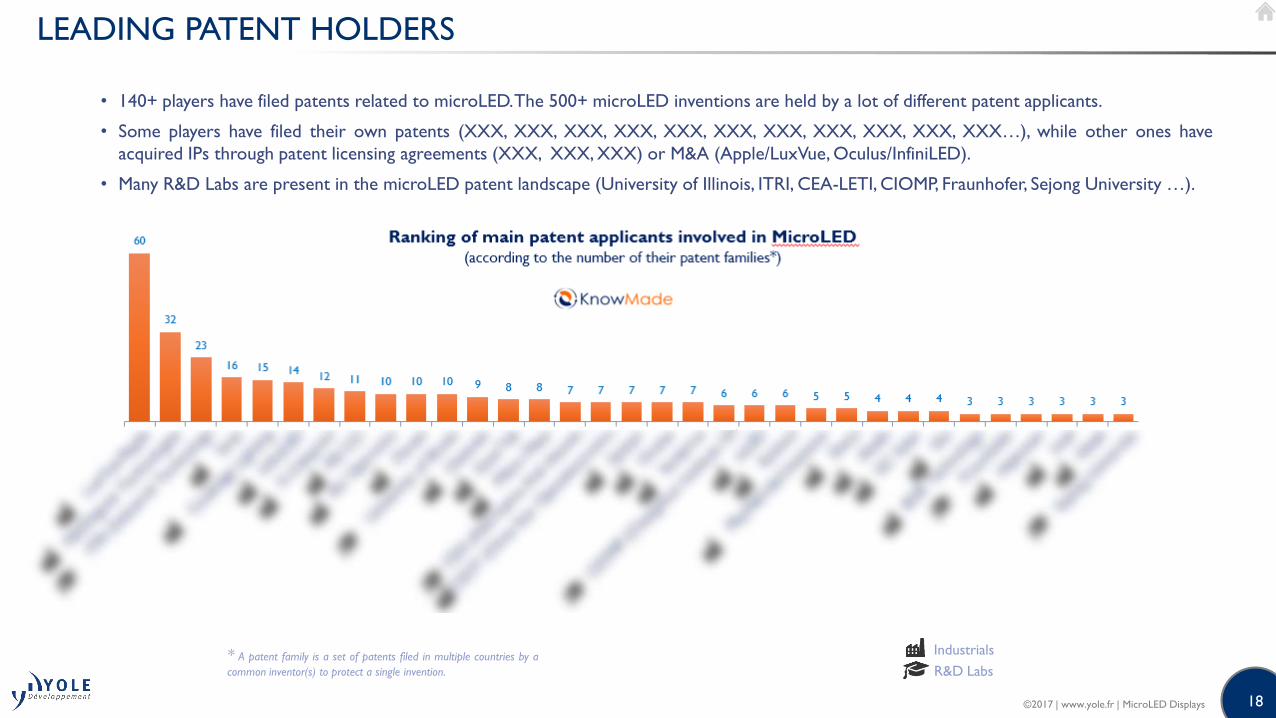
LEADING PATENT HOLDERS
©2017 | www.yole.fr | MicroLED Displays
* A patent family is a set of patents filed in multiple countries by a
common inventor(s) to protect a single invention.
Industrials
R&D Labs
• 140+ players have filed patents related to microLED.The 500+ microLED inventions are held by a lot of different patent applicants.
• Some players have filed their own patents (XXX, XXX, XXX, XXX, XXX, XXX, XXX, XXX, XXX, XXX, XXX…), while other ones have
acquired IPs through patent licensing agreements (XXX, XXX, XXX) or M&A (Apple/LuxVue, Oculus/InfiniLED).
• Many R&D Labs are present in the microLED patent landscape (University of Illinois, ITRI, CEA-LETI, CIOMP, Fraunhofer, Sejong University …).

19
MAJOR PLAYERS
©2017 | www.yole.fr | MicroLED Displays
EpitaxyµLED
structure
Transfer and
interconnectHybridization
Testing and
repair / Defect
Management
Color
Conversion
Light Extraction
& shaping
Display
architecture &
drivers
Details in the report
20
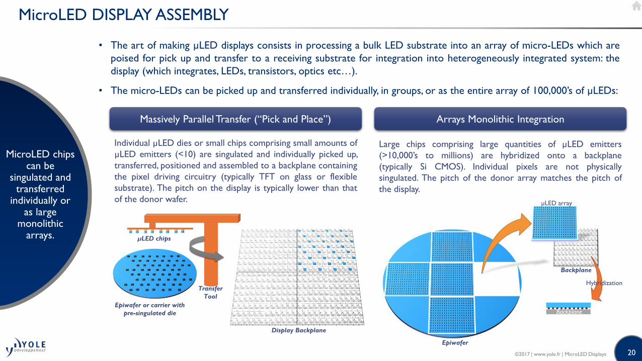
MicroLED DISPLAY ASSEMBLY
• The art of making µLED displays consists in processing a bulk LED substrate into an array of micro-LEDs which are
poised for pick up and transfer to a receiving substrate for integration into heterogeneously integrated system: the
display (which integrates, LEDs, transistors, optics etc…).
• The micro-LEDs can be picked up and transferred individually, in groups, or as the entire array of 100,000’s of µLEDs:
MicroLED chips can be
singulated and transferred
individually or as large
monolithic arrays.
Massively Parallel Transfer (“Pick and Place”) Arrays Monolithic Integration
Individual µLED dies or small chips comprising small amounts of
µLED emitters (<10) are singulated and individually picked up,
transferred, positioned and assembled to a backplane containing
the pixel driving circuitry (typically TFT on glass or flexible
substrate). The pitch on the display is typically lower than that
of the donor wafer.
Large chips comprising large quantities of µLED emitters
(>10,000’s to millions) are hybridized onto a backplane
(typically Si CMOS). Individual pixels are not physically
singulated. The pitch of the donor array matches the pitch of
the display.
Epiwafer or carrier with
pre-singulated die
Transfer
Tool
Display Backplane
µLED chips
Backplane
µLED array
Epiwafer
Backplane
Hybridization
©2017 | www.yole.fr | MicroLED Displays

21
BACKPLANE AND PIXEL BANK STRUCTURE
• The front plane structure
including the interconnects
and the pixel banks can be
built directly upon the
backplane.
• The bank layer thickness
and angle can be used to
adjust the display viewing
angle. µLED dies are
positioned into the pixel
bank by the transfer tool
and connected by solder
reflow or other processes.
• More than 1 µLED of the
same color can be placed in
each bank if redundancy is
required to mitigate risks of
dead/malfunctioning pixels
(see “Defect Management”
section of this report)
The TFT backplane can be essentially
identical to that of an OLED
display all the way through the
planarization layer.
©2017 | www.yole.fr | MicroLED Displays
Passivation
Gate(metal)
Backplane substrate (Glass, metal, plastic)
Gate Insulator
Channel (semiconductor)Drain Source
Gate Insulator (Dielectric)
Planarization Layer
(Also known as Interlayer Dielectric: ILD)
Electrode
to pixel
Cross section of a microLED display subpixel
Bottom electrodeBank layer
Other circuitry (not detailed): switch
transistors, compensation transistors,
capacitors,
Passivation
Transparent electrode
Bac
kpla
ne
Fro
ntp
lane
Light
Simplified top view of the pixel bank
Subpixel
bank
Sub
pixel
Pixel bank

22
EXAMPLE OF TRANSFER SEQUENCES
©2017 | www.yole.fr | MicroLED Displays
1)
2)
3)
4)
Transfer sequence to populate a 8x8 monochromatic display from a single donor wafer in 4 steps.
Donor wafer Donor wafer
Transfer array
Transfer array
Transfer array
Transfer arrayDisplay substrate
Display substrate
Display substrate
Display substrate
23
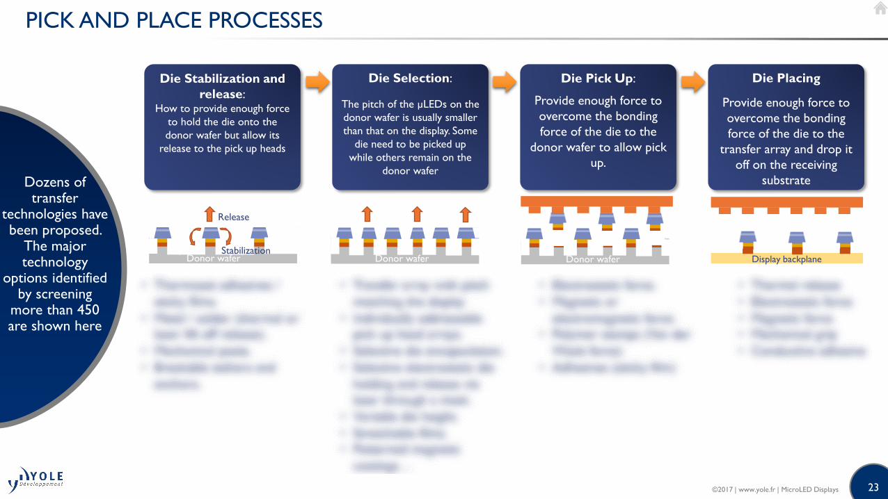
PICK AND PLACE PROCESSES
Dozens of transfer
technologies have been proposed.
The major technology
options identified by screening
more than 450 are shown here
©2017 | www.yole.fr | MicroLED Displays
Die Stabilization and
release:How to provide enough force
to hold the die onto the
donor wafer but allow its
release to the pick up heads
Die Selection:
The pitch of the µLEDs on the
donor wafer is usually smaller
than that on the display. Some
die need to be picked up
while others remain on the
donor wafer
Die Pick Up:
Provide enough force to
overcome the bonding
force of the die to the
donor wafer to allow pick
up.
Die Placing
Provide enough force to
overcome the bonding
force of the die to the
transfer array and drop it
off on the receiving
substrate
Stabilization
Release
Donor wafer Donor wafer Donor wafer Display backplane

24
KEY IP HOLDERS AND CONCLUSION
• More than 20 companies have patented massively parallel transfer
processes for µLEDs. Many more processes could be inferred by
combining the different technology bricks described in this section.
• Most are probably just concepts that haven’t yet reached the stage
of prototypes. None has yet been fully validated in volume
production to the exception of the PDMS stamp process
developed by the team of Prof. Rogers at the University of
Illinois and used by startup Semprius for photovoltaic
applications. X-Celeprint is developing and commercializing the
technology for µLEDs and other micro-devices.
• Beside X-Celeprint, the most advanced company in the field of
massively parallel transfer of µLEDs is likely to be Apple via its
acquisition of Luxvue in 2014. We believe their the technology to
be more complex (MEMS vs polymer stamp) but deliver higher
throughputs and be capable of handling smaller size of µLEDs. Both
companies however remains secretive about actual performance of
their technology.
• Another issue not developed in this report is that of the transfer
equipment which must ensure very high positioning accuracy at
both the pick up and drop off steps. Multiple patents describing
transfer tools have been filed by XXX, XXX, XXX etc.
Mass transfer is a cornerstone of µLED display technologies.
Luxvue and X-Celeprint have
solid IP portfolio on the topic.
©2017 | www.yole.fr | MicroLED Displays
Main patent applicants involved in massively
parallel pick and place technology(according to the number of their patent families*)
* A patent family is a set of patents filed in multiple countries by a
common inventor(s) to protect a single invention.
Source:

25
DEFECT MANAGEMENT STRATEGIES
Illustrations: reducing die size to a level where redundancy becomes cost effective, i.e. when decrease in repair cost offsets epiwafer cost increase. The graph
shows our simulation for various applications of the epiwafer cost thresholds and corresponding die size at which redundancy becomes cost effective
For displays with high pixel counts and pixel density,
pixel repair dominates the transfer cost.
Pixel redundancy becomes efficient if die size can be
reduced.
©2017 | www.yole.fr | MicroLED Displays
$XX $XX
$XX$XX
Added e
pi co
stA
dded e
pi co
st
Die sizeDie size
Die sizeDie size

26
OVERVIEW OF EPIWAFER AND TRANSFER COST PER APPLICATION [1]
©2017 | www.yole.fr | MicroLED Displays
[1] cost for transfer and epiwafer only. Doesn’t include: backplane, color conversion, optics, testing …
[2]: assumes XxX cm2 transfer array
[3]: assumes Xx subpixel redundancy: doubles epiwafer cost and the number of transfer cycles but put repair cycles at zero.
Smartwatch
QHD
Smartphone
(Galaxy S7 )
4K Smartphone
(Xperia Z5
Premium)
9” Tablet
(iPAD Pro)
13” Laptop
(MacBook Pro)
FHD
Monitor
4K
Monitor
4K
55" TV
8K
85" TV
Resolution 312 x 390 1440 x 2560 2160 x 3840 1536 x 2048 2560 x 1600 1920 x 1080 3840 x 2160 3840 x 2160 7680 x 4320
PPI 325 577 801 264 277 102 185 80 104
# of transfer
cycles [2]XX XX XX XX XX XX XX XX XX
# of repairs at
100 ppm
defects
37 1,106 2,489 944 1,229 623 2,489 2,489 9,954
Total Transfer
costXX XX XX XX XX XX XX XX XX
Total Epiwafer
costXX XX XX XX XX XX XX XX XX
Total XX XX XX XX XX XX XX XX XX
Total with
redundancy [3]XX XX XX XX XX XX XX XX XX

27
MICROLED SWOT PER APPLICATION
©2017 | www.yole.fr | MicroLED Displays

28
TRADE OFFS FOR THE DESIGN OF A VR HEADSET
©2017 | www.yole.fr | MicroLED Displays
Sony

29
MOCVD REQUIREMENT
• Assuming displays realized with XX x XX µm size µLEDs, about XXx multiwafer (Veeco’s Epik 700 type) or XXX
single-wafer reactors would be needed to supply Apple needs. If the µLED size can be reduced to XX x XX µm, the
numbers drop to XX and XX respectively.
• Note however that those numbers assume a production run rate averaged throughout the year. Higher numbers
(+20~30%) would be needed to absorb the higher run-rates typically experienced in the few the months preceding a
product launch.
Smartwatch market would
put only moderate strain
on the LED supply chain
©2017 | www.yole.fr | MicroLED Displays
XX x XX µm MicroLED Scenario with 2x redundancy
2019 2020 2021 2022 2023 2024 2025
# of 6" epiwafers
# of MOCVD
(12 x 6")
# of 8" Epiwafers
# of MOCVD
(1 x 8")
XX x XX µm MicroLED Scenario with 2x redundancy
2019 2020 2021 2022 2023 2024 2025
# of 6" epiwafers
# of MOCVD
(12 x 6")
# of 8" Epiwafers
# of MOCVD
(1 x 8")
Note: indicates total cumulated # of MOCVD tools

30
RELATED REPORTS
Discover more related reports
within our bundles here.
©2017 | www.yole.fr | MicroLED Displays

ORDER FORM
Performed by
DELIVERY on receipt of payment:
By credit card:Number: |__|__|__|__| |__|__|__|__| |__|__|__|__| |__|__|__|__|
Expiration date: |__|__|/|__|__| Card Verification Value: |__|__|__|
By bank transfer:HSBC - CAE- Le Terminal -2 rue du Charron - 44800 St Herblain FranceBIC code: CCFRFRPP
In EURBank code : 30056 - Branch code : 00955 - Account : 09550003234 IBAN: FR76 3005 6009 5509 5500 0323 439
In USDBank code : 30056 - Branch code : 00955 - Account : 09550003247 IBAN: FR76 3005 6009 5509 5500 0324 797
Return order by: FAX: +33 2 53 55 10 59MAIL: SYSTEM PLUS CONSULTING
21 rue La Nouë Bras de Fer44200 Nantes – France
Contact: EMAIL: [email protected]: +33 2 40 18 09 16
BILLING CONTACT
ABOUT SYSTEM PLUS CONSULTING
Name (Mr/Ms/Dr/Pr):......................................................................................Job Title:......................................................................................Company:......................................................................................Address:......................................................................................City: State:......................................................................................Postcode/Zip:......................................................................................Country:......................................................................................VAT ID Number for EU members: ......................................................................................Tel:......................................................................................Email:.....................................................................................
Date:.......................................................................................Signature:......................................................................................
First Name: ..................................................................Last Name: ...................................................................Email:............................................................................Phone:...........................................................................
SHIP TO PAYMENT
Please process my order for “MicroLED Displays” Reverse Costing Report
Full Reverse Costing report: EUR 6,490*
Annual Subscription (including this report as the first of the year):
System Plus Consulting is specialized in the cost analysis of electronics from semiconductor devices to electronic systems. A complete range of services and costing tools to provide in-depth production cost studies and to estimate the objective selling price of a product is available.
Our services:
TECHNOLOGY ANALYSIS - COSTING SERVICES - COSTING TOOLS - TRAININGS
www.systemplus.fr - [email protected]
o 3 reports EUR 8 400*o 5 reports EUR 12 500*
o 7 reports EUR 16 000*o 10 reports EUR 21 000*o 15 reports EUR 27 500*
*For price in dollars please use the day’s exchange rate *All reports are delivered electronically in pdf format *For French customer, add 20 % for VAT*Our prices are subject to change. Please check our new releases and price changes on www.systemplus.fr. The present document is valid 6 months after its publishing date: February 2017
Ref.: YDLS17003

TERMS AND CONDITIONS OF SALES
1.INTRODUCTIONThe present terms and conditions apply to the offers, sales and deliveries of services managed by System Plus Consultingexcept in the case of a particular written agreement.Buyer must note that placing an order means an agreement without any restriction with these terms and conditions.
2.PRICESPrices of the purchased services are those which are in force on the date the order is placed. Prices are in Euros and workedout without taxes. Consequently, the taxes and possible added costs agreed when the order is placed will be charged onthese initial prices.System Plus Consulting may change its prices whenever the company thinks it necessary. However, the company commitsitself in invoicing at the prices in force on the date the order is placed.
3.REBATES and DISCOUNTSThe quoted prices already include the rebates and discounts that System Plus Consulting could have granted according to thenumber of orders placed by the Buyer, or other specific conditions. No discount is granted in case of early payment.
4.TERMS OF PAYMENTSystem Plus Consulting delivered services are to be paid within 30 days end of month by bank transfer except in the case of aparticular written agreement.If the payment does not reach System Plus Consulting on the deadline, the Buyer has to pay System Plus Consulting a penaltyfor late payment the amount of which is three times the legal interest rate. The legal interest rate is the current one on thedelivery date. This penalty is worked out on the unpaid invoice amount, starting from the invoice deadline. This penalty issent without previous notice.When payment terms are over 30 days end of month, the Buyer has to pay a deposit which amount is 10% of the total
invoice amount when placing his order.
5. OWNERSHIPSystem Plus Consulting remains sole owner of the delivered services until total payment of the invoice.
6.DELIVERIESThe delivery schedule on the purchase order is given for information only and cannot be strictly guaranteed. Consequentlyany reasonable delay in the delivery of services will not allow the buyer to claim for damages or to cancel the order.
7.ENTRUSTED GOODS SHIPMENTThe transport costs and risks are fully born by the Buyer. Should the customer wish to ensure the goods against lost ordamage on the base of their real value, he must imperatively point it out to System Plus Consulting when the shipment takesplace. Without any specific requirement, insurance terms for the return of goods will be the carrier current ones(reimbursement based on good weight instead of the real value).
8.FORCE MAJEURESystem Plus Consulting responsibility will not be involved in non execution or late delivery of one of its duties described inthe current terms and conditions if these are the result of a force majeure case. Therefore, the force majeure includes allexternal event unpredictable and irresistible as defined by the article 1148 of the French Code Civil?
9.CONFIDENTIALITYAs a rule, all information handed by customers to system Plus Consulting are considered as strictly confidential.A non-disclosure agreement can be signed on demand.
10.RESPONSABILITY LIMITATIONThe Buyer is responsible for the use and interpretations he makes of the reports delivered by System Plus Consulting.Consequently, System Plus Consulting responsibility can in no case be called into question for any direct or indirect damage,financial or otherwise, that may result from the use of the results of our analysis or results obtained using one of our costingtools.
11.APPLICABLE LAWAny dispute that may arise about the interpretation or execution of the current terms and conditions shall be resolvedapplying the French law.It the dispute cannot be settled out-of-court, the competent Court will be the Tribunal de Commerce de Nantes.
Performed by

32
FIELDS OF EXPERTISE
Yole Développement’s 30 analysts operate in the following areas
MEMS & Sensors
LED
Compound
Semi.
Imaging
Photonics
MedTech
Manufacturing
Advanced
Packaging
Batteries / Energy Management
Power Electronics
Displays
RF
Devices &
Techno.
Advanced
Substrates©2017 | www.yole.fr | MicroLED Displays

33
4 BUSINESS MODELS
o Consulting and Analysis
• Market data & research, marketing analysis
• Technology analysis
• Strategy consulting
• Reverse engineering & costing
• Patent analysis
www.yole.fr
o Reports
• Market & technology reports
• Patent Investigation and patent infringement risk analysis
• Teardowns & reverse costing analysis
• Cost simulation tool
www.i-Micronews.com/reports
o Financial services
• M&A (buying and selling)
• Due diligence
• Fundraising
• Maturation of companies
• IP portfolio management & optimization
www.yolefinance.com
www.bmorpho.com
o Media
• i-Micronews.com website
• @Micronews e-newsletter
• Communication & webcast services
• Events
www.i-Micronews.com
©2017 | www.yole.fr | MicroLED Displays
34
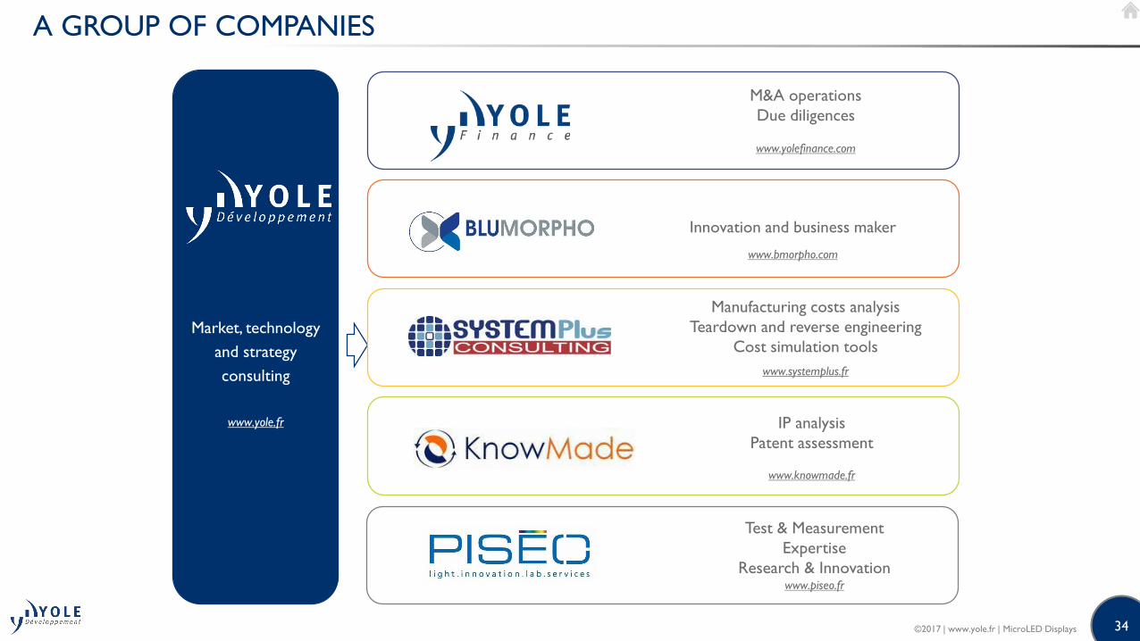
A GROUP OF COMPANIES
Market, technology
and strategy
consulting
www.yole.fr
M&A operations
Due diligences
www.yolefinance.com
Manufacturing costs analysis
Teardown and reverse engineering
Cost simulation tools
www.systemplus.fr
IP analysis
Patent assessment
www.knowmade.fr
Innovation and business maker
www.bmorpho.com
Test & Measurement
Expertise
Research & Innovationwww.piseo.fr
©2017 | www.yole.fr | MicroLED Displays

35
OUR 2017 REPORTS PLANNING (1/2)
MARKET AND TECHNOLOGY REPORTS by Yole Développement
o MEMS & SENSORS
− Fingerprint Sensor Applications and Technologies - Consumer Market Focus 2017
− MEMS Microphones, Speakers and Audio Solutions 2017
− Status of the MEMS Industry 2017
− MEMS & Sensors for Automotive 2017
− High End Inertial Sensors for Defense and Industrial Applications 2017
− Sensor Modules for Smart Building 2017
− Sensing and Display for AR/VR/MR 2017 (Vol 1)
− MEMS Packaging 2017
− Magnetic Sensors Market and Technologies 2017**
− Microspectrometers Markets and Applications 2017**
o RF DEVICES AND TECHNOLOGIES
− RF Components and Modules for Cellphones 2017
− Advanced RF SiP for Cellphones 2017
− 5G and Beyond (Vol 1): Impact on RF Industry, from Infrastructure to Terminals 2017
− 5G and Beyond (Vol 2): RF Materials Platform, from Infrastructure to Terminals 2017
− RF Technologies for Automotive Applications 2017
− GaN and Si LDMOS Market and Technology Trends for RF Power 2017
o IMAGING & OPTOELECTRONICS
− 3D Imaging & Sensing 2017
− Status of the CMOS Image Sensor Industry 2017
− Camera Module for Consumer and Automotive Applications 2017
− Uncooled Infrared Imaging Technology & Market Trends 2017
− Active Imaging and Lidars 2017 (vol 1)
o MEDTECH
− Status of the Microfluidics Industry 2017
− Solid State Medical Imaging 2017
− Sensors for HomeCare 2017
− Sensors for Medical Robotics 2017
− Organs-on-a Chip 2017
o ADVANCED PACKAGING
− Advanced Substrates Overview 2017
− Status of the Advanced Packaging Industry 2017
− Fan Out Packaging: Market & Technology Trends 2017
− 3D Business Update: Market & Technology Trends 2017
− Advanced QFN: Market & Technology Trends 2017**
− Inspection and Metrology for Advanced Packaging Platform 2017**
− Advanced Packaging for Memories 2017
− Embedded Die Packaging: Technologies and Markets Trends 2017
o MANUFACTURING
− Glass Substrate Manufacturing 2017
− Equipment & Materials for Fan Out Technology 2017
− Equipment & Materials for 3D T(X)V Technology 2017
− Emerging Non Volatile Memories 2017
** To be confirmed
©2017 | www.yole.fr | MicroLED Displays

36
OUR 2017 REPORTS PLANNING (2/2)
o POWER ELECTRONICS
− Status of Power Electronics Industry 2017
− Power Mosfets Market and Technology Trends 2017
− IGBT Market and Technology Trends 2017
− Power Packaging Market and Technology Trends 2017
− Power SiC 2017: Materials, Devices, and Applications
− Power GaN 2017: Materials, Devices, and Applications
− Materials Market Opportunities for Cellphone Thermal Management (Battery
Cooling, Fast Charging, Data Processing, Battery Cooling, etc.) 2017
− Gate Driver Market and Technology Trends in Power Electronics 2017
− Power Management ICs Market Quarterly Update 2017
− Power Electronics for Electrical Aircraft, Rail and Buses 2017
− Thermal Management for LED and Power 2017
o BATTERY AND ENERGY MANAGEMENT
− Status of Battery Industry for Stationary, Automotive and Consumer Applications 2017
o COMPOUND SEMICONDUCTORS
− Power SiC 2017: Materials, Devices, and Applications
− Power GaN 2017: Materials, Devices, and Applications
− GaN and Si LDMOS Market and Technology Trends for RF Power 2017
− Bulk GaN Technology Status and Market Expectations (Power, LED, Lasers) 2017
o DISPLAYS
− Microdisplays and MicroLEDs 2017
− Display for Augmented Reality, Virtual Reality and Mixed Reality 2017
− QD for Display Applications 2017
− Phosphors & Quantum Dots 2017 - LED Downconverters for Lighting & Displays
− Emerging Display Technologies 2017**
o LED
− UV LEDs 2017 - Technology, Manufacturing and Application Trends
− Agricultural Lighting 2017 - Technology, Industry and Market Trends
− Automotive Lighting 2017 - Technology, Industry and Market Trends
− Active Imaging and Lidar 2017 (Vol 2) - IR Lighting**
− LED Lighting Module 2017 - Technology, Industry and Market Trends
− IR LEDs 2017 - Technology, Manufacturing and Application Trends
− Phosphors & Quantum Dots 2017 - LED Downconverters for Lighting & Displays
− CSP LED Module 2017
− LED Packaging 2017
PATENT ANALYSIS by Knowmade
− 3D Monolithic Memory: Patent Landscape Analysis
− Microfluidic Diagnostic: Patent Landscape Analysis
− GaN Technology: Top-100 IP profiles**
− Uncooled Infrared Imaging: Patent Landscape Analysis**
− MEMS Microphone: Patent Landscape Analysis**
− MEMS Microphone: Knowles' Patent Portfolio Analysis**
− MicroLEDs: Patent Landscape Analysis**
− Microbolometer: Patents used in products**
− Micropumps: Patent Landscape Analysis**
− Flexible batteries: Patent Landscape Analysis**
TEARDOWN & REVERSE COSTING by System Plus Consulting
More than 60 teardowns and reverse costing analysis and cost simulation tools to be published in
2017.
** To be confirmed
©2017 | www.yole.fr | MicroLED Displays

37
OUR 2016 PUBLISHED REPORTS LIST
MARKET AND TECHNOLOGY REPORTS by Yole Développement
o MEMS & SENSORS
− Gas Sensors Technology and Market 2016
− Status of the MEMs Industry 2016
− Sensors for Cellphones and Tablets 2016
− Market and Technology Trends of Inkjet Printheads 2016
− Sensors for Biometry and Recognition 2016
− Silicon Photonics 2016
o IMAGING & OPTOELECTRONICS
− Status of the CMOS Image Sensor Industry 2016
− Uncooled Infrared Imaging Technology & Market Trends 2016
− Imaging Technologies for Automotive 2016
− Sensors for Drones & Robots: Market Opportunities and Technology Evolution 2016
o MEDTECH
− BioMEMS 2016
− Point of Care Testing 2016: Application of Microfluidic Technologies
o ADVANCED PACKAGING
− Embedded Die Packaging: Technology and Market Trends 2017
− 2.5D & 3D IC TSV Interconnect for Advanced Packaging: Business Update 2016
− Fan-Out: Technologies and Market Trends 2016
− Fan-In Packaging: Business update 2016
− Status and Prospects for the Advanced Packaging Industry in China 2016
o MANUFACTURING
− Thin Wafer Processing and Dicing Equipment Market 2016
− Emerging Non Volatile Memories 2016
o COMPOUND SEMICONDUCTORS
− Power GaN 2016: Epitaxy and Devices, Applications and Technology Trends
− GaN RF Devices Market: Applications, Players, Technology and substrates 2016
− Sapphire Applications & Market 2016: from LED to Consumer Electronics
− Power SiC 2016: Materials, Devices, Modules, and Applications
o LED
− UV LED Technology, Manufacturing and Applications Trends 2016
− OLED for Lighting 2016 – Technology, Industry and Market Trends
− Automotive Lighting: Technology, Industry and Market Trends 2016
− Thermal Management Technology and Market Perspectives in Power Electronics and
LEDs 2017
− Organic Thin Film Transistor 2016: Flexible Displays and Other Applications
− Sapphire Applications & Market 2016: from LED to Consumer Electronics
− LED Packaging 2017: Market, Technology and Industry Landscape
o POWER ELECTRONICS
− Power Electronics for EV/HEV 2016: Market, Innovations and Trends
− Status of Power Electronics Industry 2016
− Passive Components Technologies and Market Trends for Power Electronics 2016
− Power SiC 2016: Materials, Devices, Modules, and Applications
− Power GaN 2016: Epitaxy and Devices, Applications, and Technology Trends
− Inverter Technologies Trends & Market Expectations 2016
− Opportunities for Power Electronics in Renewable Electricity Generation 2016
− Thermal Management Technology and Market Perspectives in Power Electronics and
LEDs 2017
− GaN RF Devices Market: Applications, Players, Technology and substrates 2016
o BATTERY AND ENERGY MANAGEMENT
− Beyond Li-ion Batteries: Present and Future Li-ion Technology Challengers 2016
− Stationary Storage and Automotive Li-ion Battery Packs 2016
− Opportunities for Power Electronics in Renewable Electricity Generation 2016©2017 | www.yole.fr | MicroLED Displays

38
CONTACT INFORMATION
Follow us on
o CONSULTING AND SPECIFIC ANALYSIS
• North America: Steve LaFerriere, Director of Northern America Business DevelopmentEmail: [email protected] – +1 31 06 008 267
• Japan & Rest of Asia: Takashi Onozawa, General Manager, Asia Business DevelopmentEmail: [email protected] - +81 3 4405 9204
• Greater China: Mavis Wang, Director of Greater China Business DevelopmentEmail: [email protected] - +886 979 336 809
• RoW: Jean-Christophe Eloy, CEO & President, Yole DéveloppementEmail [email protected] - +33 4 72 83 01 80
o REPORT BUSINESS
• North America: Steve LaFerriere, Director of Northern America Business DevelopmentEmail: [email protected] – +1 31 06 008 267
• Europe: Lizzie Levenez, EMEA Business Development ManagerEmail: [email protected] - +49 15 123 544 182
• Rest of Asia: Takashi Onozawa, General Manager, Asia Business DevelopmentEmail: [email protected] - +81 3 4405 9204
• Japan & Asia: Miho Othake, Account ManagerEmail: [email protected] - +81 3 4405 9204
• Greater China: Mavis Wang, Director of Greater China Business DevelopmentEmail: [email protected] - +886 979 336 809
o FINANCIAL SERVICES
• Jean-Christophe Eloy, CEO & PresidentEmail: [email protected] - +33 4 72 83 01 80
o GENERAL
• Email: [email protected] - +33 4 72 83 01 80
©2017 | www.yole.fr | MicroLED Displays