formation of holographic memory for defect tolerance in optically reconfigurable gate arrays
TRANSCRIPT

Formation of holographic memory for defect tolerancein optically reconfigurable gate arrays
Akifumi Ogiwara,1,* Minoru Watanabe,2 Takayuki Mabuchi,2 and Fuminori Kobayashi3
1Department of Electronic Engineering, Kobe City College of Technology, 8-3 Gakuen-higashi,Nishiku, Kobe 651-2194, Japan
2Faculty of Engineering, Department of Electrical and Electronic Engineering,Shizuoka University, 3-5-1 Johoku, Hamamatsu, 432-8561, Japan
3Department of Systems Design and Informatics, Kyushu Institute of Technology,680-4 Kawazu, Iizuka, 820-8502, Japan
*Corresponding author: ogiwara@kobe‑kosen.ac.jp
Received 27 April 2010; revised 1 July 2010; accepted 2 July 2010;posted 2 July 2010 (Doc. ID 127284); published 28 July 2010
Holographic polymer-dispersed liquid-crystal (HPDLC) memory using liquid-crystal composites isproposed for new optical information processing. Formation of HPDLC memory using a photomask isdiscussed for parallel programmability to realize fast reconfiguration of optically reconfigurable gatearrays (ORGAs). The defect tolerance of HPDLC memory is investigated to clarify the defect limitationof holographic configurations using ORGAs. Experimental results show that the noise ratio less than 15%applied to HPDLC memory rarely affects its diffraction pattern or a reconfiguration context. © 2010Optical Society of AmericaOCIS codes: 090.2900, 160.3710, 160.5470.
1. Introduction
In recent years, holographic gratings have grown inapplications related to light controlling in optical sys-tems [1–5]. A useful approach for holographic gratingis to employ a liquid-crystal (LC) phase, which canconsider the change in birefringence induced by anelectric field as the refractive-index modulation inthe device. Such a device has been realized using apolymer-dispersed liquid crystal (PDLC), consistingof LC droplets embedded in a polymer matrix. If aholographic optical system with a laser source isapplied to the PDLC systems, fine periodic struc-tures produced by cured-polymer and separatedLC phases, that is, holographic PDLC (HPDLC) grat-ings, can be realized by one-time writing of laser ex-posure. The fabrication processes of HPDLC gratingshave been studied to obtain attractive features, suchas high diffraction efficiencies and superior electro-
optical effects [6–19]. Highly birefringent HPDLCgratings are attractive because the LC has a largefield-induced birefringence change, which results inlarge changes in refractive index modulation, andtherefore, diffraction efficiency of the gratings. Sucha highly functionalized optical device plays a funda-mental role in the development of optical and opto-electronic systems for information technologies.
Recently, optically reconfigurable gate arrays(ORGAs), as presented in Fig. 1, have been developedas a multicontext field programmable gate array(FPGA) to realize fast and numerous reconfigurationcontexts using an optical information processingtechnique [20–24]. The ORGAs have shown that theyhave a perfectly parallel programming capabilitywithout using any serial transfer. The performanceof parallel programmable gate array VLSI enablesperfect avoidance of faulty areas; it instead usesthe remaining areas. Moreover, holographic mem-ories are well known to have high defect tolerancebecause each bit of a reconfiguration context can
0003-6935/10/224255-07$15.00/0© 2010 Optical Society of America
1 August 2010 / Vol. 49, No. 22 / APPLIED OPTICS 4255
be generated from the entire holographic memory.For that reason, the damage to some fraction ofthe component rarely affects its diffraction patternor a reconfiguration context. Therefore, ORGAs areextremely robust against the components defects,such as a laser array, a gate array, and a holographicmemory, and is particularly useful for space applica-tions, which require high reliability [25]. Thus, holo-graphic memory to store numerous contexts and toreconstruct them with high quality is an importantpart for the ORGAs system. A useful approach forthe formation of holographic gratings with high effi-ciency and resolution is shown by employing an LCand polymer phase in organic materials [26–28]. Thevolume gratings formed using LC composite materi-als showed high anisotropic diffraction and transpar-ency with little absorption and scattering in thegrating medium, and the recording resolution lessthan 1 μm as high-density holographic memorymaterials are obtained [27]. Thus, the HPDLC grat-ing is expected for the application of a novel holo-graphic memory device.
This paper presents the one-time easily writablevolume holographic memory based on the HPDLCgratings for optically reconfigurable gate arrays,with particular emphasis on its defect tolerance.
2. Defect and Failure Tolerance of ORGA
As explained in Fig. 1, the ORGAs consist of lasersources, an optical holographic memory, and a pro-grammable gate-array VLSI. The defect toleranceof each component is described in the followingsubsections.
A. Laser Array Part
In the ORGAs, several discrete semiconductor lasersor vertical cavity surface-emitting lasers (VCSELs)are used for switching configuration contexts. Afew such laser sources might have defects. However,those defects of laser sources can be avoided easily bynot using defective lasers, and by not using the holo-graphic memory area corresponding to the lasers.Because the ORGAs have numerous reconfigurationcontexts, a slight reduction of the reconfiguration
contexts is negligible. Programmers need only toavoid the defective part in programming reconfigura-tion contexts for a holographic memory. Therefore,given an absolutely correct programming capabilityand a holographic memory that never generates afailed configuration context, the defect tolerance oflaser sources is nearly perfect. For that reason, inORGAs, a laser array can include some defectivelasers.
B. ORGA-VLSI Part
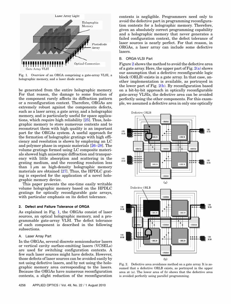
Figure 2 shows themethod to avoid the defective areaof a gate array. Here, the upper part of Fig. 2(a) showsour assumption that a defective reconfigurable logicblock (ORLB) exists in a gate array. In that case, an-other implementation is available, as portrayed inthe lower part of Fig. 2(b). By reconfiguration basedon a bit-by-bit approach in optically reconfigurablegate-array VLSIs, the defective area can be avoidedperfectly using the other components. For this exam-ple, we assumed a defective area in only one optically
Fig. 1. Overview of an ORGA comprising a gate-array VLSI, aholographic memory, and a laser diode array.
Fig. 2. Defective area avoidance method on a gate array. It is as-sumed that a defective ORLB exists, as portrayed in the upperarea at (a). The lower area of (b) shows that the defective areais avoided perfectly using parallel programming.
4256 APPLIED OPTICS / Vol. 49, No. 22 / 1 August 2010

reconfigurable logic block. However, a similar avoid-ance method can be adopted for the other cells, suchas optically reconfigurable switchingmatrices and re-configurable I/O blocks. Therefore, it is confirmedthat the architecture of an ORGA-VLSI part has ahigh defect tolerance.
C. Holographic Memory Part
High defect tolerance is necessary only for theholographic memory part to avoid the defective com-ponents of a laser array andagate-arrayVLSI. There-fore, as described previously, the defect tolerances ofthe laser part and an ORGA-VLSI part depend onthe defect tolerance of the holographic memory part.Generation of failed configuration contexts in the ho-lographicmemory is considered to be serious damage.However, holographic memories are well known tohave a high defect tolerance because each bit of a re-configurationcontextcanbegenerated fromtheentireholographic memory, and damage of some fractionrarelyaffects its diffractionpatternor reconfigurationcontext. Even if a holographicmemorywere to includeasmall defect area, itwouldbeable togenerate correctconfiguration contexts. Thus, the ORGA architectureincluding a holographic memory part is considered tobe highly defect tolerant. However, if almost all of theholographic memory is damaged, the component can-not be used. Therefore, the following experiments areconducted to clarify the defect limitation of the newvolume holographic memory using LC compositesfor holographic configurations.
3. Experimental Procedure
A. Sample Preparation
The holographic memory was formed based on thefabrication process of an HPDLC grating [27]. TheLC composite materials, consisting of mixed pre-polymers (Kyoeisha Chem.), 2-hydroxy-3-phenoxypropyl acrylate, 2-hydroxyethyl methacrylate, anddimethylol tricyclo decane diacrylate with LCmateri-als, were used for the formation of holographic mem-ory. Themixture ratios of the prepolymers were 80, 5,and 15 wt: %, and an LC material (Merck BL024)was added to the aforementioned prepolymer mix-ture at 25 wt: % in the fraction of all ingredients.The xanthene dye (dibromofluoresceine) and N-phenylglycine were introduced as the initiator andcoinitiator, respectively. Then, the mixture of theLCmaterialandprepolymerswas injectedandpouredinto the 10 μm air gap fabricated by two glass plateswith dimensions of 25 mm × 20 mm × 1 mm, wheregap lengthwas preciselymeasured by interferometry.
B. Optical Setup for Device Fabrication
Figure 3 shows the optical setup for the formation ofoptical gratings. Interferometric exposure using agreen laser ðNd:YVO4; λ ¼ 532 nmÞ induces spatiallyperiodic modulation of refractive index at the gratingspacing of 1 μm by the laser beam angle crossed at30° on the samples [26]. Based on the result obtainedin a previous paper [26], the temperature condition
in device fabrication was adjusted at 50 °C usingthe temperature controller with a Peltier elementin this setup. The laser source for photo polymeriza-tion was collimated and linearly polarized perpendi-cularly to the grating vector, and the intensity on thesamples was fixed at 5 mW=cm2. Note that the polar-ization directions parallel and perpendicular to thegrating vector are presently called P and S polariza-tions, respectively.
Aphotomaskwas fabricated by electron beam litho-graphy using a deposited layer of 70 nm of Cr/CrO ona glass plate (Clean Surface Corp.). Figure 4 showsthe configuration of the photomask pattern, consist-ing of arrangements (20 × 17) of circles with adiameter of 20 μm and a distance of 90 μm. The loca-tion of circles corresponds to the photodiode arrange-ments designed in theVLSI chip. The configuration ofthe photomask pattern is originally designed basedon the number and location of circles, including thereconfiguration contexts. The designed photomaskpattern was used to record the information of the re-configuration context as a grating structure by locat-ing 100 mm from the sample in the laserinterferometer, as shown in Fig. 3.
C. Microscopic Observation Methods
Polarizing microscopy was used for the microscopicobservation of the resultant devices. The anisotropyof the materials forming the gratings was observedby polarizing microscopy (Olympus CX31-P) withan objective lens of 100× and a numerical aperture
Fig. 3. Optical setup for fabricating HPDLC memory using alaser interferometer with a photomask.
Fig. 4. Mask pattern consisting of arrangements of circles withdiameter of 20 μm and pitch of 90 μm.
1 August 2010 / Vol. 49, No. 22 / APPLIED OPTICS 4257

(NA) of 0.80. The objective lens for maximum magni-fication (100×), having a long working distance of1:2 mm, was prepared to focus an image clearly onthe grating structure in the HPDLC memory formedbetween two glass plates. The HPDLC memorywas placed between the polarizer and the analyzerarranged under crossed Nicole conditions, andthen the grating structure was observed at severalmagnifications.
D. Configuration System
Figure 5(a) shows a block diagram of the experimen-tal system. The configuration system comprises a la-ser source, an HPDLC memory, and an ORGA-VLSI.A green laser (torus 532; 300 mW, Laser Quantum)with the same wavelength at device fabrication wasused as the laser source to reconstruct a contextpattern. The laser beam of 1:7 mm diameter was ex-panded five times to 8:5 mm by two lenses with 50and 250 mm focal lengths, and the expanded beamwas incident to the HPDLC memory. Figure 5(b)shows a photograph of three-dimensional alignmentof the HPDLC memory and the ORGA-VLSI. TheHPDLC memory, recorded using a photomask de-signed for an AND circuit, was placed 100 mm infront of the ORGA-VLSI. The context for the ANDcircuit was reconstructed by the expanded laserbeam illuminated diagonally at an angle of 30° onthe HPDLC memory, and it was written to theORGA-VLSI for configuration generation. Both theHPDLC memory and the ORGA-VLSI were placedon xyz-3-stages with 0:5 μm resolution for each direc-tion. The positioning adjustments of the HPDLC and
ORGA-VLSI could be executed by frequently execut-ing configuration procedures and by monitoring thecircuit executions of the configured gate array on theORGA-VLSI.
The ORGA-VLSI was fabricated using a comple-mentary metal-oxide-semiconductor process chip of4:9 mm × 4:9 mm, consisting of three-metal layersof 0:35 μm. The ORGA-VLSI chip has four logicblocks, five switching matrices, 12 I/O bits, and 68gates. The 340 photodiodes having a size of 25:5 μm ×25:5 μm and a distance of 90 μm was fabricated inthe chip by an arrangement of 20 × 17. Althoughthe basic part of the VLSI chip is based on the typicalFPGAs, each programming element of all blocks ofthe ORGA-VLSI has connection to an optical recon-figuration circuit to detect an optical configurationcontext. Moreover, the logic block consists of afour-input-one-output lookup table and a delay flip-flop with a reset function. These functions are opti-cally reconfigurable using 40 optical reconfigurationcircuits. Similarly, switching matrices can be recon-figured optically through 12–24 optical connections,and each I/O block is also controlled through nine op-tical connections. Thus, the VLSI part can achieve aperfectly parallel configuration.
4. Results and Discussion
A. Formation of Holographic Structure Using a Photomask
As shown in Fig. 4, the basic configuration of a maskpattern depends on the number and location of cir-cles including reconfiguration contexts. Figure 6shows a part of the holographic structure fabricatedusing a photomask pattern by the arrangements(20 × 17) of a circle with a diameter of 20 μm andpitch of 90 μm. The image is observed in the crossedNicole condition using a polarizing microscope whenthe grating vectors are placed at 45° with respect tothe polarizer [28]. The bright spots in Fig. 6(a) corre-spond to the fringe pattern written by the interfer-ence of laser light as the object beam outgoingthrough a circle of 20 μm diameter formed in thephotomask and collimated laser light as the refer-ence beam incident to the sample at 30°. The clearfringe pattern is observed by the effect of polarizationmodulation in LC composite gratings at the magni-fied image in Fig. 6(b), and the grating spacing is es-timated as 1 μmdesigned by the laser interferometerin Fig. 3. The bright regions of the fringes are re-garded as LC-rich layers because the transmittedlight intensity from the analyzer is increased bythe birefringence of LC molecules in those LC-richlayers [28].
B. Holographic Memory Generation
As shown in Fig. 5, the configuration system com-prises a laser source, a HPDLC memory, and theORGA-VLSIs to detect an optical configurationcontext. Figure 7(a) shows a photomask patternfor an AND circuit consisting of 10 circles. TheHPDLC memory is fabricated using the photomask
Fig. 5. Optical system for the configuration generation by recon-struction using HPDLC memory: (a) block diagram of the experi-mental system and (b) alignment of the HPDLC memory placed infront of the ORGA-VLSI.
4258 APPLIED OPTICS / Vol. 49, No. 22 / 1 August 2010

to demonstrate the optical reconfiguration for theAND circuit. Figure 7(b) shows the reconstructed im-age for the AND circuit by green laser irradiation.White and dark points signify binary states H andL in the image, respectively. The reconstructed inten-sity from theHPDLCmemory is incident to the photo-diode arrays inORGA-VLSIplaced100 mmbehind it.A configuration procedure was confirmed using theoptical reconfiguration system, and the configurationperiod was measured as 9:375 μs, as shown in Fig. 8.Here, the configuration period is defined as the sum-mation of a refresh period, a configuration irradiationperiod, and a setup and hold time of flip-flops. Eachconfiguration procedure is executed by charging thejunction capacitance of photodiodes, the operationof which means the refresh period, then by turningone laser on, the operation of which means the con-figuration irradiation period, and finally by rising aconfiguration clock signal, the operation of which in-cludes a setup and hold time of flip-flops. The config-uration clock signal is connected to all configurationflip-flops to keep the state of a programmable gatearray on ORGA-VLSI. The measured reconfigurationperiod was sufficiently shorter than currently avail-able FPGAs. Based on the result, it is consideredthat the HPDLC memory can be applied to theORGAs to realize parallel programmability and fastreconfiguration.
C. Noise-Applied Experiment for FaultTolerance of ORGA
Using the experimental system shown in Fig. 5, im-pulse noise-applied experiments were executed toclarify the defect tolerance of HPDLC memory withthe context of an AND circuit. The impulse noise wasmade by writing the opaque points on a transparentsheet using a printer. Figure 9 shows the impulsenoise sheets applied by the opaque points from 1%to 20%. Here, we define the meaning of the unit
Fig. 6. Images of the holographic structure observed by thepolarization modulation of LC composite gratings in holographicmemory: (a) bright spots corresponding to circles in photomask,and (b) fringe pattern by magnification of bright region in (a).The image is observed at the crossed Nicole condition with polar-izer (P) and analyzer (A) by a polarizing microscope when the grat-ing vectors are placed at 45° with respect to the polarizer (P).
Fig. 7. (a) Context pattern for AND circuit formed in a photo-mask. (b) Context image reconstructed by holographic memorygeneration.
Fig. 8. Implementation results of an AND circuit. The ANDcircuit was configured and could be executed correctly as seenin the downside three signals, which are two input signals andone output signal of the AND circuit, respectively. The configura-tion period was measured as 9:375 μm.
1 August 2010 / Vol. 49, No. 22 / APPLIED OPTICS 4259

(%) of the noise as a filling factor of the opaque points.Such opaque points correspond to certain emulatedimpulse noises. In this experiment, the noise from0% to 20% was applied to the sheets, and they wereoverlapped onto the HPDLC memory material. Thecontrast images of optical configuration contexts re-duced by the ratio of applied impulse noise from (a)0% to (f) 20% are shown in Fig. 10. Then the config-uration experiments were executed to investigate thedefect tolerance of a new dynamic optically reconfi-gurable gate array with HPDLC memory. Figure 11shows the relation between the reconfiguration timeand the ratio of applied impulse noise. The reconfi-guration time in impulse noise at 0% is shown as22 μs, and it is different from the result measuredas 9:375 μs shown in Fig. 8. The difference of recon-figuration time is caused by the decreased transmit-tance of the transparent sheet used in the impulsenoise-applied experiments. The transmittance of im-pulse noise at 0% does not show 100% because theloss of incident light intensity based on the absor-bance and reflectance of the sheet material. Fromthe figure, it is shown that the reconfiguration timekeeps around 50 μs less than the noise ratio of 15%,whereas at a noise ratio of 20%, it increases at 80 μs.The configurations are possible until the noise ratio
reaches 15%. Therefore, these experimental resultsshow that this new optically reconfigurable gatearray with HPDLC memory has high defect toler-ance. Even if a holographic memory were damagedin space, if the damage were less than 15%, the op-tically reconfigurable gate-array system would beable to function correctly.
5. Conclusions
The formation of HPDLC memory using LC compo-sites was discussed for new ORGA architecture. Aphotomask was fabricated by electron beam litho-graphy to design the arrangement of a circle withdiameter of 20 μm and distance of 90 μm. The config-uration of the photomask pattern was originally de-signed based on the number and location of circles forreconfiguration contexts. The designed photomaskpattern was used to record the information of the re-configuration context as a grating structure in the la-ser interferometer. Polarization microscopy clarifiedthe formation of a fringe pattern by the polarizationmodulation of the LC composite in the HPDLCmemory fabricated by the photomask pattern witha reconfiguration context.
Results of experiments described herein demon-strate that, even if a gate-array VLSI and a laserarray were to include defective parts, the perfectlyparallel programmable capability would enable per-fect avoidance of defective areas. The architectureenables fabrication of large-die VLSI chips andwafer-scale integrations using the latest processes,even with a high defective fraction. In this architec-ture, only a defect of a holographic memory part isunacceptable. Therefore, the experiment to clarifythe defect limitation of HPDLC memory was con-ducted. The experimental results have demonstratedthat the HPDLC memory has a high defect toleranceand that impulse noise less than 15% never affectsits configurations. Finally, we conclude that theORGA architecture using the HPDLC memory hashigh defect tolerance. Future optically reconfig-urable gate arrays with volume holographic mem-ory controlling LC orientation will be a type ofnext-generation three-dimensional VLSI chip with
Fig. 9. Photograph of noise sheets of 1%, 5%, 10%, 15%, and 20%fabricated by writing the opaque points on a transparent sheets.
Fig. 10. CCD-captured images of diffraction patterns of an ANDcircuit context against the ratio of applied impulse noise, such as(a) 0%, (b) 1%, (c) 5%, (d) 10%, (e) 15%, and (f) 20%.
Fig. 11. Configuration time against the ratio of applied impulsenoise.
4260 APPLIED OPTICS / Vol. 49, No. 22 / 1 August 2010

an extremely high gate count and a high defecttolerance.
This research was partially supported by theMinistry of Education, Science, Sports and Cultureof Japan (MESSC-JP), Grant-in-Aid for ScientificResearch on Innovative Areas (20200027). The VLSIchip in this study was fabricated in the chip fabrica-tion program of the VLSI Design and Education Cen-ter (VDEC), the University of Tokyo in collaborationwith Rohm Co., Ltd. and Toppan Printing Co., Ltd.
References1. S. Sanyal, P. Bandyopadhyay, and A. Ghosh, “Vector wave
imagery using a birefringent lens,” Opt. Eng. 37, 592–599(1998).
2. J. E. Ford, F. Yu, K. Urquhart, and Y. Fainman, “Polarizationselective computer-generated holograms,” Opt. Lett. 18, 456–458 (1993).
3. U. D. Zeitner, B. Schnabel, E.-B. Kley, and F. Wyrowski,“Polarization multiplexing of diffractive elements with metalstripe grating pixels,” Appl. Opt. 38, 2177–2181 (1999).
4. F. Gori, “Measuring Stokes parameters by means of polariza-tion grating,” Opt. Lett. 24, 584–586 (1999).
5. S. G. Cloutier, “Polarization holography: orthogonal plane-polarized beam configuration with circular vectorial photoin-duced anisotropy,” J. Phys. D 38, 3371–3375 (2005).
6. R. L. Sutherland, V. P. Tondiglia, L. V. Natarajan, T. J.Bunning, and W. W. Adams, “Electrically switchable volumegratings in polymer-dispersed liquid crystals,” Appl. Phys.Lett. 64, 1074–1076 (1994).
7. T. Karasawa and Y. Taketomi, “Effects of materials systemon the polarization behavior of holographic polymer dispersedliquid crystal gratings,” Jpn. J. Appl. Phys. 36, 6388–6392(1997).
8. A. Ogiwara, Y. Kuratomi, T. Karasawa, A. Takimoto, and S.Mizuguchi, “PS polarization converting device for LC projec-tor using holographic polymer-dispersed LC films,” SID Symp.Dig. 30, 1124–1127 (1999).
9. K. Kato, T. Hisaki, and M. Date, “Alignment-controlled holo-graphic polymer dispersed liquid crystal for reflective displaydevices,” Jpn. J. Appl. Phys. 38, 805–808 (1999).
10. J. J. Butler andM. S. Malcuit, “Diffraction properties of highlybirefringent liquid-crystal composite gratings,” Opt. Lett. 25,420–422 (2000).
11. T. J. Bunning, L. V. Natarajan, V. P. Tondiglia, and R. L.Sutherland, “Holographic polymer-dispersed liquid crystals(H-PDLCs),” Annu. Rev. Mater. Sci. 30, 83–115 (2000).
12. C. C. Bowley and G. P. Crawford, “Diffusion kinetics of forma-tion of holographic polymer-dispersed liquid crystal displaymaterials,” Appl. Phys. Lett. 76, 2235–2237 (2000).
13. R. L. Sutherland, V. P. Tondiglia, L. V. Natarajan, and T. J.Bunning, “Evolution of anisotropic reflection gratings formedin holographic polymer-dispersed liquid crystals,” Appl. Phys.Lett. 79, 1420–1422 (2001).
14. J. J. Butler, M. S. Malcuit, and M. A. Rodriguez, “Diffractiveproperties of highly birefringent volume gratings: investiga-tion,” J. Opt. Soc. Am. B 19, 183–189 (2002).
15. R. L. Sutherland, “Polarization and switching properties ofholographic polymer-dispersed liquid-crystal gratings. I.Theoretical model,” J. Opt. Soc. Am. B 19, 2995–3003(2002).
16. R. L. Sutherland, L. V. Natarajan, V. P. Tondiglia, S. Chandra,C. K. Shepherd, D. M. Brandelik, and S. A. Siwecki, “Polariza-tionandswitchingproperties ofholographicpolymer-dispersedliquid-crystalgratings. II.Experimental investigations,”J.Opt.Soc. Am. B 19, 3004–3012 (2002).
17. M. E. Holmes andM. S. Malcuit, “Controlling the anisotropy ofholographic polymer-dispersed liquid-crystal gratings,” Phys.Rev. E 65, 066603 (2002).
18. Y. Lu, F. Du, and S. T. Wu, “Polarization switch using thickholographic polymer-dispersed liquid crystal grating,” J. Appl.Phys. 95, 810–815 (2004).
19. R. L. Sutherland, V. P. Tondiglia, L. V. Natarajan, andT. J. Bunning, “Phenomenological model of anisotropic volumehologram formation in liquid-crystal-photopolymer mixtures,”J. Appl. Phys. 96, 951–965 (2004).
20. M. Watanabe and F. Kobayashi, “Dynamic optically re-configurable gate array,” Jpn. J. Appl. Phys. 45, 3510–3515(2006).
21. N. Yamaguchi and M. Watanabe, “Liquid crystal holographicconfigurations for ORGAs,” Appl. Opt. 47, 4692–4700 (2008).
22. D. Seto andM. Watanabe, “A dynamic optically reconfigurablegate array—perfect emulation,” IEEE J. Quantum Electron.44, 493–500 (2008).
23. T. Mabuchi, K. Miyashiro, M. Watanabe, and A. Ogiwara,“Fault tolerance of a dynamic optically reconfigurable gate ar-ray with a one-time writable volume holographic memory,” in2009 52nd IEEE International Midwest Symposium on Cir-cuits andSystems (MWSCAS2009) (IEEE, 2009), pp. 917–920.
24. A. Ogiwara, Y. Ochi, M. Miyake, M. Watanabe, T. Mabuchi,and F. Kobayashi, “Formation of volume holographic memoryusing liquid-crystal composites for optically reconfigurablegate array,” in Proceedings of the 15th Microoptics Conference(Japan Society of Applied Physics, 2009), 194–195.
25. M. Nakajima and M. Watanabe, “Optical buffering techniqueunder a space radiation environment,” Opt. Lett. 34, 3719–3721 (2009).
26. A.Ogiwara,H.Kakiuchida,M.Tazawa,andH.Ono, “Analysisofanisotropic diffraction gratings using holographic polymer-dispersed liquid crystal,” Jpn. J. Appl. Phys. 46, 7341–7346(2007).
27. A. Ogiwara, M. Minato, S. Horiguchi, H. Ono, H. Imai,H. Kakiuchida, and K. Yoshimura, “Diffraction properties ofanisotropic volume gratings formed in polymer-dispersedliquid crystal,” Jpn. J. Appl. Phys. 47, 6688–6694 (2008).
28. A. Ogiwara and T. Hirokari, “Formation of anisotropicdiffraction gratings in a polymer-dispersed liquid crystal bypolarization modulation using a spatial light modulator,”Appl. Opt. 47, 3015–3022 (2008).
1 August 2010 / Vol. 49, No. 22 / APPLIED OPTICS 4261