fm demodulation using a digital radio and ... gc1011 digital receiver chip.....16 host...
TRANSCRIPT
FM DEMODULATION USING A DIGITAL RADIO AND DIGITAL SIGNAL
PROCESSING
By
JAMES MICHAEL SHIMA
A THESIS PRESENTED TO THE GRADUATE SCHOOL
OF THE UNIVERSITY OF FLORIDA IN PARTIAL FULFILLMENT
OF THE REQUIREMENTS FOR THE DEGREE OF
MASTER OF SCIENCE
UNIVERSITY OF FLORIDA
1995

Copyright 1995
by
James Michael Shima

To my mother, Roslyn Szego,
and
To the memory of my grandmother, Evelyn Richmond.

iv
ACKNOWLEDGMENTS
First, I would like to thank Mike Dollard and John Abaunza for their extended
support of my research. Moreover, their guidance and constant tutoring were unilaterally
responsible for the origin of this thesis.
I am also grateful to Dr. Scott Miller, Dr. Jose Principe, and Dr. Michel Lynch for
their support of my research and their help with my thesis. I appreciate their investment
of time to be on my supervisory committee.
Mostly, I must greatly thank and acknowledge my mother and father, Ronald and
Roslyn Szego. Without their unending help in every facet of life, I would not be where I
am today. I also acknowledge and greatly appreciate the financial help of my
grandmother, Mae Shima.

v
TABLE OF CONTENTS
ACKNOWLEDGMENTS ................................................................................................. iv
CHAPTER 1 ........................................................................................................................1
INTRODUCTION................................................................................................................1
1.1 Background Overview ............................................................................................1
1.2 Design Motivation ..................................................................................................2
CHAPTER 2 ........................................................................................................................4
CONVENTIONAL AND COMPLEX ANALOG FM DEMODULATION.......................4
2.1 Frequency Modulation and the FM Equation .........................................................4
2.2 FM Demodulation Using Slope Detection..............................................................6
2.3 Derivation of a Complex FM Signal at Baseband ..................................................8
2.3.1 In-Phase Baseband Component .....................................................................9
2.3.2 Quadrature-Phase Baseband Component.....................................................10
2.4 Analog FM Demodulation of a Complex FM Signal at Baseband .......................11
CHAPTER 3 ......................................................................................................................14
DIGITAL RADIO HARDWARE AND SYSTEM ARCHITECTURE ............................14
3.1 The Single-Channel Digital Radio........................................................................14
3.1.1 Architectural Overview................................................................................14
3.1.2 Major Hardware Components of the Digital Radio .....................................15
High-speed analog-to-digital converter..................................................................15
Gray GC1011 digital receiver chip ........................................................................16
Host processor........................................................................................................17
Digital-to-analog converter ....................................................................................18
3.2 Performance Capabilities of the Digital Radio .....................................................18
3.2.1 Capturing High-Frequency RF Signals with the Digital Radio ...................18
3.2.2 Advantages and Disadvantages of a Digital Radio Architecture .................19
3.3 Overview of the Gray GC1011 Digital Receiver Chip .........................................20
3.3.1 Control Interface ..........................................................................................20
3.3.2 Digital Oscillator and Mixer ........................................................................21
3.3.3 Programmable Low-Pass Filter....................................................................22
3.3.4 Decimate-by-Four Low-Pass Filter..............................................................22
3.3.5 Output Format..............................................................................................23

vi
CHAPTER 4 ......................................................................................................................24
ALGORITHM DEVELOPMENT OF THE DIGITAL FM DEMODULATOR...............24
4.1 Complex Vector Representation ...........................................................................24
4.2 Mathematical Modeling of the Digital FM Demodulator .....................................26
4.2.1 The Polar Discriminator...............................................................................26
4.2.2 Digital Limiter and Phase Angle Approximation ........................................30
Development of a digital limiter ......................................................................31
Development of a phase angle estimate function.............................................33
4.3 Demodulator Algorithm Block Diagram ..............................................................36
CHAPTER 5 ......................................................................................................................38
REALIZATION AND TESTING OF THE DIGITAL FM DEMODULATOR................38
5.1 Implementation Issues...........................................................................................38
5.1.1 FM Signal Bandwidth ..................................................................................38
5.1.2 Complex Sampling ......................................................................................39
5.2 Computer Simulations of the FM Demodulator Algorithm..................................42
5.2.1 Polar Discriminator Simulation ...................................................................43
5.2.2 Phase Angle Estimate Simulation................................................................43
5.2.3 FM Demodulator Algorithm Simulation .....................................................45
Polar discriminator and digital limiter .............................................................46
Phase estimate errors........................................................................................46
Spectral analysis...............................................................................................46
5.3 Realization of the FM Demodulator into DSP Code ............................................48
5.3.1 DSP Computational Overhead.....................................................................48
5.3.2 Quantization Errors and Best-Case SNR .....................................................49
5.4 Testing the FM Demodulator................................................................................50
5.4.1 Digital Radio Software and Testing Setup...................................................50
5.4.2 SNR Measurements .....................................................................................50
CHAPTER 6 ......................................................................................................................53
CONCLUSION AND FUTURE DEVELOPMENT .........................................................53
APPENDIX A....................................................................................................................55
SIMULATION OF THE POLAR DISCRIMINATOR......................................................55
APPENDIX B ....................................................................................................................57
SIMULATION OF THE PHASE ANGLE ESTIMATE FUNCTIONS............................57
APPENDIX C ....................................................................................................................62
SIMULATION OF THE DIGITAL FM DEMODULATOR.............................................62

vii
APPENDIX D....................................................................................................................70
DIGITAL FM DEMODULATOR SOFTWARE LISTING ..............................................70
ADSP-2101 DSP Assembly Code Listing (.DSP) .......................................................70
ADSP-2101 System Builder File (.SYS) .....................................................................78
REFERENCES ..................................................................................................................80
BIOGRAPHICAL SKETCH .............................................................................................81

viii
Abstract of Thesis Presented to the Graduate School
of the University of Florida in Partial Fulfillment of the
Requirements for the Degree of Master of Science
FM DEMODULATION USING A DIGITAL RADIO AND DIGITAL SIGNAL
PROCESSING
By
James Michael Shima
May 1995
Chairman: Scott L. Miller
Major Department: Electrical Engineering
Frequency modulation (FM) and demodulation techniques are well established
and understood when implemented with analog circuits. Recently, state-of-the-art digital
technology allows radio-frequency (RF) signals to be processed in the discrete-time
domain. Modulated RF signals are digitally sampled and then demodulated in real time
using signal processing techniques and a digital signal processor (DSP). A digital board
capable of these tasks is often termed a "digital radio." This paper results from the
availability of a digital radio board. The flexibility of DSP software allows a realization
of different demodulation schemes. The purpose of this paper was to test this new
technology by implementing an FM demodulator using the digital radio. A mathematical
algorithm was developed and translated into DSP software to implement the "digital FM
demodulator." The testing of the digital FM demodulator provided a performance
analysis of the developed algorithm. This paper addresses the detailed background,

ix
development, and testing of a digital FM demodulator as implemented on a digital radio
board.
1
CHAPTER 1
INTRODUCTION
1.1 Background Overview
The breakthrough of high-speed digital signal processors (DSPs) have allowed
traditional analog systems to be realized with today's digital circuit technology. The
advances in computer technology has bred a new realm of discrete-time computing
capability. The decrease in chip area and increase in transistor density of computer CPUs
and DSPs have paved the way for the digital implementation of high-speed real-time
systems.
DSPs have become more popular and cost effective since their inception in the
early 1980s. Therefore, the low-cost DSP is able to take the place of the traditional
microcontroller, unveiling more computing power and versatility at the same cost. The
DSP is considered a "specialized" microprocessor, able to perform signal-processing
tasks efficiently. Since most signal processing stems from the implementation of
discrete-time convolution, DSPs consequently have a very fast multiply-accumulate
architecture. DSPs generally execute one instruction per clock cycle and embody a
Harvard-type architecture.
Analog communication systems have been around for decades. In 1918 Edwin H.
Armstrong invented the superheterodyne receiver circuit, and in 1933 he also invented the
concept of frequency modulation (FM). Until recently, analog receivers and modulation
techniques have been unsurpassed in performance. However, new technologies in digital
communications are utilized in developing high-speed modems, spread-spectrum
2
systems, next-generation cellular radios, and many other digital systems that dwarf their
analog counterparts.
1.2 Design Motivation
Communication systems have traditionally used all analog circuits to recover
modulated radio-frequency (RF) signals. Specifically, FM is a type of analog modulation
that requires an analog phase-locked loop (PLL) or slope detector for demodulation. FM
and other demodulation techniques are well established and understood when
implemented with analog circuits. Recently, state-of-the-art digital technology allows RF
signals to be processed in the discrete-time domain. Hence, modulated RF signals are
digitally sampled and then demodulated in real time using signal processing techniques
and a DSP. A digital board capable of these tasks is often termed a "digital radio". The
digital radio is the digital counterpart of an analog superheterodyne receiver.
The motivation of this paper stems from the availability of a state-of-the-art
digital radio board. Using the power and flexibility of the digital radio board, traditional
analog demodulators can be implemented in DSP software. Since DSP software can be
easily changed, several "digital demodulators" can be written to implement different
demodulation schemes, such as FM, amplitude modulation (AM), or single-sideband
modulation (SSB). The key point of interchangeable software demonstrates the
tremendous flexibility advantage a digital radio solution has over a single-task analog
receiver.
The advent of digital RF technology enables numerous analog systems to be
converted into one digital radio solution through the use of real-time signal processing
software. Many large analog receivers can be replaced with one small digital board.
Custom demodulators are also easily implemented with the digital radio because of its
generic hardware architecture.

3
The digital radio is in its research stage, and it has limited real-time demodulation
abilities. The first step chosen to test this new technology is to implement an FM
demodulator using the digital radio. FM is well established and is the backbone for many
other digital communication schemes, including the frequency-shift keying (FSK)
modulation family and the multilevel signaling modulation schemes. A digital FM
demodulator provides a performance test for the digital radio. These test results provide
some insight for the probable improvements to the digital radio architecture.
Consequently, this paper addresses the background, development, and testing of a digital
FM demodulator as implemented on a digital radio board.

4
CHAPTER 2
CONVENTIONAL AND COMPLEX ANALOG FM DEMODULATION
This chapter reviews FM communications and conventional analog FM
demodulation in order to provide the theoretical framework necessary to develop a digital
FM demodulator.
2.1 Frequency Modulation and the FM Equation
Frequency modulation (FM) is a type of angle-modulated signal. A conventional
angle-modulated signal is defined by the following equation.
X t w t tAngle c( ) cos( ( ) ) = A P c
∆
+ (2.1)
where wc = the carrier frequency (rad/s)
Ac = constant amplitude factor
P(t) = the modulating input signal
m(t) = the original message signal
For FM, the relation of m(t) to P(t) is given by
∫ ∞−⋅=
t
fFM dmDtP ξξ )( )( (2.2)
where Df is a constant measured in radians/volt-seconds.
5
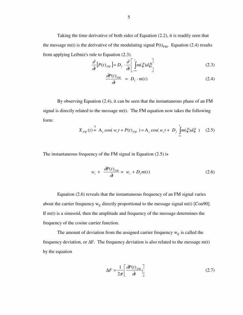
Taking the time derivative of both sides of Equation (2.2), it is readily seen that
the message m(t) is the derivative of the modulating signal P(t)FM. Equation (2.4) results
from applying Leibniz's rule to Equation (2.3).
[ ]
⋅= ∫
∞−
t
fFM dmt
DtPt
ξξ∂
∂
∂
∂)( )( (2.3)
∂
∂
P t
tD m tFM
f
( )( ) = ⋅ (2.4)
By observing Equation (2.4), it can be seen that the instantaneous phase of an FM
signal is directly related to the message m(t). The FM equation now takes the following
form:
) )( cos(A ) )( cos(A = )(
t
-
cc ∫∞
∆
+=+ ξξ dmDtwtPtwtX fcFMcFM (2.5)
The instantaneous frequency of the FM signal in Equation (2.5) is
wP t
tw D m tc
FMc f
+ + = ∂
∂
( )( ) (2.6)
Equation (2.6) reveals that the instantaneous frequency of an FM signal varies
about the carrier frequency wc directly proportional to the message signal m(t) [Cou90].
If m(t) is a sinusoid, then the amplitude and frequency of the message determines the
frequency of the cosine carrier function.
The amount of deviation from the assigned carrier frequency wc is called the
frequency deviation, or ∆F. The frequency deviation is also related to the message m(t)
by the equation
=∆
t
tPF FM
∂
∂
π
)(
2
1 (2.7)

6
Note that ∆F is a non-negative number measured in Hertz. The maximum
frequency deviation of an FM signal, denoted ∆Fmax, is directly proportional to the
amplitude of the input signal. The equation for maximum frequency deviation is given
below.
∆F D m tfmax max ( )= ⋅
1
2π (2.8)
Equation (2.8) makes it obvious that an increase in the message m(t) amplitude
creates an increase in the maximum frequency deviation. The increase in frequency
deviation also increases the bandwidth of the FM signal.
The important relationship established above is that the instantaneous frequency
of an FM signal can be used to directly recover the original message m(t).
Finally, the real FM equation can also be represented as a complex FM signal
through the Euler identity. Recall Equation (2.5)
X t w t P tFM c FM( ) cos( ( ) ) = A c +
which can be written as
[ ] [ ]{ }FMccFM tPtwj
c
twjtPj
cFM eAeeAtX)( )(
Re Re )(+⋅⋅ ⋅=⋅= (2.9)
2.2 FM Demodulation Using Slope Detection
One type of conventional analog FM demodulation is achieved by determining
the instantaneous frequency of an FM generated signal. In theory, an ideal frequency
modulation (FM) detector is a device that produces an output that is proportional to the
instantaneous frequency of the input. A common method of analog FM demodulation is

7
called slope detection. Slope detection is a type of FM-to-AM conversion. Figure 2.1
shows a block diagram of a typical analog FM demodulator using slope detection
[Cou90].
Limiter BPF DifferentiatorEnvelope
Detector
FM inputDemodulated
output
vin(t) vout(t)
Figure 2.1 FM Demodulation for an Analog System Using Slope Detection
The slope detection method revolves around a differentiation operation that
exploits the instantaneous frequency of the FM signal. The FM input signal is first
subjected to a limiter in order to eliminate any amplitude modulation (AM) noise present
in the signal. The output of the limiter is a square wave with constant amplitude. The
square wave is then sent through the bandpass filter (BPF). The BPF has a center
frequency of wc and a bandwidth equal to the bandwidth of the FM signal. The BPF
filters out the square wave harmonics and returns a constant-amplitude sinusoid. The
constant-amplitude FM signal is then differentiated. The differentiation of the cosine
carrier function exploits the instantaneous frequency of the FM signal by the property of
the chain rule. Now, the instantaneous frequency can be thought of as the time-varying
amplitude of the cosine carrier function. The instantaneous frequency is converted to an
AM signal riding on top of the FM carrier function. This is where the principle of FM-to-
AM conversion originates. The last step is to subject the differentiated FM signal to an
envelope detector. The envelope detector extracts the amplitude, or envelope, of the
8
input signal of interest. In the slope detection case, the extracted envelope is the
instantaneous frequency of the FM signal, which contains the original message m(t). In
conclusion, FM demodulation using slope detection recovers the original message m(t) by
determining the instantaneous frequency of the FM signal.
2.3 Derivation of a Complex FM Signal at Baseband
An FM signal at baseband, or zero frequency, is the result of "mixing out" the
carrier frequency from the FM signal, as shown in Figure 2.2. Thus, the carrier frequency
no longer appears in the FM equation. In this paper, the availability of a complex-valued
baseband FM signal is the major advantage in designing the digital FM demodulator. For
this reason, the representation of a complex-valued FM signal at baseband is derived.
Figure 2.2 depicts the generation of a complex baseband FM signal from a conventional
FM signal.
The generation of complex data is the result of mixing the FM signal with a
cosine and sine local oscillator (LO). This process can be derived mathematically by
using the complex version of the FM equation. The mixing process is a simple
multiplication of signals. The cosine mixing term and sine mixing term are multiplied
with the incoming FM signal. For baseband results, both mixers oscillate at the FM
carrier frequency wc. The total mixing operation produces a real (in-phase) and
imaginary (quadrature-phase) baseband component.
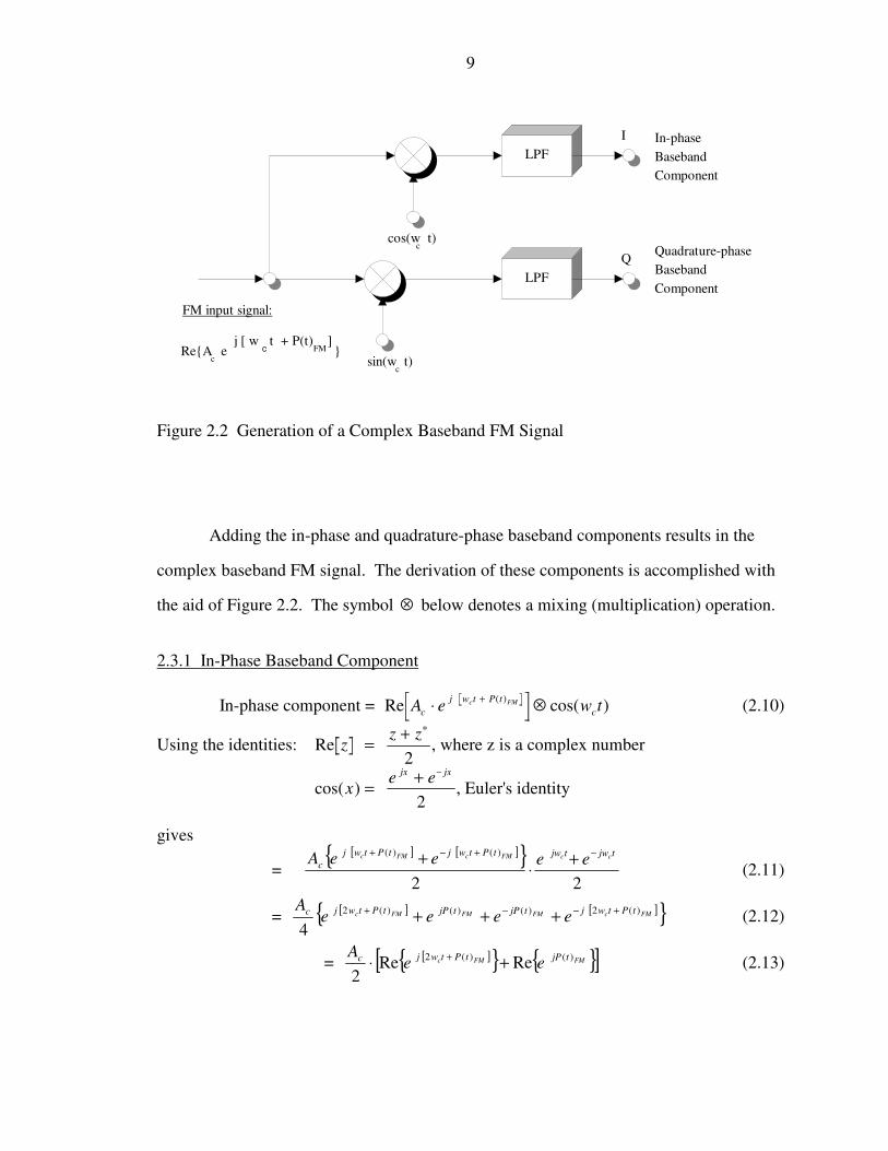
9
LPF
LPF
c
j [ w t + P(t) ]e FM }
FM input signal:
sin(w t)c
cos(w t)c
I
Q
In-phase
Baseband
Component
Quadrature-phase
Baseband
Component
cRe{A
Figure 2.2 Generation of a Complex Baseband FM Signal
Adding the in-phase and quadrature-phase baseband components results in the
complex baseband FM signal. The derivation of these components is accomplished with
the aid of Figure 2.2. The symbol ⊗ below denotes a mixing (multiplication) operation.
2.3.1 In-Phase Baseband Component
In-phase component = Re cos( )( )
A e w tc
j w t P t
cc FM⋅ ⊗
+ (2.10)
Using the identities: Re zz z
=+ ∗
2, where z is a complex number
cos( )xe ejx jx
=+ −
2, Euler's identity
gives
= [ ] [ ]{ }
2
2
)( )( tjwtjwtPtwjtPtwj
cccFMcFMc eeeeA −+−+ +
⋅+
(2.11)
= [ ] [ ]{ }FMcFMFMFMc tPtwjtjPtjPtPtwjc eeee
A )( 2 )()( )( 2
4
+−−+ +++ (2.12)
= [ ]{ } { }[ ]FMFMc tjPtPtwjc ee
A )()( 2 ReRe
2+⋅ +
(2.13)

10
For conventional FM signals, the carrier frequency wc is much greater than
message frequency m(t). The first complex exponential term in Equation (2.13) is the up-
converted term since its carrier frequency has been translated to a frequency of 2wc. The
second complex exponential term in Equation (2.13) is the down-converted term since its
carrier frequency has been translated to zero frequency. Reviewing Figure 2.2 and using
the fact that wc >> wm(t), the low-pass filter extracts the down-converted (baseband) term
and filters out the up-converted term. Thus, the real baseband component of the FM
signal can be represented by the following equation.
In-phase baseband component = A
ec jP t FM
2⋅ Re
( ) (2.14)
2.3.2 Quadrature-Phase Baseband Component
Quadrature-phase component = Re sin( )( )
A e w tc
j w t P t
cc FM⋅ ⊗
+
(2.15)
Using the identities: Im zz z
=− ∗
2
, where z is a complex number
sin( )xe e
j
jx jx
=− −
2, Euler's identity
=
[ ] [ ]{ }2
2
)( )(
j
eeeeA tjwtjwtPtwjtPtwj
cccFMcFMc −+−+
−⋅
− (2.16)
= [ ] [ ]{ }FMcFMFMFMc tPtwjtjPtjPtPtwjc eeee
j
A )( 2 )()( )( 2
4
+−−+ −+− (2.17)
= [ ]{ } { }[ ]FMFMc tjPtPtwjc ee
j
A )( )( 2 ImIm
2−⋅ +
(2.18)
Reviewing Figure 2.2, the low-pass filter extracts the down-converted (baseband)
term in Equation (2.18) and filters out the up-converted term in Equation (2.18). Thus,

11
the imaginary baseband component of the FM signal can be represented by the following
equation.
Quadrature-phase baseband component = jA
ec jP t FM
2⋅ Im
( ) (2.19)
Now, the complex baseband FM signal can be written as the sum of Equations
(2.14) and (2.19), the in-phase and quadrature-phase baseband components.
{ } { }[ ] Im Re 2
)()()( FMFM
baseband
tjPtjPc
FM ejeA
tX +⋅= (2.20)
or,
[ ] [ ]{ } FM
baseband
tjP
FMFM
c
FM etPjtPA
tX)(c
2
A )(sin)(cos
2 )( =+⋅= (2.21)
The design of the digital FM demodulator hinges on Equation (2.21). This
complex baseband FM equation will be referred to during the FM demodulator
development phase. By inspection of Equation (2.21), the complex FM signal at
baseband is represented as a complex exponential function with a varying frequency
directly related to P(t)FM. The complex baseband FM signal can also be demodulated
using standard analog methods. A demonstration of complex baseband FM demodulation
by the slope detection method is presented next.
2.4 Analog FM Demodulation of a Complex FM Signal at Baseband
With the aid of Figure 2.1, the demodulation of the complex baseband FM signal
using the slope detection method is presented. Recall the complex baseband FM equation
from Equation (2.21).
X t eFM
jP t
baseband
FM( )( )
A
c=2

12
The input signal first passes through the limiter circuit. Assume that the limiter
transforms the input signal to a square wave with amplitude Vc. At the output of the
BPF, the FM signal is recovered and takes the form.
X t eFM
jP t FM( )( )
limiter-bpf V c= (2.22)
Following Figure 2.1, the signal next passes through the differentiation block.
After differentiating, the FM signal can be represented by
X t jP t
teFM
FM jP t FM( ) (( )
)( )
lim-bpf -diff V c= ⋅
∂
∂ (2.23)
The last block in Figure 2.1 is the envelope detector. The envelope detector
extracts the magnitude of the signal.
X t jP t
te
P t
tFM
FM jP t FMFM( ) (( )
)( )( )
lim-bpf -diff -ed V Vc c= ⋅ = ⋅
∂
∂
∂
∂ (2.24)
Recall from Equation (2.4), the original message m(t) is the derivative of P(t)FM.
Thus, the demodulated result is
X t D m tFM f( ) ( )demodulated
Vc= ⋅ ⋅ (2.25)
or,
X t m tFM( ) ( )demodulated
C= ⋅ (2.26)
where C is a constant value.

13
Equation (2.26) proves that demodulating a complex analog baseband FM signal
using the slope detection method yields the original message m(t). This conclusion is
used to justify the algorithm development of the digital FM demodulator. Hence, the
theoretical foundation for the digital FM demodulator development has been established
using an analog approach.

14
CHAPTER 3
DIGITAL RADIO HARDWARE AND SYSTEM ARCHITECTURE
This chapter discusses the system architecture and major hardware components on
the digital radio board. Recall, the FM demodulator algorithm design revolves around the
availability of complex-valued baseband digital data from the digital radio hardware.
This demonstrates a classic case of designing software around the capabilities of the
available hardware.
3.1 The Single-Channel Digital Radio
3.1.1 Architectural Overview
The digital radio is a single-channel communications-based receiver. Different
from its analog counterpart, the digital radio consists of all digital components and
performs all signal processing without traditional analog circuitry. The digital radio is
able to process narrowband signals extracted from a digitized wideband RF source
[Gra91]. The architecture of the digital radio board provides a flexible radio-frequency
(RF) receiver that is controlled strictly through software. The receiver has the advantage
of processing RF signals in the digital domain, which allows digital signal processing
(DSP) methods to be employed. This versatile architecture dwarfs the analog receiver in
that one digital radio can be programmed to perform unlimited tasks which are custom to
the user.
The digital radio architecture is a flexible microprocessor-based design centered
around a Gray GC1011 digital receiver chip. The GC1011 chip is responsible for

15
receiving the incoming RF digitized data, down converting it to baseband, lowering the
sampling rate of the data, and piping it to a host processor for computation and
processing. A generic block diagram of a digital radio architecture is shown in Figure 3.1
[Gra91].
High-speed
A/D converter
Gray GC1011
digital receiver
chip
Peripheral interface
Host DSP
Boot software
DAC
RF antenna
input
Analog output
Figure 3.1 Single-Channel Digital Radio Block Diagram
3.1.2 Major Hardware Components of the Digital Radio
The digital radio board is a surface-mount design (SMD) printed-circuit (PC)
board and runs at a clock speed of 50 MHz. The SMD is needed to realize a high-speed
digital board with clock speeds in this range. A general overview of the major
components are described below. These components implement the major blocks shown
in Figure 3.1.
High-speed analog-to-digital converter
The analog-to-digital (A/D) converter used in the digital radio is a high-speed
Analog Devices 100 Msamples/second ECL flash A/D with 8-bit resolution. It is clocked
at 50 MHz, feeding 50 Msamples/second of digital RF data to the GC1011 digital
receiver chip. The flash A/D was necessary to obtain the conversion speeds needed for

16
the GC1011. A small analog circuit is located before the A/D converter to precondition
the incoming RF analog signal and to maintain a stable reference voltage for the A/D.
Gray GC1011 digital receiver chip
The Gray GC1011 digital receiver chip is the heart of the digital radio. It is
responsible for processing the incoming wideband RF digital data and sending the
resultant narrowband output data to the host processor for analysis. The GC1011 receives
its digital RF data from the high-speed A/D converter. The GC1011 can receive 12-bit
input data samples but is constrained to 8-bit input data due to the hardware limitations of
a 12-bit flash A/D at the time of the board construction. The GC1011 is controlled by a
host processor via the peripheral interface. The host processor configures the GC1011 by
writing to control registers onboard the GC1011. There are sixteen 8-bit control registers
that can be accessed through the GC1011's bi-directional data lines. The four address
lines of the GC1011 are used to address the desired control register. Some major
GC1011 functions that the host processor is able to control include the following:
GC1011 tuning frequency, output data decimation rate, output data spectral formatting,
signal gain, and output data format. A functional description of a typical GC1011 tasking
is listed below.
• The digitized RF data are received by the GC1011 and mixed with the tuning
frequency, which effectively down converts the RF signal to baseband.
• The baseband data are decimated via a programmable low-pass filter cascaded
with a decimate-by-four low-pass filter in order to lower the output bandwidth
of the signal.
• Finally, the data are formatted and sent to the host processor. The data
formats include complex or real output data and flipping or offsetting the
output spectrum.

17
Specifically, the major feature exploited from the Gray GC1011 digital receiver
chip is the generation of complex baseband data . This is an important innovation used to
design the digital FM demodulator.
One limitation of the GC1011 is the ability to tune up to a maximum frequency of
half its operating clock rate. Thus, at a 50 MHz clock speed, the digital radio can directly
digitize and tune to RF frequencies from 0 to 25 MHz. The GC1011 is a memory-
mapped peripheral in the host processor's external memory map. The host processor
configures the GC1011 and controls the GC1011 during program execution by
communicating to the command registers [Gra91].
Host processor
The host processor for the digital radio is a one-instruction-per-cycle digital
signal processor (DSP) chip. A fast DSP processor is needed to handle the flow rate of
data sent from the GC1011. The DSP residing on the digital radio board is an Analog
Devices ADSP-2101, 16-bit fixed-point processor running at a 16 MHz clock
(instruction) rate. The ADSP-2101 is a Harvard architecture RISC microprocessor, i.e.,
separate program and data memories and respective memory maps. All peripherals,
including the GC1011, are memory mapped into the ADSP-2101's external data memory
map. The DSP directly retrieves parallel digital data from the GC1011 and is able to send
the processed results to a digital-to-analog converter (DAC) for analog output. The DSP
runs the operating system software and performs all housekeeping and computational
tasks for the digital radio board. On powerup or system reset, the DSP automatically
boots from an onboard EPROM that contains its tasking software [Ana90].
18
Digital-to-analog converter
The back-end digital-to-analog converter (DAC) is a Burr-Brown 12-bit dual
converter. It is used to retrieve the processed digital data from the DSP and convert it to
an analog output. The output sample rate for the DAC is set by the host processor. The
host writes the desired sample time to a hardware timer that is connected to the DAC load
lines. This architecture allows the DAC timer to interrupt the processor when it times
out. This hardware methodology achieves a stable, constant sampling interval that is not
software dependent. In this design, the demodulated FM data was sent from the host
processor to the DAC for analog audio output.
3.2 Performance Capabilities of the Digital Radio
3.2.1 Capturing High-Frequency RF Signals with the Digital Radio
An inherent bottleneck of the digital radio surfaces when targeting very-high
frequency (VHF) and ultra-high frequency (UHF) signals. In order to process VHF and
UHF radio signals, a front-end analog down converter must be used in conjunction with
the digital radio in order to down convert the band of interest into the GC1011's tuning
range. Recall, the GC1011 can only directly tune up to a maximum frequency of 25 MHz
with a 50 MHz clock rate. This specification limits the range of frequencies accessible to
the digital radio board. Specifically, any frequency over 25 MHz cannot be received by
the digital radio without the use of a front-end analog down converter. For this paper,
this was not a problem since the FM modulated signal was generated with a carrier
frequency within the GC1011 tuning range. However, in practical use this problem can
be alleviated by using a standard VHF/UHF receiver as the down converter. The
intermediate frequency (IF) output from the VHF/UHF receiver can be used as the
19
GC1011's tune frequency. The two most common IF frequencies for FM systems are
10.7 MHz and 21.4 MHz. The GC1011 can directly tune up to either of these IF
frequencies. The output IF frequency from the VHF/UHF receiver is just the down-
converted term of the RF signal. Hence, this IF frequency can be used as the RF input to
the digital radio, while the GC1011 tune frequency is set to the VHF/UHF receiver's IF
frequency. Since the GC1011 is constantly tuned up to the IF, the digital radio can now
process any frequency the front-end VHF/UHF receiver can supply.
3.2.2 Advantages and Disadvantages of a Digital Radio Architecture
The digital radio performs signal processing tasks via software. This software is
run by the host DSP processor, which configures the hardware on the board and performs
all computational tasks relevant to the desired signal processing task. Thus, by changing
the DSP software, the digital radio effectively becomes a custom narrowband receiver.
Multiple narrowband demodulators, modems, or communication-based algorithms can be
easily implemented on the digital radio. This exemplifies the digital radio's signal
processing flexibility over the conventional single-task analog receiver.
However, there are a few drawbacks to a digital radio architecture at this phase.
First, it is unable to tune up to VHF or UHF signals without the help of an analog down
converter. Secondly, only narrowband signals can be processed from a wideband RF
input. The processing speed of the DSP and GC1011 limits the computational throughput
of the radio. For these reasons, wideband signal processing is generally not feasible using
the current design of the digital radio architecture.
20
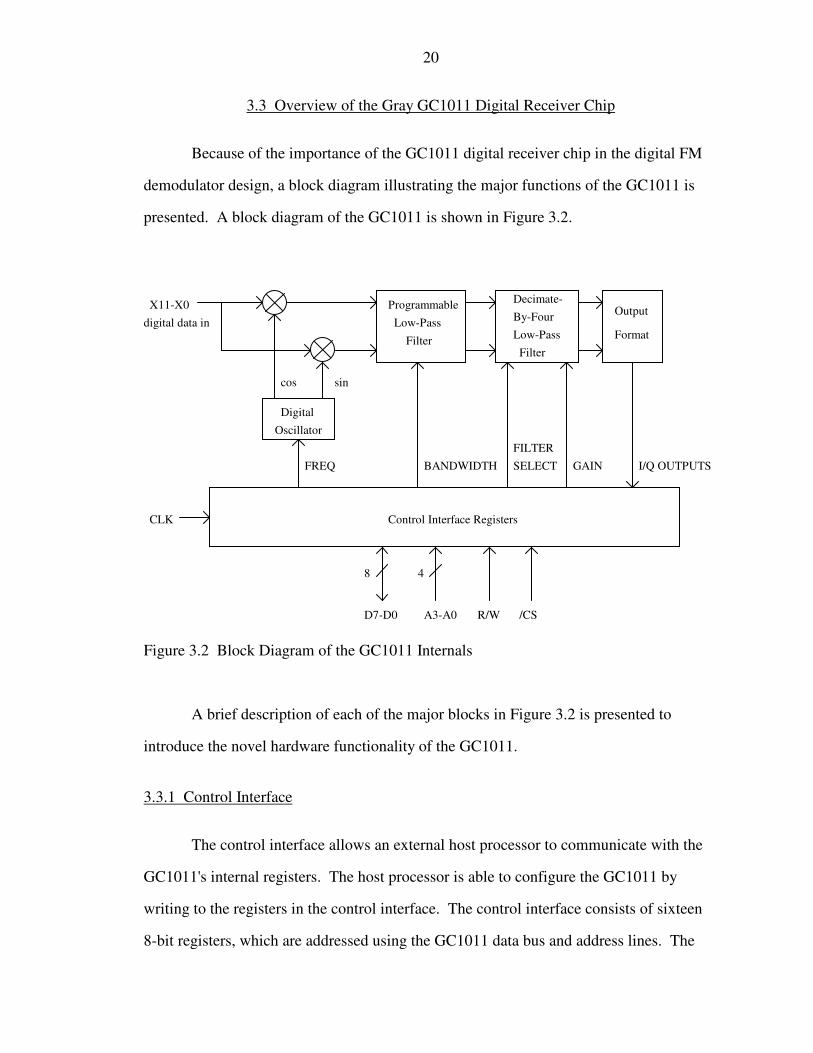
3.3 Overview of the Gray GC1011 Digital Receiver Chip
Because of the importance of the GC1011 digital receiver chip in the digital FM
demodulator design, a block diagram illustrating the major functions of the GC1011 is
presented. A block diagram of the GC1011 is shown in Figure 3.2.
sincos
Digital
Oscillator
digital data in
X11-X0
Control Interface Registers
D7-D0 A3-A0
8 4
R/W /CS
Programmable
Low-Pass
Filter
Decimate-
By-Four
Low-Pass
Filter
Output
Format
FREQ BANDWIDTH
FILTER
SELECT GAIN I/Q OUTPUTS
CLK
Figure 3.2 Block Diagram of the GC1011 Internals
A brief description of each of the major blocks in Figure 3.2 is presented to
introduce the novel hardware functionality of the GC1011.
3.3.1 Control Interface
The control interface allows an external host processor to communicate with the
GC1011's internal registers. The host processor is able to configure the GC1011 by
writing to the registers in the control interface. The control interface consists of sixteen
8-bit registers, which are addressed using the GC1011 data bus and address lines. The

21
GC1011 has eight bi-directional data lines (D7-D0) and four address lines (A3-A0). An
active low chip select (/CS) and read/write pin (R/W) are used to access the chip using
standard memory-mapped peripheral protocols. Also, the resulting 16-bit real (I) and
imaginary (Q) data from the GC1011 is read by the host processor by accessing the
proper data control registers [Gra91]. Because the GC1011 is limited to an 8-bit data bus,
this requires four parallel register reads in order to assemble the 16-bit I and Q output
samples.
3.3.2 Digital Oscillator and Mixer
The digital oscillator is responsible for generating the sine and cosine discrete
sequences which are mixed with the incoming digital data X11-X0. The digital oscillator
consists of a 28-bit frequency register, accumulator, and sine-cosine digital word
generator. The tuning frequency of the digital oscillator is set by loading the frequency
register with the calculated tuning frequency using the below equation [Gra91].
FREQ Desired tuning freq .)
Clock rate=
228 ( (3.1)
where FREQ is the 28-bit frequency register. The FREQ register is loaded by writing a
frequency word from the host processor to the frequency register in the digital oscillator.
The upper 13 bits of the 28-bit FREQ word are used to generate the digital
oscillator's sine and cosine digital sequences. The resulting digital samples are rounded
to 12 bits. Using the 6-dB rule [Cou90], this allows a maximum of 6(12) = 72 dB of
spurious free dynamic range for the oscillator.
The digital mixer simply multiplies the incoming 12-bit samples (X11-X0) with
the 12-bit sine and cosine sequences. The output of the mixer is a digital sequence at zero
frequency. Thus, mixing an input signal with its carrier frequency equal to the digital
22
oscillator's tuning frequency results in a baseband digital sequence. In other words, the
input sequence is centered at zero frequency after passing through the mixer.
3.3.3 Programmable Low-Pass Filter
The output of the mixer is fed into a programmable low-pass filter in order to
isolate the down converted baseband sequence. The filter also decimates the sequence.
In other words, the filter lowers the sample rate of the sequence by a factor of D [Gra91].
The value of D can range from 16 to 16,384. This parameter is configured by writing to
the BANDWIDTH control register [Gra91], which is illustrated in Figure 3.2.
3.3.4 Decimate-by-Four Low-Pass Filter
The decimate-by-four filter is a fixed low-pass finite-impulse-response (FIR)
decimation filter that further decimates the baseband sequence by four after the initial
programmable low-pass filter. The total sample rate reduction is therefore 4D.
Because of the initially high incoming sample rate, the reduction is necessary in
order to process the embedded modulated signal in real time. Because of the possibility
of aliasing, the reduced sample rate must still meet Nyquist's criteria. In other words, the
output sequence from the final decimation filter must still maintain a sample rate at least
two times the maximum frequency in the modulated signal. Obviously, this decimation
parameter depends on the bandwidth of the desired demodulated signal. Control registers
GAIN and FILTER SELECT exist to correct the filter gain and select one of two FIR
decimation filter types. The decimation filter can either have a 3 dB passband with 70 dB
attenuation in the stop band covering 80% of the Nyquist rate, or a 3 dB passband with 50
dB attenuation in the stop band covering 90% of the Nyquist rate [Gra91].
23
3.3.5 Output Format
The output format block receives the resulting samples from the lowpass filter
network. The output samples are rounded to 16 bits, and the output spectrum is
optionally flipped, converted from a complex to a real spectrum, or offset by one-fourth
the Nyquist rate [Gra91]. The control word written to the filter control register governs
the formatting of the output samples. The resulting 16-bit I and Q samples are sent to the
output storage registers for the host to access. Due to the 8-bit data bus, the host must
perform four parallel reads to retrieve one complex sample from the GC1011. Moreover,
the digital radio board has no GC1011 interrupt capability, so the host must "poll" the
GC1011 in software to determine when a new sample is ready. The ramifications of
software polling is a decrease in the DSP real-time processing window. A software
polling loop requires more DSP instructions than an interrupt-service subroutine, causing
the decrease in the real-time processing window. Other important implementation issues
and inherent hardware limitations are discussed in later chapters.

24
CHAPTER 4
ALGORITHM DEVELOPMENT OF THE DIGITAL FM DEMODULATOR
This chapter discusses the development of the digital FM demodulator using the
theoretical and hardware foundations discussed in the previous chapters. In order to
demodulate a digitally-sampled FM signal, a digital method of determining the
instantaneous frequency of the sampled FM signal is needed. Chapter 2 presented the
analog approach of demodulating a complex-valued FM signal at baseband. These
mathematical steps will be transformed into their digital equivalents, creating a digital
FM demodulator. The end result of this chapter is to fabricate a fast digital FM
demodulator able to run on the digital radio's DSP. Therefore, the attributes of the digital
radio board also governs the design strategy for the demodulator.
4.1 Complex Vector Representation
Figure 4.1 displays the complex Cartesian coordinate system and the complex unit
circle |z| =1. From Equation (2.21), the complex equation for an FM signal at baseband, a
complex-valued FM sample can be represented by a vector on the complex unit circle
having an amplitude and a phase angle. A complex sample gives two pieces of
information, a real and imaginary component. The polar form of a complex number z,
where z = x + j y, can be represented by the following equations.
z r e j = ⋅ θ (4.1)
r x y = +2 2 (4.2)
θ y
x= −tan 1 (4.3)

25
Figure 4.1 labels the quadrants in the complex coordinate system the same as the
standard Cartesian rectangular system.
r
Point (x,y)
Re(z)
Im(z)
Quadrant IQuadrant II
Quadrant IVQuadrant III
j
-1
-j
1
Figure 4.1 Complex Coordinate System
The polar form of a complex number, shown in Equation (4.1), can be used to
extract the phase angle of a complex sample. Each incoming complex sample will have a
new amplitude and phase angle. Since FM signals store all of their information in the
phase, this chapter proves that the phase angle is the information required to demodulate
a complex-sampled FM signal.
Successive complex-valued samples can be shown to "rotate" around the complex
unit circle in Figure 4.1. For example, if a sinusoid with a constant frequency is complex
sampled, each consecutive sample can be represented as a vector rotating around the
26
complex unit circle. The degrees of advancement between consecutive samples can be
expressed by the following equation.
∆θ = frequency of signal
sample rate⋅ 3600 (4.4)
Equation (4.4) is used to directly relate the phase difference between two
complex-valued samples. In the previous example, suppose the sinusoid is sampled at a
rate eight times greater than its frequency. Applying Equation (4.4), each vector will
travel (1/8)(360°) = 45° from the previous sample's location. Furthermore, at the Nyquist
sampling rate, or 2fmax, each successive vector will travel 180° from the last vector's
position. The previous finding demonstrates the key result of the sampling theorem
[Str88]. In order for aliasing not to occur in the sampled signal, consecutive vectors
cannot advance more than 180°.
4.2 Mathematical Modeling of the Digital FM Demodulator
4.2.1 The Polar Discriminator
As stated in the above section, the phase angle contains the necessary information
needed to demodulate a complex-sampled FM signal. Chapter 2 presented the
mathematical foundation supporting this method of FM demodulation for complex FM
signals at baseband. Specifically, determining the instantaneous frequency of the FM
signal recovers the original message.
One approach for determining the digital instantaneous frequency of a complex-
sampled FM signal is by using a polar discriminator. A polar discriminator measures the
phase difference between consecutive samples of a complex-sampled FM signal. This
phase difference turns out to be the instantaneous frequency of the sampled FM signal.

27
A polar discriminator operates by taking successive complex-valued samples and
multiplying the new sample by the conjugate of the old sample. Consider two
consecutive complex-valued baseband FM samples with unity magnitude and phase
angles Θ1 and Θ2, respectively. The polar discriminator can be represented
mathematically in polar form by using Equation (2.21).
FM ebaseband
j
1
= θ1 (4.5)
FM ebaseband
j
2
= θ2 (4.6)
e e e ( ) ( ) ( )j j j⋅ − ⋅ ⋅ −⋅ =θ θ θ θ2 1 2 1 (4.7)
Equation (4.7) is the result of the polar discriminator. The polar discriminator
takes two complex-valued samples with different phase angles and returns the phase
difference between the samples. Note that the difference operation in the digital domain
is an approximation of a time differentiation in the analog domain. For discrete-time
systems this differentiation can be represented as a backward-difference equation similar
to the equation below [Str88].
[ ]∂
∂
f t
t Tf nT f n T
( )( ) (( ) ) ≈ − −
11 (4.8)
In Equation (4.8), f(t) is a continuous function, T is the sampling period, and n is a
positive integer. Equation (4.8) reveals that the difference operation in Equation (4.7)
approximates the derivative of the FM phase. Actually, using the concepts of finite-
difference calculus shows that Equation (4.8) is exact for first-order functions.1
Therefore, the polar discriminator in Equation (4.7) calculates the exact phase derivative
for signals with first-order frequency characteristics. A polar discriminator returns the
1From William Hager, "Numerical Analysis Lecture Notes", University of Florida, 1992.
28
exact phase derivative for sinusoids with a constant frequency. Moreover, a sinusoid with
a varying frequency (i.e., an FM signal with a sinusoidal message) causes the polar
discriminator to return an approximation of the phase derivative. This differentiation
error is due to the fact that Equation (4.7) is no longer exact for phase functions greater
than first order. However, if the sampling period T is made sufficiently small, it can be
shown that a nonlinear function exhibits a linear behavior between closely-spaced sample
points [Str88]. Thus, a small sampling period T increases the accuracy of the polar
discriminator for a sinusoidal input with a nonlinear frequency.
Equations (2.4) and (4.7) show that the calculated derivative from the polar
discriminator is equivalent to the instantaneous phase of the sampled FM signal. This
instantaneous phase is synonymous with the instantaneous frequency of an analog FM
signal. Therefore, the phase difference between the two consecutive complex-valued FM
samples is the information needed to demodulate the sampled FM signal. A signal flow
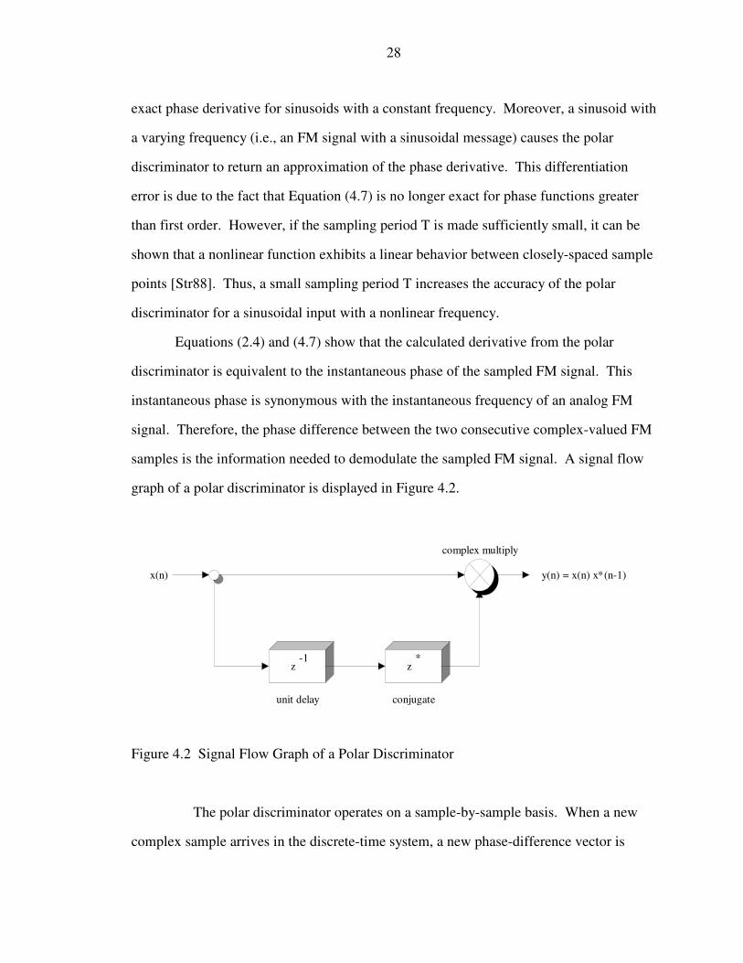
graph of a polar discriminator is displayed in Figure 4.2.
x(n)
z-1
unit delay
z*
y(n) = x(n) x (n-1)*
conjugate
complex multiply
Figure 4.2 Signal Flow Graph of a Polar Discriminator
The polar discriminator operates on a sample-by-sample basis. When a new
complex sample arrives in the discrete-time system, a new phase-difference vector is

29
calculated. Some of the key characteristics of the polar discriminator when operating on
a sampled FM input signal are listed below.
• A sampled sinusoid with a constant frequency (no modulation) results in
vectors residing at the same location on the unit circle. Recall the case of the
sampled sinusoid with a 45° advancement between samples. By Equation
(4.7), the output of the polar discriminator is a vector with a phase angle equal
to 45°. Therefore, subjecting an unmodulated sinusoid to a polar
discriminator produces vectors with a constant phase angle. This constant
phase angle can be computed using Equation (4.4).
• The origin is equivalent to a vector with a phase angle equal to zero. By
definition, a baseband FM signal is centered at zero frequency. Thus,
subjecting a complex-sampled baseband FM signal to a polar discriminator
results in vectors that migrate about the origin. Figure 4.3 displays the origin
as the line Im(z) = 0, Re(z) > 0.
• For a baseband FM signal, the polar discriminator vectors migrate about the
origin according to the frequency deviation of the FM signal. At any point in
time, if the FM signal has a frequency greater than the carrier frequency wc,
then the polar discriminator vector resides in quadrant I or II and has a positive
phase angle. Likewise, if the FM signal has a frequency less than the carrier
frequency wc, then the polar discriminator vector resides in quadrant IV or III
and has a negative phase angle. Figure 4.3 demonstrates this concept for two
vectors residing in quadrants I and IV, respectively.
• The maximum attainable phase angle of a polar discriminator vector depends
on the sampling rate. By the sampling theorem, if an FM signal is sampled at
the Nyquist rate or higher, then the polar discriminator vectors are constrained
to have phase angles less than 180°.
• If a baseband FM signal is oversampled at a rate of four times or greater, then
the polar discriminator vectors are constrained to rotate within quadrants I and
IV. The sampling rate governs the number of degrees the polar discriminator
vectors migrate from the origin. Therefore, using Equation (4.4), a four times
oversampling rate results in vectors deviating a maximum of 90° from the
origin. Thus, increasing the sampling rate decreases the distance (in degrees)
the polar discriminator vectors deviate from the origin.

30
Re(z)
Im(z)j
-1
-j
1
origin
negative phase vector
positive phase vector
Polar discriminator result
Figure 4.3 Vector Diagram of the Polar Discriminator Results
In summary, utilizing a polar discriminator on successive complex-valued
baseband FM samples gives the instantaneous frequency of the sampled FM signal. The
resulting phase angle from the polar discriminator result contains the information in the
original message m(t).
4.2.2 Digital Limiter and Phase Angle Approximation
The difficult step of recovering the message information from a sampled FM
signal is determining the phase angle from the polar discriminator result. The polar
discriminator returns a complex number z = x + j y. The corresponding phase angle of
that complex number is the instantaneous frequency of the sampled FM signal. From
Equation (2.26), this result is exactly the message m(t). Equation (4.3) shows the exact
method of determining the phase angle θ of a complex number. The true phase angle
calculation involves the arctangent function. Consequently, the arctangent is not an
intrinsic function in any DSP or microprocessor instruction set. Furthermore, computing
a true arctangent is complex and too time consuming for most DSP applications. Thus,

31
an estimate of the arctangent which gives an accurate measure of θ is necessary. There
are many methods for approximating the phase angle of a complex number, and one such
method which is geared for speed is developed in this chapter.
Consider again the complex coordinate system in Figure 4.1. Using Equation
(4.3), the phase angles in quadrants I and II are all positive (0 to π radians). The phase
angles in quadrants III and IV can be considered as negative angles (-π to -2π radians). In
fact, the angles in quadrants III and IV are the exact negatives of the angles in quadrants II
and I, respectively. Therefore, an approximation of the phase angle θ only needs to be
derived for quadrants I and II. This approximation can be translated to quadrants III and
IV by a simple negation.
Development of a digital limiter
In FM the amplitude of the signal is assumed to be constant. However, amplitude
modulation (AM) noise and other contributing factors can vary the amplitude of the
resultant vector from the polar discriminator. A varying amplitude will cause errors in
the phase approximator. The phase approximation must be invariant to the amplitude of
the polar discriminator vector. Recall from Chapter 2 that analog FM demodulators, like
the slope detector in Figure 2.1, solve this problem by using a hard limiter to clip the
signal amplitude to a known value.
In the digital mathematical model, it was discovered that a ratio of the real
component and imaginary component always gives a result that is phase dependent and
amplitude independent. These ratios correspond to a range of numbers that are native to
each quadrant. Consider quadrant I shown in Figure 4.1. The real and imaginary
components of a complex number are positive in quadrant I. A ratio that is amplitude
independent is

32
ratioquadrant I = Re(z) - Im(z)
Re(z) + Im(z) (4.9)
Equation (4.9) relates the real and imaginary components to their position in
quadrant I, but the result does not depend on their amplitude. This result still preserves
the phase, but the division operation makes it amplitude invariant. The ratio in Equation
(4.9) returns real numbers in the range [-1,1]. The equation below shows the critical
points returned by the quadrant I ratio.
≠
≠
=
0 Im(z) 0, =Re(z) 1,-
Im(z) =Re(z) ,0
0 =Im(z) 0, Re(z) ,1
Iratio (4.10)
Equation (4.10) reveals that the ratio in Equation (4.9) returns fractional results.
Thus any vector, invariant of its magnitude, residing in quadrant I will return a unique
number that is relative to its phase in quadrant I. This unique number will be a fractional
number in the range [-1,1]. The fractional result is another design characteristic of the
ratio. The demodulator software will run in a fixed-point (fractional) mode on the DSP.
Thus, the ratio already addresses the problem of obtaining fractional numbers for the
calculations on the DSP. Using the same methodology, the ratio for complex numbers
residing in quadrant II is
ratioquadrant II = Re(z) + Im(z)
Im(z) - Re(z) (4.11)
Equation (4.11) also returns fractional numbers within the range [-1,1]. Recall
from Figure 4.1, imaginary components are positive and real components are negative in
quadrant II. Similar to Equation (4.10), the ratio for quadrant II returns the following
critical points.
33
≠
≠
=
0 =Im(z) 0, Re(z) 1,-
Im(z) =Re(z) ,0
0 Im(z) 0, =Re(z) ,1
IIratio (4.12)
Finally, Equations (4.9) and (4.11) can be computed for all values of a complex
number z in each respective quadrant. As shown, these ratios not only give a means to
estimate the phase, but they also perform the same task as a hard limiter. Therefore, the
digital FM demodulator is not subject to AM noise.
Development of a phase angle estimate function
In order to estimate the actual phase angle returned by the ratios in Equations (4.9)
and (4.11), a relationship between these calculated ratios and the true phase angle θ is
needed. Recall, Equations (4.9) and (4.11) return fractional numbers in the range [-1,1].
These resulting numbers have to be converted to the actual phase angles of each complex
number. Since the processing time for the DSP is finite, an approximation of the actual
phase angle is sufficient. There exists many methods for approximating functions.
Several popular methods include: Table look up, Taylor-series approximation, and
polynomial fitting.
Polynomial fitting, or Lagrange interpolation, was chosen as the phase function
approximation technique. This technique allows any continuous function to be "fitted"
with a polynomial derived from actual data points.2 The method can be used to create
low-order polynomials that only need a few multiplies and additions to produce a
sufficiently accurate function estimate. The ratios from Equation (4.9) and (4.11) act as
the inputs to the Lagrange interpolating polynomial. The resultant polynomial is the
phase angle estimate function. In this mathematical model, one interpolating polynomial
2From William Hager, "Numerical Analysis Lecture Notes", University of Florida, 1992.
34
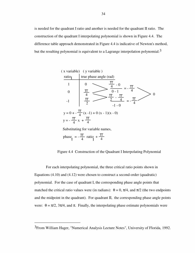
is needed for the quadrant I ratio and another is needed for the quadrant II ratio. The
construction of the quadrant I interpolating polynomial is shown in Figure 4.4. The
difference table approach demonstrated in Figure 4.4 is indicative of Newton's method,
but the resulting polynomial is equivalent to a Lagrange interpolation polynomial.3
ratio true phase angle (rad)
0
-1
1 0 - 0
0 - 1= -
-1 - 0
= -
0
( x variable) ( y variable )
y = 0 + - (x -1) + 0 (x - 1)(x - 0)
y = - x +
Substituting for variable names,
phase = - ratio +
4
2
44
2 4-
4
4
I
4 4
I 4 4I
Figure 4.4 Construction of the Quadrant I Interpolating Polynomial
For each interpolating polynomial, the three critical ratio points shown in
Equations (4.10) and (4.12) were chosen to construct a second-order (quadratic)
polynomial. For the case of quadrant I, the corresponding phase angle points that
matched the critical ratio values were (in radians): θ = 0, π/4, and π/2 (the two endpoints
and the midpoint in the quadrant). For quadrant II, the corresponding phase angle points
were: θ = π/2, 3π/4, and π. Finally, the interpolating phase estimate polynomials were
3From William Hager, "Numerical Analysis Lecture Notes", University of Florida, 1992.
35
constructed following the method in Figure 4.4. The resulting phase estimate functions
are
θπ π
quadrant I Iratio = − ⋅ +4 4
(4.13)
θπ π
quadrant II IIratio + = − ⋅4
3
4 (4.14)
Equations (4.13) and (4.14) show that the second-order polynomials simplified to
first-order (linear) equations. These interpolating polynomials produce sufficient phase
angle results. However, the first-order approximation induces large errors away from the
data points used to produce the polynomial. Intuitively, this error originates because the
phase estimate function is linear, but the true phase function of a complex number is
nonlinear. Consequently, increasing the number of data points in the polynomial
construction increases the polynomial order, but the increase in order modifies the
function "fit". A larger-order polynomial may reduce the error, but the increase in
computational complexity becomes an issue.
Figure 4.5 shows a graph of the true phase angles versus Equations (4.13) and
(4.14) for θ = 0 to π. The dashed line in Figure 4.5 indicates the true phase angle points,
and the solid curve is a plot of the phase angle estimate functions for quadrants I and II.
From Figure 4.5, it is evident that the phase angle estimate functions have zero error only
at the true phase angle points that were used to construct the interpolating phase
functions. This property is an artifact of Lagrange polynomial interpolation. Also, the
error in the phase estimate increases at phase angles that are far away from the data points
used to construct the interpolating polynomials. Figure 4.5 verifies that the phase
estimate error is zero at θ = 0, π/4, π/2, 3π/4, and π. These data points were the exact
phase angle points used to construct the polynomials as demonstrated in Figure 4.4.

36
0 0.5 1 1.5 2 2.5 30
0.785
1.571
2.356
3.142π
0
phasen
arg sign
π0 .n
Nπ
Figure 4.5 Graph of the True Phase Angles Versus the Phase Angle Estimates
Figure 4.5 explicitly shows the larger regions of phase angle error as the phase
estimates deviate from the true phase angle values. However, for a linear phase
estimation function, the "fit" is extremely good.
The goal in this chapter was to develop a very fast phase approximator that
sufficiently estimates the phase angle for a sampled FM signal. Moreover, the phase
estimator has to accommodate for maximum phase angle differences of 180° (the Nyquist
sampling rate) between consecutive incoming samples. Hence, the linear approximation
function of the phase angle θ proves to be computationally fast as well as sufficiently
accurate.
4.3 Demodulator Algorithm Block Diagram

37
A final block diagram of the designed digital FM demodulator is shown below.
Polar
Discriminator
Digital
Limiter
Phase Angle
Estimate
Complex-sampled
baseband FM data
Demodulated
discrete-time output
m(n)
=
z(n)
]
Figure 4.6 Block Diagram of the Digital FM Demodulator Algorithm
By inspection, the functional blocks in Figure 4.6 perform the same operations as
the blocks in Figure 2.1, but not in the same order. From Figure 4.6, the digital FM
demodulator calculates the instantaneous frequency first and then performs a limiting
operation. The analog slope-detection method shown in Figure 2.1 reverses these two
tasks.
Relevant issues involving the sampling rate and speed of the digital FM
demodulator, the system error due to the phase angle estimates, and other implementation
factors are considered in the next chapter.

38
CHAPTER 5
REALIZATION AND TESTING OF THE DIGITAL FM DEMODULATOR
This chapter discusses the realization of the digital FM demodulator and addresses
the implementation issues arising from the demodulator algorithm and the digital radio
architecture. Also, the simulation, realization, testing, and performance of the digital FM
demodulator is presented and analyzed.
5.1 Implementation Issues
5.1.1 FM Signal Bandwidth
The FM input signal received by the digital radio must be processed in real time
for successful demodulation to occur. Therefore, the digital demodulator software must
be finished processing the current sample before the next sample is captured. Adhering to
Nyquist's Theorem, the FM signal must be sampled at least twice the total bandwidth of
the baseband FM signal [Opp89]. The FM baseband bandwidth can be found by using
Carson's rule [Cou90].
BF
BB F BFM = + = +2 1 2( ) ( )
∆∆ (5.1)
In Equation (5.1), B is the bandwidth of the message m(t) and ∆F is the frequency
deviation as defined in Equation (2.7). For a sinusoidal message, the bandwidth B is just
the frequency of the sinusoid fm.
The corresponding Nyquist sampling rate for the FM signal bandwidth is

39
f B F Bs FM = 4 = +2 ( )∆ (5.2)
A bottleneck occurs when the sampling rate exceeds the time it takes the DSP
software to process a sample. If the FM signal is significantly oversampled, the
demodulator must still operate in a real-time processing window. Wideband FM signals
generally cannot be targeted with the demodulator because of their large bandwidth and
the finite processing speed of the DSP. This bottleneck is an artifact of the DSP
instruction rate and the speed of the digital radio hardware. However, narrowband FM
signals are attractive since they offer less computational burden. A narrow FM
bandwidth is indicative of a small frequency deviation. In this case, the narrowband FM
signal can be significantly oversampled without running the risk of falling out of the real-
time computational window. Therefore, the digital FM demodulator was only tested on
narrowband FM signals.
5.1.2 Complex Sampling
Any real-valued input sequence has a frequency spectrum that exhibits Hermitian
symmetry about the origin. The negative frequency spectrum is simply the Hermitian
mirror image of the positive frequency spectrum, denoted by H(w) = H*(-w) [Mit93]. In
the design of Hilbert transformers, the negative frequency spectrum is discarded since it is
not needed. An ideal Hilbert transformer corresponds to an all-pass filter with a π/2
phase shift for all frequencies [Mit93]. Passing a real-valued signal x(t) through a Hilbert
transformer creates a real and imaginary component denoted by
∗+=∗=
ttxjtxthtxty
π
1 )( )( )( )( )( (5.3)
40
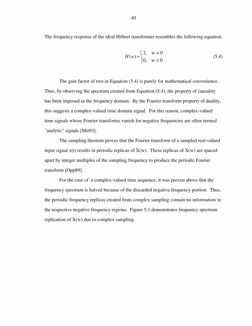
The frequency response of the ideal Hilbert transformer resembles the following equation.
0< w,0
0> w,2 )(
=wH (5.4)
The gain factor of two in Equation (5.4) is purely for mathematical convenience.
Thus, by observing the spectrum created from Equation (5.4), the property of causality
has been imposed in the frequency domain. By the Fourier transform property of duality,
this suggests a complex-valued time domain signal. For this reason, complex-valued
time signals whose Fourier transforms vanish for negative frequencies are often termed
"analytic" signals [Mit93].
The sampling theorem proves that the Fourier transform of a sampled real-valued
input signal x(t) results in periodic replicas of X(w). These replicas of X(w) are spaced
apart by integer multiples of the sampling frequency to produce the periodic Fourier
transform [Opp89].
For the case of a complex-valued time sequence, it was proven above that the
frequency spectrum is halved because of the discarded negative frequency portion. Thus,
the periodic frequency replicas created from complex sampling contain no information in
the respective negative frequency regions. Figure 5.1 demonstrates frequency spectrum
replication of X(w) due to complex sampling.

41
w
X(w)
w-wn n
X (w)s
w-w
= T
w
. . .
. . .
Nyquist
Nyquist
s
Figure 5.1 Spectrum of a Complex Signal Sampled at the Nyquist Rate
Figure 5.1 shows the frequency spectrum X(w) of a band-limited "analytic" signal
x(t). The second spectrum Xs(w) corresponds to the Fourier transform of the sampled
complex-valued time sequence, termed an "analytic" sequence.
The sampling theorem also states that the Nyquist sampling rate must be obeyed if
no aliasing occurs in the frequency domain. For real-valued signals, the Nyquist
frequency occurs at w = π/Ts. This corresponds to a Nyquist rate of fs = 2fmax.
However, for an "analytic" sequence it is readily apparent from Figure 5.1 that the
Nyquist rate can be reduced by a factor of two. This reduction stems from the fact that
the spectrum contains only positive frequency information. This "half-band" spectrum
allows the Nyquist frequency to be relaxed to a value of w = 2π/Ts. The corresponding
Nyquist sampling rate is reduced to fs = fmax without aliasing in the frequency domain.
Hence, the net effect of complex sampling a real-valued input signal results is an overall
relaxation of the Nyquist sampling rate by two.
42
Using the above arguments, the digital FM demodulator can use a sampling rate
equal to BFM /2 given in Equation (5.1). Aliasing will not occur if the FM signal is
complex sampled at a rate of BFM/2 samples/sec. Thus, the new FM bandwidth equation
becomes
BB
F BFMFM
complex 2 = = +
2( )∆ (5.5)
and the relaxed Nyquist sampling rate becomes
f B F Bs FMrelaxed complex 2(= = +∆ ) (5.6)
The reduction in the sampling rate due to complex sampling shown in Equation
(5.6) increases the FM signal bandwidth the demodulator can process while maintaining a
real-time processing window.
5.2 Computer Simulations of the FM Demodulator Algorithm
The digital FM demodulator was first tested using computer simulation. These
simulations provided a mapping from the algorithm theory into a working model. The
simulations also promoted a figure of merit for the FM demodulator algorithm.
Assuming no quantization error or finite math errors, the computer simulations provided
a sterile environment in order to classify the performance of the algorithm by itself.
Moreover, the final FM demodulator simulation acted as a template to translate the
demodulator model directly into DSP assembly code. Mathcad 4.0 was utilized to
simulate the demodulator algorithm. The simulations were first broken up into two
sessions: 1) The polar discriminator simulation and 2) The phase angle estimate

43
function simulation. Once these two simulations were verified to work as designed, they
were assembled as part of the final digital FM demodulator simulation. Each simulation
session can be found in the Appendix.
5.2.1 Polar Discriminator Simulation
The polar discriminator was simulated with a synthetic complex-valued input
signal. The input signal contained no modulation so the polar discriminator vectors had a
constant phase angle and could be correctly distinguished. A polar plot demonstrated that
the polar discriminator indeed operated properly and returned the correct phase difference
between two complex samples. The relevant graphs can be found in Appendix A.
However, as noted in Chapter 4, for a sinusoidal or nonlinear message m(t), the
polar discriminator does not return the exact phase derivative, but an approximation. The
differentiation error in the polar discriminator result is difficult to quantify, but will be
addressed in the testing phase of the demodulator since the message m(t) is generally a
sum of sinusoids or nonlinear function.
5.2.2 Phase Angle Estimate Simulation
The next simulation tested the phase angle estimate functions for all four
quadrants. A synthetic complex-valued signal was generated for 5000 phase angle points
spanning across quadrants I and II. The two interpolating phase angle estimate functions
were calculated for the angles native to their quadrant. The resulting phase angle
estimates were plotted against the true phase angles. The relative error accrued from the
phase angle estimates was treated as a random variable. Since the location of a given
phase angle is random in a modulated signal, the error of the estimated phase is also
random. In this case, the expected value of the relative error gives a measure of the
average error in an ensemble of complex data points. The average relative error for the

44
phase due to the phase estimator alone was shown to be 7.2%. This mean error figure is
relatively low and sufficiently accurate for the demodulator algorithm. During the
demodulator testing phase, this mean error figure can be expected to increase due to finite
word lengths, the sampling rate, and the statistics of the input signal. Recall that the
phase angle estimate functions have zero error only at the true phase angle points that
were used to construct the interpolating phase functions. If a high sampling rate or the
statistics of the input signal constrains the polar discriminator vectors to rotate within a
small area of a given quadrant, then the relative phase error can be large if the resulting
phase estimate is far away from the true data points used to create the interpolating phase
function. Moreover, the true phase angle points used in the construction of the
interpolating polynomials were equally distributed across their native quadrants. The data
points were distributed this way since the phase estimate function has to correctly classify
all phase angles as equally as possible. Because every phase angle is equally probable,
the interpolating function must account for an equally distributed error across each
quadrant. The equally distributed data points used in the Lagrange interpolation method
accounts for some minimization of this error. The polar plot in Figure 5.2 is a replica of
the phase error plot in Appendix B. Figure 5.2 accentuates the areas in each quadrant
where the phase estimate error is large.
The probability of consecutive vectors residing in a large error region of the phase
estimate function unilaterally depends on the statistics of the FM input signal and is
therefore analytically unsolvable. However, as long as the Nyquist rate is maintained, the
relative phase error will be approximately 7.2% on average. Also, sampling the input
signal greater than the Nyquist rate increases the probability that a given vector will lie in
a large error region of the phase estimate function. This is an artifact of the Lagrange
polynomial construction. If the sampling rate constrains the vectors to migrate about an
area that induces a large error in the phase estimate, the overall phase estimate error will
increase.

45
0
22.5
45
67.5
90
112.5
135
157.5
180
202.5
225
247.5
270
292.5
315
337.5
0.785
1.57
2.356
3.141
phasen
arg sign
phasen
arg sign
,,,.n
Nπ .n
Nπ .n
Nπ .n
Nπ
Figure 5.2 Polar Plot of the Phase Angle Estimates Versus True Phase Angles
5.2.3 FM Demodulator Algorithm Simulation
The FM demodulator algorithm simulation was analyzed at the Nyquist sampling
rate -- the maximum sampling rate for which the demodulator can operate. The
modulated input message m(t) injected into the FM demodulator was chosen as a 1 kHz
sinusoid. The sinusoidal message permits an easy first-order analysis of the demodulator
performance. The complex mixing operation and complex sampling operation was
simulated by creating a complex baseband FM signal through the use of Equation (2.21).
The P(t) signal was generated in the simulation for simplicity. Also, an oscillatory AM
noise signal was generated and added to the baseband FM signal to demonstrate the

46
function of the digital limiter. Upon demodulation, the message m(t) appeared as the
derivative of P(t), as given by Equation (2.4). The resulting amplitude of the message
m(t) was calculated and verified in the simulation.
Polar discriminator and digital limiter
The FM demodulator simulation established that the polar discriminator
calculated the phase difference between successive complex FM samples. These phase
vectors deviate up to 180°, verifying the Nyquist sampling rate. Also, the digital limiter
effectively eliminated the AM noise present in the phase vectors and passed the results to
the phase estimate functions. The relevant graphs are shown in Appendix C.
Phase estimate errors
The resulting mean phase estimate error was approximately 4%. This error
figure is lower than the calculated phase error shown in the phase angle estimate
simulation. However, the statistics of the input FM signal can cause the phase vectors to
reside around a low error region in the interpolating phase polynomial, thus explaining
the low phase error.
Spectral analysis
Discrete phase errors are difficult to measure while the FM demodulator is being
tested. Hence, a spectral purity test was simulated to measure a theoretical versus
practical signal-to-noise ratio (SNR) for the demodulated message. The spectral
simulation demonstrated that at the Nyquist rate, the algorithm suffered a minimum 5 dB

47
loss in the SNR ratio due to the demodulator algorithm. Figure 5.3 is a replica of the
spectral simulation plot found in Appendix C. From Figure 5.3, it is evident that
harmonics of the message frequency were responsible for the SNR loss. In fact, only the
odd harmonics were accountable for the noise. These corrupting harmonics give the FM
demodulator algorithm a minimum SNR error expected after implementation. The
harmonic distortion due to the demodulator algorithm can be attributed to the
differentiation error from the polar discriminator and the phase estimate error. Because
of the complexity of analyzing the system error, the simulation is unable to delineate
which error contributes the most to the harmonic distortion.
0 1000 2000 3000 4000 5000 6000 7000 8000 90001 104120
109.704
99.409
89.113
78.817
68.522
58.226
log Zk
k
.N_pad T
Figure 5.3 Spectral Analysis Plot of the Demodulated Message
The final FM simulation gave sufficient results and demonstrated that the
mathematical model of the FM demodulator worked as designed. The system error in the
demodulated message demonstrates the classic tradeoff of algorithm speed versus
accuracy. Since this FM demodulator algorithm was geared for speed, some error must

48
be tolerated. The next step was to translate the final FM demodulator simulation into
DSP assembly code in order to run on the digital radio board.
5.3 Realization of the FM Demodulator into DSP Code
From the FM demodulator block diagram in Figure 4.5, the number of necessary
mathematical operations to process one complex FM sample can be readily determined.
The polar discriminator block requires one complex multiply, which translates to four
real multiplies and two additions. Likewise, the digital limiter needs two additions and
one division. Finally, the phase estimator block requires one real multiply and one
addition. So, demodulating a complex-sampled FM signal requires the following
operations per sample: Five real multiplies, five real additions, and one division.
5.3.1 DSP Computational Overhead
The FM demodulator was directly implemented into ADSP-2101 assembly code
using the final Mathcad simulation as a template. The software listing is included in the
Appendix. The polar discriminator was implemented in 19 DSP assembly instructions
(62.5 ns per instruction cycle). The digital limiter was implemented in 25 DSP
instructions. The phase angle estimator was implemented with 10 instructions for the
quadrant I estimate and 14 instructions for the quadrant II estimate. Thus, the
computational overhead was approximately 54-58 DSP instructions per complex sample
for the FM demodulator. This overhead does not include the time to fetch a new complex
sample from the GC1011. Chapter 3 stated that the GC1011 chip was "polled" for new
samples. The GC1011 software overhead is about 30 DSP instructions, which
corresponds to (30)*62.5 ns = 1.875 µs of extra overhead for processing each sample.
Also, the DAC interrupt service routine requires 10 DSP instructions, or 625 ns. Hence,

49
the worst-case time it takes the DSP to process one complex sample is (58)*62.5 ns +
625 ns + 1.875 µs = 6.125 µs. This calculated time defines the maximum sampling rate
for the demodulator and also the real-time operating window. The demodulator will fall
out of real-time operation if the incoming samples arrive faster than f = 1 / 6.125 µs =
163.3 kHz. Moreover, from Equation (5.6) this sampling rate also defines the total FM
signal bandwidth able to be processed by the digital FM demodulator.
5.3.2 Quantization Errors and Best-Case SNR
As mentioned in Chapter 3, the front-end A/D converter has a resolution of 8 bits.
This corresponds to a theoretical 8(6 dB) = 48 dB of SNR using the 6-dB rule. Moreover,
the GC1011 rounds the complex samples sent to the DSP to 16 bits, and the back-end
DAC has a resolution of 12 bits. Therefore, quantization error, finite-word lengths, and
rounding have an effect on the algorithm system error.
The phase estimate function coefficients were realized with 12-bit precision. This
precision was chosen because it prevented overflow and the need for saturation
arithmetic. Hence, there is an inherent error by quantizing the phase function coefficients
to 12 bits. However, it was calculated that the relative error in the coefficients was at
most 0.03%, which can be neglected as a source of significant error.
Equation (2.21) shows that after the mixing operation, a baseband FM signal has
half of its original amplitude. Unfortunately, the GC1011 does not account for this "half-
power" loss. Because of this fact, the GC1011 is responsible for an additional 6 dB of
SNR loss before the DSP processes the data.1 Therefore, the GC1011 effectively drops
one bit of available SNR resolution, resulting in 7 bits of actual SNR resolution.
Therefore, due to finite-word lengths, the best-case theoretical SNR the digital radio
board can offer is 7(6 dB) = 42 dB.
1Excerpt from a conversation with Joe Gray of Graychip, Inc.
50
5.4 Testing the FM Demodulator
The developed DSP code was compiled and downloaded into a boot EPROM. On
system powerup, the DSP on the digital radio board uploads the boot EPROM contents,
initializes the hardware, and begins execution of the demodulator software.
5.4.1 Digital Radio Software and Testing Setup
The DSP initialized the GC1011 digital receiver chip to decimate the incoming
RF digital data to 50 Ksamples/sec., which corresponds to a sampling rate of 50 kHz for
the DSP. This sampling rate is well within the real-time computational window of the
demodulator code. The DSP also set the GC1011 tune frequency to a carrier frequency of
21.4 MHz -- a common IF output of an analog receiver. An RF signal generator was used
to create a 1 kHz sine wave message signal m(t). This message mocks the synthetic
signal used in the demodulator simulation. The resulting FM signal from the signal
generator had a carrier frequency of 21.4 MHz, and it was used as the input to the digital
radio board. The optimal amplitude for the FM input signal was determined to be -1.0
dBm through heuristic methods. By Equation (5.7), the 1 kHz sine wave message and the
50 kHz sampling rate indicates a maximum FM frequency deviation of ∆F = 24 kHz.
Thus, surpassing a frequency deviation of ∆F = 24 kHz while testing will result in
aliasing. The AM noise was unable to be fabricated in the laboratory, but the simulation
proved that the algorithm works correctly with or without the presence of AM noise.
5.4.2 SNR Measurements
As discussed in the spectral analysis simulation section, a spectrum analyzer was
used to measure the SNR due to harmonic distortion for the digital FM demodulator. The
frequency deviation of the FM signal was stepped from ∆F = 1 kHz to ∆F = 24 kHz in 1
kHz increments via the RF generator.

51
The original 1 kHz message signal was successfully demodulated by the digital
radio, and the digital FM demodulator output from the onboard DAC was observed on the
spectrum analyzer for purity. Depending on the frequency deviation, the worst-case SNR
due to harmonic distortion was 24 dB. The best-case SNR was observed to be 36 dB.
Since the spectrum analyzer output had no printing capability, the uncertainty in the SNR
measurements were ±1 dB. Table 5.1 shows the SNR figures for each increment of the
frequency deviation. The table also lists the message signal strength and the largest
corrupting harmonic for each SNR measurement taken.
Table 5.1 Frequency Deviations and FM Demodulator SNR Measurements
Frequency
deviation ∆F (kHz)
1 kHz message
amplitude (dB)
SNR (dB) Largest corrupting
harmonic
1 -8 32 3rd
2 -2 29 3rd
3 0 26 3rd
4 2 24 3rd
5 4 24 3rd
6 6 24 3rd
7 7 26 3rd
8 8 26 3rd
9 9 27 3rd
10 10 29 3rd
11 10 30 3rd
12 11 31 5th
13 12 30 5th
14 12 30 5th
15 14 34 3rd, 5th, 7th
16 15 33 7th
17 16 34 7th
18 17 36 7th
19 17 34 7th
20 17 33 5th
21 17 32 5th
22 17 31 3rd
23 17 30 3rd
24 17 aliased aliased

52
The test data in Table 5.1 agrees with the findings in the computer simulations.
Specifically, the following observations directly correlates the test data to the simulation
results.
• The major corrupting harmonics in the demodulated message were the odd
harmonics.
• The range of SNR numbers in Table 5.1 is 24 dB to 36 dB. Recall, the
frequency deviation of the FM signal directly effects the SNR of the
demodulated message. It was shown before that the best-case SNR for the
digital radio was 42 dB. Moreover, the demodulator simulation verified that
there is at least a 5 dB SNR loss due to the algorithm itself. Consequently,
this imposes a best-case theoretical SNR for the FM demodulator of 37 dB.
The test data verifies that the demodulator never reaches the 37 dB theoretical
SNR figure but comes close. The small difference from the theoretical SNR
to the measured SNR can be attributed to losses inherent to the digital radio
board, such as finite arithmetic and rounding errors.
• The test data also justifies the fact that the system error increases (i.e., the
SNR figures decrease) by varying the FM frequency deviation. It was
revealed previously that decreasing the frequency deviation below the Nyquist
rate causes the statistics of the FM signal to change and thus allowing the
phase vectors to reside in a high error region of the phase estimate functions.
• With a 50 kHz sampling rate, the demodulator experienced aliasing at ∆F = 24
kHz. This value is consistent with the expected Nyquist rate.
The demodulator produced satisfying results using the first-order phase estimate
functions. The test data concurs with the initial findings in the computer simulations.
Specifically, the error in the demodulated message fluctuated significantly in some cases,
but the demodulator algorithm knowingly traded accuracy for speed.
Therefore, the realization of the digital FM demodulator proved successful, and
the corresponding test results demonstrated that the algorithm theory was correctly
implemented and the demodulator operated up to the design expectations.
53
CHAPTER 6
CONCLUSION AND FUTURE DEVELOPMENT
This thesis presented the design of a digital FM demodulator as implemented on a
digital radio. The concepts of digital signal processing allowed a common analog FM
demodulator to be mathematically modeled and transformed into an equivalent digital
version. The algorithm was first prototyped using computer simulations. These
simulations verified that the algorithm integrity was preserved from theory to realization.
The digital FM demodulator was then implemented with DSP software and executed in
real time on the digital radio board. The FM demodulator was able to effectively
demodulate narrowband FM signals. Wideband FM signals were not targeted due to the
speed limitations of the digital radio board. However, the digital FM demodulator proved
to be a stepping stone to other common narrowband demodulator schemes implementable
on the digital radio.
Examples of several "next-step" demodulators that can be readily implemented
using the digital radio and DSP techniques are listed below.
• An AM demodulator can be realized on the digital radio by simply passing the
incoming complex baseband samples through a function that estimates
Equation (4.2).
• A frequency-shift keying (FSK) algorithm consists of the functional blocks in
Figure 4.6 without the phase angle estimate block. Since FSK only uses two
modulating frequencies, the true phase angle is unnecessary.
• Multilevel signaling techniques, like quadrature-amplitude modulation (QAM)
can be realized by adding the AM demodulator listed above to the block
diagram shown in Figure 4.6.
54
The FM demodulator designed in this paper can be modified to improve its
overall performance. Development of a more accurate phase angle estimator is the
obvious solution for improving the algorithm performance. Methods such as a Taylor
series expansion for the arctangent function in Equation (4.3) or a look-up table will
improve the accuracy of the phase angle estimator. However, such modifications will
trade program execution speed for the improved accuracy. Consequently, this loss in
speed implies a reduction in the FM signal bandwidth the digital radio can process.
The maturation of the digital radio hardware also plays a role in the software
development. A faster DSP and a faster data transfer rate between the digital receiver
chip and the DSP will allow a larger RF bandwidth to be processed. Hence, wideband
FM modulation and other high-bandwidth communications can be targeted with a higher
speed digital radio board. The digital radio will replace the conventional analog receiver
when the evolution of the digital radio reaches a point where high bandwidth, multiple-
channel communication schemes can be targeted and demodulated through the use of
DSP code.
55
APPENDIX A
SIMULATION OF THE POLAR DISCRIMINATOR
The following is the Mathcad 4.0 simulation session for the polar discriminator
utilized in the digital FM demodulator. The session was executed on a PC Windows-
based software platform.

56
57
APPENDIX B
SIMULATION OF THE PHASE ANGLE ESTIMATE FUNCTIONS
The following is the Mathcad 4.0 simulation session for the phase angle estimate
functions utilized in the digital FM demodulator. The session was executed on a PC
Windows-based software platform.

58
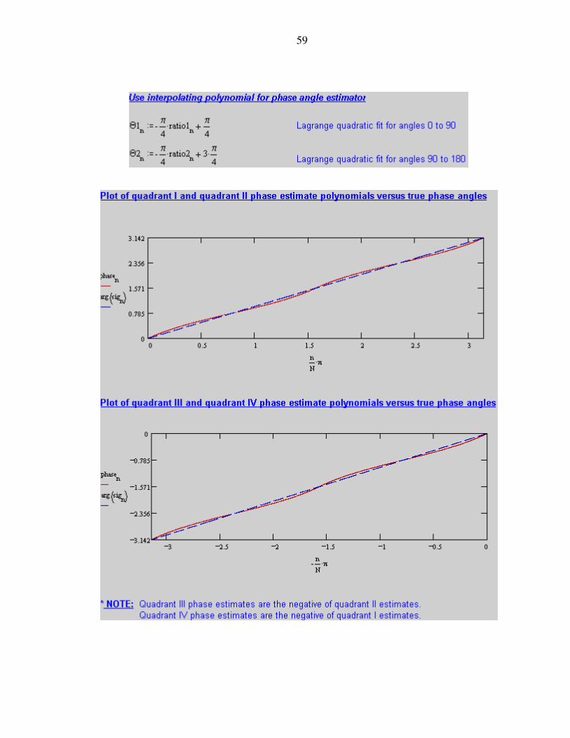
59

60

61

62
APPENDIX C
SIMULATION OF THE DIGITAL FM DEMODULATOR
The following is the Mathcad 4.0 simulation session for the final design of the
digital FM demodulator. All previous Mathcad simulations were assembled to create the
framework for this final simulation environment. The session was executed on a PC
Windows-based software platform.

63

64

65

66
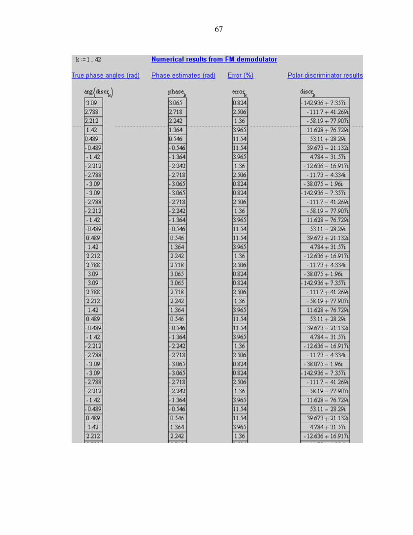
67

68

69
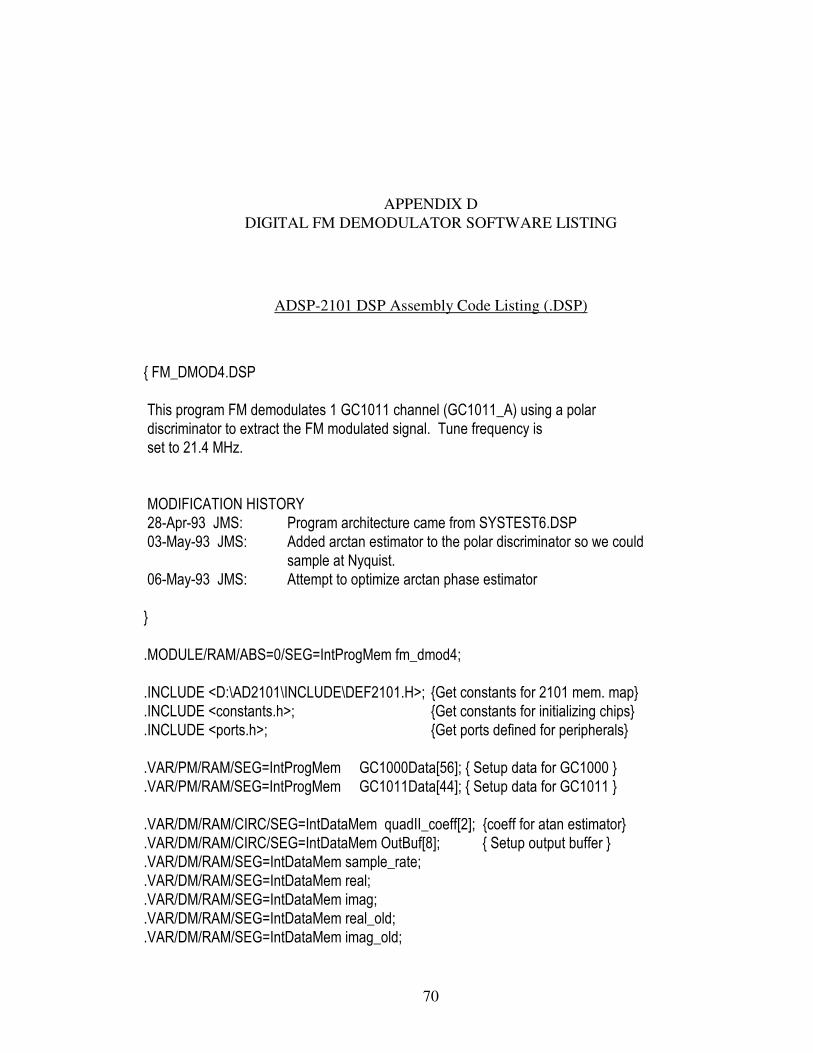
70
APPENDIX D
DIGITAL FM DEMODULATOR SOFTWARE LISTING
ADSP-2101 DSP Assembly Code Listing (.DSP)
{ FM_DMOD4.DSP
This program FM demodulates 1 GC1011 channel (GC1011_A) using a polar
discriminator to extract the FM modulated signal. Tune frequency is
set to 21.4 MHz.
MODIFICATION HISTORY
28-Apr-93 JMS: Program architecture came from SYSTEST6.DSP
03-May-93 JMS: Added arctan estimator to the polar discriminator so we could
sample at Nyquist.
06-May-93 JMS: Attempt to optimize arctan phase estimator
}
.MODULE/RAM/ABS=0/SEG=IntProgMem fm_dmod4;
.INCLUDE <D:\AD2101\INCLUDE\DEF2101.H>; {Get constants for 2101 mem. map}
.INCLUDE <constants.h>; {Get constants for initializing chips}
.INCLUDE <ports.h>; {Get ports defined for peripherals}
.VAR/PM/RAM/SEG=IntProgMem GC1000Data[56]; { Setup data for GC1000 }
.VAR/PM/RAM/SEG=IntProgMem GC1011Data[44]; { Setup data for GC1011 }
.VAR/DM/RAM/CIRC/SEG=IntDataMem quadII_coeff[2]; {coeff for atan estimator}
.VAR/DM/RAM/CIRC/SEG=IntDataMem OutBuf[8]; { Setup output buffer }
.VAR/DM/RAM/SEG=IntDataMem sample_rate;
.VAR/DM/RAM/SEG=IntDataMem real;
.VAR/DM/RAM/SEG=IntDataMem imag;
.VAR/DM/RAM/SEG=IntDataMem real_old;
.VAR/DM/RAM/SEG=IntDataMem imag_old;

71
.VAR/DM/RAM/SEG=IntDataMem quadI_coeff;
.INIT GC1000Data: <GC1000_A.dat>; { Init. PM w/GC1000 setup }
.INIT GC1011Data: <GC1011FM.dat>; { Init. PM w/GC1011 setup }
{ .INIT quadII_coeff: H#0324, H#096C; }
{* interrupt jump vector table *}
JUMP MAIN; nop; nop; nop; { reset interupt }
JUMP OUTDATA; nop; nop; nop; { interrupt for DACs }
RTI; nop; nop; nop; { SPORT0 transmit interupt }
RTI; nop; nop; nop; { SPORT0 receive interupt }
RTI; nop; nop; nop; { IRQ1 interupt }
RTI; nop; nop; nop; { IRQ0 interupt }
RTI; nop; nop; nop; { timer interupt }
{* Executable code: *}
MAIN: AX0=0; { initialize DM variables }
DM(real)=AX0;
DM(imag)=AX0;
DM(real_old)=AX0;
DM(imag_old)=AX0;
AX0=H#0C90; { quadI coeff = 0.785 / 8 coeff to }
DM(quadI_coeff)=AX0; { prevent overflow }
{* NOTE: quadII coeffs are 1st scaled < 1 and then / 8 to prevent overflow *}
I0=^quadII_coeff;
M0=1;
L0=%quadII_coeff;
AX0=H#0324; { 3.13 format for numbers > 1 }
DM(I0,M0)=AX0;
AX0=H#096C;
DM(I0,M0)=AX0;
AX0=0x00F9; { set for 50kHz output rate to DAC }
DM(sample_rate)=AX0; { for initial FM bandwidth }
AX0=0x001F; { Setup the system control register }
DM(Sys_Ctrl_Reg)=AX0; { SPORT's disabled, Boot page=0 }
AX0=0x35FF; { Setup the wait states for DM space }
DM(Dm_Wait_Reg)=AX0; { DWAIT3=2,DWAIT4=3, all others 7 }
MSTAT = 0; { setup FRACTIONAL results for MAC}

72
IFC = B#000000111111; {Clear out any interupts, }
ICNTL = B#00111; { setup IRQ2,IRQ1,IRQ0 as edge trig }
IMASK=0; { disable all irqs}
L0 = 0; { Set all the circular buffer }
L1 = 0; { registers to be linear }
L2 = 0; { addressing }
L3 = 0;
L4 = 0;
L5 = 0;
L6 = 0;
L7 = 0;
{* Setup the GC1000 chip. Transfer data from program memory to the chip. *}
M0=1; { Setup I0 to step one by one }
I0=GC1000; { beginning at GC1000's Base Addr.}
L4=0;
M4=1; { Setup I4 to step one by one }
I4=^GC1000Data; { through PM GC1000 Setup data }
CNTR=%GC1000Data; { Transfer all data in PM }
DO SETUP1 UNTIL CE;
AX0=PM(I4,M4); { Grab value from PM and }
SETUP1: DM(I0,M0)=AX0; { move it to DM }
{* Setup the GC1011's to their default values. See the GC1011.DAT file for
the default setup information. *}
I0=GC1011A; { Get base addr. of GC1011-A }
I4=^GC1011Data; { Get base addr. of GC1011 setup data }
CNTR=11; { Transfer the 11 bytes of setup }
DO SETUP2 UNTIL CE;
AX0=PM(I4,M4); { data from PM (AX0 temp. holds it) }
SETUP2: DM(I0,M0)=AX0; { to GC1011 }
I0=GC1011B; { Get base addr. of GC1011-B }
CNTR=11; { Transfer the 11 bytes of setup }
DO SETUP3 UNTIL CE;
AX0=PM(I4,M4); { data from PM (AX0 temp. holds it) }
SETUP3: DM(I0,M0)=AX0; { to GC1011 }
I0=GC1011C; { Get base addr. of GC1011-C }
CNTR=11; { Transfer the 11 bytes of setup }
DO SETUP4 UNTIL CE;
AX0=PM(I4,M4); { data from PM (AX0 temp. holds it) }

73
SETUP4: DM(I0,M0)=AX0; { to GC1011 }
I0=GC1011D; { Get base addr. of GC1011-D }
CNTR=11; { Transfer the 11 bytes of setup }
DO SETUP5 UNTIL CE;
AX0=PM(I4,M4); { data from PM (AX0 temp. holds it) }
SETUP5: DM(I0,M0)=AX0; { to GC1011 }
{* setup the programmable counter to the output clock frequency rate }
DM(Count_Xtrset)=AX0; { Set XTR line on 74F525 to stop }
DM(Count_rst)=AX0; { clocking the counter then reset it }
AX0=DM(sample_rate); { Get the DAC's clocking frequency }
DM(Counter)=AX0; { and send it to the 74F525 }
DM(Count_Xtrclr)=AX0; { Re-enable clocking by clearing XTR }
M4 = 1; { Address generator I4 will be the }
I4 = ^OutBuf; { GC1011 input side of the circular }
L4 = %OutBuf; { output buffer }
I5 = ^OutBuf; { I5 will be DAC output side of the }
L5 = %OutBuf; { buffer. }
M5 = 1;
M1 = -1; { M1 will decr. address values }
I1 = GC1011A + QOutput1; { Get addr. of MSB of Q output data. }
L1=0;
I7 = ^quadII_coeff; { pointers for poly coeffs}
M7 = 1;
L7 = %quadII_coeff;
{* Loop to poll the GC1011s *}
{* Recall: IRQ2 = interrupt for DACs *}
IMASK=B#100000; { turn on IRQ2 }
TEST: AY0=1; { bit 0 mask }
AX0 = DM(OutstatA); { Get status of GC1011's output reg }
AR = AX0 AND AY0; { If data is ready then lets get it }
IF NE JUMP TEST; { keep waiting }
CALL GETDATA; { Go get two data words from GC1011 }
CALL POLAR_DISCR; { demodulate FM signal }
JUMP TEST;
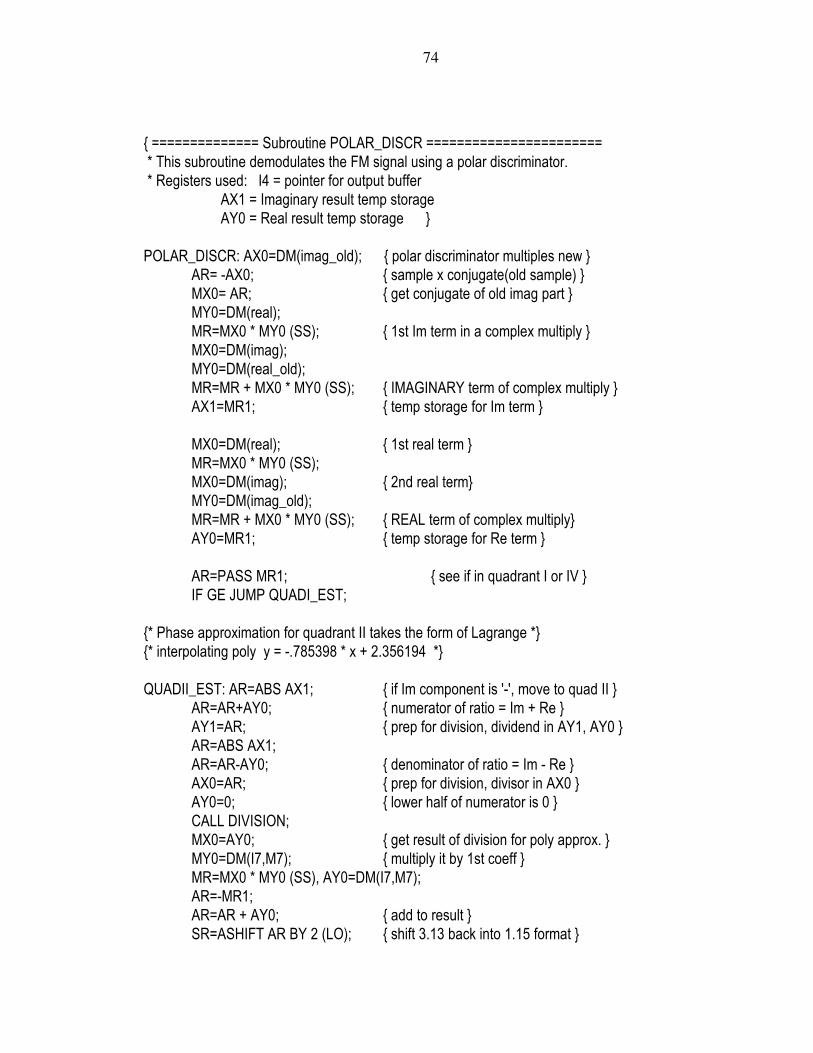
74
{ ============== Subroutine POLAR_DISCR =======================
* This subroutine demodulates the FM signal using a polar discriminator.
* Registers used: I4 = pointer for output buffer
AX1 = Imaginary result temp storage
AY0 = Real result temp storage }
POLAR_DISCR: AX0=DM(imag_old); { polar discriminator multiples new }
AR= -AX0; { sample x conjugate(old sample) }
MX0= AR; { get conjugate of old imag part }
MY0=DM(real);
MR=MX0 * MY0 (SS); { 1st Im term in a complex multiply }
MX0=DM(imag);
MY0=DM(real_old);
MR=MR + MX0 * MY0 (SS); { IMAGINARY term of complex multiply }
AX1=MR1; { temp storage for Im term }
MX0=DM(real); { 1st real term }
MR=MX0 * MY0 (SS);
MX0=DM(imag); { 2nd real term}
MY0=DM(imag_old);
MR=MR + MX0 * MY0 (SS); { REAL term of complex multiply}
AY0=MR1; { temp storage for Re term }
AR=PASS MR1; { see if in quadrant I or IV }
IF GE JUMP QUADI_EST;
{* Phase approximation for quadrant II takes the form of Lagrange *}
{* interpolating poly y = -.785398 * x + 2.356194 *}
QUADII_EST: AR=ABS AX1; { if Im component is '-', move to quad II }
AR=AR+AY0; { numerator of ratio = Im + Re }
AY1=AR; { prep for division, dividend in AY1, AY0 }
AR=ABS AX1;
AR=AR-AY0; { denominator of ratio = Im - Re }
AX0=AR; { prep for division, divisor in AX0 }
AY0=0; { lower half of numerator is 0 }
CALL DIVISION;
MX0=AY0; { get result of division for poly approx. }
MY0=DM(I7,M7); { multiply it by 1st coeff }
MR=MX0 * MY0 (SS), AY0=DM(I7,M7);
AR=-MR1;
AR=AR + AY0; { add to result }
SR=ASHIFT AR BY 2 (LO); { shift 3.13 back into 1.15 format }

75
AR=SR0;
AF=PASS AX1; { check Im result to see if quad II or III }
IF LT AR=-SR0; { if Im is in quad 3, negate phase answer }
JUMP PHASE_EST;
{* Phase approximation for quadrant I takes the form of Lagrange *}
{* interpolating poly y = -0.785398 * x + 0.785398 *}
QUADI_EST: AF=ABS AX1; { if Im part is '-', put in quad I }
AR=MR1-AF; { numerator for ratio = Re - Im }
AY1=AR; { prep for division, dividend in AY1 }
AX0=AY0; { move Re component }
AR=AX0+AF; { denominator is Re + Im }
AX0=AR; { divisor is in AX0 }
AY0=0;
CALL DIVISION;
MX0=AY0;
MY0=DM(quadI_coeff);
MR=MX0 * MY0 (SS), AY0=MY0;
AR=-MR1;
AR=AR + AY0; { add to result }
AF=PASS AX1; { check Im result to see if quad I or IV }
IF LT AR=-AR; { if in quad 4, negate phase answer }
PHASE_EST: SR=ASHIFT AR BY 1 (LO); { add max gain to prevent DAC overflow }
DM(I4,M4)=SR0; { store phase result to out buffer}
{* Store current sample as old sample for next discriminator calculation }
AX0=DM(real); { get current real part }
DM(real_old)=AX0;
AX0=DM(imag); { get current imaginary part }
DM(imag_old)=AX0;
RTS;
{=====================================================}
DIVISION: DIVS AY1,AX0;
DIVQ AX0; DIVQ AX0; DIVQ AX0; DIVQ AX0; DIVQ AX0; DIVQ AX0;
DIVQ AX0; DIVQ AX0; DIVQ AX0; DIVQ AX0; DIVQ AX0; DIVQ AX0;
DIVQ AX0; DIVQ AX0; DIVQ AX0;
RTS;

76
{ =============== Subroutine GetData ======================
* This subroutine will read the imaginary and real data value from the
* GC1011. The routine reads the MSB of the Q-value, shifts it and then
* concatenates the LSB. The same thing is done with the real value.
* the results are stored using address in I4.
* Registers Used.....
I1 = Address where MSB Q value for the GC1011 is
M1 = -1, so address is decremented to get Q and I values from GC1011
I4 = Address where results are stored.
M4 = Increment I4's address by one.
AX0, AX1, AY0, AF, AR, SR are used in computation. }
GETDATA: SI = DM(I1,M1); { Get the MSByte from GC1011 and }
SR = LSHIFT SI BY 8 (LO); { move this to MSB of 16 bit value }
AX0 = DM(I1,M1); { Get the LSByte and clear the MSByte }
AY0 = 0x00FF; { Value to zero out MSB's }
AF = AX0 AND AY0; { to zero. Append this to GC1011's }
AR = SR0 OR AF; { MSByte to form 16 bit word }
AX1 = AR; { Temp. store Q results in AX1 }
SI = DM(I1,M1); { Get the MSByte from GC1011 and }
SR = LSHIFT SI BY 8 (LO); { move this to MSB of 16 bit value }
AX0 = DM(I1,M1); { Get the LSByte and clear the MSByte }
AF = AX0 AND AY0; { to zero. Append this to GC1011's }
AR = SR0 OR AF; { MSByte to form 16 bit word }
DM(real) = AR; { Store real value first (I reg.) }
DM(imag) = AX1; { Store imaginary (Q reg.) }
I1 = GC1011A + QOutput1; { Reset addr. of GC1011's Q output. }
AY0 = 1; { Reset the value of AY0 }
AX0 = DM(OutstatA); { Get GC1011's status and }
AR = AX0 OR AY0; { set the data ready bit. }
DM(OutstatA) = AR; { Send this back to the GC1011 }
RTS; { and go back to work }

77
{ =========== OutData interrupt service routine ========================
* This service routine will take a data value from a buffer and output it to
* DAC1.
* Registers Used.....
I5 = Address where results are stored.
M5 = Increment I5's address by one.
SI = Temporary holding register. }
OUTDATA: ENA SEC_REG; { enable secondary registers to}
{ preserve registers before IRQ}
SI = DM(I5,M5); { Get value to send to DAC }
SR = LSHIFT SI BY -4 (LO); { Convert 16 bit value to 12 bit }
AY1 = H#0800; { Convert this 2's complement word }
AR = SR0 XOR AY1; { to offset binary for DAC }
DM(DAC_1) = AR;
DIS SEC_REG;
RTI;
.ENDMOD; { Complete the module }

78
ADSP-2101 System Builder File (.SYS)
.SYSTEM fm_dmod4;
.ADSP2101;
.MMAP0;
.SEG/PM/RAM/ABS=0x0000/CODE/DATA IntProgMem[2048];
.SEG/PM/RAM/ABS=0x0800/CODE/DATA ExtProgMem[14336];
.SEG/DM/RAM/ABS=0x0000 ExtDataMem[12288];
.SEG/DM/RAM/ABS=0x03800 IntDataMem[1024];
.SEG/ROM/BOOT=0 boot_mem[2048];
{* ports for the memory-mapped peripherals in the DM map *}
.PORT/DM/ABS=0x03280 Counter;
.PORT/DM/ABS=0x03300 DAC_1;
.PORT/DM/ABS=0x03301 DAC_2;
.PORT/DM/ABS=0x03380 DAC_3;
.PORT/DM/ABS=0x03381 DAC_4;
{ specific ports for the DUART }
.PORT/DM/ABS=0x03400 Mode_regA;
.PORT/DM/ABS=0x03401 Status_clk_regA;
.PORT/DM/ABS=0x03402 ISR_Cmd_regA;
.PORT/DM/ABS=0x03403 Data_regA;
.PORT/DM/ABS=0x03404 IPCR_ACR_reg;
.PORT/DM/ABS=0x03405 ISR2_IMR_reg;
.PORT/DM/ABS=0x03408 Mode_regB;
.PORT/DM/ABS=0x03409 Status_clk_regB;
.PORT/DM/ABS=0x0340A Cmd_regB;
.PORT/DM/ABS=0x0340B Data_regB;
.PORT/DM/ABS=0x0340C IVR_reg;
.PORT/DM/ABS=0x0340D In_OPCR_reg;
.PORT/DM/ABS=0x0340E Go_cnt_set_out;
.PORT/DM/ABS=0x0340F Stop_cnt_clr_out;
79
{ specific ports for the 4 GC1011 receiver chips }
{GC1011A chip}
.PORT/DM/ABS=0x0308F Qout1A;
.PORT/DM/ABS=0x0308E Qout0A;
.PORT/DM/ABS=0x0308D Iout1A;
.PORT/DM/ABS=0x0308C Iout0A;
.PORT/DM/ABS=0x0308A OutstatA;
{GC1011B chip}
.PORT/DM/ABS=0x0310F Qout1B;
.PORT/DM/ABS=0x0310E Qout0B;
.PORT/DM/ABS=0x0310D Iout1B;
.PORT/DM/ABS=0x0310C Iout0B;
.PORT/DM/ABS=0x0310A OutstatB;
{GC1011C chip}
.PORT/DM/ABS=0x0318F Qout1C;
.PORT/DM/ABS=0x0318E Qout0C;
.PORT/DM/ABS=0x0318D Iout1C;
.PORT/DM/ABS=0x0318C Iout0C;
.PORT/DM/ABS=0x0318A OutstatC;
{GC1011D chip }
.PORT/DM/ABS=0x0320F Qout1D;
.PORT/DM/ABS=0x0320E Qout0D;
.PORT/DM/ABS=0x0320D Iout1D;
.PORT/DM/ABS=0x0320C Iout0D;
.PORT/DM/ABS=0x0320A OutstatD;
{ ports to control the counter }
.PORT/DM/ABS=0x03289 Count_rst;
.PORT/DM/ABS=0x03291 Count_Xtrset;
.PORT/DM/ABS=0x03299 Count_Xtrclr;
.ENDSYS;

80
REFERENCES
[Ana90] Analog Devices, ADSP-2101 User's Manual, 1st Edition. Analog
Devices, Norwood, MA, February 1990.
[Cou90] Couch, Leon W. Digital and Analog Communication Systems, 3rd
Edition. Macmillan Publishing Company, New York, 1990.
[Gra91] Graychip, GC1011 Digital Receiver Chip Data Sheet. Graychip, Inc., Palo
Alto, CA, May 1991.
[Hag88] Hager, William W. Applied Numerical Linear Algebra. Prentice Hall,
Englewood Cliffs, NJ, 1988.
[Mit93] Mitra, Sanjit, & Kaiser, James. Handbook for Digital Signal Processing.
John Wiley & Sons, New York, 1993.
[Opp89] Oppenheim, Alan, & Schafer, Ronald. Discrete-Time Signal Processing.
Prentice Hall, Englewood Cliffs, NJ, 1989.
[Str88] Strum, Robert, & Kirk, Donald. Discrete Systems and Digital Signal
Processing. Addison-Wesley Publishing Company, Reading, MA, 1988.

81
BIOGRAPHICAL SKETCH
The author was born in Cleveland, Ohio, on February 4, 1969. He received his
Bachelor of Science in Electrical Engineering degree in December of 1992 from the
University of Florida. He returned to the University of Florida in August of 1993 to
pursue a master's degree in electrical engineering. He is scheduled to receive a Master of
Science degree in May of 1995.
Throughout his undergraduate and graduate career, the author completed five
cooperative education tours with the Central Intelligence Agency in Langley, Virginia,
where he was exposed to digital communications and DSP applications. During his
graduate program, he also worked as a graduate teaching assistant for the Digital Design
Lab.
He will be pursuing a career in DSP applied research in the private or government
sector following graduation.

I certify that I have read this study and that in my opinion it conforms to
acceptable standards of scholarly presentation and is fully adequate, in scope and quality,
as a thesis for the degree of Master of Science.
________________________________
Scott L. Miller, Chairman
Associate Professor of Electrical
Engineering
I certify that I have read this study and that in my opinion it conforms to
acceptable standards of scholarly presentation and is fully adequate, in scope and quality,
as a thesis for the degree of Master of Science.
________________________________
Jose C. Principe, Co-chairman
Professor of Electrical Engineering
I certify that I have read this study and that in my opinion it conforms to
acceptable standards of scholarly presentation and is fully adequate, in scope and quality,
as a thesis for the degree of Master of Science.
________________________________
Michel A. Lynch
Lecturer of Electrical Engineering
This thesis was submitted to the Graduate Faculty of the College of Engineering
and to the Graduate School and was accepted as partial fulfillment of the requirements for
the degree of Master of Science.
May 1995 ________________________________
Winfred M. Phillips
Dean, College of Engineering
________________________________
Dean, Graduate School