chapter 5 digital bandpass modulation and demodulation ...silage/chapter5ms.pdf · ee4512 analog...
TRANSCRIPT

EE4512 Analog and Digital Communications Chapter 5
Chapter 5Chapter 5
Digital Bandpass ModulationDigital Bandpass Modulationand Demodulationand DemodulationTechniquesTechniques

EE4512 Analog and Digital Communications Chapter 5
Chapter 5Chapter 5
Digital Bandpass ModulationDigital Bandpass Modulationand Demodulationand DemodulationTechniquesTechniques•• Binary Amplitude Shift KeyingBinary Amplitude Shift Keying
•• Pages 212Pages 212--219219
EE4512 Analog and Digital Communications Chapter 5
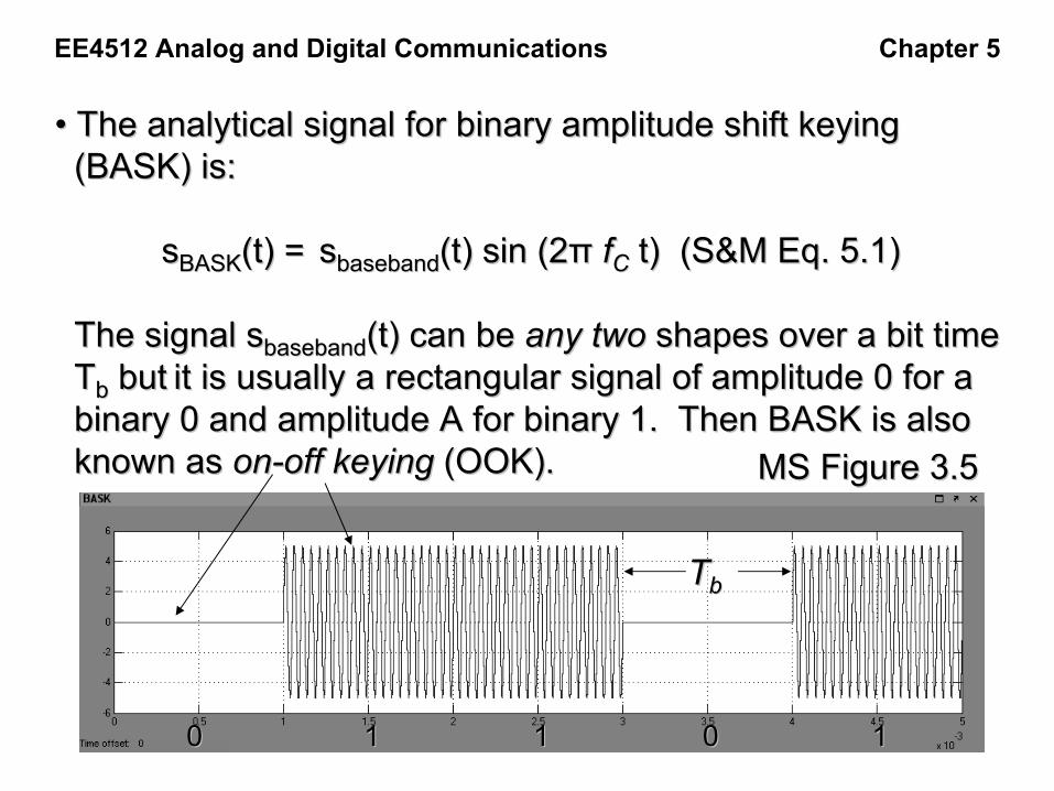
•• The analytical signal for binary amplitude shift keying The analytical signal for binary amplitude shift keying (BASK) is:(BASK) is:
ssBASKBASK(t(t) =) = ssbasebandbaseband(t(t) sin (2) sin (2ππ ffCC t)t) (S&M Eq. 5.1)(S&M Eq. 5.1)
The signal The signal ssbasebandbaseband(t(t) can be ) can be any twoany two shapes over a bit time shapes over a bit time TTbb butbut it is usually a rectangular signal of amplitude 0 for a it is usually a rectangular signal of amplitude 0 for a binary 0 and amplitude A for binary 1. Then BASK is also binary 0 and amplitude A for binary 1. Then BASK is also known as known as onon--off keyingoff keying (OOK).(OOK).
TTbb
0 1 1 0 0 1 1 0 1 1
MS Figure 3.5MS Figure 3.5

EE4512 Analog and Digital Communications Chapter 5
•• The binary amplitude shift keying (BASK) signal can be The binary amplitude shift keying (BASK) signal can be simulated in simulated in SimulinkSimulink..
ssBASKBASK(t(t) = ) = ssbasebandbaseband(t(t) sin 2) sin 2ππ ffCC t (S&M Eq. 5.1)t (S&M Eq. 5.1)
baseband binary PAM signal 0,baseband binary PAM signal 0,1 V, 1 V, rrbb = 1 kb/sec= 1 kb/sec
Sinusoidal carrier Sinusoidal carrier ffCC = 20 kHz, A= 20 kHz, Acc = 5 V= 5 V
MultiplierMultiplierBASK signalBASK signal

EE4512 Analog and Digital Communications Chapter 5
•• A BASK signal is a baseband binary PAM signal multiplied A BASK signal is a baseband binary PAM signal multiplied by a carrier (S&M Figure 5by a carrier (S&M Figure 5--3). 3). Unmodulated sinusoidal carrierUnmodulated sinusoidal carrier
Baseband binary PAM signalBaseband binary PAM signal
BASK signalBASK signal

EE4512 Analog and Digital Communications Chapter 5
•• The unipolar binary PAM signal can be decomposed into a The unipolar binary PAM signal can be decomposed into a polar PAM signal and DC level (S&M Figure 5polar PAM signal and DC level (S&M Figure 5--4). 4). Unipolar binary PAM signalUnipolar binary PAM signal
Polar binary PAM signalPolar binary PAM signal
DC levelDC level
0 0 →→ 1 V1 V
±± 0.5 V0.5 V
0.5 V0.5 V

EE4512 Analog and Digital Communications Chapter 5
•• The spectrum of the BASK signal is (S&M Eq. 5.2):The spectrum of the BASK signal is (S&M Eq. 5.2):
SSBASKBASK(f(f) = ) = FF( ( ssASKASK(t(t) )) ) == FF( ( ssbasebandbaseband(t(t) sin (2) sin (2ππ ffCC t) )t) )SSBASKBASK(f(f) = 1/2 j) = 1/2 j (Sbaseband(f – fC) + Sbaseband(f + fC) )
The analytical signal for the baseband binary PAM signal is:The analytical signal for the baseband binary PAM signal is:
ssbasebandbaseband(t(t) = ) = ssPAMPAM(t(t) + A/2 ) + A/2 (S&M Eq. 5.3)(S&M Eq. 5.3)SSbasebandbaseband(f(f) = ) = SSPAMPAM(f(f) + A/2 ) + A/2 δδ(f) (f) (S&M Eq. 5.4)(S&M Eq. 5.4)
Therefore by substitution (S&M Eq. 5.5):Therefore by substitution (S&M Eq. 5.5):
SSBASKBASK(f(f) = 1/ 2j ( ) = 1/ 2j ( SSPAMPAM(f(f –– ffCC) + A/2 ) + A/2 δδ(f (f –– ffCC) ) –– SSPAMPAM(f(f + + ffCC) ) –– A/2 A/2 δδ(f + (f + ffCC) )) )

EE4512 Analog and Digital Communications Chapter 5
•• TheThe bibi--sided sided power spectral density PSD of the BASK power spectral density PSD of the BASK signal is (S&M Eq. 5.7):signal is (S&M Eq. 5.7):
GGBASKBASK(f(f) = 1/4 ) = 1/4 GGPAMPAM(f(f –– ffCC) + 1/4 ) + 1/4 GGPAMPAM(f(f + + ffCC))+ A+ A22/16 /16 δδ(f (f –– ffCC) + A) + A22/16 /16 δδ(f + (f + ffCC))
For a rectangular polar PAM signal (For a rectangular polar PAM signal (±± A):A):
GGPAMPAM(f(f) = (A/2)) = (A/2)2 2 / r/ rb b sincsinc22 ((ππ f / f / rrbb)) (S&M Eq. 5.8)(S&M Eq. 5.8)
MS Figure 3.7MS Figure 3.7

EE4512 Analog and Digital Communications Chapter 5
•• The The singlesingle--sidedsided power spectral density PSD of the BASK power spectral density PSD of the BASK signal is:signal is:
GGPAMPAM(f(f) = (A/2)) = (A/2)22 / r/ rb b sincsinc22 ((ππ f / rf / rbb))GGBASKBASK(f(f) = 1/2 ) = 1/2 GGPAMPAM(f(f + + ffCC) + A) + A22/8 /8 δδ(f + (f + ffCC))
Carrier 20 kHzCarrier 20 kHz
sincsinc22rrbb = 1 kHz= 1 kHz
MS Figure 3.7MS Figure 3.7
1 kHz1 kHz

EE4512 Analog and Digital Communications Chapter 5
•• The The bandwidthbandwidth of a BASK signal as a percentage of total of a BASK signal as a percentage of total power is power is double double that for the same bit rate that for the same bit rate rrbb = 1/= 1/TTbb binary binary rectangular PAM (MS Table 2.1 p. 22)rectangular PAM (MS Table 2.1 p. 22)
(MS Table 3.1 p. 91).(MS Table 3.1 p. 91).Bandwidth (Hz) Percentage of Total PowerBandwidth (Hz) Percentage of Total Power
2/2/TTbb 90%90%3/3/TTbb 93%93%4/4/TTbb 95%95%6/6/TTbb 96.5%96.5%8/8/TTbb 97.5%97.5%10/10/TTbb 98%98%

EE4512 Analog and Digital Communications Chapter 5
Chapter 5Chapter 5
Digital Bandpass ModulationDigital Bandpass Modulationand Demodulationand DemodulationTechniquesTechniques•• Binary Phase Shift KeyingBinary Phase Shift Keying
•• Pages 219Pages 219--225225

EE4512 Analog and Digital Communications Chapter 5
•• The analytical signal for binary phase shift keying The analytical signal for binary phase shift keying (BPSK) is:(BPSK) is:
ssBPSKBPSK(t(t) =) = ssbasebandbaseband sin (2sin (2ππ ffCC t + t + θθ) (S&M Eq. 5.11)) (S&M Eq. 5.11)ssbasebandbaseband(t(t) = + A b) = + A bii = 1 = 1 ssbasebandbaseband(t(t) = ) = –– A bA bii = 0 = 0
00°°+180+180°° +180+180°°
0 0 1 1 0 0 1 1 00
MS Figure 3.13MS Figure 3.13TTbb
00°°00°°

EE4512 Analog and Digital Communications Chapter 5
•• The BPSK signal initial phase The BPSK signal initial phase θθ = 0= 0°°, +A is a phase shift = , +A is a phase shift = 00°° and and ––A is a phase shift = +180A is a phase shift = +180°°
ssBPSKBPSK(t(t) =) = ssbasebandbaseband sin (2sin (2ππ ffCC t) (S&M Eq. 5.11)t) (S&M Eq. 5.11)ssbasebandbaseband(t(t) = + A b) = + A bii = 1 = 1 ssbasebandbaseband(t(t) = ) = –– A bA bii = 0 = 0
00°°+180+180°° +180+180°°
0 0 1 1 0 0 1 1 00
MS Figure 3.13MS Figure 3.13TTbb
00°°00°°

EE4512 Analog and Digital Communications Chapter 5
•• The binary phase shift keying (BPSK) signal can be The binary phase shift keying (BPSK) signal can be simulated in simulated in SimulinkSimulink..
baseband binary PAM signal baseband binary PAM signal 0,1 V, 0,1 V, rrbb = 1 kb/sec= 1 kb/sec
PM modulatorPM modulator
BPSK BPSK signalsignal
Fig312.mdlFig312.mdl

EE4512 Analog and Digital Communications Chapter 5
•• The Phase ModulatorThe Phase Modulatorblock is in theblock is in theModulation,Modulation,CommunicationCommunicationBlocksetBlockset but as anbut as ananalog analog passbandpassbandmodulatormodulator not not a digitala digitalbasebandbaseband modulator.modulator.

EE4512 Analog and Digital Communications Chapter 5
•• The Phase Modulator block has the parameters of a The Phase Modulator block has the parameters of a carrier frequencycarrier frequency ffCC in Hz, in Hz, initial phaseinitial phase in radians and the in radians and the phase deviation constantphase deviation constant in radians per volt (in radians per volt (radrad / V)./ V).
ffCC = 20 kHz= 20 kHzinitial phase initial phase φφoo = = ππphase deviation phase deviation kkpp = = ππ / V/ V

EE4512 Analog and Digital Communications Chapter 5
•• The Random Integer Generator outputs 0,1 V and with a The Random Integer Generator outputs 0,1 V and with a initial phase = initial phase = ππ and a and a phase deviation constant = phase deviation constant = ππ/V, /V, the phase output the phase output φφ of the BPSK signal is:of the BPSK signal is:
bbii = 0 = 0 φφ = = ππ + 0(+ 0(ππ/V) = /V) = ππbbii = 1 = 1 φφ = = ππ + 1(+ 1(ππ/V) = 2/V) = 2ππ = 0 = 0

EE4512 Analog and Digital Communications Chapter 5
•• The spectrum of the BPSK signal is (S&M Eq. 5.13):The spectrum of the BPSK signal is (S&M Eq. 5.13):
SSBPSKBPSK(f(f) = ) = FF( ( ssPSKPSK(t(t) )) ) == FF(s(sbasebandbaseband(t(t) sin 2) sin 2ππ ffCC t)t)SSBPSKBPSK(f(f) = 1/2 j) = 1/2 j (Sbaseband(f – fc) + Sbaseband(f + fC) )
The analytical signal for the baseband binary PAM signal is:The analytical signal for the baseband binary PAM signal is:
ssbasebandbaseband(t(t) = ) = ssPAMPAM(t(t) ) (S&M Eq. 5.12)(S&M Eq. 5.12)SSbasebandbaseband(f(f) = ) = SSPAMPAM(f(f))
Note that there is Note that there is no DC levelno DC level in in ssPAMPAM(t(t) and therefore by ) and therefore by substitution:substitution:
SSBPSKBPSK(f(f) = 1/ 2j ( ) = 1/ 2j ( SSPAMPAM(f(f –– ffCC) ) –– SSPAMPAM(f(f + + ffCC) )) )

EE4512 Analog and Digital Communications Chapter 5
•• TheThe bibi--sided sided power spectral density PSD of the BPSK power spectral density PSD of the BPSK signal is (S&M Eq. 5.13)signal is (S&M Eq. 5.13)
GGBPSKBPSK(f) = 1/4 (f) = 1/4 GGPAMPAM(f(f –– ffCC) + 1/4 ) + 1/4 GGPAMPAM(f(f + + ffCC))
For a rectangular polar PAM signal (For a rectangular polar PAM signal (±± A):A):
GGPAMPAM(f(f) = A) = A2 2 / / rrbb sincsinc22 ((ππ f / f / rrbb) (S&M Eq. 5.8 modified)) (S&M Eq. 5.8 modified)
MS Figure 3.14MS Figure 3.14

EE4512 Analog and Digital Communications Chapter 5
•• The The singlesingle--sidedsided power spectral density PSD of the BPSK power spectral density PSD of the BPSK signal is:signal is:
GGBPSKBPSK(f) = 1/2 (f) = 1/2 GGPAMPAM(f(f + f+ fCC))GGPAMPAM(f(f) = A) = A2 2 / r/ rb b sincsinc22 ((ππ f / rf / rbb))
No carrierNo carrier
sincsinc22rrbb = 1 kHz= 1 kHz
MS Figure 3.14MS Figure 3.14

EE4512 Analog and Digital Communications Chapter 5
•• The The bandwidthbandwidth of a BPSK signal as a percentage of total of a BPSK signal as a percentage of total power is power is double double that for the same bit rate that for the same bit rate rrbb = 1/= 1/TTbb binary binary rectangular PAM (MS Table 2.1 p. 22) and the same as rectangular PAM (MS Table 2.1 p. 22) and the same as BASK (MS Table 3.1 p. 91)BASK (MS Table 3.1 p. 91)
(MS Tabl(MS Table 3.5 p. 100) e 3.5 p. 100) Bandwidth (Hz) Percentage of Total PowerBandwidth (Hz) Percentage of Total Power
2/2/TTbb 90%90%3/3/TTbb 93%93%4/4/TTbb 95%95%6/6/TTbb 96.5%96.5%8/8/TTbb 97.5%97.5%10/10/TTbb 98%98%

EE4512 Analog and Digital Communications Chapter 5
Chapter 5Chapter 5
Digital Bandpass ModulationDigital Bandpass Modulationand Demodulationand DemodulationTechniquesTechniques•• Binary Frequency Shift KeyingBinary Frequency Shift Keying
•• Pages 219Pages 219--225225

EE4512 Analog and Digital Communications Chapter 5
•• The analytical signal for binary frequency shift keying The analytical signal for binary frequency shift keying (BFSK) is:(BFSK) is:
ssBFSKBFSK(t(t) =) = A sin (2A sin (2ππ ((ffCC + + ∆∆ff) t + ) t + θθ) if b) if bii = 1= 1ssBFSKBFSK(t(t) = A sin (2) = A sin (2ππ ((ffCC –– ∆∆ff) t + ) t + θθ) if b) if bii = 0= 0
ffcc + + ∆∆ffffcc –– ∆∆ff ffcc –– ∆∆ff
0 1 1 0 0 1 1 0 00
TTbbffcc + + ∆∆ffffcc –– ∆∆ff MS Figure 3.9MS Figure 3.9

EE4512 Analog and Digital Communications Chapter 5
•• The BFSK signal initial phase The BFSK signal initial phase θθ = 0= 0°°
ssBFSKBFSK(t(t) =) = A sin (2A sin (2ππ ((ffCC + + ∆∆ff) t) if b) t) if bii = 1= 1ssBFSKBFSK(t(t) = A sin (2) = A sin (2ππ ((ffCC –– ∆∆ff) t) if b) t) if bii = 0= 0
ffcc + + ∆∆ffffcc –– ∆∆ff ffcc –– ∆∆ff
0 1 1 0 0 1 1 0 00
TTbbffcc + + ∆∆ffffcc –– ∆∆ff MS Figure 3.9MS Figure 3.9

EE4512 Analog and Digital Communications Chapter 5
•• The binary frequency shift keying (BFSK) signal can be The binary frequency shift keying (BFSK) signal can be simulated in simulated in SimulinkSimulink..
baseband binary PAM signal baseband binary PAM signal 0,1 V, 0,1 V, rrbb = 1 kb/sec= 1 kb/sec
FM ModulatorFM Modulator
BFSK BFSK signalsignal
Fig38.mdlFig38.mdl
EE4512 Analog and Digital Communications Chapter 5
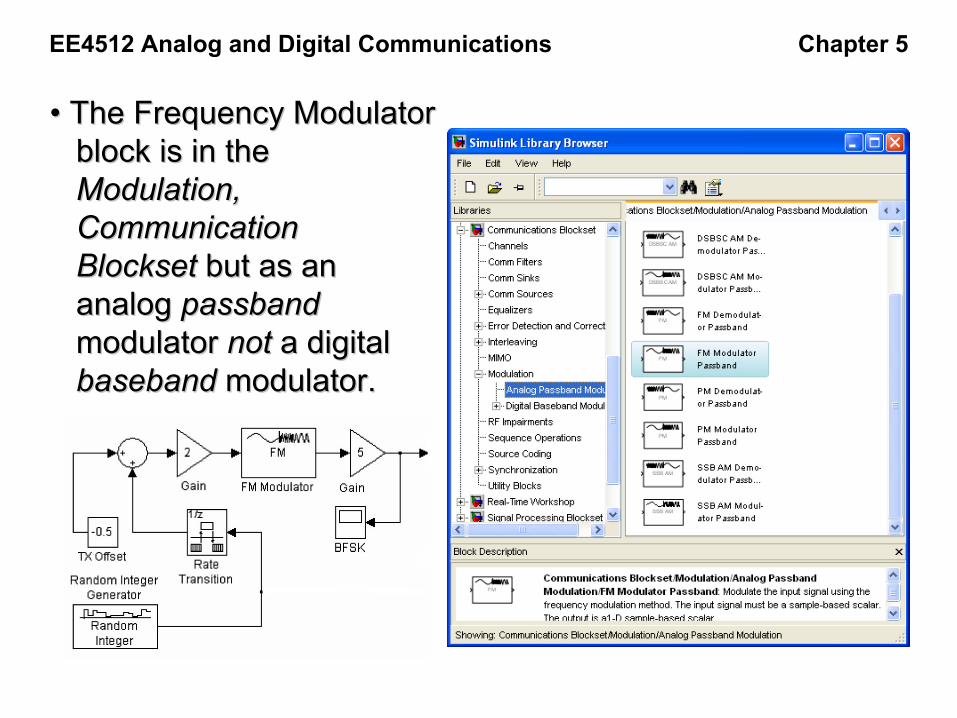
•• The Frequency ModulatorThe Frequency Modulatorblock is in theblock is in theModulation,Modulation,CommunicationCommunicationBlocksetBlockset but as anbut as ananalog analog passbandpassbandmodulatormodulator not not a digitala digitalbasebandbaseband modulator.modulator.

EE4512 Analog and Digital Communications Chapter 5
•• The Frequency Modulator block has the parameters of a The Frequency Modulator block has the parameters of a carrier frequencycarrier frequency ffCC in Hz, in Hz, initial phaseinitial phase in radians and the in radians and the frequency deviation constantfrequency deviation constant in Hertz per volt (Hz/V).in Hertz per volt (Hz/V).
ffCC = 20 kHz= 20 kHzinitial phase = initial phase = 00frequency deviation =frequency deviation =
20002000

EE4512 Analog and Digital Communications Chapter 5
•• The Random Integer Generator outputs 0,1 V but is offset The Random Integer Generator outputs 0,1 V but is offset to to ±±1 1 and with a initial phase = and with a initial phase = 0 and a 0 and a frequency frequency deviation constant = deviation constant = 20002000 Hz/V, the frequency shift Hz/V, the frequency shift ∆∆ff of of the BFSK signal is:the BFSK signal is:
bbii = 0 d= 0 dii = = ––1 1 ∆∆ff = = 0 0 –– 1(2000 Hz/V) = 1(2000 Hz/V) = ––2000 Hz2000 Hzbbii = 1 d= 1 di i = +1 = +1 ∆∆ff = 0 + 1(2000 Hz/V) = +2000 Hz = 0 + 1(2000 Hz/V) = +2000 Hz

EE4512 Analog and Digital Communications Chapter 5
•• The BFSK signal can be The BFSK signal can be decomposeddecomposed as (S&M Eq. 5.14):as (S&M Eq. 5.14):
ssBFSKBFSK(t(t) =) = ssbaseband1baseband1(t) sin (2(t) sin (2ππ ((ffCC + + ∆∆ff) t + ) t + θθ) +) +ssbaseband2baseband2(t) sin (2(t) sin (2ππ ((ffCC –– ∆∆ff) t + ) t + θθ))
ffcc –– ∆∆ffffcc + + ∆∆ff ffcc –– ∆∆ff ffcc + + ∆∆ff ffcc + + ∆∆ff
1 0 0 1 1 0 0 1 1 1
EE4512 Analog and Digital Communications Chapter 5
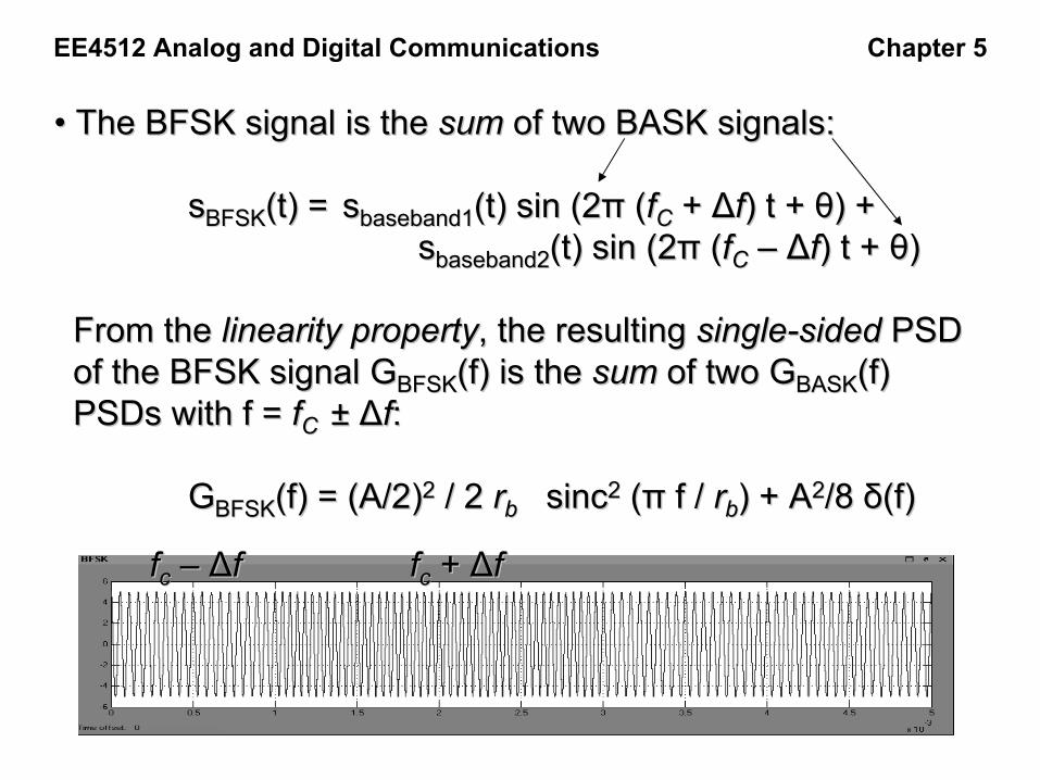
•• The BFSK signal is the The BFSK signal is the sum sum of two BASK signals:of two BASK signals:
ssBFSKBFSK(t(t) =) = ssbaseband1baseband1(t) sin (2(t) sin (2ππ ((ffCC + + ∆∆ff) t + ) t + θθ) +) +ssbaseband2baseband2(t) sin (2(t) sin (2ππ ((ffCC –– ∆∆ff) t + ) t + θθ))
From the From the linearity propertylinearity property, the resulting , the resulting singlesingle--sidedsided PSD PSD of the BFSK signal of the BFSK signal GGBFSKBFSK(f(f) is the ) is the sum sum of two of two GGBASKBASK(f(f) ) PSDs with f = PSDs with f = ffCC ±± ∆∆ff::
GGBFSKBFSK(f(f) = (A/2)) = (A/2)22 / 2 / 2 rrbb sincsinc22 ((ππ f / f / rrbb) + A) + A22/8 /8 δδ(f)(f)
ffcc ++ ∆∆ffffcc –– ∆∆ff

EE4512 Analog and Digital Communications Chapter 5
•• The The singlesingle--sidedsided power spectral density PSD of the BFSK power spectral density PSD of the BFSK signal is:signal is:
GGBFSKBFSK(f(f) = (A/2)) = (A/2)2 2 / 2/ 2rrbb sincsinc22 ((ππ ((ffCC + + ∆∆ff)) / / rrbb) + A) + A22/8 /8 δδ((ffCC + + ∆∆ff))+ (A/2)+ (A/2)22 / 2/ 2rrbb sincsinc22 ((ππ ((ffCC –– ∆∆ff)/ / rrbb) + A) + A22/8 /8 δδ((ffCC –– ∆∆ff))
carrierscarriers
sincsinc22
rrb b = 1 kHz= 1 kHz
MS Figure 3.10MS Figure 3.10
∆∆ff = 2 kHz= 2 kHz

EE4512 Analog and Digital Communications Chapter 5
•• Minimum frequency shift keying (MFSK) for BFSK occurs Minimum frequency shift keying (MFSK) for BFSK occurs when when ∆∆ff = 1/2Tb = rb/2 Hz.
GGBFSKBFSK(f(f) = (A/2)) = (A/2)2 2 / 2/ 2rrbb sincsinc22 ((ππ ((ffCC + + ∆∆ff)) / / rrbb) + A) + A22/8 /8 δδ((ffCC+ + ∆∆ff) ) + (A/2)+ (A/2)22 / 2/ 2rrbb sincsinc22 ((ππ ((ffCC –– ∆∆ff)/ / rrbb) + A) + A22/8 /8 δδ((ffCC –– ∆∆ff))
carrierscarriers
sincsinc22rrb b = 1 kHz= 1 kHz
MS Figure 3.11MS Figure 3.11
∆∆ff = 500 Hz= 500 Hz

EE4512 Analog and Digital Communications Chapter 5
•• This BFSK This BFSK carrier frequency separationcarrier frequency separation 22∆∆f f = 1/= 1/TTbb = = rrbb Hz is Hz is thethe minimum possibleminimum possible because each carrier spectral impulse because each carrier spectral impulse is at the is at the null null of the PSD of the other decomposed BASK of the PSD of the other decomposed BASK signal and thus is called signal and thus is called minimum frequency shift keyingminimum frequency shift keying(MFSK). (MFSK).
MS Figure 3.11MS Figure 3.11
22∆∆ff = 1000 Hz= 1000 Hzsincsinc22
carrierscarriers
rrb b = 1 kHz= 1 kHz

EE4512 Analog and Digital Communications Chapter 5
•• The The bandwidthbandwidth of a BFSK signal as a percentage of total of a BFSK signal as a percentage of total power is power is greatergreater than that of either BASK or BPSK by 2than that of either BASK or BPSK by 2∆∆ffHz for the same bit rate Hz for the same bit rate rrbb = 1/= 1/TTbb (MS Table 3.3 p. 95). (MS Table 3.3 p. 95).
For MFSK 2For MFSK 2∆∆ff = rrbb = 1/= 1/TTbb Hz. Hz.
Bandwidth (Hz) Percentage of Total PowerBandwidth (Hz) Percentage of Total Power
22∆∆f f + + 2/2/TTbb 90%90%22∆∆ff ++ 3/3/TTbb 93%93%22∆∆ff ++ 4/4/TTbb 95%95%22∆∆ff ++ 6/6/TTbb 96.5%96.5%22∆∆f f ++ 8/8/TTbb 97.5%97.5%22∆∆f f ++ 10/10/TTbb 98%98%

EE4512 Analog and Digital Communications Chapter 5
Chapter 5Chapter 5
Digital Bandpass ModulationDigital Bandpass Modulationand Demodulationand DemodulationTechniquesTechniques•• Coherent Demodulation ofCoherent Demodulation ofBandpass SignalsBandpass Signals
•• Pages 225Pages 225--236236
EE4512 Analog and Digital Communications Chapter 5
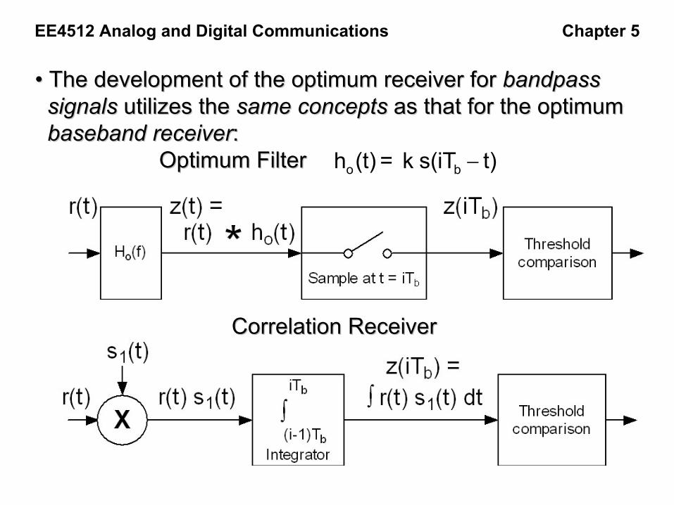
•• The development of the optimum receiver for The development of the optimum receiver for bandpass bandpass signalssignals utilizes the utilizes the same conceptssame concepts as that for the optimum as that for the optimum baseband receiverbaseband receiver::
Optimum FilterOptimum Filter −o bh (t) = k s(iT t)
Correlation ReceiverCorrelation Receiver

EE4512 Analog and Digital Communications Chapter 5
•• The optimum filter The optimum filter HHoo(f(f) and the correlation receiver ) and the correlation receiver are equivalent here also, with sare equivalent here also, with s11(t) = (t) = s(ts(t) for ) for symmetrical symmetrical signalssignals and and r(tr(t) = ) = γγ s(ts(t) + ) + n(tn(t) where ) where γγ is the communication is the communication channel attenuation and channel attenuation and n(tn(t) is AWGN. The energy per bit ) is AWGN. The energy per bit EEbb and the probability of bit error and the probability of bit error PPbb is (S&M p. 226):is (S&M p. 226):
∫ ∫b b
b b
iT iT2 2
(i-1)T (i-1)T
= γ s(t) γ s(t) dt = γ s (t) dtbE
2 = Q bb
o
EPN

EE4512 Analog and Digital Communications Chapter 5
•• The matched filter or correlation receiver is a The matched filter or correlation receiver is a coherent coherent demodulationdemodulation process for bandpass signals because not process for bandpass signals because not only is bit time (only is bit time (TTbb) as for baseband signals required but ) as for baseband signals required but carrier carrier synchronizationsynchronization is also needed. Carrier is also needed. Carrier synchronization requires an estimate of the synchronization requires an estimate of the transmitted transmitted frequencyfrequency ((ffCC) and the ) and the arrival phasearrival phase at the receiver (at the receiver (θθ):):
1s (t) = sin(2π t + θ)C f

EE4512 Analog and Digital Communications Chapter 5
•• BPSK signals are symmetrical with:BPSK signals are symmetrical with:ss1T1T(t) = (t) = –– ss2T2T(t) = A sin(2(t) = A sin(2ππ ffc c t) S&M t) S&M EqsEqs. 5.15. 5.15--5.195.19
[ ]
[ ]−
∫
∫
i2
(i-1)
i 2 22 2
(i-1)
= ± A γ sin (2π t) dt
γ Aγ A= 1 cos (4π t) dt = 2 2
b
b
b
b
T
b, BPSK CT
Tb
b, BPSK CT
E f
TE f
2 2 2 γ A = Q = Qb bb, BPSK
o o
E TPN N

EE4512 Analog and Digital Communications Chapter 5
•• For this analysis of For this analysis of EEb, PSKb, PSK for BPSK signals it is assumed for BPSK signals it is assumed that the transmitter produces an that the transmitter produces an integer numberinteger number of cycles of cycles within one bit period within one bit period TTbb::
[ ]−
−
∫
∫
i2 2
(i-1)
i2 2 2 2
(i-1)
γ A= 1 cos (4π t) dt2
γ A γ A= cos (4π t) dt2 2
b
b
b
b
T
b, BPSK CT
Tb
b, BPSK CT
E f
TE f
00
S&M Eq. 5.17S&M Eq. 5.17

EE4512 Analog and Digital Communications Chapter 5
•• However, even for a nonHowever, even for a non--integer number of cycles within integer number of cycles within one bit period one bit period TTbb if 1 / if 1 / ffCC = = TTCC << << TTbb::
−
∫
∫
i
(i-1)
i2 2 2 2
(i-1)
cos (4π t) dt <<
γ A γ A= cos (4π t) dt2 2
b
b
b
b
T
C bT
Tb
b, BPSK CT
f T
TE f
insignificantinsignificant
S&M Eq. 5.17S&M Eq. 5.17

EE4512 Analog and Digital Communications Chapter 5
•• BPSK signals are symmetrical with:BPSK signals are symmetrical with:ss1T1T(t) = (t) = –– ss2T2T(t) = A sin(2(t) = A sin(2ππ ffc c t) S&M t) S&M EqsEqs. 5.15. 5.15--5.195.19
and sand s11(t) = sin (2(t) = sin (2ππ ffc c t)t)
∫i
i i 1(i-1)
a (i ) = γ s (t) s (t) dt b
b
T
bT
T
= 2 1
opta (i )+ a (i )τ = 0
2b bT T
S&M Eq. 4.67S&M Eq. 4.67
S&M Eq. 4.71S&M Eq. 4.71

EE4512 Analog and Digital Communications Chapter 5
•• BPSK signals are symmetrical with:BPSK signals are symmetrical with:ss1T1T(t) = (t) = –– ss2T2T(t) = A sin(2(t) = A sin(2ππ ffc c t) S&M t) S&M EqsEqs. 5.15. 5.15--5.195.19
=optτ 0
S&M Figure 4S&M Figure 4--1616

EE4512 Analog and Digital Communications Chapter 5
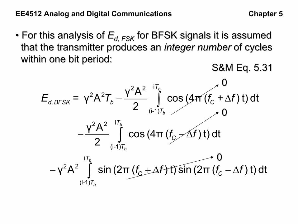
•• For this analysis of For this analysis of EEd, ASKd, ASK for BASK signals it is assumed for BASK signals it is assumed that the transmitter produces an that the transmitter produces an integer numberinteger number of cycles of cycles within one bit period:within one bit period:
[ ]−
−
∫
∫
i2 2
(i-1)
i2 2 2 2
(i-1)
γ A= 1 cos (4π t) dt2
γ A γ A= cos (4π t) dt2 2
b
b
b
b
T
d, BASK CT
Tb
d, BASK CT
E f
TE f
00
S&M Eq. 5.27S&M Eq. 5.27

EE4512 Analog and Digital Communications Chapter 5
•• BASK OOK signals are BASK OOK signals are not not symmetrical with:symmetrical with:ss1T1T(t) = A sin(2(t) = A sin(2ππ ffcctt) ) ss2T2T(t) = 0(t) = 0 S&M S&M EqsEqs. 5.22, 5.23. 5.22, 5.23
and sand s11(t) = sin(2(t) = sin(2ππ ffcctt) s) s22(t) = 0(t) = 0
[ ]−∫
∫
i
i i 1 2(i-1)
i2
1 1 2(i-1)
a (i ) = γ s (t) s (t) s (t) dt
γ A a (i ) = γ A s (t) dt = a (i ) = 0 2
b
b
b
b
T
bT
Tb
b bT
T
TT T
S&M Eq. 5.24S&M Eq. 5.24--5.265.26
2 1opt
a (i )+ a (i ) γ A τ = = 2 4
b b bT T T

EE4512 Analog and Digital Communications Chapter 5
•• BASK signals BASK signals in generalin general may may notnot be symmetrical with:be symmetrical with:ss1T1T(t) = A(t) = A11 sin(2sin(2ππ ffc c t) st) s2T2T(t) = A(t) = A22 sin(2sin(2ππ ffc c t)t)
and sand s11(t) (t) –– ss22(t) = sin (2(t) = sin (2ππ ffc c t) where the amplitude is arbitrary.t) where the amplitude is arbitrary.
( ) = = 1 22 1
opt
γ A + Aa (i )+ a (i )τ2 4
bb b TT T
[ ]−∫
∫
i
i i 1 2(i-1)
i2 i
i i 1(i-1)
a (i ) = γ s (t) s (t) s (t) dt
γ Aa (i ) = γ A s (t) dt = 2
b
b
b
b
T
bT
Tb
bT
T
TT
S&M Eq. 4.67S&M Eq. 4.67
S&M Eq. 4.71S&M Eq. 4.71

EE4512 Analog and Digital Communications Chapter 5
•• BFSK signals are BFSK signals are notnot symmetrical with:symmetrical with:ssTT(t(t) = A sin(2) = A sin(2ππ ((ffcc ±± ∆∆ff)) t) S&M Eq. 5.30t) S&M Eq. 5.30
[ ]
if and
∆ − − ∆
∆ − ∆
∫b
b
iT2
(i-1)T
2 2b 1 2
= A γ (sin (2π + ) t sin (2π ) t )) dt
= γ A T + = n / = n /
d, BFSK C C
d, BFSK C b C b
E f f f f
E f f T f f T
=
2 2 γ A = Q Q2 2
d, FSK bb, BFSK
o o
E TPN N
S&M Eq. 5.31S&M Eq. 5.31S&M Eq. 5.32S&M Eq. 5.32
EE4512 Analog and Digital Communications Chapter 5
•• For this analysis of For this analysis of EEd, FSKd, FSK for BFSK signals it is assumed for BFSK signals it is assumed that the transmitter produces an that the transmitter produces an integer numberinteger number of cycles of cycles within one bit period:within one bit period:
− ∆
− − ∆
− + ∆ − ∆
∫
∫
∫
i2 22 2
(i-1)
i2 2
(i-1)
i2 2
(i-1)
γ A= γ A cos (4π ( + ) t) dt2
γ A cos (4π ( ) t) dt2
γ A sin (2π ( ) t) sin (2π ( ) t) dt
b
b
b
b
b
b
T
d, BFSK b CT
T
CT
T
C CT
E T f f
f f
f f f f
00S&M Eq. 5.31S&M Eq. 5.31
00
00

EE4512 Analog and Digital Communications Chapter 5
•• BFSK signals are BFSK signals are notnot symmetrical with:symmetrical with:ssTT(t(t) = A sin(2) = A sin(2ππ ((ffc c ±± ∆∆ff)) t) S&M Eq. 5.30t) S&M Eq. 5.30
and sand s11(t) (t) –– ss22(t) = sin(2(t) = sin(2ππ ((ffcc + + ∆∆ff) t)) t) – sin(2sin(2ππ ((ffcc –– ∆∆ff) t)) t)
S&M Eq. 5.31S&M Eq. 5.31
S&M Eq. 5.33S&M Eq. 5.33
[ ]−∫
∫
i
i i 1 2(i-1)
i2 i
i i i(i-1)
a (i ) = γ s (t) s (t) s (t) dt
γ Aa (i ) = γ A s (t) dt = 2
b
b
b
b
T
bT
Tb
bT
T
TT
( )
if
− 1 22 1opt
1 2
γ A Aa (i )+ a (i )τ = = = 02 4
A = A
bb b TT T

EE4512 Analog and Digital Communications Chapter 5
•• A comparison of coherent BPSK, BFSK and BASKA comparison of coherent BPSK, BFSK and BASKillustrates the functional differences, but BFSK and BASK illustrates the functional differences, but BFSK and BASK uses uses EEdd and not and not EEbb::
2 2 2 γ A = Q = Qb bb, BPSK
o o
E TPN N
2 2γ A= 2
bb, BPSK
TE
2 2 γ A = Q = Q2 2
d, FSK bb, BFSK
o o
E TPN N
2 2= γ Ad, BFSK bE T
2 2 γ A = Q = Q2 4
d, ASK bb, BASK
o o
E TPN N
2 2γ A= 2
bd, BASK
TE

EE4512 Analog and Digital Communications Chapter 5
•• The normalized The normalized EEb, FSKb, FSK = = EEb, PSKb, PSK = = γγ2 2 AA2 2 TTbb / 2 / 2 (S&M Eq. (S&M Eq. 5.24) and 5.24) and EEb, ASKb, ASK = = γγ22 AA2 2 TTbb / 4/ 4 (S&M Eq. 5.36) so that:(S&M Eq. 5.36) so that:
Thus there are Thus there are no practical advantagesno practical advantages for either coherent for either coherent BFSK or BASK and BPSK is preferred (S&M p. 236).BFSK or BASK and BPSK is preferred (S&M p. 236).
2 2 2 γ A = Q = Qb, PSK bb, BPSK
o o
E TPN N
2 2γ A= 2
bb, BPSK
TE
2 2 γ A = Q = Q2
b, FSK bb, BFSK
o o
E TPN N
2 2γ A= 2
bb, BFSK
TE
2 2 γ A = Q = Q4
b, ASK bb, BASK
o o
E TPN N
2 2γ A= 4
bb, BASK
TE

EE4512 Analog and Digital Communications Chapter 5
•• For the same For the same PPbb BPSK uses the least amount of energy, BPSK uses the least amount of energy, BFSK requires twice as much and BASK four times as much BFSK requires twice as much and BASK four times as much energy:energy:
2 2 2 γ A = Q = Qb, PSK bb, BPSK
o o
E TPN N
2 2 γ A = Q = Q2
b, FSK bb, BFSK
o o
E TPN N
2 2 γ A = Q = Q4
b, ASK bb, BASK
o o
E TPN N
Argument of Argument of Q should be Q should be as as largelarge as as possible to possible to minimize minimize PPbb
EE4512 Analog and Digital Communications Chapter 5
Chapter 3Chapter 3
Bandpass Modulation and Bandpass Modulation and DemodulationDemodulation•• Optimum Bandpass Receiver:Optimum Bandpass Receiver:The Correlation ReceiverThe Correlation Receiver
•• Pages 81Pages 81--8585

EE4512 Analog and Digital Communications Chapter 5
•• The matched filter orThe matched filter orcorrelation receivercorrelation receiverfor for bandpass bandpass symmetricalsymmetricalsignals signals can becan besimulated insimulated inSimulink:Simulink:
MS Figure 3.1MS Figure 3.1

EE4512 Analog and Digital Communications Chapter 5
•• The matched filter orThe matched filter orcorrelation receivercorrelation receiverfor for bandpass bandpass asymmetricalasymmetricalsignals signals can alsocan alsobe simulatedbe simulatedinin Simulink:Simulink:
MS Figure 3.2MS Figure 3.2

EE4512 Analog and Digital Communications Chapter 5
•• The The alternatealternate butbutuniversal universal structurestructurewhich can be usedwhich can be usedfor both asymmetricfor both asymmetricor symmetric binaryor symmetric binarybandpass signals canbandpass signals canbe simulated inbe simulated inSimulink:Simulink: MS Figure 3.3MS Figure 3.3

EE4512 Analog and Digital Communications Chapter 5
Chapter 3Chapter 3
Bandpass Modulation and Bandpass Modulation and DemodulationDemodulation•• Binary Amplitude Shift KeyingBinary Amplitude Shift Keying
•• Pages 86Pages 86--9292

EE4512 Analog and Digital Communications Chapter 5
•• Binary ASK (OOK) coherent digital communication system Binary ASK (OOK) coherent digital communication system with BER analysis:with BER analysis:
MS Figure 3.4MS Figure 3.4
ThresholdThreshold

EE4512 Analog and Digital Communications Chapter 4
•• The BER and The BER and PPbb comparison (MS Table 3.2, p. 91): comparison (MS Table 3.2, p. 91):
Table 3.2Table 3.2 Observed BER and Theoretical Observed BER and Theoretical PPbb as a as a Function of Function of EEd d / N/ Noo in a Binary ASK Digital in a Binary ASK Digital Communication System with Optimum ReceiverCommunication System with Optimum Receiver
EEd d / / NNoo dBdB BERBER PPbb∞∞ 00 001212 2.9 2.9 ×× 1010--33 2.53 2.53 ×× 1010--33
1010 1.12 1.12 ×× 1010--22 1.25 1.25 ×× 1010--22
88 3.46 3.46 ×× 1010--22 3.75 3.75 ×× 1010--22
66 7.65 7.65 ×× 1010--22 7.93 7.93 ×× 1010--22
44 1.335 1.335 ×× 1010--11 1.318 1.318 ×× 1010--11
22 1.863 1.863 ×× 1010--11 1.872 1.872 ×× 1010--11
00 2.387 2.387 ×× 1010--11 2.394 2.394 ×× 1010--11

EE4512 Analog and Digital Communications Chapter 5
Chapter 3Chapter 3
Bandpass Modulation and Bandpass Modulation and DemodulationDemodulation•• Binary Phase Shift KeyingBinary Phase Shift Keying
•• Pages 98Pages 98--103103

EE4512 Analog and Digital Communications Chapter 5
•• Binary PSK coherent digital communication system with Binary PSK coherent digital communication system with BER analysis:BER analysis:
MS Figure 3.12MS Figure 3.12

EE4512 Analog and Digital Communications Chapter 4
•• The BER and The BER and PPbb comparison (SVU Table 3.5, p. 167): comparison (SVU Table 3.5, p. 167):
Table 3.5Table 3.5 Observed BER and Theoretical Observed BER and Theoretical PPbb as a as a Function of Function of EEb b / N/ Noo in a Binary PSK Digital in a Binary PSK Digital Communication System with Optimum ReceiverCommunication System with Optimum Receiver
EEb b / / NNoo dBdB BERBER PPbb∞∞ 00 001010 00 4.05 4.05 ×× 1010--66
88 1 1 ×× 1010--44 2.06 2.06 ×× 1010--44
66 2.5 2.5 ×× 1010--44 2.41 2.41 ×× 1010--33
44 1.31 1.31 ×× 1010--22 1.25 1.25 ×× 1010--22
22 3.35 3.35 ×× 1010--22 3.75 3.75 ×× 1010--22
00 8.19 8.19 ×× 1010--22 7.93 7.93 ×× 1010--22

EE4512 Analog and Digital Communications Chapter 5
Chapter 3Chapter 3
Bandpass Modulation and Bandpass Modulation and DemodulationDemodulation•• Binary Frequency Shift KeyingBinary Frequency Shift Keying
•• Pages 92Pages 92--9898

EE4512 Analog and Digital Communications Chapter 5
•• Binary FSK coherent digital communication system with Binary FSK coherent digital communication system with BER analysis:BER analysis:
MS Figure 3.9MS Figure 3.9
ffCC++∆∆ff
ffCC––∆∆ff

EE4512 Analog and Digital Communications Chapter 5
•• The BER and PThe BER and Pbb comparison (MS Table 3.4, p. 98): comparison (MS Table 3.4, p. 98):
Table 3.4Table 3.4 Observed BER and Theoretical Observed BER and Theoretical PPbb as a as a Function of Function of EEd d / N/ Noo in a Binary FSK (MFSK) Digital in a Binary FSK (MFSK) Digital Communication System with Optimum ReceiverCommunication System with Optimum Receiver
EEdd//NNoo dBdB BERBER PPbb∞∞ 00 001212 2.5 2.5 ×× 1010--33 2.5 2.5 ×× 1010--33
1010 1.29 1.29 ×× 1010--22 1.25 1.25 ×× 1010--22
88 3.50 3.50 ×× 1010--22 3.75 3.75 ×× 1010--22
66 8.04 8.04 ×× 1010--22 7.93 7.93 ×× 1010--22
44 1.352 1.352 ×× 1010--11 1.314 1.314 ×× 1010--11
22 1.833 1.833 ×× 1010--11 1.872 1.872 ×× 1010--11
00 2.456 2.456 ×× 1010--11 2.393 2.393 ×× 1010--11

EE4512 Analog and Digital Communications Chapter 5
•• The BER and PThe BER and Pbb performance comparison for BASK, performance comparison for BASK, BPSK and BFSK (MFSK): BPSK and BFSK (MFSK):
EEd d / / NNoo dBdB BERBER PPbb1010 1.12 1.12 ×× 1010--22 1.25 1.25 ×× 1010--2 2 BASKBASK88 3.46 3.46 ×× 1010--22 3.75 3.75 ×× 1010--22
EEb b / / NNoo dBdB BERBER PPbb1010 00 4.05 4.05 ×× 1010--6 6 BPSKBPSK88 1 1 ×× 1010--44 2.06 2.06 ×× 1010--44
EEd d / / NNoo dBdB BERBER PPbb1010 1.29 1.29 ×× 1010--22 1.25 1.25 ×× 1010--2 2 BFSKBFSK88 3.50 3.50 ×× 1010--22 3.75 3.75 ×× 1010--22

EE4512 Analog and Digital Communications Chapter 5
•• BER and PBER and Pbb comparison using comparison using EEbb with with EEbb, , ASKASK = = γγ22 AA22 TTbb2 2 / 4/ 4
and thus reduced by 10 log (0.5) and thus reduced by 10 log (0.5) ≈≈ ––3 dB or3 dB or::
BASK performs better than BFSK but BPSK is the best. BASK performs better than BFSK but BPSK is the best.
EEb b / / NNoo dBdB BERBER PPbb77 1.12 1.12 ×× 1010--22 1.25 1.25 ×× 1010--2 2 BASKBASK55 3.46 3.46 ×× 1010--22 3.75 3.75 ×× 1010--22
EEb b / / NNoo dBdB BERBER PPbb1010 00 4.05 4.05 ×× 1010--6 6 BPSKBPSK88 1 1 ×× 1010--44 2.06 2.06 ×× 1010--44
EEb b / / NNoo dBdB BERBER PPbb1010 1.29 1.29 ×× 1010--22 1.25 1.25 ×× 1010--2 2 BFSKBFSK88 3.50 3.50 ×× 1010--22 3.75 3.75 ×× 1010--22
EE4512 Analog and Digital Communications Chapter 5
Chapter 5Chapter 5
Digital Bandpass ModulationDigital Bandpass Modulationand Demodulationand DemodulationTechniquesTechniques•• Differential (Noncoherent) PhaseDifferential (Noncoherent) PhaseShift KeyingShift Keying
•• Pages 267Pages 267--271271

EE4512 Analog and Digital Communications Chapter 5
•• Differential (noncoherent) phase shift keying (DPSK) is Differential (noncoherent) phase shift keying (DPSK) is demodulated by using the received signal to derive the demodulated by using the received signal to derive the reference signal. The DPSK reference signal. The DPSK protocolprotocol is:is:
Binary 1Binary 1: Transmit the carrier signal with the : Transmit the carrier signal with the same phasesame phaseas used for the previous bit.as used for the previous bit.
Binary 0Binary 0: Transmit the carrier signal with its : Transmit the carrier signal with its phase shifted phase shifted by 180by 180°° relative to the previous bit. relative to the previous bit.

EE4512 Analog and Digital Communications Chapter 5
•• The oneThe one--bit delayed reference signal rbit delayed reference signal rii--11(t) is derived from (t) is derived from the received signal the received signal rrii(t(t) and if the carrier frequency ) and if the carrier frequency ffCC is an is an integral multiple of the bit rate integral multiple of the bit rate rrbb::
The output of the integrator for a binary 0 and binary 1 The output of the integrator for a binary 0 and binary 1 then is then is z(iz(iTTbb) = ) = ±± γγ22 AA22 TTbb / 2 (S&M / 2 (S&M EqsEqs. 5.91 and 5.93). 5.91 and 5.93)
−
−
−i 1
i 1
r (t) = γ A sin (2π (t ) + θ)r (t) = γ A sin (2π t + θ)
C b
C
f Tf
S&M S&M EqsEqs..5.88 and 5.895.88 and 5.89

EE4512 Analog and Digital Communications Chapter 5
•• DPSK signals have an equivalent bit interval DPSK signals have an equivalent bit interval TTDPSKDPSK = 2 = 2 TTbb. . The probability of bit error for DPSK signal is different thanThe probability of bit error for DPSK signal is different thanthat for coherent demodulation of symmetric or asymmetric that for coherent demodulation of symmetric or asymmetric signals and is: signals and is:
− −
2 2
1 1= exp = exp 2 2 2
γ A =2
b, DPSKDPSKb, DPSK
o o
bb, DPSK
EEPN N
TE S&M Eq. 5.102S&M Eq. 5.102

EE4512 Analog and Digital Communications Chapter 5
Chapter 3Chapter 3
Bandpass Modulation and Bandpass Modulation and DemodulationDemodulation•• Differential Phase Shift KeyingDifferential Phase Shift Keying
•• Pages 130Pages 130--135135

EE4512 Analog and Digital Communications Chapter 5
•• Binary DPSK Binary DPSK noncoherentnoncoherent digital communication system digital communication system with BER analysis:with BER analysis:
MS Figure 3.33MS Figure 3.33
oneone--bitbitcontinuouscontinuous
delaydelayBPFBPF

EE4512 Analog and Digital Communications Chapter 5
•• Binary DPSK Binary DPSK noncoherentnoncoherent digital communication system digital communication system differential binary encoder differential binary encoder Simulink SubsystemSimulink Subsystem::
MS Figure 3.34MS Figure 3.34
XORXOR
one bitone bitsample delaysample delay

EE4512 Analog and Digital Communications Chapter 5
•• Simulink Logic andSimulink Logic andBit OperationsBit Operationsprovides theprovides theLogical OperatorLogical Operatorblock:block:

EE4512 Analog and Digital Communications Chapter 5
•• Simulink Logical OperatorSimulink Logical Operator blocks can be selected to blocks can be selected to provide multiple input AND, OR, NAND, NOR, XOR, provide multiple input AND, OR, NAND, NOR, XOR, NXOR, and NOT functions:NXOR, and NOT functions:

EE4512 Analog and Digital Communications Chapter 5
•• The The Logic and Bit OperationsLogic and Bit Operationscan be configured as can be configured as scalarscalarBoolean binary (0, 1)Boolean binary (0, 1) ororMM--ary (0, 1ary (0, 1……MM−−1)1) vectorvectorlogic functions. Here scalarlogic functions. Here scalarBoolean binary data is used.Boolean binary data is used.

EE4512 Analog and Digital Communications Chapter 5
•• The XOR logic generates the DPSK The XOR logic generates the DPSK source codingsource coding::
Table 3.16Table 3.16 Input Binary Data Input Binary Data bbii, Differentially Encoded , Differentially Encoded Binary Data Binary Data ddii, and Transmitted Phase , and Transmitted Phase φφii (Radians) for a (Radians) for a DPSK Signal.DPSK Signal.
bbii ddii--11 ddii φφii oneone--bit startupbit startup11 0 0
11 11 11 00 XOR logicXOR logic00 11 00 ππ 0 0 10 0 100 00 11 0 0 0 1 00 1 011 11 11 00 1 0 01 0 000 11 00 ππ 1 1 11 1 100 00 11 0011 11 11 0011 11 11 00

EE4512 Analog and Digital Communications Chapter 5
•• The The Signal ProcessingSignal ProcessingBlocksetBlockset provides theprovides theFilteringFiltering, , Analog FilterAnalog FilterDesignDesign block:block:

EE4512 Analog and Digital Communications Chapter 5
•• The The Signal Processing Signal Processing BlocksetBlockset provides the analog provides the analog bandpass filter (BPF) specified as a 9bandpass filter (BPF) specified as a 9--pole Butterworth pole Butterworth filter with cutoff frequencies of 19 kHz and 21 kHzfilter with cutoff frequencies of 19 kHz and 21 kHz centered centered around the carrier frequency around the carrier frequency ffCC = 20 kHz.= 20 kHz.
rad/s

EE4512 Analog and Digital Communications Chapter 5
•• The Butterworth BPF is used for the The Butterworth BPF is used for the noncoherent receivernoncoherent receiver. . The The coherent receivercoherent receiver uses the uses the integratorintegrator as a as a virtual virtual BPFBPF::
MS Figure 3.12 MS Figure 3.12 PSKPSK
MS Figure 3.33 MS Figure 3.33 DPSKDPSK

EE4512 Analog and Digital Communications Chapter 5
•• The BER and The BER and PPbb comparison (MS Table 3.17, p. 134): comparison (MS Table 3.17, p. 134):
Table 3.17Table 3.17 Observed BER and Theoretical Observed BER and Theoretical PPbb as a as a Function of Function of EEb b / N/ Noo in a Binary DPSK Digital in a Binary DPSK Digital Communication System with Noncoherent Correlation Communication System with Noncoherent Correlation Receiver Receiver
EEb b / / NNoo dBdB BERBER PPbb∞∞ 00 001212 00 ≈≈ 6.6 6.6 ×× 1010--88
1010 2 2 ×× 1010--44 2.3 2.3 ×× 1010--55
88 5.1 5.1 ×× 1010--33 1.8 1.8 ×× 1010--33
66 2.61 2.61 ×× 1010--22 9.3 9.3 ×× 1010--33
44 7.91 7.91 ×× 1010--22 4.06 4.06 ×× 1010--22
22 1.559 1.559 ×× 1010--22 1.025 1.025 ×× 1010--11
00 2.393 2.393 ×× 1010--11 1.839 1.839 ×× 1010--11
Statistical variationStatistical variationdue to small sample due to small sample
sizesize

EE4512 Analog and Digital Communications Chapter 5
•• BER and BER and PPbb comparison between noncoherent, source comparison between noncoherent, source coded DPSK and coherent BPSK:coded DPSK and coherent BPSK:
BPSK performs better than DPSK but requires a coherent BPSK performs better than DPSK but requires a coherent reference signal. DPSK performs nearly as well as BPSK reference signal. DPSK performs nearly as well as BPSK at high SNR. at high SNR.
EEb b / / NNoo dBdB BERBER PPbb1212 00 6.6 6.6 ×× 1010--8 8 DPSKDPSK1010 2 2 ×× 1010--44 2.3 2.3 ×× 1010--55
88 5.1 5.1 ×× 1010--33 1.8 1.8 ×× 1010--33
EEb b / / NNoo dBdB BERBER PPbb1010 00 4.05 4.05 ×× 1010--6 6 BPSKBPSK88 2 2 ×× 1010--44 2.06 2.06 ×× 1010--44
66 2.5 2.5 ×× 1010--33 2.41 2.41 ×× 1010--33

EE4512 Analog and Digital Communications Chapter 5
Chapter 5Chapter 5
Digital Bandpass ModulationDigital Bandpass Modulationand Demodulationand DemodulationTechniquesTechniques•• MM--ary Bandpass Techniques:ary Bandpass Techniques:Quaternary Phase Shift KeyingQuaternary Phase Shift Keying
•• Pages 274Pages 274--286286

EE4512 Analog and Digital Communications Chapter 5
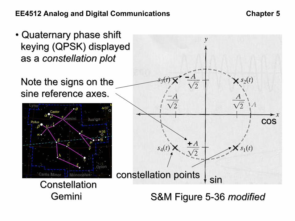
•• Quaternary phase shift keying (MQuaternary phase shift keying (M--ary, M = 2ary, M = 2nn = 4 or QPSK) = 4 or QPSK) source codes source codes dibits dibits bbii--11bbii as a as a symbolsymbol with one possible with one possible protocolprotocol as:as:
bbii--11bbii = = 11 A sin(211 A sin(2ππ ffC C t + 45t + 45°°))bbii--11bbii = = 10 A sin(210 A sin(2ππ ffC C t + 135t + 135°°))bbii--11bbii = = 00 A sin(200 A sin(2ππ ffC C t + 225t + 225°°))bbii--11bbii = = 01 A sin(201 A sin(2ππ ffCC t + 315t + 315°°))
The The Gray codeGray code is used asis used asfor Mfor M--ary PAM to improve ary PAM to improve the BER performance bythe BER performance bymitigating adjacent symbolmitigating adjacent symbolerror. The symbols are besterror. The symbols are bestdisplayed as a constellation plotdisplayed as a constellation plot S&M Figure 5S&M Figure 5--36 36 modifiedmodified
−
+
EE4512 Analog and Digital Communications Chapter 5
•• Quaternary phase shiftQuaternary phase shiftkeying (QPSK) displayedkeying (QPSK) displayedas a as a constellation plotconstellation plot
Note the signs on theNote the signs on thesine reference axes.sine reference axes.
S&M Figure 5S&M Figure 5--36 36 modifiedmodified
−
+
coscos
sinsinconstellation pointsconstellation pointsConstellationConstellation
GeminiGemini

EE4512 Analog and Digital Communications Chapter 5
Chapter 3Chapter 3
Bandpass Modulation and Bandpass Modulation and DemodulationDemodulation•• Multilevel (MMultilevel (M--ary) Phase Shiftary) Phase ShiftKeyingKeying
•• Pages 117Pages 117--123123
EE4512 Analog and Digital Communications Chapter 5
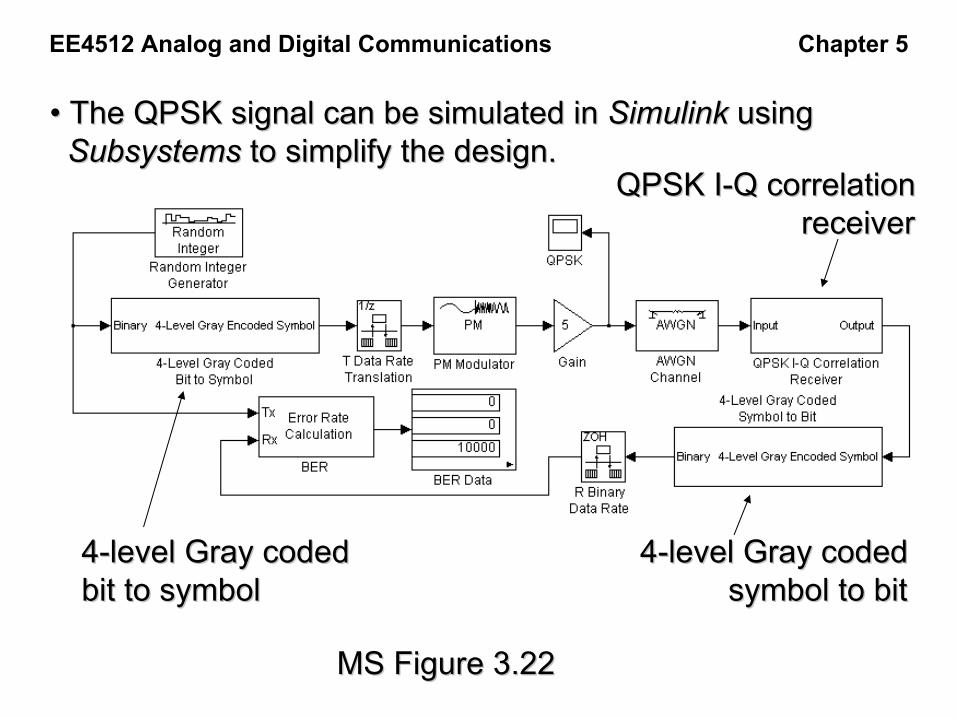
•• The QPSK signal can be simulated in The QPSK signal can be simulated in SimulinkSimulink using using SubsystemsSubsystems to simplify the design.to simplify the design.
44--level Gray coded level Gray coded symbol to bitsymbol to bit
44--level Gray coded level Gray coded bit to symbolbit to symbol
MS Figure 3.22MS Figure 3.22
QPSK IQPSK I--Q correlation Q correlation receiverreceiver

EE4512 Analog and Digital Communications Chapter 5
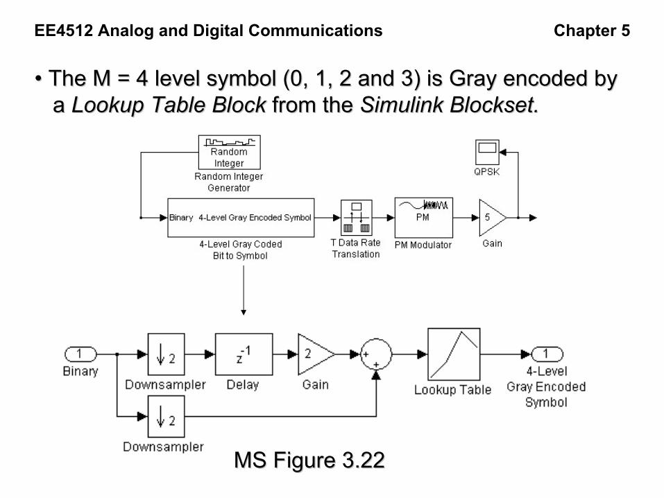
•• The random binary data source is converted to an M = 4 The random binary data source is converted to an M = 4 level Gray encoded symbol by a level Gray encoded symbol by a Simulink SubsystemSimulink Subsystem..
MS Figure 3.22MS Figure 3.22
EE4512 Analog and Digital Communications Chapter 5
•• The M = 4 level symbol (0, 1, 2 and 3) is Gray encoded by The M = 4 level symbol (0, 1, 2 and 3) is Gray encoded by a a Lookup Table Block Lookup Table Block from the from the Simulink Simulink BlocksetBlockset..
MS Figure 3.22MS Figure 3.22

EE4512 Analog and Digital Communications Chapter 5
•• The M = 4 level symbolThe M = 4 level symbol(0, 1, 2 and 3) is Gray(0, 1, 2 and 3) is Grayencoded by a encoded by a LookupLookupTable Block Table Block from thefrom theSimulink Simulink BlocksetBlockset..

EE4512 Analog and Digital Communications Chapter 5
•• The M = 4 level symbol (0, 1, 2, and 3) is Gray encoded by The M = 4 level symbol (0, 1, 2, and 3) is Gray encoded by a a Lookup Table Block Lookup Table Block by by mappingmapping [0, 1, 2, 3] to [0, 1, 3, 2][0, 1, 2, 3] to [0, 1, 3, 2]
Gray coding 00 → 0001 → 0110 → 1111 → 10

EE4512 Analog and Digital Communications Chapter 5
•• The M = 4 level symbolThe M = 4 level symbolis inputted to the Phaseis inputted to the PhaseModulator block with aModulator block with acarrier frequency carrier frequency ffCC ==20 kHz, initial phase20 kHz, initial phaseφφoo = = ππ/4/4 and a phaseand a phasedeviation factordeviation factorkkpp = = ππ/2 / V/2 / V

EE4512 Analog and Digital Communications Chapter 5
•• The M = 4 level symbol (0, 1, 2, 3) and the carrier The M = 4 level symbol (0, 1, 2, 3) and the carrier frequency frequency ffCC = 20 kHz, initial phase = 20 kHz, initial phase φφoo = = ππ/4/4 and a phase and a phase deviation factor deviation factor kkpp = = ππ/2 / V produces the phase shifts:/2 / V produces the phase shifts:
ddii = 0 = 0 φφ = = ππ/4 + 0(/4 + 0(ππ/2) = /2) = ππ/4/4ddii = 1 = 1 φφ = = ππ/4 + 1(/4 + 1(ππ/2) = 3/2) = 3ππ/4/4ddii = 2 = 2 φφ = = ππ/4 + 2(/4 + 2(ππ/2) = 5/2) = 5ππ/4/4ddii = 3 = 3 φφ = = ππ/4 + 3(/4 + 3(ππ/2) = 7/2) = 7ππ/4/4 MS Figure 3.22MS Figure 3.22

EE4512 Analog and Digital Communications Chapter 5
•• The modulation The modulation phase shifts are the phase angle phase shifts are the phase angle φφ of the of the sinusoidal carrier A sin (2sinusoidal carrier A sin (2ππ ffC C t + t + φφ) in QPSK.) in QPSK.
ddii = 0 = 0 φφ = = ππ/4 + 0(/4 + 0(ππ/2) = /2) = ππ/4/4 45°°ddii = 1 = 1 φφ = = ππ/4 + 1(/4 + 1(ππ/2) = 3/2) = 3ππ/4 135/4 135°°ddii = 2 = 2 φφ = = ππ/4 + 2(/4 + 2(ππ/2) = 5/2) = 5ππ/4 225/4 225°°ddii = 3 = 3 φφ = = ππ/4 + 3(/4 + 3(ππ/2) = 7/2) = 7ππ/4 315/4 315°°
MS Figure 3.22MS Figure 3.22

EE4512 Analog and Digital Communications Chapter 5
•• The QPSK signal can be resolved into InThe QPSK signal can be resolved into In--phase (I, cosine) phase (I, cosine) and Quadrature (Q, sine)and Quadrature (Q, sine)components. For example,components. For example,if if φφ = = ππ/4 = 45/4 = 45°°::
ss11(t) = A sin(2(t) = A sin(2ππ ffC C t + 45t + 45°°) =) =
A /A /√√2 [ I sin (22 [ I sin (2ππ ffCC t)t)+ Q cos (2+ Q cos (2ππ ffCC t) ] =t) ] =
A /A /√√2 [ sin (22 [ sin (2ππ ffC C t)t)+ cos (2+ cos (2ππ ffC C t) ]t) ]
S&M Figure 5S&M Figure 5--36 36 modifiedmodified
sin Insin In--phasephase
cos
Quadrature
constellationconstellationPlotPlot
+
−

EE4512 Analog and Digital Communications Chapter 5
•• The QPSK signal is derived from Gray coded dibits with The QPSK signal is derived from Gray coded dibits with 00 00 →→ 00 (0), 01 00 (0), 01 →→ 01 (1), 10 01 (1), 10 →→ 11 (3) and 11 11 (3) and 11 →→ 10 (2)10 (2). .
rrbb = 1 kb/sec= 1 kb/sec
QPSK signalQPSK signal
3 2 0 2 0 1 1 3 2 0 2 0 1 1 22
±± 5 V, 5 V, ffCC = 2 kHz, = 2 kHz, rrSS = 500 Hz= 500 Hz
10 11 10 11 1111 01 01 0101 1111
00 00 0000
TTS S = = 2 msec2 msec
DelayDelayM = 4M = 4

EE4512 Analog and Digital Communications Chapter 5
•• The QPSK signal can be decomposed into I and Q BPSK The QPSK signal can be decomposed into I and Q BPSK signals which are signals which are orthogonalorthogonal to each other.to each other.
QPSK signal, QPSK signal, ffCC = 2 kHz, = 2 kHz, rrSS = 500 b/sec= 500 b/sec
Binary PSK signal, sine carrierBinary PSK signal, sine carrier (I)(I)
Binary PSK signal, cosine carrier (Q)Binary PSK signal, cosine carrier (Q)
±± 5 V5 V
±± 5 / 5 / √√2 = 3.536 V2 = 3.536 V
±± 5 / 5 / √√2 = 3.536 V2 = 3.536 V
TTS S = 2 msec= 2 msec

EE4512 Analog and Digital Communications Chapter 5
•• The The orthogonalityorthogonality of the I and Q components of the QPSK of the I and Q components of the QPSK signal can be exploited by the signal can be exploited by the universal coherent receiveruniversal coherent receiver. . The orthogonal I and Q components actually occupy the The orthogonal I and Q components actually occupy the same spectrumsame spectrum without interference. The coherent without interference. The coherent reference signals are:reference signals are:
Quadrature InQuadrature In--phasephasess11(t) = cos (2(t) = cos (2ππ ffCC t + t + θθ) s) s22(t) = sin (2(t) = sin (2ππ ffCC t + t + θθ))
S&M Figure 5S&M Figure 5--4040

EE4512 Analog and Digital Communications Chapter 5
•• The orthogonality of the QPSK signals can be shown by The orthogonality of the QPSK signals can be shown by observing the output of the quadrature correlator to the I observing the output of the quadrature correlator to the I and Q signal.and Q signal.
∫
∫
∫
i
1 I Q (i-1)
i
1 I(i-1)
i2
Q(i-1)
1 Q
γ Az (n ) = d sin(2π t) + d cos(2π t) cos (2π t) dt2
γ Az (n ) = d sin(2π t) cos (2π t) dt + 2
γ A d cos (2π t) dt2
γ A z (n ) = d2 2
S
S
S
S
S
S
T
S C C CT
T
S C CT
T
CT
SS
T f f f
T f f
f
TTzz11(nT(nTSS))
S&M Eq. 5.109S&M Eq. 5.109
0
EE4512 Analog and Digital Communications Chapter 5
•• The probability of bit error The probability of bit error PPbb and the energy per bit and the energy per bit EEbb for a for a QPSK signal is the same as that as for a BPSK signal but QPSK signal is the same as that as for a BPSK signal but with a I and Q carrier amplitude of A / with a I and Q carrier amplitude of A / √√22 ..
zz11(nT(nTSS))
S&M Eq. 5.117S&M Eq. 5.117
2 2
2 2
2 γ A = Q = Q
2 γ A = Q = Q2
b, PSK bb, BPSK
o o
b, QPSK Sb, QPSK
o o
E TPN N
E TPN N
2 2
2 2
γ A= 2
γ A= 4
bb, BPSK
Sb, QPSK
TE
TEnote TS
note TS

EE4512 Analog and Digital Communications Chapter 5
•• Since Since TTSS = 2 = 2 TTb b BPSK and QPSK have the same BPSK and QPSK have the same PPbb but but QPSK can have QPSK can have twicetwice the data rate the data rate rrbb = 2 = 2 rrS S within the within the samesamebandwidth because of the orthogonal I and Q components.bandwidth because of the orthogonal I and Q components.
zz11(nT(nTSS))
2 2 2 γ A = = Q = Qb bb, BPSK b, QPSK
o o
E TP PN N
2 2γ A= =2
bb, BPSK b, QPSK
TE E

EE4512 Analog and Digital Communications Chapter 5
•• QPSK coherent digital communication system with BER QPSK coherent digital communication system with BER analysis:analysis:
MS Figure 3.22MS Figure 3.22
44--Level Gray codedLevel Gray codedbit to symbolbit to symbol
44--Level Gray codedLevel Gray codedsymbol to bitsymbol to bit
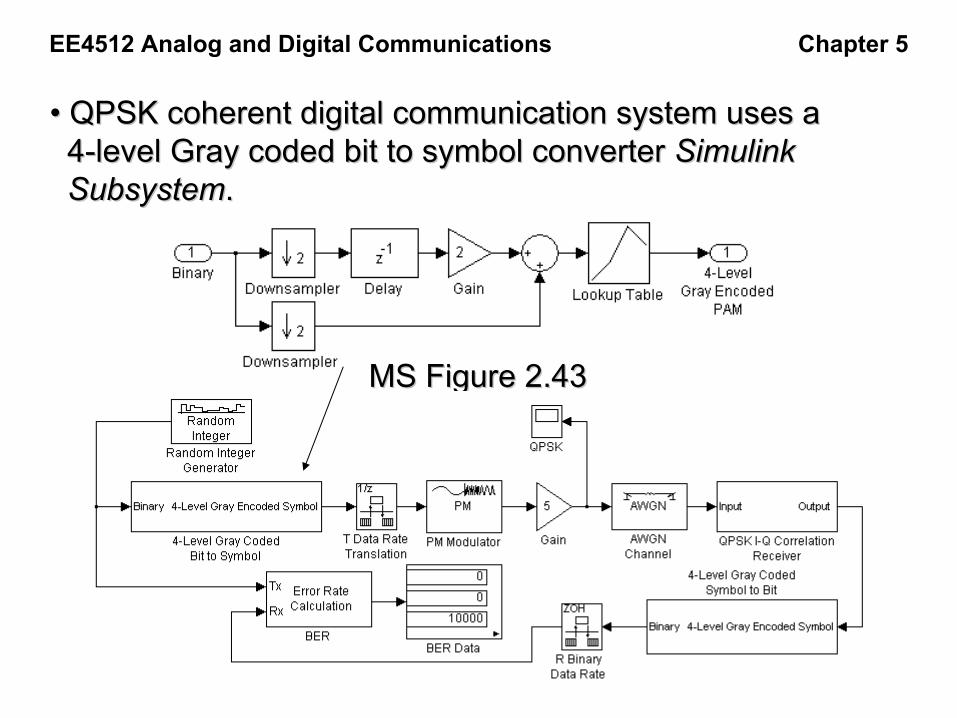
EE4512 Analog and Digital Communications Chapter 5
•• QPSK coherent digital communication system uses aQPSK coherent digital communication system uses a44--level Gray coded bit to symbol converter level Gray coded bit to symbol converter SimulinkSimulinkSubsystemSubsystem. .
MS Figure 2.43MS Figure 2.43
EE4512 Analog and Digital Communications Chapter 5
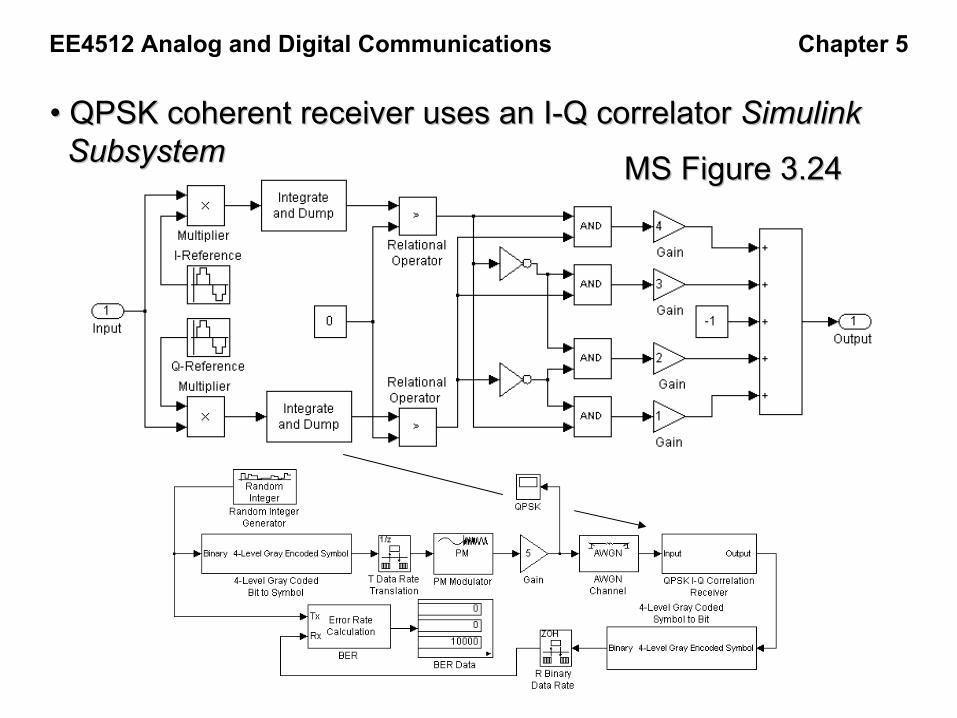
•• QPSK coherent receiver uses an IQPSK coherent receiver uses an I--Q correlator Q correlator Simulink Simulink SubsystemSubsystem MS Figure 3.24MS Figure 3.24

EE4512 Analog and Digital Communications Chapter 5
•• The IThe I--Q correlation receiver is the Q correlation receiver is the universal universal structure with structure with an integration time equal to the an integration time equal to the symbol time Tsymbol time TSS..
MS Figure 3.24MS Figure 3.24
correlation receivercorrelation receiver

EE4512 Analog and Digital Communications Chapter 5
•• The output of the IThe output of the I--Q correlation receiver is a Q correlation receiver is a dibitdibit and and converted to an M = 2converted to an M = 2n n = 4 level symbols (0, 1, 2, and 3).= 4 level symbols (0, 1, 2, and 3).
dibits Mdibits M--ary scaling ary scaling MS Figure 3.24MS Figure 3.24
correlation receivercorrelation receiver

EE4512 Analog and Digital Communications Chapter 5
•• The BER and PThe BER and Pbb comparison for 4comparison for 4--PSK (QPSK): PSK (QPSK):
Table 3.11Table 3.11 Observed BER and Theoretical UpperObserved BER and Theoretical Upper--Bound Bound of of PPbb as a Function of as a Function of EEb b / N/ Noo in a Gray coded 4in a Gray coded 4--PSK PSK (QPSK) Digital Communication System with Optimum (QPSK) Digital Communication System with Optimum ReceiverReceiver
EEdd//NNoo dBdB BERBER PPbb∞∞ 00 001212 00 ≈≈1010--88
1010 00 ≈≈1010--66
88 2 2 ×× 1010--44 ≈≈1010--44
66 2.3 2.3 ×× 1010--33 2.4 2.4 ×× 1010--33
44 1.20 1.20 ×× 1010--22 1.25 1.25 ×× 1010--22
22 3.62 3.62 ×× 1010--22 3.75 3.75 ×× 1010--22
00 7.65 7.65 ×× 1010--22 7.85 7.85 ×× 1010--22

EE4512 Analog and Digital Communications Chapter 5
•• The The singlesingle--sidedsided power spectral density PSD of the QPSK power spectral density PSD of the QPSK signal uses signal uses rrss = = rrb b /2 and is:/2 and is:
GGQPSKQPSK(f(f) = 1/2 ) = 1/2 GGPAMPAM(f(f -- ffCC))GGPAMPAM(f(f) = A) = A2 2 / / rrss sincsinc22 ((ππ f / f / rrss))
No carrierNo carrier
SincSinc22
rrss = 500 s/sec, = 500 s/sec, rrbb = 1 kb/sec= 1 kb/sec
MS Figure 3.25MS Figure 3.25

EE4512 Analog and Digital Communications Chapter 5
•• The The singlesingle--sidedsided power spectral density PSD of BPSK has power spectral density PSD of BPSK has double double the bandwidth than that for QPSK for the same bit the bandwidth than that for QPSK for the same bit rate rate rrbb = 1/= 1/TTbb,,
No carrierNo carrierSincSinc22
rrbb = 1 kHz= 1 kHz
MS Figure 3.14MS Figure 3.14

EE4512 Analog and Digital Communications Chapter 5
•• The The bandwidthbandwidth of a QPSK signal as a percentage of total of a QPSK signal as a percentage of total power is power is half half that for the same bit rate rthat for the same bit rate rb b = 1/T= 1/Tbb BPSK BPSK signal since signal since rrss = = rrb b /2 or /2 or TTss = 2= 2TTbb (MS Table 3.9). (MS Table 3.9).
Bandwidth (Hz) Percentage of Total PowerBandwidth (Hz) Percentage of Total Power
2/2/TTss 1/1/TTbb 90%90%3/3/TTss 1.5/1.5/TTbb 93%93%4/4/TTss 2/2/TTbb 95%95%6/6/TTss 3/3/TTbb 96.5%96.5%8/8/TTss 4/4/TTbb 97.5%97.5%10/10/TTss 5/5/TTbb 98%98%

EE4512 Analog and Digital Communications Chapter 5
Chapter 5Chapter 5
Digital Bandpass ModulationDigital Bandpass Modulationand Demodulationand DemodulationTechniquesTechniques•• MM--ary Bandpass Techniques:ary Bandpass Techniques:88--Phase Shift KeyingPhase Shift Keying
•• Pages 286Pages 286--292292

EE4512 Analog and Digital Communications Chapter 5
•• MM--ary phase shift keying (M = 8 or 8PSK) source codes ary phase shift keying (M = 8 or 8PSK) source codes tribitstribits bbii--22bbii--11bbii as a as a symbolsymbol with one possible with one possible protocolprotocol as:as:
bbii--22bbii--11bbii = = 000 A sin(2000 A sin(2ππ ffC C t + 0t + 0°°))bbii--22bbii--11bbii = = 001 A sin(2001 A sin(2ππ ffC C t + 45t + 45°°))bbii--22bbii--11bbii = = 011 A sin(2011 A sin(2ππ ffC C t + 90t + 90°°))bbii--22bbii--11bbii = = 010 A sin(2010 A sin(2ππ ffC C t + 135t + 135°°))bbii--22bbii--11bbii = = 110 A sin(2110 A sin(2ππ ffC C t + 180t + 180°°))bbii--22bbii--11bbii = = 111 A sin(2111 A sin(2ππ ffC C t + 225t + 225°°))bbii--22bbii--11bbii = = 101 A sin(2101 A sin(2ππ ffC C t + 270t + 270°°))bbii--22bbii--11bbii = = 100 A sin(2100 A sin(2ππ ffC C t + 315t + 315°°))
θθI, Q = 0, I, Q = 0, ±± 1/1/√√2, 2, ±± 1 1 s(ts(t) =) = A [ I sin (2A [ I sin (2ππ ffC C t) + t) +
Q cos (2Q cos (2ππ ffC C t) ]t) ] S&M Figure 5S&M Figure 5--4343
sin Insin In--phasephase
Quadrature
cos
Constellation PlotConstellation Plot

EE4512 Analog and Digital Communications Chapter 5
•• The correlation receiverThe correlation receiverfor 8for 8--PSK uses fourPSK uses fourreference signals:reference signals:
ssrefref nn(t(t) = ) = sin (2sin (2ππ ffC C t + t +
n 45n 45°° + 22.5+ 22.5°°))φφ
n = 0, 1, 2, 3n = 0, 1, 2, 3φφ = 22.5= 22.5°°, 67.5, 67.5°°,,
112.5112.5°°, 157.5, 157.5°°
S&M Eq. 5.124S&M Eq. 5.124

EE4512 Analog and Digital Communications Chapter 5
•• The output from any one of the four correlators is:The output from any one of the four correlators is:
− −
−
∫
∫ ∫
i
1(i-1)
i i
1(i-1) (i-1)
1
z (n ) = γ A sin (2π t + θ) sin (2π t + φ)dt
γ Az (n ) = cos (θ φ) dt cos (4π t + θ + φ) dt2
γ A z (n ) = cos (θ φ)2
S
S
S S
S S
T
S C CT
T T
S CT T
SS
T f f
T f
TT
zz11((nnTTSS))
S&M Eq. 5.125S&M Eq. 5.125
0

EE4512 Analog and Digital Communications Chapter 5
•• The correlator output is > 0 if | The correlator output is > 0 if | θθ –– φφ | < 90| < 90°° and < 0 if notand < 0 if notbecause of the cos (because of the cos (θθ –– φφ) term. For example, if s) term. For example, if s66(t) is (t) is received, the received, the ABCDABCD correlator sign output is: correlator sign output is: –– –– –– +. The +. The patterns of signs are unique and can be decoded to bpatterns of signs are unique and can be decoded to bii--22bbii--11bbii
(S&M Tab(S&M Tables 5les 5--7 and 57 and 5--8)8)
zz11((nnTTSS))A: A: ssrefref 11(t)(t)
B: B: ssrefref 22(t)(t)
C: C: ssrefref 33(t)(t)
D: D: ssrefref 44(t)(t)

EE4512 Analog and Digital Communications Chapter 5
•• The probability of The probability of symbol errorsymbol error PPSS for coherently for coherently demodulated Mdemodulated M--ary PSK is:ary PSK is:
≈ ≥
≈ ≥
22
22
A π2Q sin M 4M
π2Q 2 log M sin M 4M
SS coherent M-ary PSK
o
bS coherent M-ary PSK
o
TPN
EPN
S&M Eq. 5.126S&M Eq. 5.126
S&M Figure 5S&M Figure 5--4646
EEb b / / NNo o dBdB
PPss

EE4512 Analog and Digital Communications Chapter 5
•• The probability of The probability of symbol errorsymbol error PPSS for coherently for coherently demodulated Mdemodulated M--ary PSK is:ary PSK is:
S&M Figure 5S&M Figure 5--4646
EEbb//NNo o dBdB
PPss

EE4512 Analog and Digital Communications Chapter 5
•• The probability of symbol error The probability of symbol error PPSS must be related to must be related to probability of bit error probability of bit error PPbb for consistency. If for consistency. If Gray codingGray coding is is used, assume that errors will only be due to used, assume that errors will only be due to adjacent adjacent symbolssymbols. Thus each symbol error produces only one bit in. Thus each symbol error produces only one bit inerror and logerror and log22 (M (M –– 1) correct bits or:1) correct bits or:
However for MHowever for M--ary PSK with M > 4 the assumption of errors ary PSK with M > 4 the assumption of errors being due to only adjacent symbols is invalid. For the being due to only adjacent symbols is invalid. For the worst case there are M worst case there are M –– 1 incorrect symbols and in M / 2 of 1 incorrect symbols and in M / 2 of these a bit will different from the correct bit so that:these a bit will different from the correct bit so that:
2
1= log Mb errors due to adjacent symbols SP P S&M Eq. 5.127S&M Eq. 5.127
≤ ≤−2
1 M log M 2 (M 1)S b SP P P S&M Eq. 5.129S&M Eq. 5.129

EE4512 Analog and Digital Communications Chapter 5
Chapter 5Chapter 5
Digital Bandpass ModulationDigital Bandpass Modulationand Demodulationand DemodulationTechniquesTechniques•• MM--ary Bandpass Techniques:ary Bandpass Techniques:Quaternary Frequency Shift KeyingQuaternary Frequency Shift Keying
•• Pages 292Pages 292--298298

EE4512 Analog and Digital Communications Chapter 5
•• The analytical signal for quaternary (MThe analytical signal for quaternary (M--ary, M = 2ary, M = 2nn = 4) = 4) frequency shift keying (QFSK or 4frequency shift keying (QFSK or 4--FSK) is:FSK) is:
ss44--FSKFSK(t) =(t) = A sin (2A sin (2ππ ((ffCC + 3+ 3∆∆ff) t + ) t + θθ) if b) if bii--11bbii = 11= 11ss44--FSKFSK(t) = A sin (2(t) = A sin (2ππ ((ffCC + + ∆∆ff) t + ) t + θθ) if b) if bii--11bbii = 10= 10ss44--FSKFSK(t) = A sin (2(t) = A sin (2ππ ((ffCC –– ∆∆ff) t + ) t + θθ) if b) if bii--11bbii = 00 = 00 ss44--FSKFSK(t) = A sin (2(t) = A sin (2ππ ((ffCC –– 33∆∆ff) t + ) t + θθ) if b) if bii--11bbi i = 01= 01
ffCC + 3+ 3∆∆ff ffCC –– 33∆∆ff ffCC + + ∆∆ffffCC –– ∆∆ff ffCC + 3+ 3∆∆ff11 00 01 10 1111 00 01 10 11
MS Figure 3.19MS Figure 3.19

EE4512 Analog and Digital Communications Chapter 5
•• Chose Chose ffCC and and ∆∆ff so that if there are a whole number of half so that if there are a whole number of half cycles of a sinusoid within a symbol time cycles of a sinusoid within a symbol time TTSS for M = 4 forfor M = 4 fororthogonality of the signals so that a correlation receiver orthogonality of the signals so that a correlation receiver can be utilized.can be utilized.
ss44--FSKFSK(t) =(t) = A sin (2A sin (2ππ ((ffCC + 3+ 3∆∆ff) t + ) t + θθ) if b) if bii--11bbii = 11= 11ss44--FSKFSK(t) = A sin (2(t) = A sin (2ππ ((ffCC + + ∆∆ff) t + ) t + θθ) if b) if bii--11bbii = 10= 10ss44--FSKFSK(t) = A sin (2(t) = A sin (2ππ ((ffCC –– ∆∆ff) t + ) t + θθ) if b) if bii--11bbii = 00 = 00 ss44--FSKFSK(t) = A sin (2(t) = A sin (2ππ ((ffCC –– 33∆∆ff) t + ) t + θθ) if b) if bii--11bbi i = 01= 01
MS Figure 3.19MS Figure 3.19

EE4512 Analog and Digital Communications Chapter 5
•• The correlation receiverThe correlation receiverfor 4for 4--FSK uses fourFSK uses fourreference signals:reference signals:
ssrefref nn(t(t) = ) = sin (2sin (2ππ ((ffCC + n + n ∆∆ff)) t)t)
n = n = ±±1, 1, ±±33
S&M Figure 5S&M Figure 5--4949

EE4512 Analog and Digital Communications Chapter 5
•• The probability of The probability of symbol errorsymbol error PPSS for coherently for coherently demodulated Mdemodulated M--ary FSK is:ary FSK is:
≤ − ≥
=
− ≥
2
S coherent M-ary FSK
S coherent M-ary FSK
2
AP (M 1) Q M 42
P
(M 1) Q log M M 4
s
o
b
o
TN
EN
S&M Eq. 5.132S&M Eq. 5.132
S&M Figure 5S&M Figure 5--5151
EEbb/N/No o dBdB
PPss

EE4512 Analog and Digital Communications Chapter 5
•• The probability of The probability of symbol errorsymbol error PPSS for coherently for coherently demodulated Mdemodulated M--ary FSK is:ary FSK is:
S&M Figure 5S&M Figure 5--5151
EEbb//NNoodBdB
PPss

EE4512 Analog and Digital Communications Chapter 5
Chapter 3Chapter 3
Bandpass Modulation and Bandpass Modulation and DemodulationDemodulation•• Multilevel (MMultilevel (M--ary) Frequencyary) FrequencyShift KeyingShift Keying
•• Pages 110Pages 110--116116

EE4512 Analog and Digital Communications Chapter 5
•• 44--FSK coherent digital communication system with BER FSK coherent digital communication system with BER analysis:analysis:
MS Figure 3.18MS Figure 3.18

EE4512 Analog and Digital Communications Chapter 5
•• The dibits are converted to a symbol and scaled. The data The dibits are converted to a symbol and scaled. The data is is not not Gray encoded. For MGray encoded. For M--ary FSK symbol errors are ary FSK symbol errors are equally likely among the M equally likely among the M –– 1 correlators and there is 1 correlators and there is no no advantageadvantage to Gray encoding.to Gray encoding.
MS Figure 3.18MS Figure 3.18

EE4512 Analog and Digital Communications Chapter 5
•• 44--FSK coherent digital communication system with BER FSK coherent digital communication system with BER analysis:analysis:
44--FSK correlation receiverFSK correlation receiver
MS Figure 3.18MS Figure 3.18

EE4512 Analog and Digital Communications Chapter 5
•• 44--FSK coherent digital communication system with BER FSK coherent digital communication system with BER analysis:analysis: 44--FSK correlation receiverFSK correlation receiver
MS Figure 3.20MS Figure 3.20

EE4512 Analog and Digital Communications Chapter 5
•• The 4The 4--FSK correlationFSK correlationreceiver has fourreceiver has fourcorrelators with ancorrelators with anintegration time equalintegration time equalto the to the symbol time Tsymbol time TSS..

EE4512 Analog and Digital Communications Chapter 5
•• The symbols are converted to dibits. The original data is The symbols are converted to dibits. The original data is not not Gray encoded and is therefore Gray encoded and is therefore notnot Gray decodedGray decoded..
MS Figure 3.18MS Figure 3.18

EE4512 Analog and Digital Communications Chapter 5
•• The BER and PThe BER and Pbb comparison for 4comparison for 4--FSK: FSK:
Table 3.10Table 3.10 Observed BER and Theoretical Upper Bound Observed BER and Theoretical Upper Bound of of PPbb as a Function of as a Function of EEb b / N/ Noo in 4in 4--level FSK Digital level FSK Digital Communication System with Optimum ReceiverCommunication System with Optimum Receiver
EEdd//NNoo dBdB BERBER PPbb∞∞ 00 001212 00 ≈≈1010--88
1010 00 ≈≈1010--66
88 1 1 ×× 1010--44 ≈≈1010--44
66 5.1 5.1 ×× 1010--33 4.8 4.8 ×× 1010--33
44 2.26 2.26 ×× 1010--22 2.52 2.52 ×× 1010--22
22 5.97 5.97 ×× 1010--22 7.54 7.54 ×× 1010--22
00 1.209 1.209 ×× 1010--11 1.586 1.586 ×× 1010--11

EE4512 Analog and Digital Communications Chapter 5
•• The The singlesingle--sidedsided power spectral density PSD with a power spectral density PSD with a minimum carrier frequency deviation (MFSK) for Mminimum carrier frequency deviation (MFSK) for M--ary ary FSK is FSK is ∆∆ff = 1/2= 1/2TTS S = = rrSS/2. /2. For MFSK the carriers should be For MFSK the carriers should be spaced at multiples of 2spaced at multiples of 2∆∆f = 1/f = 1/TTSS == rrSS (S&M Eq. 5.131 is(S&M Eq. 5.131 isincorrectincorrect). Here ). Here ∆∆ff = 2 = 2 rrSS = 1 kHz
SincSinc22
rrss = 500 s/sec, = 500 s/sec, rrbb = 1 kb/sec= 1 kb/sec
MS Figure 3.21MS Figure 3.21
∆∆f f = 1 kHz= 1 kHzM = 4M = 4

EE4512 Analog and Digital Communications Chapter 5
•• The The bandwidthbandwidth of a Mof a M--ary FSK signal as a percentage of ary FSK signal as a percentage of total power (MS Table 3.9). total power (MS Table 3.9).
Bandwidth (Hz) Percentage of Total PowerBandwidth (Hz) Percentage of Total Power
2( M 2( M –– 1) 1) ∆∆f f + + 4/4/TTss 95%95%2 (M 2 (M –– 1) 1) ∆∆f f + + 6/6/TTss 96.5%96.5%2 (M 2 (M –– 1) 1) ∆∆f f + + 8/8/TTss 97.5%97.5%2 (M 2 (M –– 1) 1) ∆∆ff + + 10/10/TTss 98%98%
For MFSK: For MFSK: ∆∆ff = 1/2= 1/2TTSS = = rrSS/2/2M = 2M = 2n n and and rrSS = = rrbb/n/n

EE4512 Analog and Digital Communications Chapter 5
Chapter 5Chapter 5
Digital Bandpass ModulationDigital Bandpass Modulationand Demodulationand DemodulationTechniquesTechniques•• MM--ary Bandpass Techniques:ary Bandpass Techniques:Quadrature Amplitude ModulationQuadrature Amplitude Modulation
•• Pages 298Pages 298--301301

EE4512 Analog and Digital Communications Chapter 5
•• The analytical signal for quadrature amplitude modulation The analytical signal for quadrature amplitude modulation (QAM) has I(QAM) has I--Q components:Q components:
ssQAMQAM(t(t) = I sin (2) = I sin (2ππ ffCCtt) + Q cos (2) + Q cos (2ππ ffCCtt))
A QAM signal has A QAM signal has both both amplitudeamplitude and and phasephasecomponents which can becomponents which can beshown in the shown in the constellationconstellationplotplot..
S&M Figure 5S&M Figure 5--5353I
Q
16-ary QAM

EE4512 Analog and Digital Communications Chapter 5
•• An MAn M--ary PSK signal also has Iary PSK signal also has I--Q components but the Q components but the amplitude is amplitude is constantconstant and only the phase and only the phase variesvaries::
ssQAMQAM(t(t) = I sin (2) = I sin (2ππ ffCCtt) + Q cos (2) + Q cos (2ππ ffCCtt))
S&M Figure 5S&M Figure 5--5454
II
II
1616--ary ary PSKPSK
1616--ary ary QAMQAM

EE4512 Analog and Digital Communications Chapter 5
•• The The orthogonalityorthogonality of the I and Q components of the QAM of the I and Q components of the QAM signal can be exploited by the signal can be exploited by the universal coherent receiveruniversal coherent receiver. . The orthogonal I and Q components actually occupy the The orthogonal I and Q components actually occupy the same spectrumsame spectrum without interference. The coherent without interference. The coherent reference signals are:reference signals are:
Quadrature InQuadrature In--phasephasess11(t) = cos (2(t) = cos (2ππ ffCCtt) s) s22(t) = sin (2(t) = sin (2ππ ffCCtt))
S&M Figure 5S&M Figure 5--5555

EE4512 Analog and Digital Communications Chapter 5
•• An An upperupper--boundbound for the probability of for the probability of symbol errorsymbol error PPSS for for coherently demodulated Mcoherently demodulated M--ary QAM is:ary QAM is:
4
≤ − S coherent M-ary QAM
3 P Q(M 1)
s
o
EN S&M Eq. 5.135S&M Eq. 5.135
QAM BER curveQAM BER curve M = 256M = 256
M = 4M = 4

EE4512 Analog and Digital Communications Chapter 5
•• An MAn M--ary QAM constellation plot shows the ary QAM constellation plot shows the stabilitystability of the of the signaling and the signaling and the transitiontransition from one signal to another:from one signal to another:
256256--ary QAMary QAM1616--ary QAMary QAM

EE4512 Analog and Digital Communications Chapter 5
Chapter 3Chapter 3
Bandpass Modulation and Bandpass Modulation and DemodulationDemodulation•• Quadrature AmplitudeQuadrature AmplitudeModulationModulation
•• Pages 123Pages 123--130130

EE4512 Analog and Digital Communications Chapter 5
•• QAM coherent digital communication system with BER QAM coherent digital communication system with BER analysis:analysis:
MS Figure 3.26MS Figure 3.26
1616--QAM correlation QAM correlation receiverreceiver
4 bit to I,Q symbol 4 bit to I,Q symbol
QAMQAM
1616--level symbol to bitlevel symbol to bit

EE4512 Analog and Digital Communications Chapter 5
•• QAM coherent digital communication system with BER QAM coherent digital communication system with BER analysis: 4 bit to Ianalysis: 4 bit to I--Q symbol SQ symbol Simulink imulink subsystem.subsystem.
MS Figure 3.27MS Figure 3.27

EE4512 Analog and Digital Communications Chapter 5
•• QAM coherent digital communication system with BER QAM coherent digital communication system with BER analysis: Table 3.12 I and Q output amplitudesanalysis: Table 3.12 I and Q output amplitudes
Input IInput I Q Q InputInput I I QQ InputInput II QQ00 ––11 11 55 1 31 3 1010 ––33 ––1111 ––33 11 66 3 13 1 1111 ––33 ––3322 ––1 1 ––33 77 3 33 3 1212 11 ––1133 ––33 33 88 ––1 1 ––11 1313 33 ––1144 11 11 99 ––1 1 ––33 1414 11 ––33
1515 33 ––22
MS Figure 3.27MS Figure 3.27
I LUT I LUT ±± 1 to 1 to ±± 33Q LUTQ LUT
symbol 0 to 15symbol 0 to 15

EE4512 Analog and Digital Communications Chapter 5
•• QAM coherent digital communication system with BER QAM coherent digital communication system with BER analysis: QAM modulator Sanalysis: QAM modulator Simulink imulink subsystem.subsystem.
MS Figure 3.27MS Figure 3.27

EE4512 Analog and Digital Communications Chapter 5
•• QAM coherent digital communication system with BER QAM coherent digital communication system with BER analysis: 16analysis: 16--QAM correlation receiver SQAM correlation receiver Simulink imulink subsystem.subsystem.
MS Figure 3.30MS Figure 3.30

EE4512 Analog and Digital Communications Chapter 5
•• QAM coherent digitalQAM coherent digitalcommunication systemcommunication systemwith BER analysis:with BER analysis:Table 3.14 I, Q Symbol LUTTable 3.14 I, Q Symbol LUT1616--level output amplitudeslevel output amplitudes
II QQ OutputOutput II QQ OutputOutput11 11 1111 33 11 1111 22 99 33 22 0011 33 1414 33 33 4411 44 1515 33 44 6622 11 1010 44 11 3322 22 88 44 22 2222 33 1212 44 33 5522 44 1313 44 44 77
EE4512 Analog and Digital Communications Chapter 5
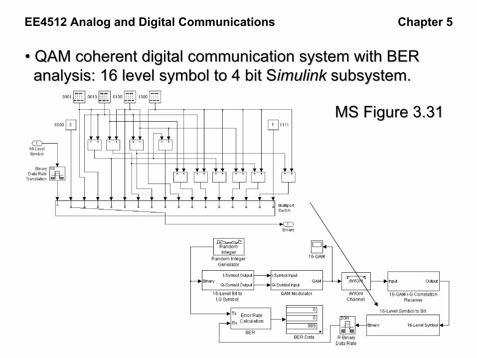
•• QAM coherent digital communication system with BER QAM coherent digital communication system with BER analysis: 16 level symbol to 4 bit Sanalysis: 16 level symbol to 4 bit Simulink imulink subsystem.subsystem.
MS Figure 3.31MS Figure 3.31

EE4512 Analog and Digital Communications Chapter 5
•• QAM coherent digital communication system with BER QAM coherent digital communication system with BER analysis: 16 level symbol to 4 bit Sanalysis: 16 level symbol to 4 bit Simulink imulink subsystem.subsystem.
MS Figure 3.31MS Figure 3.31

EE4512 Analog and Digital Communications Chapter 5
•• The The singlesingle--sidedsided power spectral density PSD of the 16power spectral density PSD of the 16--ary ary QAM has a bandwidth of 1/M that of a PSK signal with the QAM has a bandwidth of 1/M that of a PSK signal with the same data rate same data rate rrbb..
SincSinc22
rrss = 250 s/sec, = 250 s/sec, rrbb = 1 kb/sec= 1 kb/sec
MS Figure 3.32MS Figure 3.32no discrete no discrete component at fcomponent at fCC = = 20 kHz20 kHz

EE4512 Analog and Digital Communications Chapter 5
BPSK PSDBPSK PSDrrbb = 1 kb/sec= 1 kb/sec
1616--ary QAM PSDary QAM PSD
rrbb = 1 kb/sec M = 4 = 1 kb/sec M = 4 rrSS = 250 s/sec= 250 s/sec
1 kHz1 kHz
250 Hz250 Hz
EE4512 Analog and Digital Communications Chapter 5
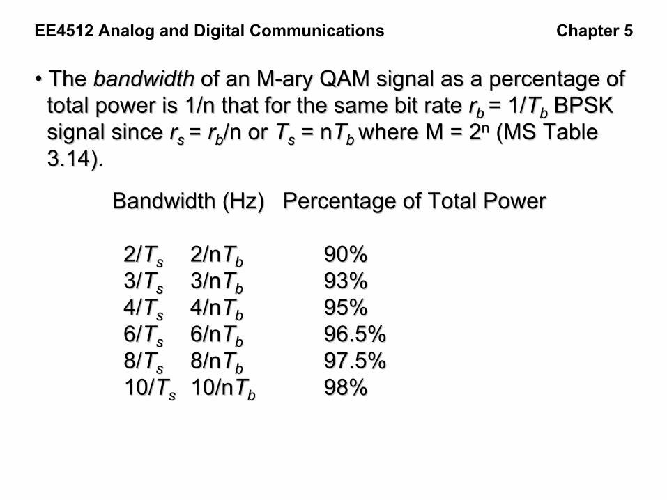
•• The The bandwidthbandwidth of an Mof an M--ary QAM signal as a percentage of ary QAM signal as a percentage of total power is 1/ntotal power is 1/n that for the same bit rate that for the same bit rate rrb b = 1/= 1/TTbb BPSK BPSK signal sincesignal since rrss = = rrbb/n or /n or TTss = n= nTTbb where M = 2where M = 2nn (MS Table (MS Table 3.14). 3.14).
Bandwidth (Hz) Percentage of Total PowerBandwidth (Hz) Percentage of Total Power
2/2/TTss 2/n2/nTTbb 90%90%3/3/TTss 3/n3/nTTbb 93%93%4/4/TTss 4/n4/nTTbb 95%95%6/6/TTss 6/n6/nTTbb 96.5%96.5%8/8/TTss 8/n8/nTTbb 97.5%97.5%10/10/TTss 10/n10/nTTbb 98%98%

EE4512 Analog and Digital Communications Chapter 5
•• 1616--QAM coherent digital communication system receivedQAM coherent digital communication system receivedII--Q components can be displayed on as a Q components can be displayed on as a signal trajectorysignal trajectoryor or constellation plotconstellation plot ..
Figure 3.42Figure 3.42
realreal--imaginary (a + b j) imaginary (a + b j) conversion to complexconversion to complexpolar (M polar (M exp(jexp(jθθ)) conversion)) conversion

EE4512 Analog and Digital Communications Chapter 5
•• The The RealReal--Imaginary toImaginary toComplexComplex conversion blockconversion blockis in the is in the Math OperationsMath Operations,,Simulink Simulink BlocksetBlockset
Figure 3.42Figure 3.42

EE4512 Analog and Digital Communications Chapter 5
•• The constellation plotThe constellation plot(scatter plot) and(scatter plot) andsignal trajectory aresignal trajectory areCommComm Sinks Sinks blocksblocksfromfrom thetheCommunicationsCommunicationsBlocksetBlockset
Figure 3.42Figure 3.42

EE4512 Analog and Digital Communications Chapter 5
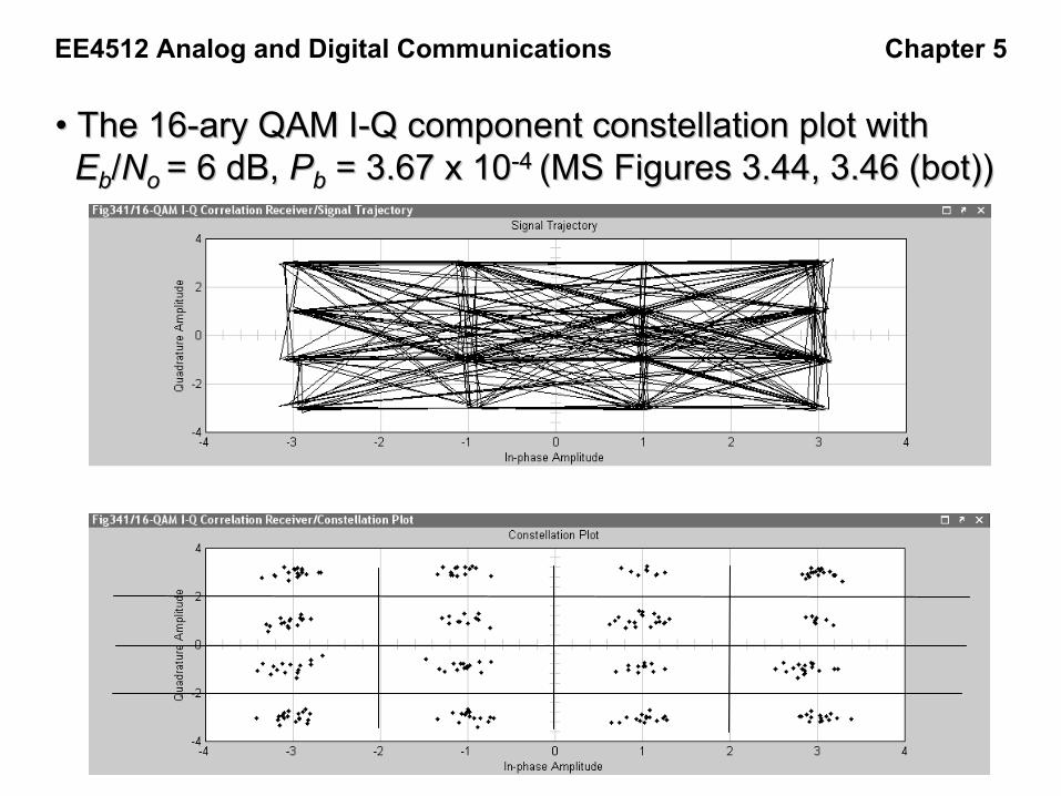
•• The 16The 16--ary QAM Iary QAM I--Q component constellation plot withQ component constellation plot withEEbb//NNo o →→ ∞∞ (MS Figures 3.43, 3.45)(MS Figures 3.43, 3.45)..
signal pointssignal points
signal transitionssignal transitions
decision boundariesdecision boundaries

EE4512 Analog and Digital Communications Chapter 5
•• The 16The 16--ary QAM Iary QAM I--Q component constellation plot withQ component constellation plot withEEbb//NNoo = = 12 dB, 12 dB, PPbb ≈≈ 1010--44 (MS Figures 3.44, 3.46 (top))(MS Figures 3.44, 3.46 (top))
EE4512 Analog and Digital Communications Chapter 5
•• The 16The 16--ary QAM Iary QAM I--Q component constellation plot withQ component constellation plot withEEbb//NNo o = 6= 6 dB, dB, PPbb = 3.67= 3.67 x 10x 10--4 4 (MS Figures 3.44, 3.46 ((MS Figures 3.44, 3.46 (botbot))))

EE4512 Analog and Digital Communications Chapter 5
End of Chapter 5End of Chapter 5
Digital Bandpass ModulationDigital Bandpass Modulationand Demodulationand DemodulationTechniquesTechniques