femtoclock ng jitter attenuator and 8v44n4614 clock
TRANSCRIPT

DATA SHEET
FemtoClock® NG Jitter Attenuator and Clock Synthesizer
8V44N4614
REVISION 1 02/25/15 1 ©2015 INTEGRATED DEVICE TECHNOLOGY, INC.
General Description
The 8V44N4614 is a FemtoClock® NG Clock Generator. The device has been designed for frequency generation in high-performance systems such wireless base-band boards, for instance to drive the reference clock inputs of processors, PHY, switch and SerDes devices. The device is very flexible in frequency programming. It allows to generate the clock frequencies of 156.25MHz, 125MHz, 100MHz and 25MHz individually at three output banks. One output bank supports configurable LVDS, LVPECL, the other two output banks support LVCMOS output levels. All outputs are synchronized on the incident rising edge, regardless of the selected output frequency. Selective single-ended LVCMOS outputs can be configured to invert the output phase, effectively forming differential LVCMOS output pairs for noise reduction. The PLL reference signal is either a 25MHz, 50MHz, 100MHz or 200MHz differential or single-ended clock.
The device is optimized to deliver excellent period and cycle-to-cycle jitter performance, combined with good phase noise performance, and high power supply noise rejection.
The device is configured through an SPI serial interface. Outputs can be configured to any of the available output frequencies. Two hardware pins are available for selecting pre-set output enable/ disable configurations. In each of these pre-set configurations, each output can be enabled/disabled individually. A separate test mode is available for an increase or decrease of the output frequencies in 19.53125ppm steps independent on the input frequency. The device is packaged in a lead-free (RoHS 6) 48-lead VFQFN package. The extended temperature range supports wireless infrastructure, telecommunication and networking end equipment requirements.
Features
• Clock generator for wireless base-band systems
• Drives reference clock inputs of processors, PHY, switch and SerDes devices
• FemtoClock® NG technology
• Three low-skew, differential LVDS, LVPECL configurable clock outputs
• Ten low-skew, LVCMOS/LVTTL clock outputs
• Input: 200MHz, 100MHz, 50MHz, 25MHz single-ended (LVCMOS) or differential reference clock (LVDS, LVPECL)
• Output clocks support 156.25MHz, 125MHz, 100MHz and 25MHz
• Individual output disable (high-impedance)
• Two sets of output enable configurations
• PLL lock detect output
• Test mode with frequency margining with 19.53125ppm steps (range ±507.8125ppm)
• LVCMOS (1.8V, JESD8-7A) compatible SPI programming interface
• Cycle-to-cycle jitter: 10ps (typical)
• RMS period jitter: 1.6ps (typical)
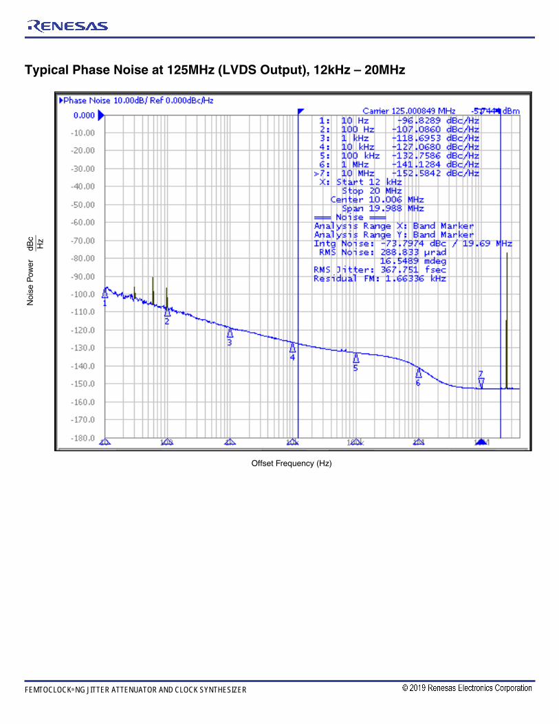
• Phase noise (12kHz - 20MHz): 0.40ps (typical)
• 3.3V core and output supply
• -40°C to +85°C ambient operating temperature
• Lead-free (RoHS 6) 48-lead VFQFN packaging

8V44N4614 DATA SHEET
FEMTOCLOCK® NG JITTER ATTENUATOR AND CLOCK SYNTHESIZER 2 REVISION 1 02/25/15
Block Diagram
CLKnCLK
LCLK
REFSELBYPASS
TEST
MISOMOSI
SPICLKnCS
OENAOENB
LOCK
QA0, nQA0
QA1, nQA1
QA2, nQA2
QA3
QA4
QB0
QB1
QB2
QB3
QC0
QC1
QC2
QC3
PulldownPulldownPulldown
÷M
FemtoClock NG PLL2500 MHz
0
1
1
0
PullupPullupPullup
SPI Slave Controller
Register File6
13
Power-up Reset
÷16÷20÷25
÷100
NA
÷16÷20÷25
÷100
NC
÷16÷20÷25
÷100
NB
÷P
÷MT
Pulldown
PullupPulldown
0
1
Pulldown
Pullup/Pulldown

8V44N4614 DATA SHEET
REVISION 1 02/25/15 3 FEMTOCLOCK® NG JITTER ATTENUATOR AND CLOCK SYNTHESIZER
Pin Assignment
Table 1: Pin Descriptions
Number Name Type Description
1, 9 VDDOA Power Supply voltage for the QA bank clock outputs (3.3V).
2, 3 QA0, nQA0 Output Differential clock output A0. LVDS or LVPECL configurable output levels.
4, 5 QA1, nQA1 Output Differential clock output A1. LVDS or LVPECL configurable output levels.
6, 12, 14, 24, 29, 35, 37,
40, 43GND Power Negative supply voltage (GND).
7, 8 QA2, nQA2 Output Differential clock output A2. LVDS or LVPECL configurable output levels.
10 QA3 Output Single-ended clock output A3. 3.3V LVCMOS/LVTTL output levels.
11 QA4 OutputSingle-ended clock output A4. Complementary to QA3 when configured as inverted output. 3.3V LVCMOS/LVTTL output levels.
13 nCS Input Pullup SPI interface chip select input.1.8V LVCMOS (JESD8-7A) interface levels, 3.3V tolerant.
15, 38 VDD Power Core voltage for the device core (3.3V).
16 MOSI Input Pullup Serial Control Port SPI Mode Data Input. 1.8V LVCMOS (JESD8-7A) interface levels. 3.3V tolerant.
17 SPICLK Input Pullup
48-pin, 7mm x 7mm VFQFN Package
VDDOA
QA2
GNDnQA1
QA1
nQA0QA0
VDDOA
QA4QA3
nQA2
GND
VDDOC
QC3
QC2QC1
QC0
VDDOC
GND
TEST
DNUOENA
GND
OENB
nCS
GND
V DD
MOSI
SPICLK
MISO
V DDOB
QB3
QB2
QB1
QB0
GND
REFSEL
LCLK
V DDI
CLK
nCLK
GND
LOCK
V DDA
GND
BYPASS
V DD
GND
36
35
34
33
32
31
30
28
29
27
26
2513 14 15 16 17 18 19 20 21 22 23 24
1
2
3
4
5
6
7
9
8
10
11
12
48 47 46 45 44 43 42 41 40 39 38 37
8V44N4614
Serial Control Port SPI Mode Clock Input. 1.8V LVCMOS (JESD8-7A) interface levels. 3.3V tolerant.

8V44N4614 DATA SHEET
FEMTOCLOCK® NG JITTER ATTENUATOR AND CLOCK SYNTHESIZER 4 REVISION 1 02/25/15
18 MISO Output Serial Control Port SPI Mode Data Output. 1.8V LVCMOS (JESD8-7A) output levels.
19 VDDOB Power Supply voltage for the QB bank clock outputs (3.3V).
20 QB3 OutputSingle-ended clock output B3. Complementary to QB2 when configured as inverted output. 3.3V LVCMOS/LVTTL output levels.
21 QB2 Output Single-ended clock output B2. 3.3V LVCMOS/LVTTL output levels.
22 QB1 OutputSingle-ended clock output B1. Complementary to QB0 when configured as inverted output. 3.3V LVCMOS/LVTTL output levels.
23 QB0 Output Single-ended clock output B0. 3.3V LVCMOS/LVTTL output levels.
25 OENB Input PulldownOutput enable (active high). 3.3V LVCMOS/LVTTL interface levels. See Table 3J for function.
26 DNU – Do not connect and do not use.
27 OENA Input PullupOutput enable (active high). 3.3V LVCMOS/LVTTL interface levels. See Table 3J for function.
28, 34 VDDOC Power Supply voltage for the QC bank clock outputs (3.3V)
30 QC3 OutputSingle-ended clock output C3. Complementary to QC2 when configured as inverted output. 3.3V LVCMOS/LVTTL output levels.
31 QC2 Output Single-ended clock output C2. 3.3V LVCMOS/LVTTL output levels.
32 QC1 OutputSingle-ended clock output C1. Complementary to QC0 when configured as inverted output. 3.3V LVCMOS/LVTTL output levels.
33 QC0 Output Single-ended clock output C0. 3.3V LVCMOS/LVTTL output levels.
36 TEST Input PulldownTest mode control input. Compatible with LVCMOS/LVTTL (3.3V) signals.See Table 3C for function.
39 BYPASS Input PulldownPLL Bypass control input. Compatible with LVCMOS/LVTTL (3.3V) signals. See Table 3B for function.
41 VDDA Power Supply voltage for the internal PLL (3.3V)
42 LOCK Output PLL lock detect output. 3.3V LVCMOS/LVTTL output levels.
44 nCLK InputPullup /
PulldownInverting differential clock input. Inverting input is biased to VDD / 2 by default when left floating. Compatible with LVPECL and LVDS signals.
45 CLK Input PulldownNon-inverting differential input clock. Compatible with LVPECL and LVDS signals.
46 VDDI Power Core voltage for the reference clock (input) circuits (3.3V)
47 LCLK Input Pulldown Alternative clock input. Compatible with LVCMOS/LVTTL (3.3V) signals.
48 REFSEL Input PulldownPLL reference select control input. Compatible with LVCMOS/LVTTL (3.3V) signals.See Table 3A for function.
– VEE_EP Power Exposed pad of package. Connect to GND.
Table 1: Pin Descriptions (Continued)
Number Name Type Description

Test Conditions Minimum Typical Maximum Units
CIN Input Capacitance 4 pF
RPULLUP Input Pullup Resistor 51 k
RPULLDOWN Input Pulldown Resistor 51 k
ROUTOutput Impedance
QA[3:4], QB[0:3], QC[0:3]
VDDOA, VDDOB, VDDOC = 3.3V 25
8V44N4614 DATA SHEET
REVISION 1 02/25/15 5 FEMTOCLOCK® NG JITTER ATTENUATOR AND CLOCK SYNTHESIZER
Table 2. Pin Characteristics
Symbol Parameter

8V44N4614 DATA SHEET
FEMTOCLOCK® NG JITTER ATTENUATOR AND CLOCK SYNTHESIZER 6 REVISION 1 02/25/15
Functional Description
Function Tables
OperationREFSEL
0 (default)The differential CLK, nCLK input is the selected PLL reference input
1The single-ended LCLK input is the selected PLL reference input
OperationBYPASS
0 (default) The PLL is used for frequency generation
1The PLL is bypassed. The selected reference frequency is divided by the selected output divider. AC specifications do not apply.
OperationTEST
0 (default)
Normal operation. Selected PLL feedback divider is M = 100 (integer).
1
Test mode and frequency margining is enabled. MT is variable. AC specifications do not apply.
MT values are set by a SPI TEST register
OperationLOCK
0 PLL is not locked to the reference clock
1 PLL is locked to the reference clock
Input Frequency Selection
The input divider P configures the input reference frequency to the PLL. P must be set to match the input frequency to the PLL feedback frequency at the phase detector. The feedback divider M is fixed to M = 100 in normal mode. The range of available P divider values supports the input frequencies of 25MHz, 50MHz, 100MHz or 200MHz. P can be set by the content of a SPI register (see Table 3E) and defaults to P = 8 after power-up.
Output Frequency Selection
The output divider N of each of the three output banks controls the frequency for the outputs QA[0:4], QB[0:3] and QC[0:3] and can be set by the content of SPI registers (see Table 3F).
Table 3A. PLL Reference Signal Select1
1. Asynchronous control.
Input
Table 3B. PLL Bypass Select1
1. Asynchronous control.
Input
Table 3C. Test Mode Select1
1. Asynchronous control.
Input
Table 3D. LOCK
Output
Table 3E. P[1:0] Input Divider Function Table
P
P1 P0 Output Operation (fVCO = 2500MHz)
0 0 P = 1; fIN = 25MHz
0 1 P = 2; fIN = 50MHz
1 0 P = 4; fIN = 100MHz
1 (default) 1 (default) P = 8; fIN = 200MHz
Table 3F. Nm[1:0] Output Divider Function Table1
1. “m” denotes output Bank A, B and C.
Nm
Output Operation (fVCO = 2500MHz)Nm1 Nm0
0 0 N = 16; fOUT_m = 156.25MHz
0 1 N = 20; fOUT_m = 125MHz
1 0 N = 25; fOUT_m = 100MHz
1 1 N = 100; fOUT_m = 25MHz
fIN * M
fVCOP =
fIN * M
P * NfOUT =
fIN * MT
P * NfOUT =

8V44N4614 DATA SHEET
REVISION 1 02/25/15 7 FEMTOCLOCK® NG JITTER ATTENUATOR AND CLOCK SYNTHESIZER
LVCMOS Output Phase
Outputs of the 8V44N4614 can invert the output phase, forming a differential output with the neighboring LVCMOS output. Example
configuration to form differential LVCMOS outputs: Set to logic 1 (inverted): INVA4, INVB1, INVB3, INVC1 and INVC3:• QA4 (co-located to QA3). Differential LVCMOS pair: QA3, QA4
• QB1 (co-located to QB0). Differential LVCMOS pair: QB0, QB1
• QB3 (co-located to QB2). Differential LVCMOS pair: QB2, QB3
• QC1 (co-located to QC0). Differential LVCMOS pair: QC0, QC1
• QC3 (co-located to QC2). Differential LVCMOS pair: QC2, QC3
When configured as differential LVCMOS, the outputs will generate less noise (better cycle-to-cycle and period jitter). The differential LVCMOS architecture of the device must be supported by equal line length, loading and differential routing on the application board.
Configurable Output Levels
The three differential outputs of the QA bank can be individually configured for LVDS and LVPECL levels (see Table 3H). Settings are made through the SPI interface.
Output Enable Operation
The device supports an enable/disable (high-impedance) function for each individual output. The enable/disable state is pre-set by the content of two SPI registers sets, ENA[12:0] and ENB[12:0]. Each set contains 13 bits that is mapped 1:1 to the 13 outputs. A logic one in these register bits correspond to the output enable state, logic 0 to the output disable state. Two hardware pins (OENA and OENB) control which of ENA, ENB register sets configure the outputs enable state. For instance, if the hardware pins OENA = 1 and OENB = 0, the device selects the 13 ENA bits for controlling the individual output enable function; the ENB bits are ignored. By using the OENA and OENB hardware pins, the user can switch between two pre-configured output enable configuration sets, disable all outputs at once perform a logic-OR function between the two register sets (see Table 3I).
On power-up, the ENA and ENB register sets load default settings. These default settings can be customized during final test of each device using build-in one-time programmable cells.
After the first valid SPI write, the output enable state is controlled by the SPI registers. Setting and changing the output enable state through the SPI interface is asynchronous to the input reference clock.
Table 3G. LVCMOS Output Phase Inversion
INVn Output operation LVCMOS outputs
0 (default) Normal
1 Inverted
Table 3H. LEVn Output Level Function Table1
1. n stands for a differential output of Bank A
LEVn Output Level
0 (default) LVDS
1 LVPECL
Table 3I. OENA, OENB Indirect Output Enable Control
OENA OENB Operation
0 0All outputs are disabled regardless of the ENA[12:0], ENB[12:0] register bit contents.
0 1The output enable/disable state of each output is defined by the corresponding bit in the ENB[12:0] register set.
1 0
The output enable/disable state of each output is defined by the corresponding bit in the ENA[12:0] register set. OENA=1, OENB=0 is the default configuration that is loaded on power-up if OENA and OENB are left open.
1 1
The output enable/disable state of each output is defined by the result of the logic-OR operation between the corresponding bits of the ENA[12:0], ENB[12:0] register sets. Example: the output QA1 is enabled if either EAN[1] or ENB[1] is set to logic 1, otherwise QA1 is disabled.
Table 3J. Individual Output Enable Control1, 2
1. n stands for an individual output (QA[0:4], QB[0:3] and QC[0:3]). The default / power-up state is one-time programmable.
2. See Table 3I for how the OENA, OENB inputs control the ENA and ENB registers.
Bit
OperationENAn, ENBn
0
LVDS: Output Qn, nQn is disabled high-impedance state.
LVCMOS: Output Qn is disabled in high-impedance state.
1LVDS: Output Qn, nQn is enabled.
LVCMOS: Output Qn is enabled.

8V44N4614 DATA SHEET
FEMTOCLOCK® NG JITTER ATTENUATOR AND CLOCK SYNTHESIZER 8 REVISION 1 02/25/15
Test Mode: Output Frequency MarginingThe 8V44N4614 supports a test operation by setting the TEST input to logic high level. In test mode, the PLL allows to vary its center frequency. While the input frequency stays constant, all outputs change its frequency following the PLL frequency variation. The test mode supports 19.53125ppm frequency steps and to a total
frequency variation range of ±507.8125ppm. To facilitate this test mode, the fractional PLL feedback divider MT is used. MT consists of an integer part (MINT) and a fractional part (MFRAC). The amount o frequency variation can be configured by the content of the Test Control SPI registers. Table 3K illustrates the available settings.
Serial Control Port DescriptionThe 8V44N4614 has a serial control port capable of responding as a slave in an SPI configuration to allow read and write access to any of the internal registers (Table 4A) for device programming or read back. The SPI interface consists of the SPICLK (clock), MISO (serial data output), MOSI (serial data input) and nCS (chip select) pins. See Figure 1 for a supported SPI configuration the specific sections for each register for details on meanings and default conditions.
SPI Mode OperationDuring a SPI data transfer, data is shifted out serially from MISO and shifted in serially from MOSI simultaneously. The SPI clock synchronizes both transmitting and receiving of the two serial data pins. A data transfer consists any integer multiple of 32 bits and is always initiated by a SPI master on the bus.
If nCS is at logic high, the MISO data output is in high-impedance state and the SPI interface of the 8V44N4614 is disabled.
Starting a data transfer requires nCS to set and hold at logic low level during the entire transfer. SPI word (32 bit) and back-to-back transfers of multiple words of 32 bits are supported, during multiple transfers nCS can stay at logic low level.
Setting nCS = 0 will enable the MISO output and present the last bit position of the shift register (D31) at that output. The first rising edge of SPICLK will transfer the bit applied to the MOSI input into the first bit, (bit position D0) of the internal shift register and the following SPICLK falling edge will output the next bit of the internal shift register to the MISO output. Each SPICLK cycle will further input one bit to
MOSI, shift the content of the shift register by one position and present the last bit to the MISO output. With a total of 32 SPICLK cycles, 32 bit are transferred from the master to the 8V44N4614 slave and also 32 bit are transferred from the slave to the master. During each transfer, the original data content of the internal shift register is replaced by the data shifted in through the MOSI pin.
Internal register data is organized in SPI words of 32 bit. The first bit presented by the SPI master in each transfer is the LSB (least significant bit).
Write operation to a 8V44N4614 register: During a write transfer, a SPI master transfers one or more words of 32 bits data into the internal registers of the 8V44N4614. A write transfer must set the direction bit R/Wn (D4) to 0 (Write) and D0 to D3 must contain the 4-bit register base address A[0:3]. Bits D5 to 31 contain 27 bit of payload data, which is written into the base register addressed by A[0:3] at the end of the write transfer. The word format of the 32-bit word in the shift register is shown in Table 3L. Each transferred SPI word writes the information to four internal 8-bit registers at once. The 8-bit registers in the 8V44N4614 have been organized so that the 5 address + direction bits in each 32-bit base register row are not used for data transfer (only 27 bits are used). Each base address supports 4 registers at the byte offsets 00, 01, 10 and 11.
Table 3K. Test Mode Frequency Variation
Output Frequency Variation Absolute Frequency Variation MT (Binary)
(ppm) from 100MHz (kHz) from 156.25MHz (kHz) MINT[6:0] MFRAC[8:0]
-507.81250 -50.78125 -79.34570 1100011 111100110
-488.28125 -48.82813 -76.29395 1100011 111100111
… . . . … . . . … . . . … . . . … . . .
-39.06250 -3.90625 -6.10352 1100011 111111110
-19.53125 -1.95313 -3.05176 1100011 111111111
0.00000 0 0 1100100 000000000
19.53125 1.95313 3.05176 1100100 000000001
39.06250 3.90625 6.10352 1100100 000000010
… . . . … . . . … . . . … . . . … . . .
488.28125 48.82813 76.29395 1100100 000011001
507.81250 50.78125 79.34570 1100100 000011010

8V44N4614 DATA SHEET
REVISION 1 02/25/15 9 FEMTOCLOCK® NG JITTER ATTENUATOR AND CLOCK SYNTHESIZER
Read operation from an internal register: a read operation contains of a single 32 bit transfer. The first bits shifted into the shift register are the 4 base address bits A[0:3] and the direction bit R/Wn (D4) which must be to 1 to indicate a read transfer. While these first five bits are shifted in, the MISO output presents the last 5 bits shifted into the shift register with the previous transfer. After the first 5 bits are shifted into MOSI, 27 bit register content addressed by A[0:3] are loaded into the shift register and the next 27 SPICLK clock cycles will then present the loaded register data on MISO and transfer these to the master.
Transfers must be completed with de-asserting nCS after any multiple 32 SPICLK cycles. If nCS is de-asserted at any other number of SPICLKs, the SPI behavior is undefined.
During both read and write operation, the MISO output remains active and each falling SPICLK edge clocks out the last bit of the serial shift register.
After nCS de-asserting to logic 1, the SPI bus is available to transfers to other slaves on the SPI bus. After power-up, the content of the shift register is 32x logic 0.
Figure 1. Supported SPI Slave Configuration
Figure 2. SPI Timing Diagram (Single Transfer)
Table 3L. SPI Mode Serial Word Structure
LSB MSB
Bit # D0 D1 D2 D3 D4 D5 ... D30 D31
Meaning A[0:3] Register Base AddressR/Wn
Read = 1Write = 0
D[5:31] Payload Data
Width 4 1 27
MISO
MOSI
SPICLK
nCS SPI Slave8V44N4614
32 bit shift register
SPI Slave
SPI data in
SPI data out
SPI Clock
Select Slave
Select SalveData outDate inClockSelect
SPI Master
nCS
SPICLK
MOSI
MISO
D31D30D29 D2 D1 D0 ……
tS1
tS2
D31’D30’D29’ D2’ D1’ D0’ ……
tPD2tPD1
High-Impedance
tH
tPD3

8V44N4614 DATA SHEET
FEMTOCLOCK® NG JITTER ATTENUATOR AND CLOCK SYNTHESIZER 10 REVISION 1 02/25/15
Register DescriptionsThe Serial Control port of the 8V44N4614 supports SPI mode operation, which is a 32-bit access.
Table 4A below indicates how registers may be accessed. In 32-bit SPI mode, the least significant 4-bits of the 32-bits shifted in to the serial control port shift register represent the base address of the 32-bit register as indicated in the 1st column in Table 4A. The 5th least significant bit indicates if this is a read (1) or write (0) access. The reader may note that all registers in the Byte Offset 0 column of the table do not make use of the lower 5-bits to support this mode of operation.
All writable register fields will come up with a default values as indicated in the Factory Defaults column unless altered by values loaded from non-volatile storage during the initialization sequence. Fixed read-only bits will have defaults as indicated in their specific register descriptions. Read-only status bits will reflect valid status of the conditions they are designed to monitor once the internal power-up reset has been released. Unused registers and bit positions are Reserved. Reserved bit fields will be unaffected by writes and are undefined on reads.Note: All registers listed as Reserved will be 0x00 on reads and unaffected by writes.
Table 3M. SPI Read / Write Cycle Timing Parameters
Symbol Parameter Test Condition Minimum Maximum Unit
fCLK SPICLK frequency 20 MHz
tS1 Setup time, nLE to SPICLK (rising) 5 ns
tS2 Setup time, MOSI to SPICLK (rising) 5 ns
tH Hold time, SPICLK (rising) to MOSI 5 ns
tPD1 Propagation delay, nLE to MISO enabled 5 ns
tPD2 Propagation delay, SPICLK (falling) to MISO 5 ns
tPD3 Propagation delay, nLE to MISO disable 5 ns
Table 4A. SPI Register Map
Register Base
Address (binary)
Register Name
Byte Offset = 11 Byte Offset = 10 Byte Offset = 01 Byte Offset = 00
0000
Register 3LVCMOS Output ControlOutput Enable Control
See Table 4D and Table 4F
Register 2
LVCMOS Output ControlSee Table 4D
Register 1
Divider ControlSee Table 4B
Register 0
Reserved
0001
Register 7
Output Enable ControlSee Table 4F
Register 6Output Enable Control
QA Output Level ControlSee Table 4Fand Table 4H
Register 5
Output Enable ControlSee Table 4F
Register 4
Reserved
0010
Register 11
Test ControlSee Table 4J
Register 10
Test ControlSee Table 4J
Register 9
Test ControlSee Table 4J
Register 8
Reserved
0011Register 15
Reserved
Register 14
Reserved
Register 13
Reserved
Register 12
Reserved
0100Register 19
Reserved
Register 18
Reserved
Register 17
Do not use
Register 16
Do not use

8V44N4614 DATA SHEET
REVISION 1 02/25/15 11 FEMTOCLOCK® NG JITTER ATTENUATOR AND CLOCK SYNTHESIZER
Divider Control Register
RegisterRegister Bit
D7
1 P1 P0 NC1 NC0 NB1 NB0 NA1 NA0
LVCMOS Output Control Register
Table 4B. Divider Control Register Bit Allocations
D6 D5 D4 D3 D2 D1 D0
Table 4C. Divider Control Register Function Descriptions
Bits Name Factory Default Function
Nm[1:0]Output Divider
Setting
NA = 01NB = 11NC = 10
These bits control the selection of the divider N for the output clock:
00 ÷16
01 ÷20
10 ÷25
11 ÷100
P[1:0]PLL Pre-Divider
SettingP = 11
These bits control the selection of the input pre-divider P:
00 ÷1
01 ÷2
10 ÷4
11 ÷8
m = Output bank A, B, C
Table 4D. LVCMOS Output Control Register Bit Allocations
RegisterRegister Bit
D7 D6 D5 D4 D3 D2 D1 D0
2 INVC1 INVC0 INVB3 INVB2 INVB1 INVB0 INVA4 INVA3
3 INVC3 INVC2 Reserved ENA_QA4 ENA_QA3 ENA_QA2 ENA_QA1 ENA_QA0
Table 4E. LVCMOS Output Control Register Function Descriptions
Bits Name Factory Default Function
INVn Output Phase InversionReg 2: 1010 1010Reg 3: 1000 1101
0 = Qn output phase is normal (0°)
1 = Qn output phase is inverted (180°)

8V44N4614 DATA SHEET
FEMTOCLOCK® NG JITTER ATTENUATOR AND CLOCK SYNTHESIZER 12 REVISION 1 02/25/15
Output Enable Control Registers
Output Level Control Register
Table 4F. Output Enable Control Register Bit Allocations
RegisterRegister Bit
D7 D6 D5 D4 D3 D2 D1 D0
3 INVC3 INVC2 Reserved ENA_QA4 ENA_QA3 ENA_QA2 ENA_QA1 ENA_QA0
5 ENA_QC3 ENA_QC2 ENA_QC1 ENA_QC0 ENA_QB3 ENA_QB2 ENA_QB1 ENA_QB0
6 LEV2 LEV1 LEV0 ENB_QA4 ENB_QA3 ENB_QA2 ENB_QA1 ENB_QA0
7 ENB_QC3 ENB_QC2 ENB_QC1 ENB_QC0 ENB_QB3 ENB_QB2 ENB_QB1 ENB_QB0
Table 4G. Output Enable Register Function Descriptions
Bits Name Factory Default Function
ENA-n Clock Output Enable AReg 3: 1000 1101Reg 5: 0011 0011
0 = Qn output is disabled in the high-impedance state
1 = Qn output is enabled
ENA bit settings are effective as described in Table 3I
ENB-n Clock Output Enable BReg 6: 0000 0010Reg 7: 1100 0100
0 = Qn output is disabled in the high-impedance state
1 = Qn output is enabled
ENB bit settings are effective as described in Table 3I
n = Output (QA[0:4], QB[0:3], QC[0:3]
Table 4H. QA Output Level Control Register Bit Allocations
RegisterRegister Bit
D7 D6 D5 D4 D3 D2 D1 D0
6 LEV2 LEV1 LEV0 ENB_QA4 ENB_QA3 ENB_QA2 ENB_QA1 ENB_QA0
Table 4I. QA Output Level Control Register Function Descriptions
Bits Name Factory Default Function
LEVn Differential Output Level 0000 00100 = QAn output is LVDS
1 = QAn output is LVPECL
n = Output QA0, A1 and A2

8V44N4614 DATA SHEET
REVISION 1 02/25/15 13 FEMTOCLOCK® NG JITTER ATTENUATOR AND CLOCK SYNTHESIZER
Test Control Register
Table 4J. Test Control Register Bit Allocations
RegisterRegister Bit
D7 D6 D5 D4 D3 D2 D1 D0
9 MT_INT6 MT_INT5 MT_INT4 MT_INT3 MT_INT2 MT_INT1 MT_INT0 MT_FRAC8
10 MT_FRAC7 MT_FRAC6 MT_FRAC5 MT_FRAC4 MT_FRAC3 MT_FRAC2 MT_FRAC1 MT_FRAC0
11 MT_FRAC0.1 MT_FRAC0.2 Reserved SKEW CP_GAIN DSM_ORD1 DSM_ORD0 DITHER
Table 4K. Test Control Register Function Descriptions
Bits Name Factory Default Function
MT_INT[6:0]MT Feedback Divider,
Integer part1100100
Integer part of the test mode PLL feedback divider. The integer value of the feedback divider can be set directly to the desired value:
MT_INT[6:0] Integer (MT)
1100011 99
1100100 100
MT_FRAC[8:0]MT Feedback Divider,
Fractional part000000000
The fractional value is set in increments of 19.53125ppm:
MT_FRAC[8:0] ppm
000000000 0.00000
000000001 19.53125
000000010 39.06250
... ...
000011001 488.28125
000011010 507.81250
MT_FRAC0.1MT_FRAC0.2
MT Feedback Divider, Fractional part
00
CP_GAIN Charge Pump Gain 0 Leave at the default value
DSM_ORD[1:0] Delta-Sigma Order 00 Leave at the default value
DITHER DSM Dither Enable 0 Leave at the default value
SKEW Phase Delay 1
0 = No Phase Delay added1 = Phase Delay added÷16 output divider: 0ps÷20 output divider: +225ps (typical)÷25 output divider: +350ps (typical)÷100 output divider: +530ps (typical)Phase Delay values apply for the VCO frequency of 2500MHz.SKEW = 1 adds phase delay between outputs that use different output dividers for reducing cycle and period jitter.

8V44N4614 DATA SHEET
FEMTOCLOCK® NG JITTER ATTENUATOR AND CLOCK SYNTHESIZER 14 REVISION 1 02/25/15
Register Defaults
This table contains the default settings that is loaded into the device after reset.
0 – Reserved None
1 Table 4B Divider Control
QA bank: output divider NA = ÷20QB bank: output divider NB = ÷100QC bank: output divider NC = ÷25Input pre-divider: P=÷8
2 Table 4DLVCMOS
Output Control
QC1: inverted phaseQC0: normal phaseQB3: inverted phaseQB2: normal phaseQB1: inverted phaseQB0: normal phaseQA4: inverted phaseQA3: normal phase
3Table 4DTable 4F
LVCMOS Output ControlOutput Enable
Control
QC2: normal phaseQC3: inverted phaseEnabled: QA0, QA2, QA3 if OENA = 1
4 – Reserved None
5 Table 4FOutput Enable
ControlEnabled: QB0, QB1, QC0, QC1 if OENA = 1
6Table 4FTable 4H
Output Enable Control, QA Output
Level Control
LVDS levels: QA0, QA1, QA2Enabled: QA1 if OENB = 1
7 Table 4FOutput Enable
ControlEnabled: QC2, QC3, QB2 if OENB = 1
8 – Reserved None
9
Table 4J Test Control
MT_INT = 100MT_FRAC = 0MT = 100.0Output variation = 0 ppm
10
11 SKEW = ON (additional delays are activated)
12 – Reserved None
13 – Reserved None
14 – Reserved None
15 – Reserved None
16 – Reserved Do not use
17 – Reserved Do not use.
18 – Reserved None
19 – Reserved None
Table 4L. Register Function Descriptions
Register Table Name Default Default Function
000X XXXX
1110 1101
1010 1010
1000 1101
000X XXXX
0011 0011
0000 0010
1100 0100
000X XXXX
8: 1100 1000
9: 0000 0000
0001 0000
000X XXXX
0000 0000
0000 0000
0000 0000
000X XXXX
0000 0000
0000 0000
0000 0000

8V44N4614 DATA SHEET
REVISION 1 02/25/15 15 FEMTOCLOCK® NG JITTER ATTENUATOR AND CLOCK SYNTHESIZER
Absolute Maximum Ratings
NOTE: Stresses beyond those listed under Absolute Maximum Ratings may cause permanent damage to the device. These ratings are stress specifications only. Functional operation of product at these conditions or any conditions beyond those listed in the DC Characteristics or AC Characteristics is not implied. Exposure to absolute maximum rating conditions for extended periods may affect product reliability.
Supply Voltage, VDD 3.6V
Inputs 3.6V
Outputs, VO (LVCMOS) 3.6V
Outputs, IO (LVDS)Continuous CurrentSurge Current
10mA15mA
Outputs, IO (LVPECL)Continuous CurrentSurge Current
50mA100mA
Storage Temperature, TSTG -65°C to 150°C
Maximum Junction Temperature, TJMAX 125°C
ESD - Human Body Model; NOTE 1 2000V
ESD - Charged Device Model; NOTE 1 500V
NOTE: According to JEDEC JS-001-2012/JESD22-C101.
DC Electrical Characteristics
Table 5A. Absolute Maximum Ratings
Item Rating
Table 5B. Power Supply DC Characteristics, VDD = VDDI = VDDOA = VDDOB = VDDOC = 3.3V ± 5%, GND = 0V, TA = -40°C to +85°C1, 2
1. VDDOX denotes VDDOA = VDDOB = VDDOC.2. IDDOX denotes IDDOA, IDDOB, IDDOC.
Symbol Parameter Test Conditions Minimum Typical Maximum Units
VDD, VDDI Core Supply Voltage 3.135 3.3 3.465 V
VDDA Analog Supply Voltage 3.135 3.3 3.465 V
VDDOX Output Supply Voltage 3.135 3.3 3.465 V
IDD + IDDI Core Supply Current 208 248 mA
IDDA Analog Supply Current 26 32 mA
IDDOX3
3. All differential outputs are set to LVDS mode and terminated with 100 resistors. All LVCMOS outputs are enabled with default frequencies and terminated with 50 to VDD/2.
Output Supply Current 202 245 mA

8V44N4614 DATA SHEET
FEMTOCLOCK® NG JITTER ATTENUATOR AND CLOCK SYNTHESIZER 16 REVISION 1 02/25/15
Table 5C. LVCMOS (JESD8-7A, 1.8V) DC Characteristics, VDD = VDDI = 3.3V ± 5%, GND = 0V, TA = -40°C to +85°C
Symbol Parameter Test Conditions Minimum Typical Maximum Units
VIH Input High Voltage 1.17 3.3 V
VIL Input Low Voltage -0.3 0.63 V
IIHInputHigh Current
SPICLK,nCS, MOSI
VDD = 3.465V, VIN = 1.8V 5 µA
IILInputLow Current
SPICLK,nCS, MOSI
VDD = 3.465V, VIN = 0V -150 µA
VOHOutputHigh Voltage;
MISO IOH = -4mA 1.35 V
VOLOutputLow Voltage;
MISO IOL = 4mA 0.45 V
Table 5D. LVCMOS (3.3V) DC Characteristics, VDD = VDDI = VDDOX1 = 3.3V ± 5%, GND = 0V, TA = -40°C to +85°C
Symbol Parameter Test Conditions Minimum Typical Maximum Units
VIH Input High Voltage 2.0 3.3 V
VIL Input Low Voltage -0.3 0.8 V
IIHInputHigh Current
OENA VDD = VIN = 3.465V 5 µA
LCLK, OENB, TEST, REFSEL, BYPASS
VDD = VIN = 3.465V 150 µA
IILInputLow Current
OENA VDD = 3.465V, VIN = 0V -150 µA
LCLK, OENB, TEST, REFSEL, BYPASS
VDD = 3.465V, VIN = 0V -5 µA
VOHOutputHigh Voltage
QA[3:4], QB[0:3], QC[0:3], LOCK
IOH = -12mA 2.6 V
VOLOutputLow Voltage
QA[3:4], QB[0:3], QC[0:3], LOCK
IOL = 12mA 0.55 V
1. VDDOX denotes VDDOA = VDDOB = VDDOC
Table 5E. Differential Input DC Characteristics, VDD = VDDI = 3.3V ± 5%, GND = 0V, TA = -40°C to +85°C
Symbol Parameter Test Conditions Minimum Typical Maximum Units
IIH Input High Current CLK, nCLK VDDI = VIN = 3.465V 150 µA
IIL Input Low CurrentCLK VDDI = 3.465V, VIN = 0V -5 µA
nCLK VDDI = 3.465V, VIN = 0V -150 µA
VPP Peak-to-Peak Voltage1 CLK, nCLK 0.20 1.3 V
VCMR Common Mode Input Voltage 1, 2 1.125 VDDI V
1. Input voltage can not be less than GND – 300mV or more than VDDI.2. Common mode voltage is defined as the cross point.

8V44N4614 DATA SHEET
REVISION 1 02/25/15 17 FEMTOCLOCK® NG JITTER ATTENUATOR AND CLOCK SYNTHESIZER
Table 5F. LVDS DC Characteristics, VDDOA = 3.3V ± 5%, GND = 0V, TA = -40°C to +85°C
Symbol Parameter Test Conditions Minimum Typical Maximum Units
VOD Differential Output Voltage 247 454 mV
VOD VOD Magnitude Change 50 mV
VOS Offset Voltage 1.125 1.4 V
VOS VOS Magnitude Change 50 mV
Table 5G. LVPECL DC Characteristics, VDDOA = 3.3V ± 5%, GND = 0V, TA = -40°C to +85°C
Symbol Parameter Test Conditions Minimum Typical Maximum Units
VOH Output High Voltage1 VDDOA– 1.2 VDDOA – 0.8 V
VOL Output Low Voltage1 VDDOA– 2.0 VDDOA– 1.7 V
VSWING Peak-to-Peak Output Voltage Swing 0.6 1.0 V
1. NOTE: Outputs terminated with 50 to VDDOA – 2V.

8V44N4614 DATA SHEET
FEMTOCLOCK® NG JITTER ATTENUATOR AND CLOCK SYNTHESIZER 18 REVISION 1 02/25/15
AC Electrical Characteristics
Table 6. AC Characteristics, VDD = VDDI = VDDOA = VDDOB = VDDOC = 3.3V ± 5%, GND = 0V, TA = -40°C to +85°C1
1.Electrical parameters are guaranteed over the specified ambient operating temperature range, which is established when the device is mounted in a test socket with maintained transverse airflow greater than 500 lfpm. The device will meet specifications after thermal equilib-rium has been reached under these conditions.
Symbol Parameter Test Conditions Minimum Typical Maximum Units
fOUT Output Frequency
Nm[1:0] = 00 156.25 MHz
Nm[1:0] = 01 125 MHz
Nm[1:0] = 10 100 MHz
Nm[1:0] = 11 25 MHz
fIN Input Frequency
P = ÷1 25 MHz
P = ÷2 50 MHz
P = ÷4 100 MHz
P = ÷8 200 MHz
tsk(o) Output Skew2 3
2.This parameter is defined in accordance with JEDEC standard 65. Defined as skew between outputs at the same supply voltage and with equal load conditions. Measured at the differential cross points for differential outputs and at VDDOX/2 for LVCMOS outputs.3. SKEW = OFF
Differential Outputs Only 50 ps
LVCMOS Outputs Only(Same Divider)
180 ps
LVCMOS Outputs Only(Different Dividers)4
440 ps
tjit(per)RMSPeriod Jitter5
QA[0:2], nQA[0:2]
10K Cycles; Skew = 1 3 ps
10K Cycles; Skew = 0 4 ps
QA[3:4], QB[0:3], QC[0:3]
10K Cycles 1.6 3 ps
tjit(cc)Cycle-to-Cycle Jitter5
QA[0:2], nQA[0:2]
1K Cycles; Skew = 1 20 ps
1K Cycles; Skew = 0 25 ps
QA[3:4], QB[0:3], QC[0:3]
1K Cycles 10 25 ps
tjit(Ø) RMS Phase Jitter (Random)5
125MHz, Integration Range: 12kHz - 20MHz
0.395 0.542 ps
100MHz, Integration Range: 12kHz - 20MHz
0.402 0.567 ps
25MHz, Integration Range: 12kHz - 5MHz
0.428 0.533 ps
tR / tF Output Rise/Fall TimeLVCMOS, 35% to 65% 0.03 0.17 0.99 ns
LVDS, ±200mV6 0.06 0.20 0.40 ns
odc Output Duty Cycle7 45 50 55 %
tLOCK PLL Lock Time VDD = 3.3V 80 ms

8V44N4614 DATA SHEET
REVISION 1 02/25/15 19 FEMTOCLOCK® NG JITTER ATTENUATOR AND CLOCK SYNTHESIZER
4. Test is done under the following configuration: P = 8, NA = 100, NB = 25, NC = 20.NOTES continue on next page.
5. RMS Period Jitter, Cycle-to-Cycle Jitter and RMS Phase Jitter measurements are based on default configurations (Input Clock = 200MHz Differential, NA = 20, NB = 100, NC = 25 and QA4, QB1, QB3, QC1 and QC3 output phases are inverted) and Clean 200MHz input clock is from signal source SRS CG635.
6. Measure differentially QA[0:2] - nQA[0:2].7. Input duty cycle = 50%
8V44N4614 DATA SHEET
FEMTOCLOCK® NG JITTER ATTENUATOR AND CLOCK SYNTHESIZER 20 REVISION 1 02/25/15
Typical Phase Noise at 125MHz (LVDS Output), 12kHz – 20MHz
Noi
se P
ower
dBc
Hz
Offset Frequency (Hz)

8V44N4614 DATA SHEET
REVISION 1 02/25/15 21 FEMTOCLOCK® NG JITTER ATTENUATOR AND CLOCK SYNTHESIZER
Applications Information
3.3V Differential Clock Input Interface
The CLK /nCLK accepts LVDS, LVPECL and other differential signals. Both VSWING and VOH must meet the VPP and VCMR input requirements. Figures 1A to 1C show interface examples for the CLK/nCLK input driven by the most common driver types. The input
interfaces suggested here are examples only. If the driver is from another vendor, use their termination recommendation. Please consult with the vendor of the driver component to confirm the driver termination requirements.
Figure 1A. CLK/nCLK Input Driven by a3.3V LVPECL Driver
Figure 1C. CLK/nCLK Input Driven by a 3.3V LVDS Driver
Figure 1B. CLK/nCLK Input Driven by a3.3V LVPECL Driver

8V44N4614 DATA SHEET
FEMTOCLOCK® NG JITTER ATTENUATOR AND CLOCK SYNTHESIZER 22 REVISION 1 02/25/15
LVDS Driver Termination
A general LVDS interface is shown in Figure 2A. Standard termination for LVDS type output structure requires both a 100 parallel resistor at the receiver and a 100 differential transmission line environment. In order to avoid any transmission line reflection issues, the 100 resistor must be placed as close to the receiver as possible. IDT offers a full line of LVDS compliant devices with two types of output structures: current source and voltage source. The
standard termination schematic as shown in Figure 2A can be used with either type of output structure. If using a non-standard termination, it is recommended to contact IDT and confirm if the output is a current source or a voltage source type structure. In addition, since these outputs are LVDS compatible, the amplitude and common mode input range of the input receivers should be verified for compatibility with the output.
LVDS Driver Termination
LVDSDriver
LVDSDriver
LVDSReceiver
LVDSReceiverZT
C
ZO ZT
ZO ZT
ZT2
ZT2
Figure 2A. Standard Termination
Figure 2B. Optional Termination

8V44N4614 DATA SHEET
REVISION 1 02/25/15 23 FEMTOCLOCK® NG JITTER ATTENUATOR AND CLOCK SYNTHESIZER
Recommendations for Unused Input and Output Pins
Inputs:
LCLK InputFor applications not requiring the use of a alternative clock input, it can be left floating. Though not required, but for additional protection, a 1k resistor can be tied from the LCLK input to ground.
CLK/nCLK InputsFor applications not requiring the use of the differential input, both CLK and nCLK can be left floating. Though not required, but for additional protection, a 1k resistor can be tied from CLK to ground.
LVCMOS Control PinsAll control pins have internal pullups or pulldowns; additional resistance is not required but can be added for additional protection. A 1k resistor can be used.
Outputs:
LVPECL OutputsAll unused LVPECL output pairs can be left floating. We recommend that there is no trace attached. Both sides of the differential output pair should either be left floating or terminated.
LVDS OutputsAll unused LVDS output pairs can be either left floating or terminated with 100 across. If they are left floating, there should be no trace attached.
LVCMOS OutputsAll unused LVCMOS outputs can be left floating We recommend that there is no trace attached.
Termination for 3.3V LVPECL Outputs
Figures 3A and 3B are examples of typical LVPECL output DC terminations.
Figure 3A. 3.3V LVPECL Output Termination Figure 3B. 3.3V LVPECL Output Termination
R184
R284
3.3VR3125
R4125
Zo = 50
Zo = 50 Input
3.3V3.3V
+
_

8V44N4614 DATA SHEET
FEMTOCLOCK® NG JITTER ATTENUATOR AND CLOCK SYNTHESIZER 24 REVISION 1 02/25/15
VFQFN EPAD Thermal Release Path
In order to maximize both the removal of heat from the package and the electrical performance, a land pattern must be incorporated on the Printed Circuit Board (PCB) within the footprint of the package corresponding to the exposed metal pad or exposed heat slug on the package, as shown in Figure 4. The solderable area on the PCB, as defined by the solder mask, should be at least the same size/shape as the exposed pad/slug area on the package to maximize the thermal/electrical performance. Sufficient clearance should be designed on the PCB between the outer edges of the land pattern and the inner edges of pad pattern for the leads to avoid any shorts.
While the land pattern on the PCB provides a means of heat transfer and electrical grounding from the package to the board through a solder joint, thermal vias are necessary to effectively conduct from the surface of the PCB to the ground plane(s). The land pattern must be connected to ground through these vias. The vias act as “heat pipes”. The number of vias (i.e. “heat pipes”) are application specific
and dependent upon the package power dissipation as well as electrical conductivity requirements. Thus, thermal and electrical analysis and/or testing are recommended to determine the minimum number needed. Maximum thermal and electrical performance is achieved when an array of vias is incorporated in the land pattern. It is recommended to use as many vias connected to ground as possible. It is also recommended that the via diameter should be 12 to 13mils (0.30 to 0.33mm) with 1oz copper via barrel plating. This is desirable to avoid any solder wicking inside the via during the soldering process which may result in voids in solder between the exposed pad/slug and the thermal land. Precautions should be taken to eliminate any solder voids between the exposed heat slug and the land pattern. Note: These recommendations are to be used as a guideline only. For further information, please refer to the Application Note on the Surface Mount Assembly of Amkor’s Thermally/ Electrically Enhance Leadframe Base Package, Amkor Technology.
Figure 4. P.C. Assembly for Exposed Pad Thermal Release Path – Side View (drawing not to scale)
SOLDERSOLDER PINPIN EXPOSED HEAT SLUG
PIN PAD PIN PADGROUND PLANE LAND PATTERN (GROUND PAD)THERMAL VIA
8V44N4614 DATA SHEET
REVISION 1 02/25/15 25 FEMTOCLOCK® NG JITTER ATTENUATOR AND CLOCK SYNTHESIZER
Schematic Example
Figure 5 (next page) shows an example 8V44N4614 application schematic in which the device is operated at VDD = 3.3V.
This example focuses on functional connections and is not configuration specific. Refer to the pin description and functional tables in the datasheet to ensure that the logic control inputs are properly set for the application.
Three different differential terminations are depicted. QA0 is the standard LVDS termination. QA1 is an example demonstrating how the IDT LVDS outputs can be directly AC coupled to IDT CLK, nCLK clock receiver inputs where the internal bias resistors of the receiver guarantee that the AC coupled LVDS clock is within the common mode range of the receiver. QA2 is an LVPECL Delta termination equivalent to the Wye termination shown on the CLK, nCLK input. This termination is easier to layout in comparison to the Wye termination.
As with any high speed analog circuitry, the power supply pins are vulnerable to random noise. To achieve optimum jitter performance, power supply isolation is required. The 8V44N4614 provides separate power supplies to isolate any high switching noise from coupling into the internal PLL. The Murata BLM18BB221SN1B ferrite bead shown in the schematic was selected for the flat frequency
response realized with the associated filter capacitors. The rated current for this bead is 450mA which will accommodate the maximum current for each power filter.
In order to achieve the best possible filtering, it is recommended that the placement of the filter components be on the device side of the PCB as close to the power pins as possible. If space is limited, the 10 ohm VCCA resistor and the 0.1uF capacitor in each power pin filter should be placed on the device side. The other components can be on the opposite side of the PCB. Pull-up and pull-down resistors to set configuration pins can all be placed on the PCB side opposite the device side to free up device side area if necessary.
Power supply filter recommendations are a general guideline to be used for reducing external noise from coupling into the devices. The filter performance is designed for a wide range of noise frequencies. This low-pass filter starts to attenuate noise at approximately 10kHz. If a specific frequency noise component is known, such as switching power supplies frequencies, it is recommended that component values be adjusted and if required, additional filtering be added. Additionally, good general design practices for power plane voltage stability suggests adding bulk capacitance in the local area of all devices.
For additional layout recommendations and guidelines, contact [email protected].

U 1
nC S13
MOSI16
SP IC LK17
OEN B25
D N U26
OEN A27
TES T36
BY P AS S39
nC LK44
C LK45
LC LK47
R EF SE L48
QA02
nQA03
QA14
nQA15
QA27
nQA28
QA310
QA411
MI SO18
QB320
QB221
QB122
QB023
QC 330
QC 231
QC 132
QC 033
LOC K42
VD D OA1
VD D OA9
VD D15 VD D38
VD D OB19
V D D OC28
V D D OC34
VD
DA
41
VD
DI
46
GN
D6
GN
D1
2
GN
D1
4
GN
D2
4
GN
D2
9
GN
D3
5
GN
D3
7
GN
D4
0
GN
D4
3
VE
E_
EP
49
nC S
R E FS EL
OE N BOE N A
C 110.1uF
LVCMOS
C 140.1uF
C 120.1uF
C 13
0. 1uF
+3. 3V LVP EC L R ec eiv er
+
-
R 8
187
R 9137
Zo = 50 O hm
Zo = 50 Ohm
R 6100
C 15
0. 1u
C 16
0. 1uI D T C lk / nC lk R ec ei v er
C lk
nC lknQA 1
VD D O
LVC MO S R ec eiv er
Zo = 50 OhmR 11
24
Zo = 50 O hmR 12
24
LVC MO S R ec eiv er
QC 2QC 1QC 0
QB 1QB 0
QC 3
QB 3QB 2
QA 4QA 3
FB 3
B LM 18BB 221S N 1
1 2
C 1
10uF
VD D
C 40. 1uF
3.3V
C 510uF
F B1
B LM18BB 221SN 1
1 2
R 10
187
Zo = 50 Ohm
C 7
0. 1uF
Zo = 50 Ohm
C 2
0.1uF
V D D A
C 6
0. 1uF
BY PA SSTES T
QA 0
nQA 0
QA 1
VD D
To LogicInputpins
V D D
R U 2N ot I ns t a ll
R U 11k
R D 21k
To LogicInputpins
R D 1N ot I ns tal l
Set LogicInput to '1'
Logic Control Input Examples
Set LogicInput to '0'
M OSI
S P IC LKM IS O
LVD S R ec eiv er
+
-
LO C K
Z o = 50 Ohm
Z o = 50 Ohm
R 2100
C 100. 1uF
3. 3V
C 910uF
FB 2
B LM18BB 221SN 1
12
C 80. 1uF
C 3
0. 1uF
+3. 3V P E C L D r iv er
C LK1_P
Zo = 50 Ohm
Zo = 50 Ohm
C LK 1_N
R 450
R 350
R 550
3.3V
Z o = 50 OhmR 7
43
Ro =7 Ohm
LV C MOS D ri v er
8V44N4614 DATA SHEET
FEMTOCLOCK® NG JITTER ATTENUATOR AND CLOCK SYNTHESIZER 26 REVISION 1 02/25/15

8V44N4614 DATA SHEET
REVISION 1 02/25/15 27 FEMTOCLOCK® NG JITTER ATTENUATOR AND CLOCK SYNTHESIZER
Power ConsiderationsThis section provides information on power dissipation and junction temperature for the 8V44N4614. Equations and example calculations are also provided.
1. Power Dissipation.
The total power dissipation for the 8V44N4614 is the product of supply voltage and total current. The following is the power dissipation for VDD = 3.3V + 5% = 3.465V, at ambient temperature of 85°C.
Maximum current at 85°C, IDD_MAX = 525mA
• Total Power Dissipation: PD = VDD_MAX * IDD_MAX = 3.465V * 525mA = 1819.13mW
2. Junction Temperature.
Junction temperature, Tj, signifies the hottest point on the device and exceeding the specified limit could cause device reliability issues. The maximum recommended junction temperature is 125°C.
The equation for Tj using JA is: Tj = JA * PD + TA
Tj = Junction Temperature
JA = Junction-to-Ambient Thermal Resistance
PD = Device Power Dissipation (example calculation is in section 1 above)
TA = Ambient Temperature
In order to calculate junction temperature, the appropriate junction-to-ambient thermal resistance JA must be used. Assuming a 2-ground plane board and no air flow, the appropriate value of JA is 21.0°C/W per Table 7 below.
Therefore, Tj for an ambient temperature of 85°C with all outputs switching is:
85°C + 1.819W * 21°C/W = 123.2°C. This is below the limit of 125°C.
This calculation is only an example. Tj will obviously vary depending on the number of loaded outputs, supply voltage, air flow, heat transfer method, the type of board (multi-layer) and the actual maintained board temperature. The below table is for two ground planes. The thermal resistance will change as the number of layers in the board changes or if the board size change and other changes in other factors impacts heat dissipation in the system.
Table 7. Thermal Resistances for 48-Lead VFQFN Package
NOTE: Applicable to PCBs with two ground planes.NOTE: ePAD size is 5.65mm x 5.65mm and connected to ground plane in PCB through 6 x 6 Thermal Via Array.NOTE: In devices where most of the heat exits through the bottom ePAD, JB can be used for thermal calculations.
Air Flow (m/s) 0 1 2
JB 1.45°C/W 1.45°C/W 1.45°C/W
JA 21.0°C/W 17.52°C/W 16.1°C/W

8V44N4614 DATA SHEET
FEMTOCLOCK® NG JITTER ATTENUATOR AND CLOCK SYNTHESIZER 28 REVISION 1 02/25/15
Reliability InformationTable 8. JA vs. Air Flow Table for a 48 Lead VFQFN
Transistor Count
The transistor count for 8V44N4614: 42,572
JA by Velocity
Meters per Second 0 1 2
Multi-Layer PCB, JEDEC Standard Test Boards 21.0°C/W 17.52°C/W 16.1°C/W
8V44N4614 DATA SHEET
REVISION 1 02/25/15 29 FEMTOCLOCK® NG JITTER ATTENUATOR AND CLOCK SYNTHESIZER
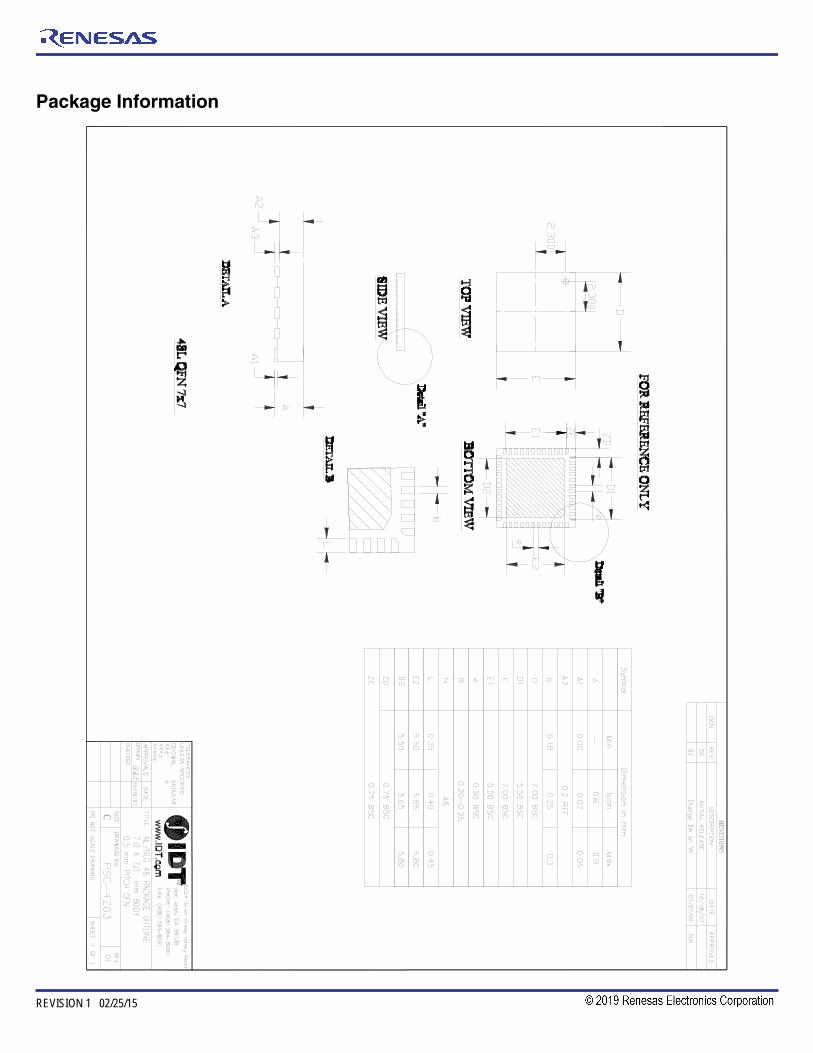
Package Information

8V44N4614 DATA SHEET
FEMTOCLOCK® NG JITTER ATTENUATOR AND CLOCK SYNTHESIZER 30 REVISION 1 02/25/15
Ordering Information
Marking Package Shipping Packaging Temperature
8V44N4614NLGI IDT8V44N4614NLGI 48 Lead VFQFN, Lead-Free Tray -40°C to +85°C
8V44N4614NLGI8 IDT8V44N4614NLGI 48 Lead VFQFN, Lead-FreeTape & Reel, Pin 1
Orientation: EIA-481-C-40C to 85C
8V44N4614NLGI/W IDT8V44N4614NLGI 48 Lead VFQFN, Lead-FreeTape & Reel, Pin 1
Orientation: EIA-481-D-40C to 85C
NOTE: Parts that are ordered with an “G” suffix to the part number are the Pb-Free configuration and are RoHS compliant.
Table 10. Pin 1 Orientation in Tape and Reel Packaging
Table 9. Ordering Information
Part/Order Number
Part Number Suffix Pin 1 Orientation Illustration
8 Quadrant 1 (EIA-481-C)
/W Quadrant 2 (EIA-481-D)

DISCLAIMER Integrated Device Technology, Inc. (IDT) and its subsidiaries reserve the right to modify the products and/or specifications described herein at any time and at IDT’s sole discretion. All information in this document, including descriptions of product features and performance, is subject to change without notice. Performance specifications and the operating parameters of the described products are determined in the independent state and are not guaranteed to perform the same way when installed in customer products. The information contained herein is provided without representation or warranty of any kind, whether express or implied, including, but not limited to, the suitability of IDT’s products for any particular purpose, an implied warranty of merchantability, or non-infringement of the intellectual property rights of others. This document is presented only as a guide and does not convey any license under intellectual property rights of IDT or any third parties.
IDT’s products are not intended for use in applications involving extreme environmental conditions or in life support systems or similar devices where the failure or malfunction of an IDT product can be reasonably expected to significantly affect the health or safety of users. Anyone using an IDT product in such a manner does so at their own risk, absent an express, written agreement by IDT.
Integrated Device Technology, IDT and the IDT logo are registered trademarks of IDT. Product specification subject to change without notice. Other trademarks and service marks used herein, including protected names, logos and designs, are the property of IDT or their respective third party owners.
Copyright ©2015 Integrated Device Technology, Inc.. All rights reserved.
Corporate Headquarters6024 Silver Creek Valley Road San Jose, CA 95138 USA
Sales1-800-345-7015 or 408-284-8200 Fax: 408-284-2775www.IDT.com
Tech Supportemail: [email protected]

Corporate HeadquartersTOYOSU FORESIA, 3-2-24 Toyosu,Koto-ku, Tokyo 135-0061, Japanwww.renesas.com
Contact InformationFor further information on a product, technology, the most up-to-date version of a document, or your nearest sales office, please visit:www.renesas.com/contact/
TrademarksRenesas and the Renesas logo are trademarks of Renesas Electronics Corporation. All trademarks and registered trademarks are the property of their respective owners.
IMPORTANT NOTICE AND DISCLAIMER
RENESAS ELECTRONICS CORPORATION AND ITS SUBSIDIARIES (“RENESAS”) PROVIDES TECHNICAL SPECIFICATIONS AND RELIABILITY DATA (INCLUDING DATASHEETS), DESIGN RESOURCES (INCLUDING REFERENCE DESIGNS), APPLICATION OR OTHER DESIGN ADVICE, WEB TOOLS, SAFETY INFORMATION, AND OTHER RESOURCES “AS IS” AND WITH ALL FAULTS, AND DISCLAIMS ALL WARRANTIES, EXPRESS OR IMPLIED, INCLUDING, WITHOUT LIMITATION, ANY IMPLIED WARRANTIES OF MERCHANTABILITY, FITNESS FOR A PARTICULAR PURPOSE, OR NON-INFRINGEMENT OF THIRD PARTY INTELLECTUAL PROPERTY RIGHTS.
These resources are intended for developers skilled in the art designing with Renesas products. You are solely responsible for (1) selecting the appropriate products for your application, (2) designing, validating, and testing your application, and (3) ensuring your application meets applicable standards, and any other safety, security, or other requirements. These resources are subject to change without notice. Renesas grants you permission to use these resources only for development of an application that uses Renesas products. Other reproduction or use of these resources is strictly prohibited. No license is granted to any other Renesas intellectual property or to any third party intellectual property. Renesas disclaims responsibility for, and you will fully indemnify Renesas and its representatives against, any claims, damages, costs, losses, or liabilities arising out of your use of these resources. Renesas' products are provided only subject to Renesas' Terms and Conditions of Sale or other applicable terms agreed to in writing. No use of any Renesas resources expands or otherwise alters any applicable warranties or warranty disclaimers for these products.
(Rev.1.0 Mar 2020)
© 2020 Renesas Electronics Corporation. All rights reserved.