fan7528 dual output critical conduction mode pfc · pdf file · 2009-02-24an7528...
TRANSCRIPT

©2006 Fairchild Semiconductor Corporation
1
www.fairchildsemi.com
March 2006
FAN7528 Rev. 1.0.4
FAN
7528 Du
al Ou
tpu
t Critical C
on
du
ction
Mo
de P
FC
Co
ntro
ller
FAN7528Dual Output Critical Conduction Mode PFC Controller
Features
■
Low Total Harmonic Distortion (THD)
■
Dual Output Voltage Control
■
Precise Adjustable Output Over Voltage Protection
■
Open-feedback Protection and Disable Function
■
Zero Current Detector
■
160µs Internal Start-up Timer
■
MOSFET Over Current Protection
■
Under Voltage Lock Out with 3.5V Hysteresis
■
Low Start-up (40µA) and Operating Current (1.5mA)
■
Totem Pole Output with High State Clamp
■
±
400mA Peak Gate Drive Current
■
8-pin DIP or 8-pin SOP
Applications
■
Adapter
Related Application Notes
■
AN6012
: Design of Power Factor Correction Circuit Using FAN7528
Description
The FAN7528 is an active power factor correction (PFC)controller for boost PFC applications which operates inthe critical conduction mode (CRM). It uses the voltagemode PWM that compares an internal ramp signal withthe error amplifier output to generate MOSFET turn-offsignal. Because the voltage mode CRM PFC controllerdoes not need the rectified AC line voltage information, itcan save the power loss of the input voltage sensing net-work that is necessary for the current mode CRM PFCcontroller.
The FAN7528 provides the dual output voltage controlfunction without the AC line voltage sensing for adapterapplications. It changes the PFC output voltage accord-ing to the AC line voltage.
It provides many protection functions such as over volt-age protection, open-feedback protection, over currentprotection and under voltage lock out protection. TheFAN7528 can be disabled if the INV pin voltage is lowerthan 0.45V and then the operating current decreases to65µA. Using a new variable on-time control method, THDis lower than the conventional CRM boost PFC ICs.
Ordering Information
Part NumberOperating Temp.
Range Pb-Free Package Packing MethodMarking
Code
FAN7528N -40
°
C to +125
°
C Yes 8-DIP Rail FAN7528
FAN7528M -40
°
C to +125
°
C Yes 8-SOP Rail FAN7528
FAN7528MX -40
°
C to +125
°
C Yes 8-SOP Tape & Reel FAN7528

2
www.fairchildsemi.com
FAN7528 Rev. 1.0.4
FAN
7528 Du
al Ou
tpu
t Critical C
on
du
ction
Mo
de P
FC
Co
ntro
ller
Typical Application Diagrams
Figure 1. Typical Boost PFC Application
Internal Block Diagram
Figure 2. Functional Block Diagram of FAN7528
GND
ZCD
INVVcc
ACIn
Vo
COMPCS
MOTFAN7528
R1
R2
L D
Co
NAUXVAUX
RZCD
INV
ErrorAmplif ier
OVP
COMP
8pF40k
2.5VRef
InternalBias
160µsTimer
Vcc
ZCD
CS
UVLO
6.7V
12V 8.5V
2.66V 2.55V
OCPComparator
1V Offset
MOT
GND
Saw ToothGenerator
Zero CurrentDetector
R
S
Q
3
6
4
5
2
1
8
Dual Output ReferenceGenerator1.5V/2.5V
Gm
Vref
0.8V
Disable
0.45V 0.35VDisable
1.5V1.4V
7
Vcc
OUTDriveOutput
13V
Vcc=8.5V Reference SetVcc=4.5V Reference Reset
RampSignal
1V~5VRange

3
www.fairchildsemi.com
FAN7528 Rev. 1.0.4
FAN
7528 Du
al Ou
tpu
t Critical C
on
du
ction
Mo
de P
FC
Co
ntro
ller
Pin Assignments
Figure 3. Pin Configuration (Top View)
Pin Definitions
Pin Number Pin Name Pin Function Description
1 INV This pin is the inverting input of the error amplifier. The output voltage of the boost PFC converter should be resistively divided to 2.5V at the high line condition and connected to this pin. If this pin voltage is controlled to be lower than 0.45V, the device is disabled.
2 COMP This pin is the output of the transconductance error amplifier. Some components for the output voltage compensation should be connected between this pin and GND.
3 MOT This pin is used to set the slope of the internal ramp. The voltage of this pin is maintained to be 1V. If a resistor is connected between this pin and GND, current flows out of the pin and the slope of the internal ramp is proportional to this current.
4 CS This pin is the input of the over current protection comparator. The MOSFET current is sensed using a sensing resistor and the resulting voltage is applied to this pin. An internal RC filter is included to filter switching noise. This pin is sensitive to the negative voltage below -0.3V. For proper operation, the stray inductance in the sensing path and the inductance of the sensing resistor must be minimized.
5 ZCD This pin is the input of the zero current detection block. If the voltage of this pin goes higher than 1.5V and then goes lower than 1.4V, the MOSFET is turned on.
6 GND This pin is used for the ground potential of all the pins. For proper operation, the signal ground and the power ground should be separated.
7 OUT This pin is the gate drive output. The peak sourcing and sinking current level is 400mA. For proper operation, the stray inductance in the gate driving path must be minimized.
8 Vcc This pin is the IC supply pin. IC current and MOSFET drive current are supplied using this pin.
FAN7528
6 58 7Vcc OUT GND ZCD
1 2 3 4
COMP CSMOTINV
WWW
4
www.fairchildsemi.com
FAN7528 Rev. 1.0.4
FAN
7528 Du
al Ou
tpu
t Critical C
on
du
ction
Mo
de P
FC
Co
ntro
ller
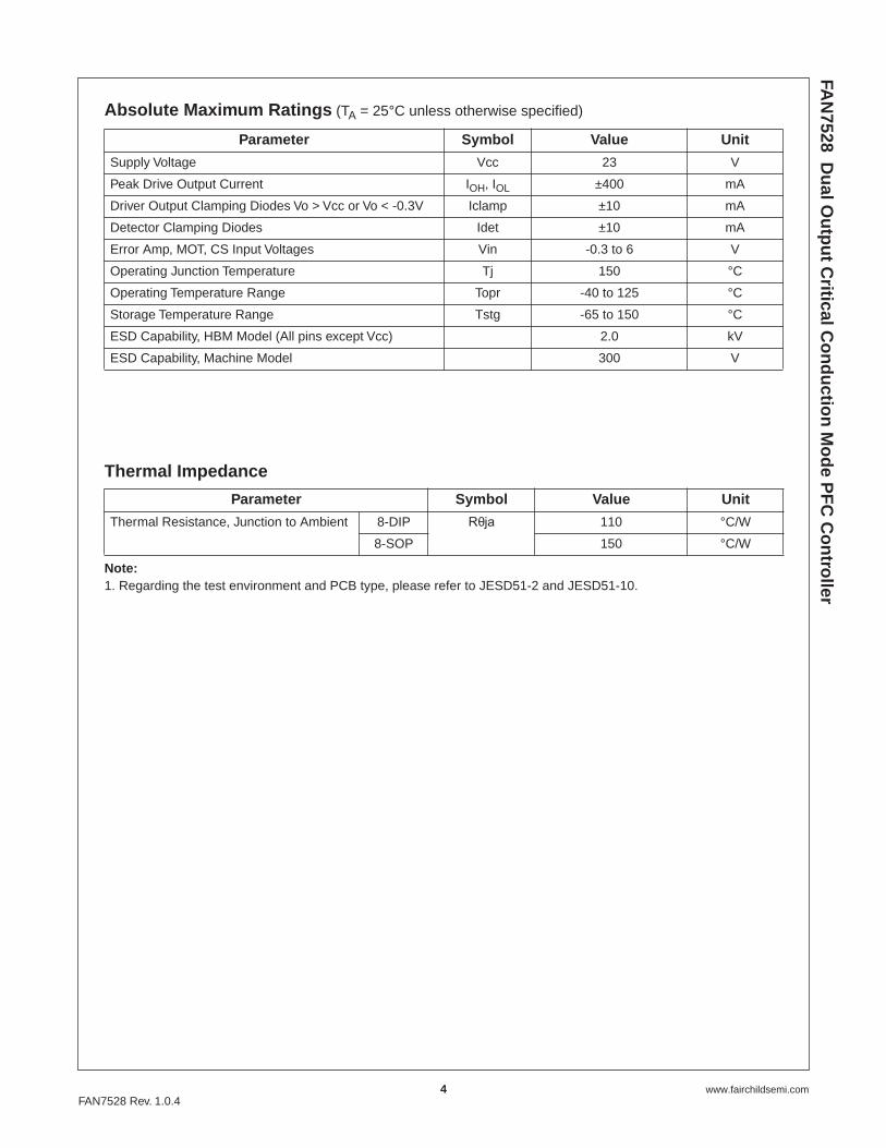
Absolute Maximum Ratings
(T
A
= 25°C unless otherwise specified)
Thermal Impedance
Note:
1. Regarding the test environment and PCB type, please refer to JESD51-2 and JESD51-10.
Parameter Symbol Value Unit
Supply Voltage Vcc 23 V
Peak Drive Output Current I
OH
, I
OL
±
400 mA
Driver Output Clamping Diodes Vo > Vcc or Vo < -0.3V Iclamp
±
10 mA
Detector Clamping Diodes Idet
±
10 mA
Error Amp, MOT, CS Input Voltages Vin -0.3 to 6 V
Operating Junction Temperature Tj 150
°
C
Operating Temperature Range Topr -40 to 125
°
C
Storage Temperature Range Tstg -65 to 150
°
C
ESD Capability, HBM Model (All pins except Vcc) 2.0 kV
ESD Capability, Machine Model 300 V
Parameter Symbol Value Unit
Thermal Resistance, Junction to Ambient 8-DIP
R
θ
ja
110
°
C/W
8-SOP 150
°
C/W

5
www.fairchildsemi.com
FAN7528 Rev. 1.0.4
FAN
7528 Du
al Ou
tpu
t Critical C
on
du
ction
Mo
de P
FC
Co
ntro
ller
Electrical Characteristics
(Vcc = 14V, T
A
= -40
°
C~125
°
C, unless otherwise specified)
Parameter Symbol Condition Min. Typ. Max. Unit
Under Voltage Lock Out Section
Start Threshold Voltage Vth(start) Vcc increasing 11 12 13 V
Stop Threshold Voltage Vth(stop) Vcc decreasing 8 8.5 9 V
UVLO Hysteresis HY(uvlo) 3 3.5 4 V
Supply Current Section
Start-up Supply Current Ist Vcc = Vth(start) – 0.2V – 40 70
µ
A
Operating Supply Current Icc Output no switching – 1.5 3 mA
Dynamic Operating Supply Current Idcc 50kHz, Cl=1nF – 2.5 4 mA
Operating Current at Disable Icc(dis) Vinv = 0V 40 65 90
µ
A
Error Amplifier Section
Voltage Feedback Input Threshold1
Vref1 Ta = 25
°
C 2.465 2.5 2.535 V
2.435 2.5 2.565 V
Voltage Feedback Input Threshold2 Vref2 1.45 1.5 1.55 V
Line Regulation
∆
V
ref1
Vcc = 14V~23V – 0.1 10 mV
Temperature Stability of Vref1
(1)
∆
V
ref3
– 20 – mV
Input Bias Current Ib(ea) Vinv = 1V~4V -0.5 – 0.5
µ
A
Output Source Current Isource Vinv = 2.4V – -12 –
µ
A
Output Sink Current Isink Vinv = 2.6V – 12 –
µ
A
Output Upper Clamp Voltage Veao(H) 4.5 5.5 6.5 V
Zero Duty Cycle Output Voltage Veao(Z) 0.7 1 1.3 V
Transconductance
(1)
gm 90 115 140
µ
mho
Output Voltage Selection Threshold Vth(in) T
A
= 25
°
C 1.24 1.3 1.36 V
Output Voltage Reset Threshold
(1)
Vth(reset) 3 4.5 6 V
Maximum On-Time Section
Maximum On-time Voltage Vmot Rmot = 13.7k 0.95 1 1.05 V
Maximum On-time Programming Ton-max Rmot = 13.7k, T
A
= 25
°
C 18 22.5 27
µ
s
Current Sense Section
Current Sense Input Threshold Voltage Limit
Vcs(limit) 0.7 0.8 0.9 V
Input Bias Current Ib(cs) Vcs = 0V~1V -1 -0.1 1
µ
A
Current Sense Delay to Output
(1)
Td(cs) – 350 500 ns
6
www.fairchildsemi.com
FAN7528 Rev. 1.0.4
FAN
7528 Du
al Ou
tpu
t Critical C
on
du
ction
Mo
de P
FC
Co
ntro
ller
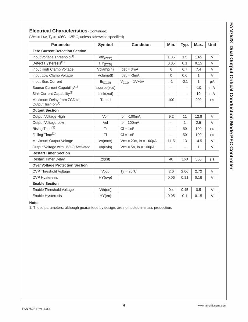
Electrical Characteristics
(Continued)
(Vcc = 14V, T
A
= -40
°
C~125
°
C, unless otherwise specified)
Note:
1. These parameters, although guaranteed by design, are not tested in mass production.
Parameter Symbol Condition Min. Typ. Max. Unit
Zero Current Detection Section
Input Voltage Threshold
(1)
Vth
(ZCD)
1.35 1.5 1.65 V
Detect Hysteresis
(1)
HY
(ZCD)
0.05 0.1 0.15 V
Input High Clamp Voltage Vclamp(h) Idet = 3mA 6 6.7 7.4 V
Input Low Clamp Voltage Vclamp(l) Idet = -3mA 0 0.6 1 V
Input Bias Current Ib
(ZCD)
V
ZCD
= 1V~5V -1 -0.1 1
µ
A
Source Current Capability
(1)
Isource(zcd) – – -10 mA
Sink Current Capability
(1)
Isink(zcd) – – 10 mA
Maximum Delay from ZCD to Output Turn-on
(1)
Tdead 100 – 200 ns
Output Section
Output Voltage High Voh Io = -100mA 9.2 11 12.8 V
Output Voltage Low Vol Io = 100mA – 1 2.5 V
Rising Time
(1)
Tr Cl = 1nF – 50 100 ns
Falling Time
(1)
Tf Cl = 1nF – 50 100 ns
Maximum Output Voltage Vo(max) Vcc = 20V, Io = 100
µ
A 11.5 13 14.5 V
Output Voltage with UVLO Activated Vo(uvlo) Vcc = 5V, Io = 100
µ
A – – 1 V
Restart Timer Section
Restart Timer Delay td(rst) 40 160 360
µ
s
Over Voltage Protection Section
OVP Threshold Voltage Vovp T
A
= 25
°
C 2.6 2.66 2.72 V
OVP Hysteresis HY(ovp) 0.06 0.11 0.16 V
Enable Section
Enable Threshold Voltage Vth(en) 0.4 0.45 0.5 V
Enable Hysteresis HY(en) 0.05 0.1 0.15 V
7
www.fairchildsemi.com
FAN7528 Rev. 1.0.4
FAN
7528 Du
al Ou
tpu
t Critical C
on
du
ction
Mo
de P
FC
Co
ntro
ller
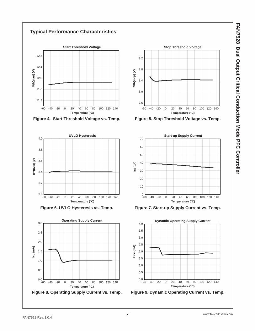
Typical Performance Characteristics
Figure 4. Start Threshold Voltage vs. Temp. Figure 5. Stop Threshold Voltage vs. Temp.
Figure 6. UVLO Hysteresis vs. Temp. Figure 7. Start-up Supply Current vs. Temp.
Figure 8. Operating Supply Current vs. Temp. Figure 9. Dynamic Operating Current vs. Temp.
Start Threshold Voltage
Temperature (°C)
Vth
(sta
rt)
(V)
-60 -40
12.8
12.4
12.0
11.6
11.2
-20 0 20 40 60 80 100 120 140
Stop Threshold Voltage
Temperature (°C)
Vth
(sto
p)
(V)
-60 -40
9.2
8.8
8.4
8.0
7.6
-20 0 20 40 60 80 100 120 140
Start-up Supply Current
Temperature (°C)
Ist
(µA
)
-60 -40
70
60
50
40
30
20
10
0-20 0 20 40 60 80 100 120 140
UVLO Hysteresis
Temperature (°C)
HY
(uvl
o)
(V)
-60 -40
4.0
3.8
3.6
3.4
3.2
3.0-20 0 20 40 60 80 100 120 140
Operating Supply Current
Temperature (°C)
Icc
(mA
)
-60 -40
3.0
2.5
2.0
1.5
1.0
0.5
0.0-20 0 20 40 60 80 100 120 140
Dynamic Operating Supply Current
Temperature (°C)
Idcc
(m
A)
-60 -40
4.0
3.5
3.0
2.5
2.0
1.5
1.0
0.5
0.0-20 0 20 40 60 80 100 120 140

8 www.fairchildsemi.comFAN7528 Rev. 1.0.4
FAN
7528 Du
al Ou
tpu
t Critical C
on
du
ction
Mo
de P
FC
Co
ntro
ller
Typical Performance Characteristics (Continued)
Figure 10. Icc at Disable vs. Temp. Figure 11. Vref1 vs. Temp.
Figure 12. Vref2 vs. Temp. Figure 13. Input Bias Current vs. Temp.
Figure 14. Error Amp. Source Current vs. Temp. Figure 15. Error Amp. Sink Current vs. Temp.
Operating Current at Disable
Temperature (°C)
Icc(
dis
) (µ
A)
-60 -40
90
80
70
60
50
40-20 0 20 40 60 80 100 120 140
Voltage Feedback Input Threshold1
Temperature (°C)
Vre
f1 (
V)
-60 -40
2.56
2.54
2.52
2.50
2.48
2.46
2.44
-20 0 20 40 60 80 100 120 140
Voltage Feedback Input Threshold2
Temperature (°C)
Vre
f2 (
V)
-60 -40
1.54
1.52
1.50
1.48
1.46
-20 0 20 40 60 80 100 120 140
Input Bias Current
Temperature (°C)
Ib(e
a) (
µA)
-60 -40
0.4
0.2
0.0
-0.2
-0.4
-20 0 20 40 60 80 100 120 140
Output Source Current
Temperature (°C)
Iso
urc
e (µ
A)
-60 -40
-6
-9
-12
-15
-18
-20 0 20 40 60 80 100 120 140
Output Sink Current
Temperature (°C)
Isin
k (µ
A)
-60 -40
18
15
12
9
6
-20 0 20 40 60 80 100 120 140

9 www.fairchildsemi.comFAN7528 Rev. 1.0.4
FAN
7528 Du
al Ou
tpu
t Critical C
on
du
ction
Mo
de P
FC
Co
ntro
ller
Typical Performance Characteristics (Continued)
Figure 16. Error Amp. Clamp Voltage vs. Temp. Figure 17. Zero Duty Output Voltage vs. Temp.
Figure 18. Output Select Threshold vs. Temp. Figure 19. MOT pin Voltage vs. Temp.
Figure 20. Maximum On-time vs. Temp. Figure 21. Current Limit vs. Temp.
Output Upper Clamp Voltage
Temperature (°C)
Vea
o(H
) (V
)
-60 -40
6.5
6.0
5.5
5.0
4.5-20 0 20 40 60 80 100 120 140
Zero Duty Cycle Output Voltage
Temperature (°C)
Vea
o(Z
) (V
)
-60 -40
1.3
1.2
1.1
1.0
0.9
0.8
0.7-20 0 20 40 60 80 100 120 140
Output Voltage Selection Threshold
Temperature (°C)
Vth
(in
) (V
)
-60 -40
1.36
1.34
1.32
1.30
1.28
1.26
1.24-20 0 20 40 60 80 100 120 140
Maximum On-Time Voltage
Temperature (°C)
Vm
ot
(V)
-60 -40
1.04
1.02
1.00
0.98
0.96
-20 0 20 40 60 80 100 120 140
Maximum On-Time Programming
Temperature (°C)
To
n-m
ax (
µs)
-60 -40
26
24
22
20
18-20 0 20 40 60 80 100 120 140
Current Sense Input Threshold Voltage
Temperature (°C)
Vcs
(lim
it)
(V)
-60 -40
0.88
0.84
0.80
0.76
0.72
-20 0 20 40 60 80 100 120 140
10 www.fairchildsemi.comFAN7528 Rev. 1.0.4
FAN
7528 Du
al Ou
tpu
t Critical C
on
du
ction
Mo
de P
FC
Co
ntro
ller
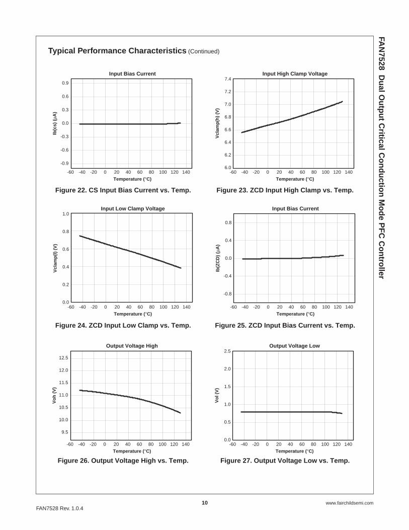
Typical Performance Characteristics (Continued)
Figure 22. CS Input Bias Current vs. Temp. Figure 23. ZCD Input High Clamp vs. Temp.
Figure 24. ZCD Input Low Clamp vs. Temp. Figure 25. ZCD Input Bias Current vs. Temp.
Figure 26. Output Voltage High vs. Temp. Figure 27. Output Voltage Low vs. Temp.
Input Bias Current
Temperature (°C)
Ib(c
s) (
µA)
-60 -40
0.9
0.6
0.3
0.0
-0.3
-0.6
-0.9
-20 0 20 40 60 80 100 120 140
Input High Clamp Voltage
Temperature (°C)
Vcl
amp
(h)
(V)
-60 -40
7.4
7.2
7.0
6.8
6.6
6.4
6.2
6.0-20 0 20 40 60 80 100 120 140
Input Low Clamp Voltage
Temperature (°C)
Vcl
amp
(l)
(V)
-60 -40
1.0
0.8
0.6
0.4
0.2
0.0-20 0 20 40 60 80 100 120 140
Input Bias Current
Temperature (°C)
Ib(Z
CD
) (µ
A)
-60 -40
0.8
0.4
0.0
-0.4
-0.8
-20 0 20 40 60 80 100 120 140
Output Voltage High
Temperature (°C)
Vo
h (
V)
-60 -40
12.5
12.0
11.5
11.0
10.5
10.0
9.5
-20 0 20 40 60 80 100 120 140
Output Voltage Low
Temperature (°C)
Vo
l (V
)
-60 -40
2.5
2.0
1.5
1.0
0.5
0.0-20 0 20 40 60 80 100 120 140
11 www.fairchildsemi.comFAN7528 Rev. 1.0.4
FAN
7528 Du
al Ou
tpu
t Critical C
on
du
ction
Mo
de P
FC
Co
ntro
ller
Typical Performance Characteristics (Continued)
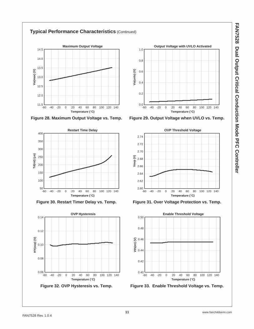
Figure 28. Maximum Output Voltage vs. Temp. Figure 29. Output Voltage when UVLO vs. Temp.
Figure 30. Restart Timer Delay vs. Temp. Figure 31. Over Voltage Protection vs. Temp.
Figure 32. OVP Hysteresis vs. Temp. Figure 33. Enable Threshold Voltage vs. Temp.
Maximum Output Voltage
Temperature (°C)
Vo
(max
) (V
)
-60 -40
14.5
14.0
13.5
13.0
12.5
12.0
11.5-20 0 20 40 60 80 100 120 140
Output Voltage with UVLO Activated
Temperature (°C)
Vo
(uvl
o)
(V)
-60 -40
1.0
0.8
0.6
0.4
0.2
0.0-20 0 20 40 60 80 100 120 140
Restart Time Delay
Temperature (°C)
Td
(rst
) (µ
s)
-60 -40
400
350
300
250
200
150
100
50-20 0 20 40 60 80 100 120 140
OVP Threshold Voltage
Temperature (°C)
Vo
vp (
V)
-60 -40
2.74
2.72
2.70
2.68
2.66
2.64
2.62
2.60-20 0 20 40 60 80 100 120 140
OVP Hysteresis
Temperature (°C)
HY
(ovp
) (V
)
-60 -40
0.14
0.12
0.10
0.08
0.06-20 0 20 40 60 80 100 120 140
Enable Threshold Voltage
Temperature (°C)
Vth
(en
) (V
)
-60 -40
0.50
0.48
0.46
0.44
0.42
0.40-20 0 20 40 60 80 100 120 140

12 www.fairchildsemi.comFAN7528 Rev. 1.0.4
FAN
7528 Du
al Ou
tpu
t Critical C
on
du
ction
Mo
de P
FC
Co
ntro
ller
Typical Performance Characteristics (Continued)
Figure 34. Enable Hysteresis vs. Temp.
Enable Hysteresis
Temperature (°C)
HY
(en
) (V
)
-60 -40
0.14
0.12
0.10
0.08
0.06
-20 0 20 40 60 80 100 120 140
13 www.fairchildsemi.comFAN7528 Rev. 1.0.4
FAN
7528 Du
al Ou
tpu
t Critical C
on
du
ction
Mo
de P
FC
Co
ntro
ller
Applications Information
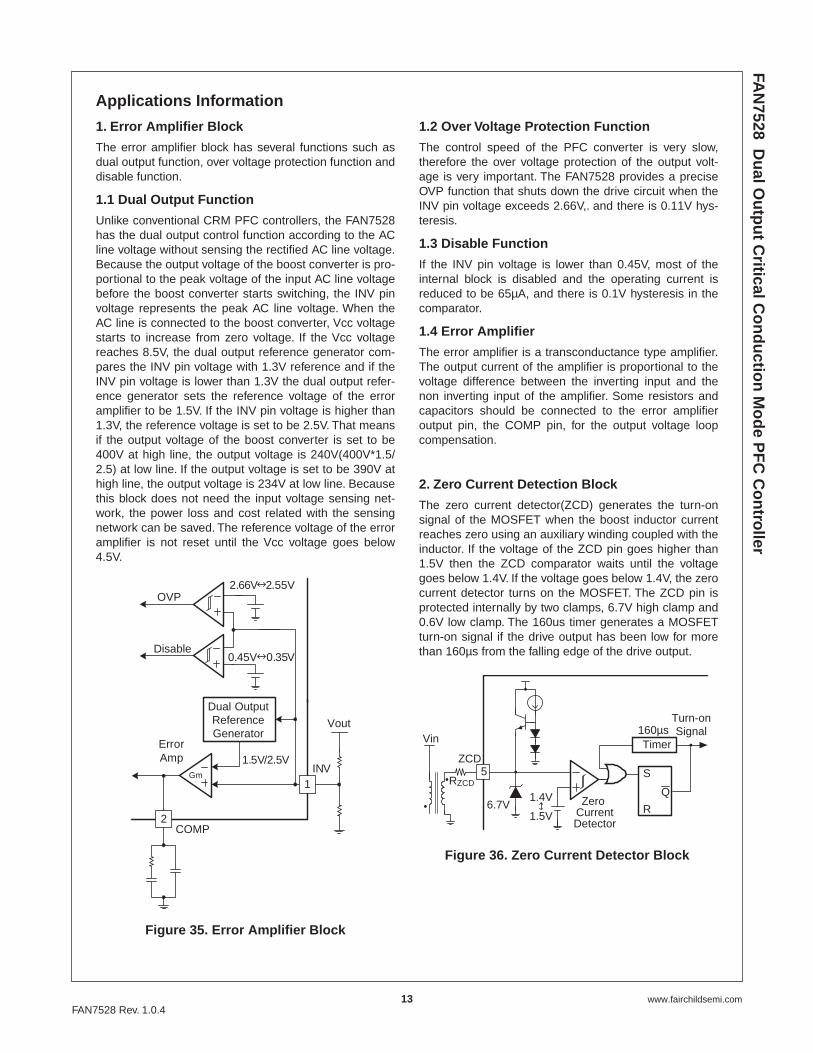
1. Error Amplifier Block
The error amplifier block has several functions such asdual output function, over voltage protection function anddisable function.
1.1 Dual Output Function
Unlike conventional CRM PFC controllers, the FAN7528has the dual output control function according to the ACline voltage without sensing the rectified AC line voltage.Because the output voltage of the boost converter is pro-portional to the peak voltage of the input AC line voltagebefore the boost converter starts switching, the INV pinvoltage represents the peak AC line voltage. When theAC line is connected to the boost converter, Vcc voltagestarts to increase from zero voltage. If the Vcc voltagereaches 8.5V, the dual output reference generator com-pares the INV pin voltage with 1.3V reference and if theINV pin voltage is lower than 1.3V the dual output refer-ence generator sets the reference voltage of the erroramplifier to be 1.5V. If the INV pin voltage is higher than1.3V, the reference voltage is set to be 2.5V. That meansif the output voltage of the boost converter is set to be400V at high line, the output voltage is 240V(400V*1.5/2.5) at low line. If the output voltage is set to be 390V athigh line, the output voltage is 234V at low line. Becausethis block does not need the input voltage sensing net-work, the power loss and cost related with the sensingnetwork can be saved. The reference voltage of the erroramplifier is not reset until the Vcc voltage goes below4.5V.
Figure 35. Error Amplifier Block
1.2 Over Voltage Protection Function
The control speed of the PFC converter is very slow,therefore the over voltage protection of the output volt-age is very important. The FAN7528 provides a preciseOVP function that shuts down the drive circuit when theINV pin voltage exceeds 2.66V,. and there is 0.11V hys-teresis.
1.3 Disable Function
If the INV pin voltage is lower than 0.45V, most of theinternal block is disabled and the operating current isreduced to be 65µA, and there is 0.1V hysteresis in thecomparator.
1.4 Error Amplifier
The error amplifier is a transconductance type amplifier.The output current of the amplifier is proportional to thevoltage difference between the inverting input and thenon inverting input of the amplifier. Some resistors andcapacitors should be connected to the error amplifieroutput pin, the COMP pin, for the output voltage loopcompensation.
2. Zero Current Detection Block
The zero current detector(ZCD) generates the turn-onsignal of the MOSFET when the boost inductor currentreaches zero using an auxiliary winding coupled with theinductor. If the voltage of the ZCD pin goes higher than1.5V then the ZCD comparator waits until the voltagegoes below 1.4V. If the voltage goes below 1.4V, the zerocurrent detector turns on the MOSFET. The ZCD pin isprotected internally by two clamps, 6.7V high clamp and0.6V low clamp. The 160us timer generates a MOSFETturn-on signal if the drive output has been low for morethan 160µs from the falling edge of the drive output.
Figure 36. Zero Current Detector Block
OVP2.66V 2.55V
0.45V 0.35VDisable
INV
ErrorAmp
COMP2
1Gm
Dual OutputReferenceGenerator
Vout
1.5V/2.5VTimer
ZCD
6.7V Zero CurrentDetector
R
S
Q
5
1.4V
1.5V
Turn-onSignal
Vin
RZCD
160µs
14 www.fairchildsemi.comFAN7528 Rev. 1.0.4
FAN
7528 Du
al Ou
tpu
t Critical C
on
du
ction
Mo
de P
FC
Co
ntro
ller
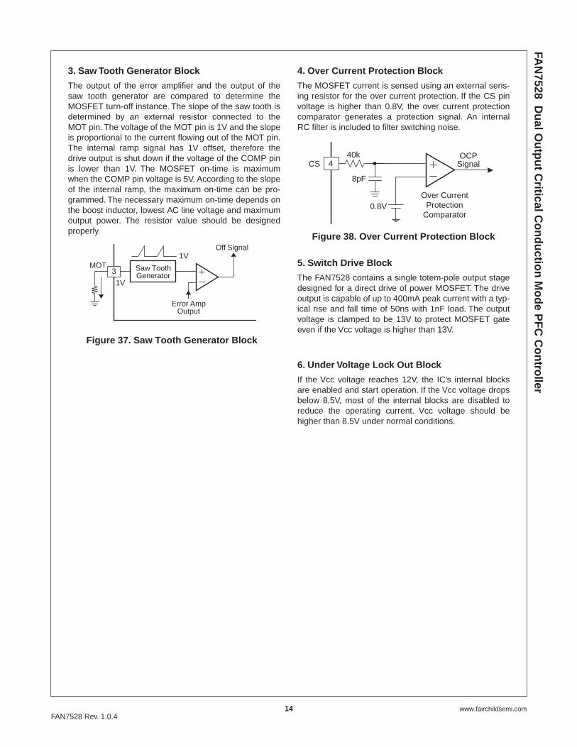
3. Saw Tooth Generator Block
The output of the error amplifier and the output of thesaw tooth generator are compared to determine theMOSFET turn-off instance. The slope of the saw tooth isdetermined by an external resistor connected to theMOT pin. The voltage of the MOT pin is 1V and the slopeis proportional to the current flowing out of the MOT pin.The internal ramp signal has 1V offset, therefore thedrive output is shut down if the voltage of the COMP pinis lower than 1V. The MOSFET on-time is maximumwhen the COMP pin voltage is 5V. According to the slopeof the internal ramp, the maximum on-time can be pro-grammed. The necessary maximum on-time depends onthe boost inductor, lowest AC line voltage and maximumoutput power. The resistor value should be designedproperly.
Figure 37. Saw Tooth Generator Block
4. Over Current Protection Block
The MOSFET current is sensed using an external sens-ing resistor for the over current protection. If the CS pinvoltage is higher than 0.8V, the over current protectioncomparator generates a protection signal. An internalRC filter is included to filter switching noise.
Figure 38. Over Current Protection Block
5. Switch Drive Block
The FAN7528 contains a single totem-pole output stagedesigned for a direct drive of power MOSFET. The driveoutput is capable of up to 400mA peak current with a typ-ical rise and fall time of 50ns with 1nF load. The outputvoltage is clamped to be 13V to protect MOSFET gateeven if the Vcc voltage is higher than 13V.
6. Under Voltage Lock Out Block
If the Vcc voltage reaches 12V, the IC’s internal blocksare enabled and start operation. If the Vcc voltage dropsbelow 8.5V, most of the internal blocks are disabled toreduce the operating current. Vcc voltage should behigher than 8.5V under normal conditions.
1VMOT Saw Tooth
Generator3
Error AmpOutput
Off Signal
1V
8pF
40kCS
Over CurrentProtection
Comparator
4
0.8V
OCPSignal

15 www.fairchildsemi.comFAN7528 Rev. 1.0.4
FAN
7528 Du
al Ou
tpu
t Critical C
on
du
ction
Mo
de P
FC
Co
ntro
ller
Typical Application Circuit
Features
■ High efficiency (>90% at 90 Vac input)■ Low THD (total harmonic distortion) (<10% at 264 Vac input)■ Dual output control
Key Design Notes
■ Diode D4 is used to prevent IC malfunction that can happen if the CS pin voltage is lower than -0.3V.■ Important Component s for low THD are R2, R5 and C11.
1. Schematic
Figure 39. Schematic
Application Output power Input voltage Output voltage
Adapter 100W Universal input(90~264 Vac)
389V/232V
F1
AC Input
5678
OU
T
Vcc
GN
D
ZC
D
INV
CO
MP
MO
T
CS
FAN7528
1 2 3 4
V1
C1
C3 C4
LF1C2
NTC
BD C5
R1C6
R3 R4 R5
T1
D1
C7R7
R10
R6
R8
D2
R9
C8
Q1
VAUX
R2
R11
C9
ZD1
C10
PFC Output
D3
D4
C11

16 www.fairchildsemi.comFAN7528 Rev. 1.0.4
FAN
7528 Du
al Ou
tpu
t Critical C
on
du
ction
Mo
de P
FC
Co
ntro
ller
2. Inductor Schematic Diagram
Figure 40. Inductor Schematic Diagram
3. Winding Specification
4. Electrical Characteristics
5. Core & Bobbin
■ Core: EI 3026■ Bobbin: EI3026■ Ae(mm2): 111
No Pin (s→f) Wire Turns Winding Method
NVcc 2 → 1 0.2φ × 1 6 Solenoid Winding
Insulation: Polyester Tape t = 0.050mm, 4 Layers
Np 5 → 3 0.2φ × 10 44 Solenoid Winding
Outer Insulation: Polyester Tape t = 0.050mm, 4Layers
Air Gap: 0.6mm for each leg
Pin Specification Remarks
Inductance 3–5 400µH ± 10% 100kHz, 1V
Np
1
2
NVcc
5
3

17 www.fairchildsemi.comFAN7528 Rev. 1.0.4
FAN
7528 Du
al Ou
tpu
t Critical C
on
du
ction
Mo
de P
FC
Co
ntro
ller
6. Demo Circuit Part List
Part Value Note Part Value Note
Fuse Inductor
F1 3A/250V T1 400µH EI3026
NTC
NTC 10D-9 MOSFET
Resistor Q1 FQPF13N50C Fairchild
R1 10k 1/4W
R2 370k 1/4W Diode
R3 330k 1/2W D1 1N4148 Fairchild
R4 150 1/2W D2 BYV26C 600V, 1A
R5 20k 1/4W D3 1N5819 Fairchild
R6 10 1/4W D4 1N5819 Fairchild
R7 0.22 1/2W ZD1 1N4746 18V
R8 10k 1/4W
R9 10k 1/4W Bridge Diode
R10 2M 1/4W BD KBL06 600V/4A
R11 12.9k 1/4W
Capacitor Line Filter
C1 150nF/275VAC Box Capacitor LF1 40mH Wire 0.4mm
C2 330nF/275VAC Box Capacitor
C3 2.2nF/3kV Ceramic Capacitor IC
C4 2.2nF/3kV Ceramic Capacitor IC1 FAN7528 Fairchild
C5 150nF/630V Film Capacitor
C6 47uF/25V Electrolytic Capacitor TNR
C7 47nF/50V Ceramic Capacitor V1 471 470V
C8 220nF MLCC
C9 100µF/450V Electrolytic Capacitor
C10 12nF/100V Film Capacitor
C11 47pF/50V Ceramic Capacitor
18 www.fairchildsemi.comFAN7528 Rev. 1.0.4
FAN
7528 Du
al Ou
tpu
t Critical C
on
du
ction
Mo
de P
FC
Co
ntro
ller
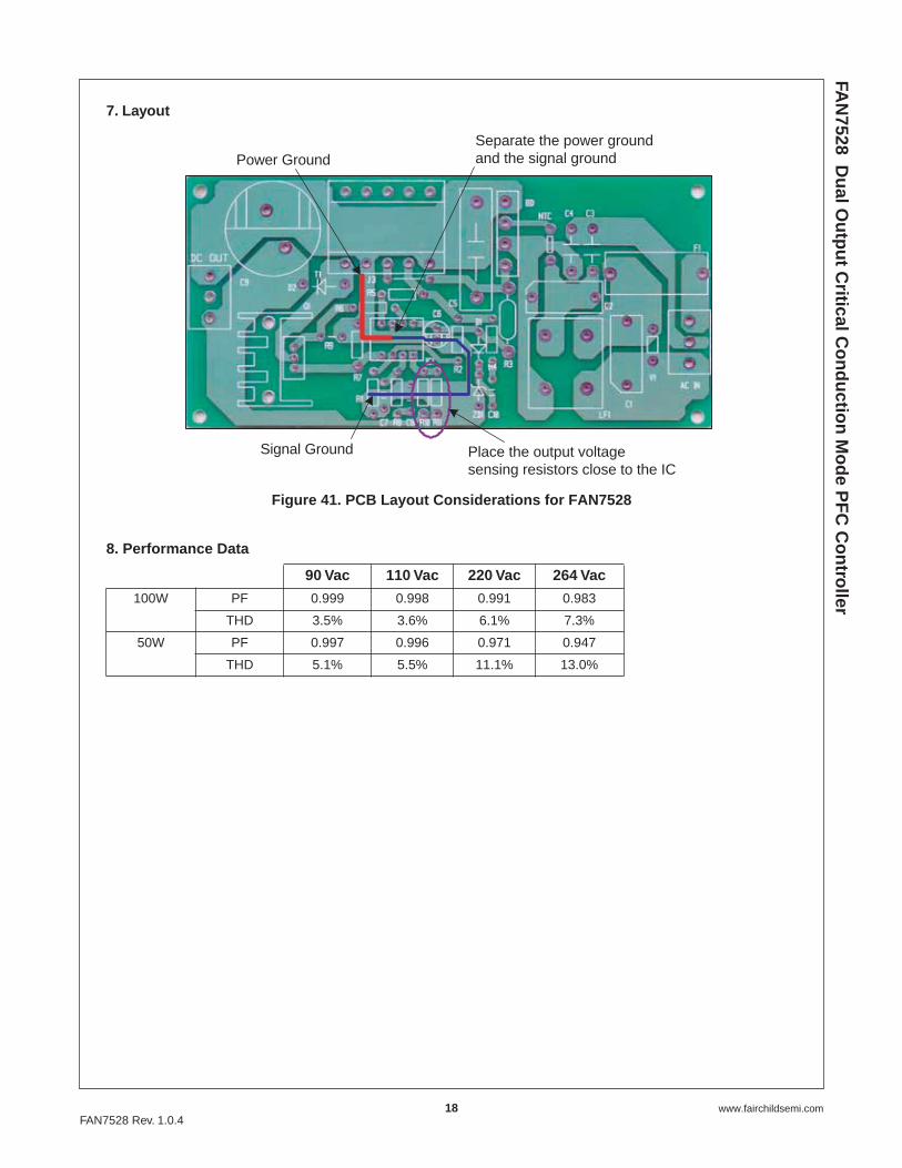
7. Layout
Figure 41. PCB Layout Considerations for FAN7528
8. Performance Data
90 Vac 110 Vac 220 Vac 264 Vac
100W PF 0.999 0.998 0.991 0.983
THD 3.5% 3.6% 6.1% 7.3%
50W PF 0.997 0.996 0.971 0.947
THD 5.1% 5.5% 11.1% 13.0%
Power Ground
Signal Ground Place the output voltagesensing resistors close to the IC
Separate the power ground and the signal ground
19 www.fairchildsemi.comFAN7528 Rev. 1.0.4
FAN
7528 Du
al Ou
tpu
t Critical C
on
du
ction
Mo
de P
FC
Co
ntro
ller
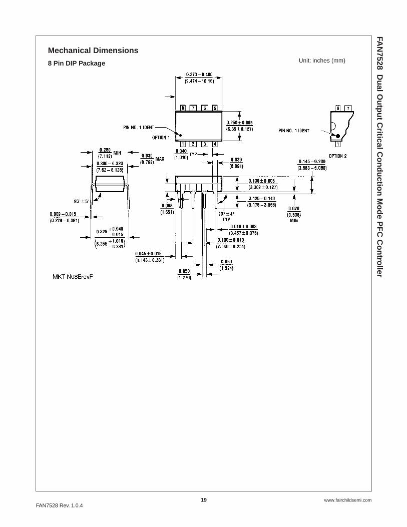
Mechanical Dimensions
8 Pin DIP Package Unit: inches (mm)

20 www.fairchildsemi.comFAN7528 Rev. 1.0.4
FAN
7528 Du
al Ou
tpu
t Critical C
on
du
ction
Mo
de P
FC
Co
ntro
ller
Mechanical Dimensions
8-Pin SOP Package Unit: mm
NOTES: UNLESS OTHERWISE SPECIFIED
A) THIS PACKAGE CONFORMS TO JEDEC MS-012, VARIATION AA, ISSUE C, DATED MAY 1990. B) ALL DIMENSIONS ARE IN MILLIMETERS. C) DIMENSIONS DO NOT INCLUDE MOLD FLASH OR BURRS. D) STANDARD LEAD FINISH: 200 MICROINCHES / 5.08 MICRONS MIN. LEAD/TIN (SOLDER) ON COPPER.
0.15+0.10-0.05
(R0.10)
0.70±0.20
(1.04)
1.75 MAX
1.45+0.05-0.20
(R0.10)
0.501.27
SEE DETAIL A
0.36
SEATING PLANE
0.10 C
C
GAGE PLANE
0.500.25 X 45°
3.81
0.250.19
1.00
6.75
4.75
(0.33)
1.27
6.00
PIN ONEINDICATOR
CM B A0.25
3.90±0.10
0.510.35
B
4.90±0.10
3.81
A
M08AREVK
LAND PATTERN RECOMMENDATION
DETAIL ASCALE: 2:1
4
8
1
5
8°0°
21 www.fairchildsemi.comFAN7528 Rev. 1.0.4
FAN
7528 Du
al Ou
tpu
t Critical C
on
du
ction
Mo
de P
FC
Co
ntro
ller
DISCLAIMER
FAIRCHILD SEMICONDUCTOR RESERVES THE RIGHT TO MAKE CHANGES WITHOUT FURTHER NOTICE TO ANYPRODUCTS HEREIN TO IMPROVE RELIABILITY, FUNCTION OR DESIGN. FAIRCHILD DOES NOT ASSUME ANY LIABILITYARISING OUT OF THE APPLICATION OR USE OF ANY PRODUCT OR CIRCUIT DESCRIBED HEREIN; NEITHER DOES ITCONVEY ANY LICENSE UNDER ITS PATENT RIGHTS, NOR THE RIGHTS OF OTHERS.
TRADEMARKS
The following are registered and unregistered trademarks Fairchild Semiconductor owns or is authorized to use and isnot intended to be an exhaustive list of all such trademarks.
LIFE SUPPORT POLICY
FAIRCHILDíS PRODUCTS ARE NOT AUTHORIZED FOR USE AS CRITICAL COMPONENTS IN LIFE SUPPORTDEVICES OR SYSTEMS WITHOUT THE EXPRESS WRITTEN APPROVAL OF FAIRCHILD SEMICONDUCTOR CORPORATION.As used herein:1. Life support devices or systems are devices orsystems which, (a) are intended for surgical implant intothe body, or (b) support or sustain life, or (c) whosefailure to perform when properly used in accordancewith instructions for use provided in the labeling, can bereasonably expected to result in significant injury to theuser.
2. A critical component is any component of a lifesupport device or system whose failure to perform canbe reasonably expected to cause the failure of the lifesupport device or system, or to affect its safety oreffectiveness.
PRODUCT STATUS DEFINITIONS
Definition of Terms
Datasheet Identification Product Status Definition
Advance Information
Preliminary
No Identification Needed
Obsolete
This datasheet contains the design specifications forproduct development. Specifications may change inany manner without notice.
This datasheet contains preliminary data, andsupplementary data will be published at a later date.Fairchild Semiconductor reserves the right to makechanges at any time without notice in order to improvedesign.
This datasheet contains final specifications. FairchildSemiconductor reserves the right to make changes atany time without notice in order to improve design.
This datasheet contains specifications on a productthat has been discontinued by Fairchild semiconductor.The datasheet is printed for reference information only.
Formative orIn Design
First Production
Full Production
Not In Production
ISOPLANAR™ LittleFET™
MICROCOUPLER™MicroFET™MicroPak™MICROWIRE™MSX™MSXPro™OCX™OCXPro™OPTOLOGIC®
OPTOPLANAR™PACMAN™POP™Power247™PowerEdge™
FAST®
FASTr™ FPS™
FRFET™GlobalOptoisolator™GTO™HiSeC™I2C™i-Lo™ImpliedDisconnect™IntelliMAX™
Rev. I18
ACEx™ActiveArray™Bottomless™Build it Now™CoolFET™CROSSVOLT™DOME™EcoSPARK™E2CMOS™EnSigna™FACT™FACT Quiet Series™
PowerSaver™PowerTrench®
QFET®
QS™QT Optoelectronics™Quiet Series™RapidConfigure™RapidConnect™µSerDes™ScalarPump™SILENT SWITCHER®
SMART START™SPM™Stealth™SuperFET™SuperSOT™-3
SuperSOT™-6SuperSOT™-8SyncFET™
TCM™ TinyLogic®
TINYOPTO™TruTranslation™UHC™UltraFET®
UniFET™VCX™Wire™
Across the board. Around the world.™The Power Franchise®
Programmable Active Droop™