failure modes and bonding strength of ultrasonically
TRANSCRIPT
Journal of Materials Processing Tech. 299 (2022) 117385
Available online 29 September 20210924-0136/© 2021 Elsevier B.V. All rights reserved.
Failure modes and bonding strength of ultrasonically-soldered glass joints
Jennifer Shaffer Brown , Caleb Wilson , Charles Bohlen , Hongseok Choi , Lonny Thompson , Joshua B. Bostwick * Department of Mechanical Engineering, Clemson University, Clemson, SC, 29634, United States
A R T I C L E I N F O
Associate Editor: S.-J. Na
Keywords: Ultrasonic-assisted soldering Active solder Solder joint quality Adhesion Process parameters
A B S T R A C T
While useful for optics and solar energy applications, solder-glass joints are difficult to fabricate due to poor wettability and adhesion, but reliable joints can be achieved with the use of ultrasonic-assisted soldering (UAS). In this study, an automated UAS system was used to investigate the effects of processing parameters on the solder joint quality so that the technology can be more suitably scaled for future widespread use in industry. Through mechanical shear strength testing of soldered joints and microstructure failure surface analysis with XRD, a more comprehensive understanding of the relationships between processing parameters and joint quality was devel-oped. Two novel failure surface types with distinct failure behavior were observed which could be predicted based on soldering tip speeds. The differences between the two failure surfaces appear to be due to the growth of a thin surface oxide layer on the solder lines from prolonged sonication, as determined from EDS and XRD microstructure analysis. These observations and analysis highlight a complex relationship that determines the quality of the solder-glass joint and suggest further research is necessary to refine the UAS process specifically for glass substrates and their varied applications in industry to prevent premature failure.
1. Introduction
As many industries continue to miniaturize electronics and other devices for portability and phase out use of environmentally harmful fluxes and lead-based solders due to growing legislative pressures across the globe, ultrasonic-assisted soldering (UAS) with lead-free solder al-loys has emerged as a suitable alternative to replace conventional sol-dering techniques. Studies by both Wilson et al. (2021) and Yonekura et al. (2015) have demonstrated that UAS is capable of enhancing the wettability of traditionally difficult-to-wet solder-substrate systems without the use of flux or the need for a protective inert atmosphere during the soldering process. This reduces the overall cost of manufacturing by eliminating the need for post-process removal of flux residues, which are known to embrittle the solder joints if they are not properly removed. The aim of the current work is to identify and better understand the parameters most strongly influencing the quality and reliability of ultrasonically soldered joints with silica glass substrates to prevent premature joint failure. The identification of the most influen-tial UAS processing parameters in this research study will help guide more effective quality control measures and better prepare this tech-nology for industrial-scale manufacturing.
UAS is a suitable match for many industrial applications, as it largely
negates the need for a protective inert atmosphere during the soldering process that conventional soldering practices require, without appre-ciably affecting solder joint strength for many solder-substrate systems. This facet of UAS has been demonstrated by Hashemabad et al. (2016) in an ultrasonic reflow soldering process and observed by Abtew and Sel-vaduray (2000) in their comprehensive review. Furthermore, it reduces cost and the complexity of the system, which is ideal for large-scale manufacturing. The primary goal in this research is to screen for the main effects that will affect solder bond quality the most drastically so that areas that will require enhanced quality control in industry can be identified.
While there has been significant research conducted about UAS with metallic substrates, there has been comparably smaller attention paid to UAS with glass or ceramic substrates, despite its potential uses for pre-serving optical interfaces for microscopy or other monitoring applica-tions. One reason for this is the difficulty of soldering to glass or ceramics. While the removal of a surface oxide layer through the scrubbing action of the cavitation microbubbles induced during UAS is sufficient to explain the improved bonding with metallic substrates, it is insufficient to fully explain the bonding mechanism of solder-glass bonding, as the silica glass is itself comprised of SiO2 oxide layers. However, strong adhesion can be achieved through the use of “active”
* Corresponding author. E-mail address: [email protected] (J.B. Bostwick).
Contents lists available at ScienceDirect
Journal of Materials Processing Tech.
journal homepage: www.elsevier.com/locate/jmatprotec
https://doi.org/10.1016/j.jmatprotec.2021.117385 Received 19 June 2021; Received in revised form 21 September 2021; Accepted 24 September 2021
Journal of Materials Processing Tech. 299 (2022) 117385
2
solder alloys, which contain elements with a high affinity for oxygen (e. g. Ti, Zn, and rare earths) that initiate chemical bonds at the solder-glass interface without appreciably affecting the initial solder’s melting point. This has been demonstrated by Mavoori et al. (2001) through the use of Lu- and other rare earth-enriched solders with a wide variety of ceramic substrates and further studied by Ramirez et al. (2002) using Lu-enriched solders on silicon dioxide substrates. The energy from cavitation helps transport the active elements to the solder/substrate interface of the joint to form an interfacial ceramic interlayer that forms the basis for the strength of the solder joint (Ramirez et al., 2002).
While active solders can be adhered to glass or ceramic substrates with conventional soldering techniques, it takes extended periods of time for the active elements to diffuse through the bulk solder to the interface, and the resulting joints still suffer from weak adhesion. Yonekura et al. (2015) demonstrated this with their work bonding active Zn-Sn solder and glass plates, and this has been further supported by research from Kolenak (2019) using AlN ceramics and Sn-Ag-Ti active solder. The chemical bonding at the interface can be accelerated with UAS through improved dissolution of the active elements and substrate material through the molten solder as a result of both acoustic cavitation and the “stirring” effect of acoustic streaming as discussed in detail by several researchers including Chen et al. (2013b) in the context of ultrasonic-assisted brazing as well as Guo (2015) and Yang et al. (2019) in the context of UAS. Ji et al. (2016) also sought to relate the ultrasonic effects of UAS to grain refinement and IMC fragmentation.
The current research aims to identify key UAS processing parameters to determine the relative strengths of their effects on the bonding quality between an active Bi-Sn solder alloy and silica glass substrates. Key process parameters that are expected to affect the output quality of ul-trasonically soldered joints include:
1.1. Ultrasonic intensity applied to the substrate/solder interface
Several factors such as ultrasonic frequency, amplitude of vibrations, solder tip geometry, the distance between the soldering tip and the substrate (termed “solder tip height”) affect the localized acoustic cavitation conditions which in turn impact the damage capability of the acoustic cavitation’s resulting microjets from cavitation bubble collapse. These relationships have been studied by several researchers including Chen et al. (2013a) in the context of ultrasonic-assisted brazing as well as Faridi (2000) in the context of ultrasonic-assisted soldering. Li et al. (2014) demonstrated how the sonochemical effects from the ultrasound can accelerate the melting diffusion kinetics in the molten solder. Power ultrasound (within the range of 20− 100 kHz) was selected for this sys-tem as acoustic cavitation and streaming effects contribute to solder degassing, which contributes to higher shear strength of soldered joints (Tan et al., 2017).
In the automated experimental system described in (Shaffer et al., 2019), the amplitude of the vibrations supplied to the molten solder pool is directly controlled by the “ultrasonic power” setting, which can adjust the amplitude of vibration up to 5 μm and thus increase the intensity of the ultrasonic energy. The solder tip geometry is a fixed parameter in this study, but care was taken to maintain leading edge soldering for consistent geometry across all tests. Finally, a solder tip height between 0 and 300 μm was chosen to achieve optimal soldering and maximum cavitation erosion based on previous studies (Li et al., 2019).
1.2. Length of time that ultrasonic vibrations are applied to the molten solder pool
The exposure time of the solder to ultrasonic energy affects its microstructural evolution by impacting the formation of intermetallic compounds (IMCs) or ceramic interlayers at the solder-substrate inter-face. Large IMCs can form as a solder joint ages on a metal substrate, leading to decreased mechanical performance and reliability. UAS has been shown to help suppress the growth of excessive IMC layers (Kago
et al., 2004), but the balance between sonication time (Ji et al., 2012) and ultrasonic power (Xu et al., 2012) must be long and intense enough to sufficiently refine the solder’s microstructure to improve joint strength. However, sonication times that are too long may initiate the growth of new, unfavorable IMCs which are known to degrade me-chanical performance reliability of the solder joint (Nagaoka et al., 2010). Work by Tan et al. (2017) suggested optimal grain refinement to occur between 1.5 s and 3 s of sonication for their Cu/SAC305/Cu sys-tem. The dissolution of the substrate material into the molten solder pool is also affected by the length of sonication, and the application of UAS can also allow a higher dissolution of elements than their normal solu-bility limits at the soldering process temperature (Li et al., 2012), which can accelerate chemical reactions within the solder.
When soldering ceramic or glass joints with active solders, the growth of the ceramic interlayer is encouraged, as it is the basis for the joint’s strength. This growth is strongly dependent on the duration of sonication, so longer sonication times are expected to result in thicker ceramic interlayers (Wu et al., 2018). A study by Tan found that an optimal window of 1.5− 3 s of sonication time produced the strongest Cu/SAC305/Cu joints with low-power, high-frequency (10 W, 55 kHz) reflow soldering; however, it is noted that any amount of sonication time resulted in higher joint strength than non-sonicated joints (Tan et al., 2017). Earlier studies by Faridi (2000) and Wu et al. (2018) found that ultrasonically soldering joints above 4 s did not appreciably improve joint strength and could even degrade its strength for non-tinned samples.
1.3. Soldering temperature
In prior studies by Faridi (2000), increasing the soldering process temperature was found to increase joint shear strength with aluminum and tin-lead joints with UAS. This was attributed to decreased viscosity of the solder alloy at elevated temperatures, which further improves wettability of the solder (Faridi, 2000). However, high-quality solder joints could still be fabricated with the application of UAS even at pro-cessing conditions beneath a solder’s liquidus temperature (Nagaoka et al., 2011).
1.4. Composition of the solder alloy
Selection of an appropriate solder material for the given substrate is important as a solder material’s melting point, surface tension, and viscosity at elevated temperatures greatly determines joint strength and reliability. A solder alloy’s composition also determines which (if any) IMCs may develop in the soldered joint.
While SAC305 is the current industry standard for its versatility and ease of production, Bi-Sn binary and ternary alloys exhibit better wet-ting properties and are less prone to corrosion and oxidation (Pala-niappan, 2016). Bi-Sn alloys also tend to have higher strength but are often too brittle under mechanical shock test conditions to gain wide-spread use in the growing portable electronics industry. Based on a comprehensive review of literature by Abtew and Selvaduray (2000), particular interest has been focused on lead-free low-melting-point sol-ders which can be used at lower operating temperatures to reduce solder toxicity and thermal degradation of electronic components, warpage of the substrate, and the overall thermal stresses on the components from the assembly process.
When bonding to a ceramic or glass substrate, a solder must also contain a chemically active element in order to achieve adequate wet-ting without flux. Titanium is a popular candidate for active elements due to its high chemical reactivity with its incomplete electron D-sub-shell, which gives it improved wetting characteristics compared to other active elements such as Zr-based solders for ceramic/metal joints (Kapoor and Eagear, 1989). Unfortunately, this high reactivity can also pose problems with solder corrosion and growth of IMCs as the solder joints age, so the concentration of active element in a solder needs to be
J. Shaffer Brown et al.
Journal of Materials Processing Tech. 299 (2022) 117385
3
carefully considered (Chang et al., 2007). As Qu et al. (2015) noted, higher titanium content in the solder corresponded to thicker oxide layers which decreased joint performance.
1.5. Surface condition and preheating of the substrate
The surface finish or condition and preheating of the substrate greatly affects the wetting and mechanical performance of the soldered joint with a wide range of solder substrates as demonstrated by Dusek et al. (2017) with different finishes on copper substrates and Faridi (2000) on both stainless steel and aluminum-clad substrates. Chemically cleaning the slides to remove organic residue improves the joint strength of non-tinned surfaces (Hashemabad et al., 2016).
1.6. Cooling rate
The cooling rate directly affects the microstructural evolution of the soldered joint. More rapid cooling rates result in stronger, but more brittle, solder joints (Osorio et al., 2013). Most UAS literature reviewed indicated that cooling substrates naturally in air was the most common method.
In this paper, an in-house automated UAS system was used to control various process parameters and repeatably fabricate solder samples (Shaffer et al., 2019). While the time of sonication is not directly pro-grammable using the automated system, it was indirectly controlled by adjusting the solder tip speed. Likewise, the intensity of the ultrasonic vibrations depends on several controllable factors such as the amplitude and frequency of the ultrasonic vibrations, the extruded volume of sol-der, the geometry of the soldering tip, and the solder tip height.
Using the automated system, the effects of key process parameters were assessed in this study. The solder joint samples were characterized by porosity at the solder-glass interface (termed “interfacial visual porosity”) and the shear strength of the joint. Two distinct failure sur-face types were observed, and the potential for surface oxidation as the differentiating factor in the behaviors of the two failure surface types was investigated with energy-dispersive x-ray spectroscopy (EDS) and x- ray diffraction (XRD) techniques. The findings of this study are expected to guide targeted quality control measures when scaling this technology for widespread use in industry.
2. Experimental methods
For the experiments presented here, commercially available optical silica glass microscope slides (AmScope) and an active Bi-Sn-Ti solder alloy (S-Bond 140 M1, S-Bond Technologies) and melting range of 140− 150 ◦C were used to fabricate solder joints. There are no known IMCs that form at the interface between silica glass and Bi-Sn solder; however, a chemical bond between the active agent in the solder and the silica glass is suspected to enhance the strength of the solder bond as demonstrated by two studies by Yonekura et al. (2018, 2015). As pre-viously discussed, both the surface condition of the substrates and selected solder alloy strongly influence the solder joint strength. Therefore, the silica glass microscope slides used in this system are cleaned in sequential steps using acetone, isopropyl alcohol, and deionized water in an ultrasonic bath for several minutes to remove organic and inorganic contamination from the surface, as described in (Shaffer et al., 2019). Herein, the solder tip temperature was fixed at 190 ◦ C, the bed temperature at 185 ◦C, and the ultrasonic frequency at 60 kHz ± 5 kHz.
2.1. Interfacial visual porosity
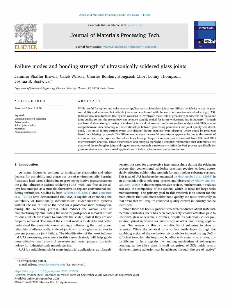
These experiments used porosity at the solder/substrate interface (termed “interfacial visual porosity”) as the quantification metric and proxy for adhesion quality and strength. The custom automated ultrasonic-assisted soldering system as described in (Shaffer et al., 2019) was used to fabricate the solder lines used in this study. To calculate the interfacial visual porosity for a solder joint, 5 equidistant 8 M P micro-scope images were taken from each side of the joint along the length of the soldered area at 50x magnification using a high-resolution camera (ProgRes Gryphax Arktur, Jenoptik). At this magnification, it is possible to detect submicron pores. The microscope images are processed using a MATLAB program described in (Maassen et al., 2020). An example of various levels of porosity is shown in Fig. 1. Here lower porosity cor-responds to an increased contact area. Note the presence of a large pore size distribution for the largest porosity (40.3 %) shown in Fig. 1, which may be caused from coalescence of microbubbles on the solder/sub-strate interface (i.e. coarsening). This is in stark contrast to the lowest porosity image (6.0 %) which shows a small range of small pores, which maximizes the solder/substrate contact area, leading to an enhanced mechanical bond.
Fig. 1. Example micrographs showing various levels of porosity and pore distributions along the solder-glass interface. The interface was observed through the underside of the glass.
J. Shaffer Brown et al.
Journal of Materials Processing Tech. 299 (2022) 117385
4
This approach is similar to the methods used by (Yih-Fong et al., 2015), wherein the intermetallic coverage was measured, as the per-centage contact of gold intermetallic phases of a ball grid array with an aluminum alloy substrate correlated heavily to the mechanical robust-ness of the joint. As Bi-Sn solders have two primary weaknesses compared to other tin-based lead-free solders – low thermal and elec-trical conductivity and brittleness (Demir et al., 2014) – a higher contact area between the solder and the glass substrate should improve the ability of the final joint to conduct more heat and increase strength. Thus, the initial working assumption was that the contact area should be directly proportional to the adhesive strength of the soldered joint. These experiments sought to correlate the interfacial visual porosity directly with the shear strength of a soldered lap shear joint. In many solar energy applications, achieving a reliable hermetic seal between components is essential to success, and Arya et al. (2021) have demonstrated the feasibility of using ultrasonic-assisted soldering with an active solder to hermetically join tempered glass panes. Studying the interfacial porosity is important, as a high level of porosity could affect the sealing qualities of the joint and provide a higher number of possible nucleation sites for cracks to form. Each of these properties of the solder joint can be critical depending on the application and location of the solder joint.
2.2. Shear strength
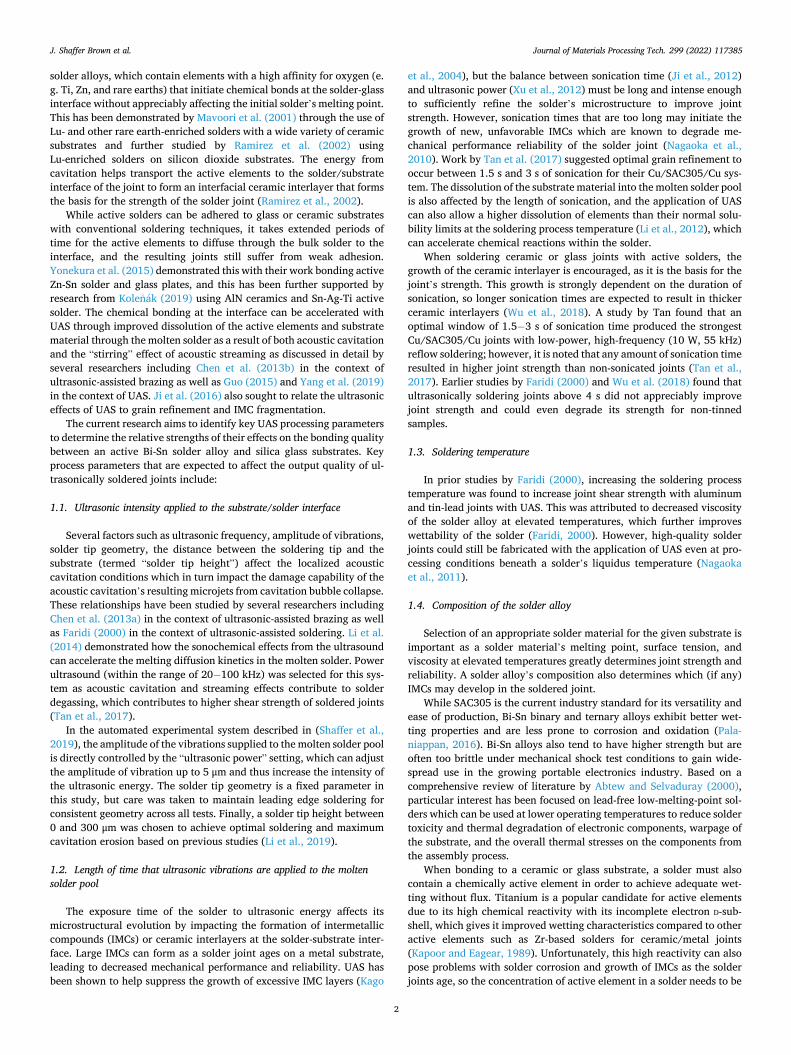
In these experiments, the goal was to better understand the corre-lation between soldering tip speeds, the resulting interfacial visual porosity, and the shear strength of the solder joint with glass substrates. An earlier design of experiments (Appendix A) suggested that the dominant factor influencing the interfacial visual porosity was the sol-dering tip speed, so only this parameter was varied in the fabrication of the shear test experimental joints while all other factors were held constant: solder tip height (0.2 mm), solder extrusion rate (0.2 mm2/ min), ultrasonic power (4.5 W). Single lap shear joints were fabricated using soldering tip speeds ranging from 10 mm/min to 1000 mm/min with a supplied power of 4.5 W and then compressively tested in shear using a custom jig, as shown in Fig. 2. A control group of non-sonicated joints soldered at a speed of 180 mm/min with the same constant pa-rameters were also tested for comparison of shear strength and porosity. The single lap shear joints (Fig. 2) were fabricated by soldering a single line of the active Bi-Sn alloy on each of the two heated cleaned silica glass microscope slides and then compressing the two together while still molten. The solder joint is then compressed with a fixed weight as the joint solidifies.
After sample fabrication, both the micro-level interfacial visual porosity and macro-level contact area between the solder and the glass
were recorded for each lap shear sample before being destructively tested for shear strength. Images were taken from both sides of the single lap shear samples to get a more representative sampling. For the macro- level contact area measurement, an additional image processing code was written to calculate the macro-level area of the solder joint in order to more accurately calculate the engineering shear stress sustained by the solder during shear testing.
Once the samples were characterized, the single lap shear samples were compressively tested in shear with a Shimadzu AGS-X universal testing machine with a constant stroke speed of 0.5 mm/min. Similar to shear-testing fixtures used by Kolenak et al. (2019), a custom 3D printed jig (Fig. 2(c)) reinforced with tool steel inserts was used to hold the single lap shear samples during testing due to the fragility and tendency of the samples to shatter if misalignment occurred during the test. The jig was designed to avoid the introduction of torque during testing, which would lead to premature failure of the solder joints. For shear testing, the maximum failure loads from the compressive shear tests were divided by the macro-level contact areas of the single lap shear samples to provide the apparent maximum shear strength to failure for each sample.
2.3. Failure surfaces
After the solder joint failed during the shear test, several represen-tative failure surfaces were selected for an SEM and EDS analysis. The purpose here was to contrast the varied failure surfaces to identify common features and then analyze the elemental composition of each failure surface. A Hitachi analytical SU6600 VP FE-SEM (Hitachi High- Tech America, Inc.) was used for analysis of the samples with an accelerating voltage of 20 kV and full vacuum. Later, the composition of the bulk solder material beneath the failure surfaces were investigated using x-ray powder diffraction (XRD) techniques with a Cu-Kα radiation as the x-ray source to determine if a difference in composition existed within the bulk region of the solder that did not include the failure surfaces. These regions were exposed by using SiC-paper of decreasing grit sizes to grind away the material from the top failure surface until the entire failure surface had been removed.
3. Results & discussion
Our initial expectation was that increased porosity at the solder-glass interface would result in reduced contact area and subsequent decrease in adhesion between the solder and the glass substrate. This was ex-pected to result in a reduced maximum shear strength before joint failure. However, experimental observations of two distinct failure surface types suggest that there is another mechanism that affects the
Fig. 2. Schematic of (a) the fabrication of a single lap shear joint with (b) side view and (c) top view when solidified. These samples were placed in the jig shown in (c) to conduct shear tests.
J. Shaffer Brown et al.
Journal of Materials Processing Tech. 299 (2022) 117385
5
maximum shear strength of the ultrasonically soldered joints. While previous studies have rarely investigated oxidation as a potential miti-gating factor when studying the strengths of ultrasonically soldered joints, visual observation of the failure surfaces suggested a more detailed analysis of the potential for accelerated oxidation of the joints under prolonged sonication by using SEM and EDS analysis.
Analysis of the pore size distribution along the soldered joint in-terfaces revealed that the majority of pores were invisible to the naked eye (less than 30 μm in diameter; area equivalent to approx. 700μm2). An average of 99.92 % of pores were invisible on the sonicated samples compared to 99.58 % for their non-sonicated counterparts. Using anal-ysis of variance (ANOVA), the percentage of visible pores among soni-cated samples was statistically different between tip speeds (p <0.0001). Of particular interest in this study were larger pores, as they represent a greater threat to solder joint performance due to their readiness to serve as nucleation sites for cracks or leakage sites for joints that need to be airtight. For the sake of comparing the frequency of large pores against tip speed, large pores were defined as those with an area exceeding 6000μm2. Using t-tests, non-sonicated samples were found to have significantly higher percentages of large pores (p = 0.0011), with large pores occurring nearly five times more often than in their soni-cated counterparts. Lastly, a statistically significant difference was found in the occurrence of large pores between tip speeds for sonicated samples (p < 0.0001) with the frequency of large pores generally increasing as solder tip speed increases.
With regards to shear testing, the inherent fragility of the lap shear samples and their sensitivity to torsional loads caused several sample joints to fail prematurely or caused the glass slides to crack or spall during testing. Despite this, a total of 88 samples were successfully tested to failure and subsequently analyzed for their maximum shear strengths before failure, with at least five successful samples for each combination of processing parameters. All samples were also analyzed for their interfacial visual porosity before shear-testing, to test for a direct correlation between maximum shear strength and interfacial vi-sual porosity. After excluding the highest and lowest result values for each parameter set, several trends began to emerge from the remaining 66 shear tests. In general, non-sonicated samples experienced the highest porosity and lowest maximum shear strength of all the samples.
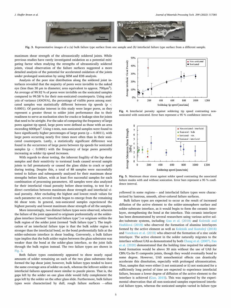
More interestingly, two distinct failure types were observed, wherein the failure of the joint appeared to originate preferentially at the solder- glass interface (termed “interfacial failure type”) or originate within the bulk region of the solder joint (termed “bulk failure type”). The impli-cation of an interfacial failure type is that the bulk solder region is stronger than the interfacial bond, so the bond preferentially fails at the solder-substrate interface in shear loading. Conversely, a bulk failure type implies that the bulk solder region between the glass substrates was weaker than the bond at the solder-glass interface, so the joint fails through the bulk region instead. The two failure types are shown in Fig. 3.
Both failure types consistently appeared to show nearly equal amounts of solder remaining on each of the two glass substrates that formed the lap shear joint; however, bulk failure types tended to leave the same coverage area of solder on each, whereas the leftover solder on interfacial failures appeared more similar to puzzle pieces. That is, the gaps left by the solder on one glass slide would fully complement the gaps left by the solder on the other glass slide. Furthermore, bulk failure types were characterized by dull, rough failure surfaces —often
yellowed in some regions— and interfacial failure types were charac-terized by lustrous, smooth, silver-colored failure surfaces.
Bulk failure types are expected to occur as the result of increased diffusion of the active element to the solder-atmosphere surface and solder-substrate interface, as it would begin to form the ceramic inter-layer, strengthening the bond at the interface. This ceramic interlayer has been demonstrated by several researchers using various active sol-der/substrate systems, including Guo et al. (2018) and Kolenak and Hodúlova (2018) who observed the formation of alumina interlayers formed by the active element as well as Kolenak and Kostolný (2018) and Yonekura et al. (2018) who observed the formation of a zinc oxide interlayer. The active element in the solder naturally migrates to the interface without UAS as demonstrated by both Chang et al. (2007). Fan et al. (2020) demonstrated that the holding time required for adequate bond formation would be above 30 min without the use of UAS for CBN/Cu-Sn-Ti composite joints, though they would eventually bond to some degree. However, UAS sonochemical effects can drastically accelerate this dissolution, especially with prolonged ultrasonication. Thus, samples that were either i) not sonicated or ii) not sonicated for a sufficiently long period of time are expected to experience interfacial failure, because a lower degree of diffusion of the active element to the interface is achieved (Guo, 2015). This was supported by the experi-mental observation that all non-sonicated samples experienced interfa-cial failure types, whereas the sonicated samples varied in failure type
Fig. 3. Representative images of a (a) bulk failure type surface from one sample and (b) interfacial failure type surface from a different sample.
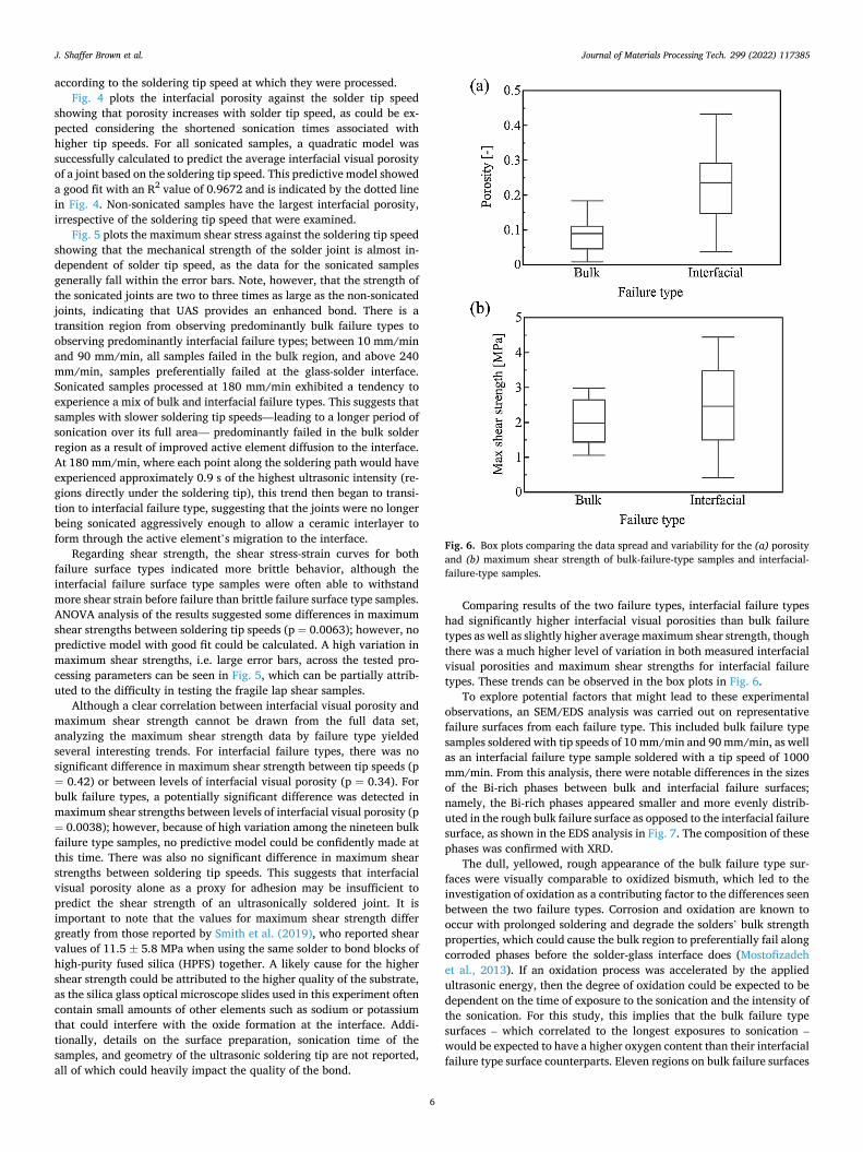
Fig. 4. Interfacial porosity against soldering tip speed contrasting non- sonicated with sonicated. Error bars represent a 95 % confidence interval.
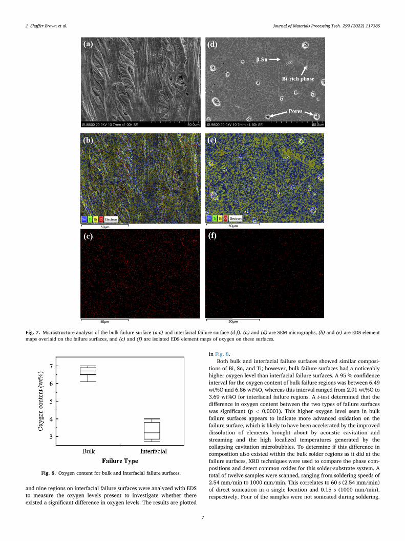
Fig. 5. Maximum shear stress against solder speed contrasting the associated failure modes with and without sonication. Error bars represent a 95 % confi-dence interval.
J. Shaffer Brown et al.
Journal of Materials Processing Tech. 299 (2022) 117385
6
according to the soldering tip speed at which they were processed. Fig. 4 plots the interfacial porosity against the solder tip speed
showing that porosity increases with solder tip speed, as could be ex-pected considering the shortened sonication times associated with higher tip speeds. For all sonicated samples, a quadratic model was successfully calculated to predict the average interfacial visual porosity of a joint based on the soldering tip speed. This predictive model showed a good fit with an R2 value of 0.9672 and is indicated by the dotted line in Fig. 4. Non-sonicated samples have the largest interfacial porosity, irrespective of the soldering tip speed that were examined.
Fig. 5 plots the maximum shear stress against the soldering tip speed showing that the mechanical strength of the solder joint is almost in-dependent of solder tip speed, as the data for the sonicated samples generally fall within the error bars. Note, however, that the strength of the sonicated joints are two to three times as large as the non-sonicated joints, indicating that UAS provides an enhanced bond. There is a transition region from observing predominantly bulk failure types to observing predominantly interfacial failure types; between 10 mm/min and 90 mm/min, all samples failed in the bulk region, and above 240 mm/min, samples preferentially failed at the glass-solder interface. Sonicated samples processed at 180 mm/min exhibited a tendency to experience a mix of bulk and interfacial failure types. This suggests that samples with slower soldering tip speeds—leading to a longer period of sonication over its full area— predominantly failed in the bulk solder region as a result of improved active element diffusion to the interface. At 180 mm/min, where each point along the soldering path would have experienced approximately 0.9 s of the highest ultrasonic intensity (re-gions directly under the soldering tip), this trend then began to transi-tion to interfacial failure type, suggesting that the joints were no longer being sonicated aggressively enough to allow a ceramic interlayer to form through the active element’s migration to the interface.
Regarding shear strength, the shear stress-strain curves for both failure surface types indicated more brittle behavior, although the interfacial failure surface type samples were often able to withstand more shear strain before failure than brittle failure surface type samples. ANOVA analysis of the results suggested some differences in maximum shear strengths between soldering tip speeds (p = 0.0063); however, no predictive model with good fit could be calculated. A high variation in maximum shear strengths, i.e. large error bars, across the tested pro-cessing parameters can be seen in Fig. 5, which can be partially attrib-uted to the difficulty in testing the fragile lap shear samples.
Although a clear correlation between interfacial visual porosity and maximum shear strength cannot be drawn from the full data set, analyzing the maximum shear strength data by failure type yielded several interesting trends. For interfacial failure types, there was no significant difference in maximum shear strength between tip speeds (p = 0.42) or between levels of interfacial visual porosity (p = 0.34). For bulk failure types, a potentially significant difference was detected in maximum shear strengths between levels of interfacial visual porosity (p = 0.0038); however, because of high variation among the nineteen bulk failure type samples, no predictive model could be confidently made at this time. There was also no significant difference in maximum shear strengths between soldering tip speeds. This suggests that interfacial visual porosity alone as a proxy for adhesion may be insufficient to predict the shear strength of an ultrasonically soldered joint. It is important to note that the values for maximum shear strength differ greatly from those reported by Smith et al. (2019), who reported shear values of 11.5 ± 5.8 MPa when using the same solder to bond blocks of high-purity fused silica (HPFS) together. A likely cause for the higher shear strength could be attributed to the higher quality of the substrate, as the silica glass optical microscope slides used in this experiment often contain small amounts of other elements such as sodium or potassium that could interfere with the oxide formation at the interface. Addi-tionally, details on the surface preparation, sonication time of the samples, and geometry of the ultrasonic soldering tip are not reported, all of which could heavily impact the quality of the bond.
Comparing results of the two failure types, interfacial failure types had significantly higher interfacial visual porosities than bulk failure types as well as slightly higher average maximum shear strength, though there was a much higher level of variation in both measured interfacial visual porosities and maximum shear strengths for interfacial failure types. These trends can be observed in the box plots in Fig. 6.
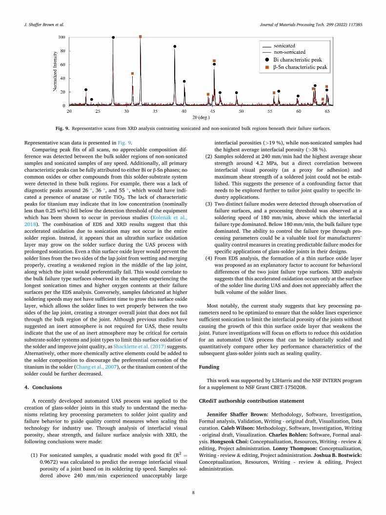
To explore potential factors that might lead to these experimental observations, an SEM/EDS analysis was carried out on representative failure surfaces from each failure type. This included bulk failure type samples soldered with tip speeds of 10 mm/min and 90 mm/min, as well as an interfacial failure type sample soldered with a tip speed of 1000 mm/min. From this analysis, there were notable differences in the sizes of the Bi-rich phases between bulk and interfacial failure surfaces; namely, the Bi-rich phases appeared smaller and more evenly distrib-uted in the rough bulk failure surface as opposed to the interfacial failure surface, as shown in the EDS analysis in Fig. 7. The composition of these phases was confirmed with XRD.
The dull, yellowed, rough appearance of the bulk failure type sur-faces were visually comparable to oxidized bismuth, which led to the investigation of oxidation as a contributing factor to the differences seen between the two failure types. Corrosion and oxidation are known to occur with prolonged soldering and degrade the solders’ bulk strength properties, which could cause the bulk region to preferentially fail along corroded phases before the solder-glass interface does (Mostofizadeh et al., 2013). If an oxidation process was accelerated by the applied ultrasonic energy, then the degree of oxidation could be expected to be dependent on the time of exposure to the sonication and the intensity of the sonication. For this study, this implies that the bulk failure type surfaces – which correlated to the longest exposures to sonication – would be expected to have a higher oxygen content than their interfacial failure type surface counterparts. Eleven regions on bulk failure surfaces
Fig. 6. Box plots comparing the data spread and variability for the (a) porosity and (b) maximum shear strength of bulk-failure-type samples and interfacial- failure-type samples.
J. Shaffer Brown et al.
Journal of Materials Processing Tech. 299 (2022) 117385
7
and nine regions on interfacial failure surfaces were analyzed with EDS to measure the oxygen levels present to investigate whether there existed a significant difference in oxygen levels. The results are plotted
in Fig. 8. Both bulk and interfacial failure surfaces showed similar composi-
tions of Bi, Sn, and Ti; however, bulk failure surfaces had a noticeably higher oxygen level than interfacial failure surfaces. A 95 % confidence interval for the oxygen content of bulk failure regions was between 6.49 wt%O and 6.86 wt%O, whereas this interval ranged from 2.91 wt%O to 3.69 wt%O for interfacial failure regions. A t-test determined that the difference in oxygen content between the two types of failure surfaces was significant (p < 0.0001). This higher oxygen level seen in bulk failure surfaces appears to indicate more advanced oxidation on the failure surface, which is likely to have been accelerated by the improved dissolution of elements brought about by acoustic cavitation and streaming and the high localized temperatures generated by the collapsing cavitation microbubbles. To determine if this difference in composition also existed within the bulk solder regions as it did at the failure surfaces, XRD techniques were used to compare the phase com-positions and detect common oxides for this solder-substrate system. A total of twelve samples were scanned, ranging from soldering speeds of 2.54 mm/min to 1000 mm/min. This correlates to 60 s (2.54 mm/min) of direct sonication in a single location and 0.15 s (1000 mm/min), respectively. Four of the samples were not sonicated during soldering.
Fig. 7. Microstructure analysis of the bulk failure surface (a-c) and interfacial failure surface (d-f). (a) and (d) are SEM micrographs, (b) and (e) are EDS element maps overlaid on the failure surfaces, and (c) and (f) are isolated EDS element maps of oxygen on these surfaces.
Fig. 8. Oxygen content for bulk and interfacial failure surfaces.
J. Shaffer Brown et al.
Journal of Materials Processing Tech. 299 (2022) 117385
8
Representative scan data is presented in Fig. 9. Comparing peak fits of all scans, no appreciable composition dif-
ference was detected between the bulk solder regions of non-sonicated samples and sonicated samples of any speed. Additionally, all primary characteristic peaks can be fully attributed to either Bi or β-Sn phases; no common oxides or other compounds from this solder-substrate system were detected in these bulk regions. For example, there was a lack of diagnostic peaks around 26 ◦, 36 ◦, and 55 ◦, which would have indi-cated a presence of anatase or rutile TiO2. The lack of characteristic peaks for titanium may indicate that its low concentration (nominally less than 0.25 wt%) fell below the detection threshold of the equipment which has been shown to occur in previous studies (Kolenak et al., 2018). The combination of EDS and XRD results suggest that this accelerated oxidation due to sonication may not occur in the entire solder region. Instead, it appears that an ultrathin surface oxidation layer may grow on the solder surface during the UAS process with prolonged sonication. Even a thin surface oxide layer would prevent the solder lines from the two sides of the lap joint from wetting and merging properly, creating a weakened region in the middle of the lap joint, along which the joint would preferentially fail. This would correlate to the bulk failure type surfaces observed in the samples experiencing the longest sonication times and higher oxygen contents at their failure surfaces per the EDS analysis. Conversely, samples fabricated at higher soldering speeds may not have sufficient time to grow this surface oxide layer, which allows the solder lines to wet properly between the two sides of the lap joint, creating a stronger overall joint that does not fail through the bulk region of the joint. Although previous studies have suggested an inert atmosphere is not required for UAS, these results indicate that the use of an inert atmosphere may be critical for certain substrate-solder systems and joint types to limit this surface oxidation of the solder and improve joint quality, as Shacklette et al. (2017) suggests. Alternatively, other more chemically active elements could be added to the solder composition to discourage the preferential corrosion of the titanium in the solder (Chang et al., 2007), or the titanium content of the solder could be further decreased.
4. Conclusions
A recently developed automated UAS process was applied to the creation of glass-solder joints in this study to understand the mecha-nisms relating key processing parameters to solder joint quality and failure behavior to guide quality control measures when scaling this technology for industry use. Through analysis of interfacial visual porosity, shear strength, and failure surface analysis with XRD, the following conclusions were made:
(1) For sonicated samples, a quadratic model with good fit (R2 =
0.9672) was calculated to predict the average interfacial visual porosity of a joint based on its soldering tip speed. Samples sol-dered above 240 mm/min experienced unacceptably large
interfacial porosities (>19 %), while non-sonicated samples had the highest average interfacial porosity (>38 %).
(2) Samples soldered at 240 mm/min had the highest average shear strength around 4.2 MPa, but a direct correlation between interfacial visual porosity (as a proxy for adhesion) and maximum shear strength of a soldered joint could not be estab-lished. This suggests the presence of a confounding factor that needs to be explored further to tailor joint quality to specific in-dustry applications.
(3) Two distinct failure modes were detected through observation of failure surfaces, and a processing threshold was observed at a soldering speed of 180 mm/min, above which the interfacial failure type dominated. Below 180 mm/min, the bulk failure type dominated. The ability to control the failure type through pro-cessing parameters could be a valuable tool for manufacturers’ quality control measures in creating predictable failure modes for specific applications of glass-solder joints in their designs.
(4) From EDS analysis, the formation of a thin surface oxide layer was proposed as an explanatory factor to account for behavioral differences of the two joint failure type surfaces. XRD analysis suggests that this accelerated oxidation occurs only at the surface of the solder line during UAS and does not appreciably affect the bulk volume of the solder lines.
Most notably, the current study suggests that key processing pa-rameters need to be optimized to ensure that the solder lines experience sufficient sonication to limit the interfacial porosity of the joints without causing the growth of this thin surface oxide layer that weakens the joint. Future investigations will focus on efforts to reduce this oxidation for an automated UAS process that can be industrially scaled and quantitatively compare other key performance characteristics of the subsequent glass-solder joints such as sealing quality.
Funding
This work was supported by L3Harris and the NSF INTERN program for a supplement to NSF Grant CBET-1750208.
CRediT authorship contribution statement
Jennifer Shaffer Brown: Methodology, Software, Investigation, Formal analysis, Validation, Writing - original draft, Visualization, Data curation. Caleb Wilson: Methodology, Software, Investigation, Writing - original draft, Visualization. Charles Bohlen: Software, Formal anal-ysis. Hongseok Choi: Conceptualization, Resources, Writing - review & editing, Project administration. Lonny Thompson: Conceptualization, Writing - review & editing, Project administration. Joshua B. Bostwick: Conceptualization, Resources, Writing - review & editing, Project administration.
Fig. 9. Representative scans from XRD analysis contrasting sonicated and non-sonicated bulk regions beneath their failure surfaces.
J. Shaffer Brown et al.
Journal of Materials Processing Tech. 299 (2022) 117385
9
Declaration of Competing Interest
The authors declare the following financial interests/personal re-lationships which may be considered as potential competing interests:
Joshua Bostwick reports financial support was provided by National Science Foundation.
Appendix A
A large-scale fractional factorial design of experiments (DOE) setup was conducted in earlier experiments following guidelines described by Antony (2014) and the microscopy protocol described in Section II with interfacial visual porosity as the quantification metric. Tested parame-ters (X1-4) and their levels are provided in Appendix Table A1. Only first and second order interactions were considered.
Results from the DOE setup are summarized in Appendix Table A2, using statistical methods described in (Ott and Longnecker, 2010) for a 95 % confidence threshold. Combined with a Pareto analysis, soldering iron tip speed was determined to be the most influential factor on determining interfacial visual porosity of the soldered joints.
References
Abtew, M., Selvaduray, G., 2000. Lead-free solders in microelectronics. Mater. Sci. Eng. R Rep. 27, 95–141.
Antony, J., 2014. Design of Experiments for Engineers and Scientists, 2nd ed. Elsevier. Arya, F., Hyde, T., Henshall, P., Eames, P., Moss, R., Shire, S., Uhomoibhi, J., 2021.
Fabrication analysis of flat vacuum enclosures for solar collectors sealed with Cerasolzer 217. Sol. Energy 220, 635–649. https://doi.org/10.1016/j. solener.2021.02.040.
Chang, S.Y., Chuang, T.H., Yang, C.L., 2007. Low temperature bonding of alumina/ alumina and alumina/copper in air using Sn3.5Ag4Ti(Ce,Ga) filler. J. Electron. Mater. 36, 1193–1198. https://doi.org/10.1007/s11664-007-0190-9.
Chen, X., Yan, J., Gao, F., Wei, J., Xu, Z., Fan, G., 2013a. Interaction behaviors at the interface between liquid Al-Si and solid Ti-6Al-4V in ultrasonic-assisted brazing in air. Ultrason. Sonochem. 20, 144–154. https://doi.org/10.1016/j. ultsonch.2012.06.011.
Chen, X., Yan, J., Ren, S., Wei, J., Wang, Q., 2013b. Microstructure and mechanical properties of Ti-6Al-4V/Al1060 joints by ultrasonic-assisted brazing in air. Mater. Lett. 95, 197–200. https://doi.org/10.1016/j.matlet.2012.12.105.
Demir, M., Aksoz, S., Oztürk, E., Maraslı, N., 2014. The measurement of thermal conductivity variation with temperature for Sn-based lead-free binary solders. Metall. Mater. Trans. B Process Metall. Mater. Process. Sci. 45, 1739–1749. https:// doi.org/10.1007/s11663-014-0109-9.
Dusek, K., Placek, M., Cepek, M., Molhanec, M., Beshajova Pelikanova, I., 2017. Ultrasonic soldering, mechanical properties of solder joints. Proceedings of the 40th International Spring Seminar on Electronics Technology. https://doi.org/10.1109/ ISSE.2017.8000925.
Fan, Y., Fan, J., Wang, C., 2020. Influence of holding time on interfacial reaction layer characteristics and wear properties of CBN/Cu-Sn-Ti composites. Metall. Mater.
Trans. B Process Metall. Mater. Process. Sci. 51, 880–884. https://doi.org/10.1007/ s11663-020-01813-z.
Faridi, H.R., 2000. Flux-free Ultrasonic Soldering of Aluminum and Stainless Steel. Oregan Graduate Institute of Science and Technology. https://doi.org/10.6083/ M44T6GNX.
Guo, W.B., 2015. Ultrasonic soldering aluminum at low temperature. Weld. J. 94, 189s–195s.
Guo, W., Luan, T., He, J., Yan, J., 2018. Ultrasonic-assisted soldering of fine-grained 7034 aluminum alloy using Sn-Zn solders below 300 ◦C. Ultrason. Sonochem. 40, 815–821. https://doi.org/10.1016/j.ultsonch.2017.08.020.
Hashemabad, S.G., Gu, Z., Ando, T., 2016. Flux-less direct soldering of aluminum by ultrasonic surface activation. J. Mater. Process. Technol. 233, 135–141. https://doi. org/10.1016/j.jmatprotec.2016.02.015.
Ji, H., Wang, Q., Li, M., 2012. Effects of ultrasonic vibration on undercooling and microstructures of SAC305 alloy. In: ICEPT-HDP 2012 Proceedings - 2012 13th International Conference on Electronic Packaging Technology and High Density Packaging. IEEE, pp. 285–288. https://doi.org/10.1109/ICEPT-HDP.2012.6474619.
Ji, H., Wang, Q., Li, M., 2016. Microstructural evolution of lead-free solder joints in ultrasonic-assisted soldering. J. Electron. Mater. 45, 88–97. https://doi.org/ 10.1007/s11664-015-4108-7.
Kago, K., Suetsugu, K., Hibino, S., Ikari, T., Furusawa, A., Takano, H., Horiuchi, T., Ishida, K., Sakaguchi, T., Kikuchi, S., Matsushige, K., 2004. Novel ultrasonic soldering technique for lead-free solders. Mater. Trans. 45, 703–709. https://doi. org/10.2320/matertrans.45.703.
Kapoor, R.R., Eagear, T.W., 1989. Tin-based reactive solders for ceramic/metal joints. Metall. Mater. Trans. B 20, 919–924. https://doi.org/10.1007/BF02670197.
Kolenak, R., 2019. Research on soldering AlN ceramics with Cu substrate using Sn-Ag-Ti solder. Solder. Surf. Mt. Technol. 31, 93–101. https://doi.org/10.1108/SSMT-10- 2018-0039.
Kolenak, R., Hodúlova, E., 2018. Study of direct soldering of Al2O3 ceramics and Cu substrate by use of Bi11Ag2La solder. Weld. World 62, 415–426. https://doi.org/ 10.1007/s40194-017-0538-6.
Kolenak, R., Kostolný, I., 2018. Investigation of flux-less soldering of metal matrix composite and ceramics by use of Zn solder. Key Eng. Mater. 759, 29–34. https:// doi.org/10.4028/www.scientific.net/KEM.759.29.
Kolenak, R., Kostolný, I., Drapala, J., Sahul, M., Urminský, J., 2018. Characterizing the soldering alloy type In–Ag–Ti and the study of direct soldering of SiC ceramics and copper. Metals (Basel) 8. https://doi.org/10.3390/met8040274.
Kolenak, R., Kostolný, I., Drapala, J., Drienovský, M., Sahul, M., 2019. Research on joining metal-ceramics composite Al/Al 2 O 3 with Cu substrate using solder type Zn–In–Mg. J. Compos. Mater. 53, 1411–1422. https://doi.org/10.1177/ 0021998319835304.
Li, Y., Leng, X., Cheng, S., Yan, J., 2012. Microstructure design and dissolution behavior between 2024 Al/Sn with the ultrasonic-associated soldering. Mater. Des. 40, 427–432. https://doi.org/10.1016/j.matdes.2012.04.002.
Li, Z., Li, M., Xiao, Y., Wang, C., 2014. Ultrarapid formation of homogeneous Cu6Sn5 and Cu3Sn intermetallic compound joints at room temperature using ultrasonic waves. Ultrason. Sonochem. 21, 924–929. https://doi.org/10.1016/j.ultsonch.2013.09.020.
Li, Z., Xu, Z., Ma, L., Wang, S., Liu, X., Yan, J., 2019. Cavitation at filler metal/substrate interface during ultrasonic-assisted soldering. Part II: cavitation erosion effect. Ultrason. Sonochem. 50, 278–288. https://doi.org/10.1016/j.ultsonch.2018.09.027.
Maassen, K.F., Brown, J.S., Choi, H., Thompson, L.L., Bostwick, J.B., 2020. Acoustic analysis of ultrasonic assisted soldering for enhanced adhesion. Ultrasonics 101. https://doi.org/10.1016/j.ultras.2019.106003.
Mavoori, H., Ramirez, A.G., Jin, S., 2001. Universal solders for direct and powerful bonding on semiconductors, diamond, and optical materials. Appl. Phys. Lett. 78, 2976–2978. https://doi.org/10.1063/1.1370985.
Mostofizadeh, M., Pippola, J., Marttila, T., Frisk, L.K., 2013. Effect of thermal aging and salt spray testing on reliability and mechanical strength of sn-58bi lead-free solder. IEEE Trans. Components Packag. Manuf. Technol. 3, 1778–1785. https://doi.org/ 10.1109/TCPMT.2013.2267333.
Nagaoka, T., Morisada, Y., Fukusumi, M., Takemoto, T., 2010. Ultrasonic-assisted soldering of 5056 aluminum alloy using quasi-melting Zn-Sn alloy. Metall. Mater. Trans. B 41B, 864–871. https://doi.org/10.1007/s11663-010-9375-3.
Nagaoka, T., Morisada, Y., Fukusumi, M., Takemoto, T., 2011. Selection of soldering temperature for ultrasonic-assisted soldering of 5056 aluminum alloy using Zn-Al system solders. J. Mater. Process. Technol. 211, 1534–1539. https://doi.org/ 10.1016/j.jmatprotec.2011.04.004.
Osorio, W.R., Peixoto, L.C., Garcia, L.R., Mangelinck-Noel, N., Garcia, A., 2013. Microstructure and mechanical properties of Sn–Bi, Sn–Ag and Sn–Zn lead-free solder alloys. J. Alloys Compd. 572, 97–106. https://doi.org/10.1016/j. jallcom.2013.03.234.
Ott, R.L., Longnecker, M., 2010. An Introduction to Statistical Methods and Data Analysis, 6th ed. Books/Cole.
Palaniappan, S.C.K., 2016. A Study on Process, Strength and Microstructure Analysis of Low Temperature SnBi-Containing Solder Pastes Mixed with Lead-free Solder Balls. Rochester Institute of Technology.
Qu, W., Zhou, S., Zhuang, H., 2015. Effect of Ti content and Y additions on oxidation behavior of SnAgTi solder and its application on dissimilar metals soldering. Mater. Des. 88, 737–742. https://doi.org/10.1016/j.matdes.2015.09.097.
Ramirez, A.G., Mavoori, H., Jin, S., 2002. Bonding nature of rare-earth-containing lead- free solders. Appl. Phys. Lett. 80, 398–400. https://doi.org/10.1063/1.1435075.
Shacklette, L.W., Gerrity, D.L., Lange, M.R., Beachboard, J.C., Smith, R., 2017. Interfacial studies of a metallurgical bond between “activated” ultrasonically applied solder and high purity fused silica. Proc. SPIE 10372, Material Technologies and Applications to
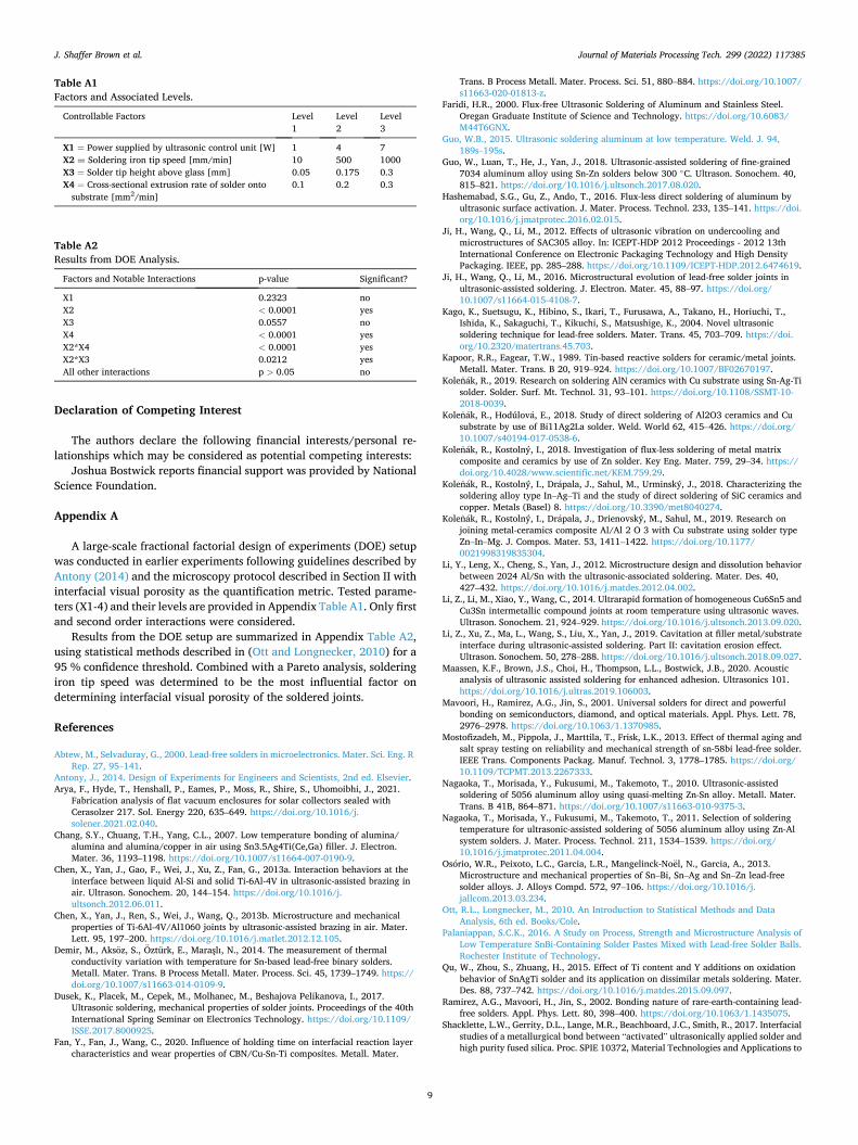
Table A1 Factors and Associated Levels.
Controllable Factors Level 1
Level 2
Level 3
X1 = Power supplied by ultrasonic control unit [W] 1 4 7 X2 ¼ Soldering iron tip speed [mm/min] 10 500 1000 X3 = Solder tip height above glass [mm] 0.05 0.175 0.3 X4 = Cross-sectional extrusion rate of solder onto
substrate [mm2/min] 0.1 0.2 0.3
Table A2 Results from DOE Analysis.
Factors and Notable Interactions p-value Significant?
X1 0.2323 no X2 < 0.0001 yes X3 0.0557 no X4 < 0.0001 yes X2*X4 < 0.0001 yes X2*X3 0.0212 yes All other interactions p > 0.05 no
J. Shaffer Brown et al.
Journal of Materials Processing Tech. 299 (2022) 117385
10
Optics, Structures, Components, and Sub-Systems III 6. https://doi.org/10.1117/ 12.2271722.
Shaffer, J., Maassen, K., Wilson, C., Tilton, P., Thompson, L., Choi, H., Bostwick, J., 2019. Development of an open-sourced automated ultrasonic-assisted soldering system. J. Manuf. Process. 47, 284–290. https://doi.org/10.1016/j.jmapro.2019.09.007.
Smith, R., Shacklette, L.W., Lange, M.R., Beachboard, J.C., Gerrity, D., 2019. S-bond active soldering of high purity fused silica for optical devices [WWW document]. S- Bond Technol. Blog. https://www.s-bond.com/blog/2019/06/10/s-bond-active-sol dering-of-high-purity-fused-silica-for-optical-devices/.
Tan, A.T., Tan, A.W., Yusof, F., 2017. Effect of ultrasonic vibration time on the Cu/Sn-Ag- Cu/Cu joint soldered by low-power-high-frequency ultrasonic-assisted reflow soldering. Ultrason. Sonochem. 34, 616–625. https://doi.org/10.1016/j. ultsonch.2016.06.039.
Wilson, C., Thompson, L., Choi, H., Bostwick, J.B., 2021. Enhanced wettability in ultrasonic-assisted soldering to glass substrates. J. Manuf. Process. 64, 276–284.
Wu, B., Guo, W., He, J., Xiu, Z., Yan, J., 2018. Microstructure evolution of SiC/SiC joints during ultrasonic-assisted air bonding using a Sn–Zn–Al alloy. Ceram. Int. 44, 1284–1290. https://doi.org/10.1016/j.ceramint.2017.07.169.
Xu, Z., Ma, L., Yan, J., Yang, S., Du, S., 2012. Wetting and oxidation during ultrasonic soldering of an alumina reinforced aluminum-copper-magnesium (2024 Al) matrix composite. Compos. Part A Appl. Sci. Manuf. 43, 407–414. https://doi.org/10.1016/ j.compositesa.2011.12.006.
Yang, H., Tan, Q., Ji, H., Wang, Z., Xu, W., Li, M., 2019. Dissolution and nucleation behavior of Al in Ta/Sn/Al joints during ultrasonic-assisted soldering. Mater. Lett. 252, 103–105. https://doi.org/10.1016/j.matlet.2019.05.103.
Yih-Fong, T., Fu-Chen, C., Chih-Huang, C., 2015. Multiple quality characteristics optimization of ball grid array wire bonding process. J. Electron. Packag. Trans. ASME 137, 1–8. https://doi.org/10.1115/1.4031471.
Yonekura, D., Ueki, T., Tokiyasu, K., Kira, S., Wakabayashi, T., 2015. Bonding mechanism of lead-free solder and glass plate by ultrasonic assisted soldering method. Mater. Des. 65, 907–913. https://doi.org/10.1016/j.matdes.2014.10.024.
Yonekura, D., Ueki, T., Taguchi, Y., 2018. Application of ultrasonic assisted soldering method to hard-to-solder material. Int. J. Mod. Phys. B 32. https://doi.org/10.1142/ S0217979218400544.
J. Shaffer Brown et al.