fabrication of an atom chip for rydberg atom-metal surface
TRANSCRIPT
Fabrication of an Atom Chip for Rydberg Atom-Metal SurfaceInteraction Studies
by
Owen Cherry
A thesispresented to the University of Waterloo
in fulfilment of thethesis requirement for the degree of
Master of Sciencein
Physics
Waterloo, Ontario, Canada, 2007c° Owen Cherry 2007

I hereby declare that I am the sole author of this thesis. This is a true copy of the thesis, including
any required final revisions, as accepted by my examiners.
I understand that my thesis may be made electronically available to the public.
Owen Cherry
ii
Abstract
This thesis outlines the fabrication of two atom chips for the study of interactions between 87Rb
Rydberg atoms and a Au surface. Atom chips yield tightly confined, cold samples of an atomic species
by generating magnetic fields with high gradients using microfabricated current-carrying wires. These
ground state atoms may in turn be excited to Rydberg states. The trapping wires of Chip 1 are
fabricated using thermally evaporated Cr/Au and patterned using lift-off photolithography. Chip 2
uses a Ti/Pd/Au tri-layer, instead of Cr/Au, to minimize interdiffusion. The chip has a thermally
evaporated Au surface layer for Rydberg atom-surface interactions, which is separated from the
underlying trapping wires by a planarizing polyimide dielectric. The polyimide was patterned using
reactive ion etching. Special attention was paid to the edge roughness and electrical properties of the
trapping wires, the planarization of the polyimide, and the grain structure of the Au surface.
iii

Acknowledgments
Over the course of my work, a number have people have offered invaluable help and to them I
feel a great deal of gratitude. First and foremost I would like to thank my supervisor, Dr. James D.
D. Martin, for all of his support and assistance throughout my research. His passion for his and his
students’ work has always inspired me.
I would like to acknowledge my M. Sc. examination committee, Dr. Jan Kycia and Dr. Xiaorong
Qin, for giving their time and valuable comments, and Dr. Donna Strickland for being a member of
my advisory committee.
The work in this thesis would not have been possible without the generosity and accommodation
of Dr. Raafat Mansour, director of the CIRFE facility, who allowed me to use the CIRFE clean room.
Without these facilities, much of the work in this thesis would not have been possible. I would also like
to thank the members of the CIRFE group for their assistance and guidance, specifically Bill Jolley
and Reena Al-Dahleh. Reena went out of her way on many occasions to help me with fabrication
processes, mask making and SEM imaging and I am truly grateful. Thank you to Roger Grant for
sharing some of his wisdom through many discussions, and to Siamak Fouladi for giving his help
with SEM imaging.
I owe a great deal of thanks to Czang-Ho Lee who, while completing his PhD thesis, spent many
late nights helping me with early stages of fabrication in the a-SiDIC clean room. Likewise, Zhara
Fakhraai who generously gave her time to take AFM for me. I would like to thank many people in
the department of physics, including Judy McDonnell for her timely reminders and Andy Colclough
for his outstanding guidance in the student machine shop.
I would like to thank my current and former group members Jeff, Parisa, Joe, Roger, Blair,
Mukto, Koroush, Maria, and Ashton. Thank you to Leslie Dema for carefully editing this thesis.
To my family and friends, thank you all so much for your constant support during my entire
university education. My parents, Lois and Nik, have helped me in so many ways over these past
eight years, including twelve moves! My brother and sister, Robin and Allison, have always been my
best friends.
iv

Dedication
This thesis is dedicated to my parents, Lois and Nik, for their unending love and encouragement.
I also dedicate this thesis to my grandmother, Marion Aitkin, whose excitement of learning is
truly inspiring.
v

Contents
1 Introduction 1
2 Background 4
2.1 Atom Chips . . . . . . . . . . . . . . . . . . . . . . . . . . . . . . . . . . . . . . . . . . 4
2.1.1 Magnetic Trapping . . . . . . . . . . . . . . . . . . . . . . . . . . . . . . . . . . 4
2.1.2 Miniaturization . . . . . . . . . . . . . . . . . . . . . . . . . . . . . . . . . . . . 7
2.1.3 Losses and Fragmentation . . . . . . . . . . . . . . . . . . . . . . . . . . . . . . 8
2.2 Rydberg Atoms Near Metal Surfaces . . . . . . . . . . . . . . . . . . . . . . . . . . . . 9
2.3 Thin Film Growth and Structure . . . . . . . . . . . . . . . . . . . . . . . . . . . . . . 11
2.3.1 Physical Vapour Deposition . . . . . . . . . . . . . . . . . . . . . . . . . . . . . 11
2.3.2 Interdiffusion . . . . . . . . . . . . . . . . . . . . . . . . . . . . . . . . . . . . . 12
3 Fabrication Methods, Materials and Devices 13
3.1 Spin Coating . . . . . . . . . . . . . . . . . . . . . . . . . . . . . . . . . . . . . . . . . 13
3.2 Metallization . . . . . . . . . . . . . . . . . . . . . . . . . . . . . . . . . . . . . . . . . 14
3.2.1 Evaporation . . . . . . . . . . . . . . . . . . . . . . . . . . . . . . . . . . . . . . 14
3.2.2 Sputtering . . . . . . . . . . . . . . . . . . . . . . . . . . . . . . . . . . . . . . . 16
vi

3.3 Photolithography . . . . . . . . . . . . . . . . . . . . . . . . . . . . . . . . . . . . . . . 18
3.3.1 Photoresist . . . . . . . . . . . . . . . . . . . . . . . . . . . . . . . . . . . . . . 18
3.3.2 Mask Aligner . . . . . . . . . . . . . . . . . . . . . . . . . . . . . . . . . . . . . 20
3.3.3 Patterning . . . . . . . . . . . . . . . . . . . . . . . . . . . . . . . . . . . . . . . 21
3.4 Planarization . . . . . . . . . . . . . . . . . . . . . . . . . . . . . . . . . . . . . . . . . 25
3.5 Reactive Ion Etching . . . . . . . . . . . . . . . . . . . . . . . . . . . . . . . . . . . . . 27
3.6 Wirebonding . . . . . . . . . . . . . . . . . . . . . . . . . . . . . . . . . . . . . . . . . 28
3.7 Scanning Electron Microscope . . . . . . . . . . . . . . . . . . . . . . . . . . . . . . . . 29
3.8 Atomic Force Microscope . . . . . . . . . . . . . . . . . . . . . . . . . . . . . . . . . . 31
3.9 Dektak Surface Profiler . . . . . . . . . . . . . . . . . . . . . . . . . . . . . . . . . . . 32
4 Atom Chip Design 33
4.1 Experimental Setup . . . . . . . . . . . . . . . . . . . . . . . . . . . . . . . . . . . . . 33
4.2 Trap Geometry and Layout . . . . . . . . . . . . . . . . . . . . . . . . . . . . . . . . . 35
4.3 Trapping Wires . . . . . . . . . . . . . . . . . . . . . . . . . . . . . . . . . . . . . . . . 37
4.3.1 Substrate . . . . . . . . . . . . . . . . . . . . . . . . . . . . . . . . . . . . . . . 37
4.3.2 Wire Material . . . . . . . . . . . . . . . . . . . . . . . . . . . . . . . . . . . . . 38
4.3.3 Wire Patterning Method . . . . . . . . . . . . . . . . . . . . . . . . . . . . . . . 39
4.4 Planarization . . . . . . . . . . . . . . . . . . . . . . . . . . . . . . . . . . . . . . . . . 40
4.5 Shield . . . . . . . . . . . . . . . . . . . . . . . . . . . . . . . . . . . . . . . . . . . . . 43
4.6 Summary . . . . . . . . . . . . . . . . . . . . . . . . . . . . . . . . . . . . . . . . . . . 45
vii
5 Atom Chip Fabrication 46
5.1 Substrate . . . . . . . . . . . . . . . . . . . . . . . . . . . . . . . . . . . . . . . . . . . 47
5.2 Trapping Wires . . . . . . . . . . . . . . . . . . . . . . . . . . . . . . . . . . . . . . . . 48
5.2.1 Mask . . . . . . . . . . . . . . . . . . . . . . . . . . . . . . . . . . . . . . . . . 49
5.2.2 Photoresist Patterning . . . . . . . . . . . . . . . . . . . . . . . . . . . . . . . . 49
5.2.3 Metal Deposition . . . . . . . . . . . . . . . . . . . . . . . . . . . . . . . . . . . 53
5.2.4 Lift-off . . . . . . . . . . . . . . . . . . . . . . . . . . . . . . . . . . . . . . . . . 58
5.2.5 Diffusion . . . . . . . . . . . . . . . . . . . . . . . . . . . . . . . . . . . . . . . 59
5.2.6 Electrical and Thermal Properties . . . . . . . . . . . . . . . . . . . . . . . . . 62
5.2.7 Wire Edges and Surface . . . . . . . . . . . . . . . . . . . . . . . . . . . . . . . 67
5.3 Planarization . . . . . . . . . . . . . . . . . . . . . . . . . . . . . . . . . . . . . . . . . 71
5.3.1 Spin-on Glass . . . . . . . . . . . . . . . . . . . . . . . . . . . . . . . . . . . . . 71
5.3.2 Polyimide . . . . . . . . . . . . . . . . . . . . . . . . . . . . . . . . . . . . . . . 74
5.3.3 Polyimide Patterning . . . . . . . . . . . . . . . . . . . . . . . . . . . . . . . . 78
5.3.4 Pinholes . . . . . . . . . . . . . . . . . . . . . . . . . . . . . . . . . . . . . . . . 82
5.3.5 Degree of Planarization . . . . . . . . . . . . . . . . . . . . . . . . . . . . . . . 84
5.4 Shield Layer . . . . . . . . . . . . . . . . . . . . . . . . . . . . . . . . . . . . . . . . . . 85
5.4.1 Grain Size and Roughness . . . . . . . . . . . . . . . . . . . . . . . . . . . . . . 90
5.5 Dicing, Assembly and Storage . . . . . . . . . . . . . . . . . . . . . . . . . . . . . . . . 93
5.5.1 Dicing . . . . . . . . . . . . . . . . . . . . . . . . . . . . . . . . . . . . . . . . . 94
5.5.2 Mounting . . . . . . . . . . . . . . . . . . . . . . . . . . . . . . . . . . . . . . . 95
5.5.3 Wirebonding . . . . . . . . . . . . . . . . . . . . . . . . . . . . . . . . . . . . . 95
5.5.4 Storage . . . . . . . . . . . . . . . . . . . . . . . . . . . . . . . . . . . . . . . . 96
viii

6 Summary and Outlook 97
Appendix I. Process Workflow 102
Appendix II. Fabricated Chips 104
Appendix III. Processing Errors 105
Appendix IV. List of Acronyms 112
Bibliography 114
ix

List of Tables
5.1 Average grain diameter vs. Au film thickness . . . . . . . . . . . . . . . . . . . . . . . 91
5.2 RMS roughness vs. Au film thickness . . . . . . . . . . . . . . . . . . . . . . . . . . . . 93
x

List of Figures
2.1 Trapping potential formed by a current carrying wire and bias field. . . . . . . . . . . 5
2.2 Configurations of U-wire and Z-wire traps and corresponding trapping potentials in
the z and y planes. . . . . . . . . . . . . . . . . . . . . . . . . . . . . . . . . . . . . . . 6
2.3 Trapping potentials for single wire and three wire guide. . . . . . . . . . . . . . . . . . 8
2.4 Diagram of electric field from Rydberg atom and image charges. . . . . . . . . . . . . 10
3.1 Typical spin curve plotting spun thickness vs. spin speed. . . . . . . . . . . . . . . . . 14
3.2 Geometric non-uniformity in evaporated film thickness. . . . . . . . . . . . . . . . . . 16
3.3 Diagram of a parallel plate sputtering system. . . . . . . . . . . . . . . . . . . . . . . . 17
3.4 Workflow for patterning photoresist. . . . . . . . . . . . . . . . . . . . . . . . . . . . . 18
3.5 Intensity at the surface of photoresist when exposed through a mask. . . . . . . . . . . 19
3.6 Slope profiles of positive and negative resists. . . . . . . . . . . . . . . . . . . . . . . . 19
3.7 Characteristic curve of a negative and positive photoresist. . . . . . . . . . . . . . . . . 20
3.8 Exposure profiles of negative resist. . . . . . . . . . . . . . . . . . . . . . . . . . . . . . 20
3.9 Three methods of patterning a metal wire. . . . . . . . . . . . . . . . . . . . . . . . . . 22
3.10 Metal evaporation vs. sputtering in lift-off lithography. . . . . . . . . . . . . . . . . . . 25
3.11 Profile of a planarizing material over patterned wires. . . . . . . . . . . . . . . . . . . 25
xi

3.12 Depth profile of interaction regions in SEM. . . . . . . . . . . . . . . . . . . . . . . . . 30
4.1 Submount for atom chip. . . . . . . . . . . . . . . . . . . . . . . . . . . . . . . . . . . . 34
4.2 Two trap configurations for chip wires. . . . . . . . . . . . . . . . . . . . . . . . . . . . 36
4.3 Layout of Chip 1. . . . . . . . . . . . . . . . . . . . . . . . . . . . . . . . . . . . . . . . 36
4.4 Layout of Chip 2. . . . . . . . . . . . . . . . . . . . . . . . . . . . . . . . . . . . . . . . 37
4.5 Three methods of achieving a planar surface above atom chip wires. . . . . . . . . . . 41
4.6 Planarization of a single wire vs. a gap. . . . . . . . . . . . . . . . . . . . . . . . . . . 43
4.7 Schematic cross section of Chip 2 design. . . . . . . . . . . . . . . . . . . . . . . . . . . 45
5.1 An outline of the fabrication process for Chip 2 . . . . . . . . . . . . . . . . . . . . . . 47
5.2 Spin curves for AZ 2000 nLOF series of photoresists. . . . . . . . . . . . . . . . . . . . 51
5.3 Modified Edwards evaporator. . . . . . . . . . . . . . . . . . . . . . . . . . . . . . . . . 54
5.4 Quartz crystal and holder for film thickness monitoring. . . . . . . . . . . . . . . . . . 55
5.5 SEM image of trapping wires of Chip 1. . . . . . . . . . . . . . . . . . . . . . . . . . . 59
5.6 SEM image of kinks in wires of Chip 1. . . . . . . . . . . . . . . . . . . . . . . . . . . 60
5.7 Change in resistance in centre wire after subjecting to polyimide cure cycles for Cr/Au,
Ti/Au, Cr/Pd/Au and Ti/Pd/Au metallizations. . . . . . . . . . . . . . . . . . . . . . 61
5.8 Test stage for atom chips. . . . . . . . . . . . . . . . . . . . . . . . . . . . . . . . . . . 62
5.9 Change in resistance due to fast heating for Cr/Au wires of Chip 1. . . . . . . . . . . . 64
5.10 Change in resistance due to slow heating for Cr/Au wires of Chip 1. . . . . . . . . . . 64
5.11 Change in resistance due to fast heating for Ti/Pd/Au wires of Chip 2. . . . . . . . . 65
5.12 Change in resistance due to slow heating for Ti/Pd/Au wires of Chip 2. . . . . . . . . 66
5.13 Change in resistance due to slow heating for Ti/Pd/Au centre wire of Chip 2 with
current through all wires. . . . . . . . . . . . . . . . . . . . . . . . . . . . . . . . . . . 66
xii

5.14 Change in resistance as a function of heating time for centre wire of Chip 1. . . . . . . 67
5.15 Change in resistance as a function of heating time for centre wire of Chip 2. . . . . . . 68
5.16 SEM image of a Chip 1 wire edge at 50,000 × magnification. . . . . . . . . . . . . . . 69
5.17 SEM image of a Chip 2 wire edge at 50,000 × magnification. . . . . . . . . . . . . . . 69
5.18 SEM image of a Chip 2 wire edge at 10,000 × magnification. . . . . . . . . . . . . . . 70
5.19 AFM image of surface of a Chip 2 wire. . . . . . . . . . . . . . . . . . . . . . . . . . . 70
5.20 Patterning of polyimide planarization layer. . . . . . . . . . . . . . . . . . . . . . . . . 72
5.21 Planarization with a single layer of T-512B spin-on glass. . . . . . . . . . . . . . . . . 73
5.22 Application process for PI 2562 and PI 2611. . . . . . . . . . . . . . . . . . . . . . . . 75
5.23 SEM image of edge of polyimide planarization layer with Al etch mask. . . . . . . . . 82
5.24 Process for eliminating holes etched through polyimide film. . . . . . . . . . . . . . . . 83
5.25 Cross section of three layers of polyimide. . . . . . . . . . . . . . . . . . . . . . . . . . 84
5.26 SEM image showing etched-back polyimide film. . . . . . . . . . . . . . . . . . . . . . 85
5.27 SEM image showing etched-back polyimide film over centre trap wires to demonstrate
planarization. . . . . . . . . . . . . . . . . . . . . . . . . . . . . . . . . . . . . . . . . . 86
5.28 Dektak profilometer scan of polyimide surface over five centre wires. . . . . . . . . . . 86
5.29 SEM image of edge of shield and polyimide layers of Chip 2. . . . . . . . . . . . . . . . 88
5.30 Image of a fabricated Chip 2 with patterned polyimide and shield layer. . . . . . . . . 89
5.31 SEM image of silver-filled Epotek H77 epoxy used to connect shield layer to ground
pads. . . . . . . . . . . . . . . . . . . . . . . . . . . . . . . . . . . . . . . . . . . . . . . 89
5.32 SEM images of thermally deposited Au (with Cr adhesion layer) over PI 2562. . . . . 90
5.33 AFM scans of Au films on polyimide. . . . . . . . . . . . . . . . . . . . . . . . . . . . . 92
5.34 RMS roughness of thermally deposited Au on polyimide (with Cr adhesion layer) for
four thicknesses. . . . . . . . . . . . . . . . . . . . . . . . . . . . . . . . . . . . . . . . 93
xiii

5.35 SEM image of 100 nm Au layer on polyimide. . . . . . . . . . . . . . . . . . . . . . . . 94
5.36 Chip 1 mounted to Macor block. . . . . . . . . . . . . . . . . . . . . . . . . . . . . . . 96
6.1 “Reverse Fabrication” method to attain a single crystal Au shield layer. . . . . . . . . 99
6.2 Connecting a Au electrode to underlying Au using via etched through polyimide. . . . 100
6.3 Absorption image of 87Rb atoms magnetically trapped with macroscopic Z-wire and
external field coils. . . . . . . . . . . . . . . . . . . . . . . . . . . . . . . . . . . . . . . 101
xiv

Chapter 1
Introduction
A Rydberg atom has a single electron excited to a state with a high principal quantum number, n
[1]. The size of a Rydberg atom scales as n2, and likewise the electric transition dipole moment to
energetically similar states. Close to a metal surface, a Rydberg atom generates a surface charge
that arranges to mimic an image of the atom. Dipole-dipole interactions between Rydberg atoms
and their “image charges” shift and broaden the atomic energy levels through perturbations of the
Rydberg electron wavefunction [2]. Since it is highly excited, the Rydberg electron is loosely bound.
At short atom-surface distances it may be stripped from the atom through an attraction to its image
(creating an ion).
Previously, the interactions between Rydberg atoms and metal surfaces have been studied using
thermal atomic beams [3]. These collimated beams are optically excited to Rydberg states and
intersect the surface at near-grazing incidence. By measuring ion signal as a function of applied
electric field, atom-surface distance may be inferred. However, as the Rydberg atom moves towards
the surface it undergoes a complex interaction with the surface. As a result, the character of the
Rydberg wavefunction changes significantly before ionization [4]. As this wavefunction character is
thought to significantly influence the ionization event, this situation is not ideal.
Magnetic microtraps, or “atom chips”, offer an alternate method of studying Rydberg atoms
close to a surface. An atom chip uses current-carrying wires, microfabricated on a substrate, to form
1

a magnetic potential minimum above the chip’s surface [5]. Weak field-seeking atoms are attracted
to the minimum and thus contained. Control over the location of the potential minimum, and the
gradient and curvature around it, allows one to accurately manipulate the position and size of the
trapped atom cloud. Therefore, the distance between the atoms and the surface of the chip is well-
defined and controllable, in contrast to Rydberg atom-surface interaction experiments which employ
thermal beams. We plan to use an atom chip to magnetically trap 87Rb atoms and bring them close
(within μm) to the chip’s metal surface. There they will be excited to Rydberg states, and we will
study shifts and/or broadenings of the spectral lines to probe surface interactions. Although the
Rydberg atoms will not be trapped, the timescale of the interactions and spectroscopy is less than
that of the thermal expansion of the atomic cloud.
Atom chips have been used as tools for: creating Bose-Einstein condensates (BEC1); manipulating
atoms with guides; beamsplitters and “conveyor belts”; splitting and recombining clouds of atoms
for interference studies; and many other experiments with integrated atom optics [6], [7]. However,
to this date there has been little crossover between a Rydberg atom physics and atom chips2.
In this thesis, I describe in detail the fabrication of atom chips intended for the study of Rydberg
atom-metal surface interactions. Two designs of atom chips have been fabricated. Chip 1 is a simple
design, used to gain experience with magnetic trapping techniques. Chip 2 is a multi-layer design,
specialized for studying interactions between a Rydberg atom and its metal surface. This thesis is
intended as a comprehensive guide to the fabrication of the chips. Specific details of the design of the
atom chips will be found in a fellow graduate student Jeff Carter’s M.Sc. thesis [9]. His thesis will
also contain a discussion of the laser cooling and trapping scheme, preliminary magnetic trapping
and trapped atom imaging.
The thesis is divided into six chapters. Chapter 2 gives a background of magnetic trapping
and atom chips. It then offers an overview of Rydberg atoms and their interactions with metal
surfaces, including the effects of randomly distributed “patch potentials”. Growth and diffusion
mechanisms of thin films are also discussed. Chapter 3 is an overview of the relevant methods and1A list of acronyms is found in Appendix I.2An atom chip for trapping Rydberg atoms has been proposed by Mozley et. al . [8].
2

devices that are used in atom chip fabrication. This includes thin film deposition, patterning with
photolithography, and planarization. It concludes with metrology techniques (surface profilometry
and scanning electron microscopy) used to characterize microfabricated devices. Chapter 4 presents
the design of the two atom chips. The chapter begins with an overview of the experimental setup to
illustrate the role of the atom chips in the planned Rydberg atom-surface studies. The design and
fabrication method of each layer of the chips is given, supported by a summary of methods used by
other groups. Detailed methods of the fabrication of Chip 1 and Chip 2 are given in Chapter 5. In
addition, it includes measurements of important aspects of the fabricated chips, including thermal
properties, wire edge roughness, planarization and grain structure and roughness of the top surface.
The thesis concludes with a summary and a discussion of possible continuing work on this project.
3
Chapter 2
Background
2.1 Atom Chips
2.1.1 Magnetic Trapping
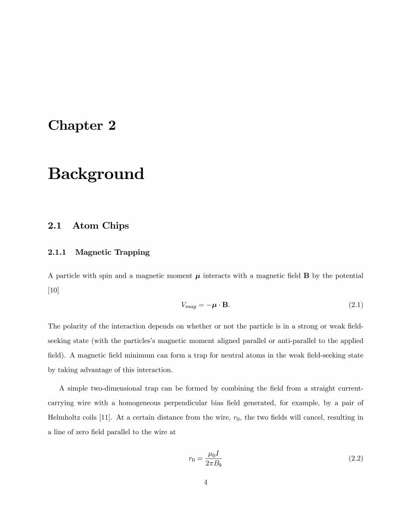
A particle with spin and a magnetic moment μ interacts with a magnetic field B by the potential
[10]
Vmag = −μ ·B. (2.1)
The polarity of the interaction depends on whether or not the particle is in a strong or weak field-
seeking state (with the particles’s magnetic moment aligned parallel or anti-parallel to the applied
field). A magnetic field minimum can form a trap for neutral atoms in the weak field-seeking state
by taking advantage of this interaction.
A simple two-dimensional trap can be formed by combining the field from a straight current-
carrying wire with a homogeneous perpendicular bias field generated, for example, by a pair of
Helmholtz coils [11]. At a certain distance from the wire, r0, the two fields will cancel, resulting in
a line of zero field parallel to the wire at
r0 =μ0I
2πBb(2.2)
4

r0
Figure 2.1: Trapping potential formed by a wire carrying current (out of page) and a homogeneousbias field (B0).
where I is the current in the wire and Bb is the magnitude of the bias field (see Figure 2.1). The
position of r0 can be controlled by varying I and Bb, allowing for precise positioning of the trapped
atoms. Near r0 the gradient of the resulting field is [6]
∇B = 2πB2bμ0I
=μ0I
2πr20. (2.3)
With a straight wire and a bias field, atoms are guided in just two dimensions, with no axial
component to the potential. By bending the ends of the wire to form a U or Z, atoms can be trapped
in all three-dimensions, with the bent sections contributing field components orthogonal to the bias
field [5] (see Figure 2.2).
When trapping atoms, a field zero is not desirable, since atoms can spin-flip into the untrapped
strong field-seeking state when passing near or through the zero. These are known as Majorana spin-
flips. For a straight wire guide, adding a homogeneous axial field raises the trap minimum to form an
Ioffe-Pritchard trap. Conventionally, this field is labelled BIP and it converts the potential around
the trap minimum from quadrupolar to harmonic. For a U-trap, the fields from the two bent ends
cancel at the trap centre and give a field-zero. A Z-trap, however, naturally forms a Ioffe-Pritchard
trap and an additional BIP can further lift the minimum. The trapping potentials of U- and Z-wire
5
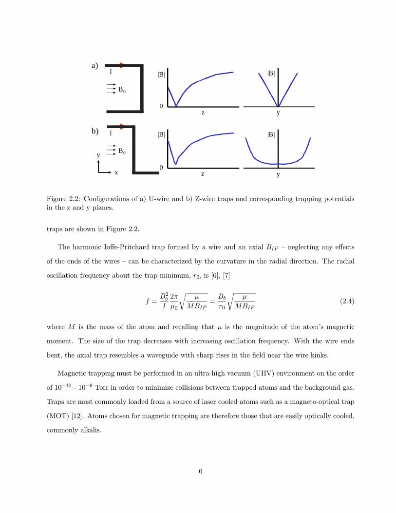
a)
b)
y
x
|B|
B0
B0
I
I
z
z
y
y
0
0
|B|
|B||B|
Figure 2.2: Configurations of a) U-wire and b) Z-wire traps and corresponding trapping potentialsin the z and y planes.
traps are shown in Figure 2.2.
The harmonic Ioffe-Pritchard trap formed by a wire and an axial BIP — neglecting any effects
of the ends of the wires — can be characterized by the curvature in the radial direction. The radial
oscillation frequency about the trap minimum, r0, is [6], [7]
f =B2bI
2π
μ0
rμ
MBIP=Bbr0
rμ
MBIP(2.4)
where M is the mass of the atom and recalling that μ is the magnitude of the atom’s magnetic
moment. The size of the trap decreases with increasing oscillation frequency. With the wire ends
bent, the axial trap resembles a waveguide with sharp rises in the field near the wire kinks.
Magnetic trapping must be performed in an ultra-high vacuum (UHV) environment on the order
of 10−10 - 10−9 Torr in order to minimize collisions between trapped atoms and the background gas.
Traps are most commonly loaded from a source of laser cooled atoms such as a magneto-optical trap
(MOT) [12]. Atoms chosen for magnetic trapping are therefore those that are easily optically cooled,
commonly alkalis.
6

2.1.2 Miniaturization
The maximum trap gradient, ∇B, for a wire with radius r0 is at a distance r0 from the wire surface.
Therefore, from Equation 2.3, ∇B ∝ j, where j is the current density in the wire [13]. The achievable
current density scales inversely with wire radius, favouring miniaturization. Fabricating the wires on
a substrate allows for extremely small wires and further increases the maximum current density by
improving heat transport, as first proposed by Weinstein et al . [10] in 1995. The first substrate-based
magnetic traps were fabricated by Drndic et al . [13] (1998), Reichel et al . [5] (1999), and Folman et
al . [14] (2000), with the latter group introducing the term “atom chip”. These chips were made using
the established metal deposition and lithography techniques used in semiconductor manufacturing
(see Section 3). A diagram of the potential formed by an atom chip wire and external bias field is
shown in Figure 2.3a.
Miniaturization allows for a high degree of accuracy in positioning trapped atoms. Complex trap
geometries with multiple wires can also be realized, giving the ability to transport, split and merge
collections of atoms1. Shortly after successes with magnetically trapping with wires on a substrate,
the first Bose-Einstein condensate (BEC) was created using an atom chip in 2001 [16], [17]. Since
then, atom chip-based experiments have expanded to include BEC interferometry and diffraction,
double-well potentials and single atom detection.
More complex traps can be formed by crossing wires. Lev [15] explains the multiple uses of a grid
of wires for forming U-, Z- and H-shaped configurations as well as “gates” for transporting atoms.
Reichel et al .[5] introduced the “atomic conveyor belt”, which uses a corrugated wire on each side of
the main guide wire to transport atoms over a distance of millimetres.
In many cases, the external coils that generate the bias field can be replaced by additional wires
on the chip to form tighter traps close to the surface (Figure 2.3b). An added advantage of this is
that the orientation of the fields is accurately fixed, simplifying the positioning of the trap. Also,
the microfabricated wires have a much lower inductance than macroscopic external coils and can
therefore be switched off and on more quickly.1Excellent reviews of atom chip design, fabrication and experiments have been written [6], [7], [15].
7

a) b)
Figure 2.3: Trapping potentials for a) single wire and external bias field, b) three wire guide.
As the applications of atom chips progress, so too does the need for advanced fabrication tech-
niques. As will be discussed throughout this thesis, the thermal properties of the substrate, roughness
of the wires, and smoothness and reflectivity of the chip surface can be extremely important in atom
chip experiments.
2.1.3 Losses and Fragmentation
Many loss mechanisms come into play when magnetically trapping atoms with chips. Atoms can be
lost from the trap due to Majorana flips, collisions with the background gas or other trapped atoms,
or tunneling and noise induced spin flips to untrapped states [6]. Another significant cause of loss is
interactions between the trapped atoms and noise in the electromagnetic field due to the vicinity of
the chip. This noise is caused by thermally induced currents in the chip surface [18] and, to some
degree, shot noise in the current carrying wires.
Random thermally-induced currents in the surface material cause fluctuations in the electromag-
netic field. These fluctuations can cause spin-flips in the trapped atoms, leading to a decrease in
trap lifetime. The loss rate is dependant on the skin depth of the material at the Larmor frequency
of the trapped atoms (δ), the thickness of the surface (d) and the atom-surface distance (y). This
8

loss rate, γ, is approximated to be [19]
γ ∝ d
δ2y2, d¿ y ¿ δ (2.5)
for thin films. Various experiments have been performed to measure trap losses due to surface
proximity using both ultracold clouds and condensates [20], [21], [22], [23].
When first cooling trapped atoms to BEC near metal surfaces, it was observed that the cloud
was not uniform and was instead fragmented into smaller clouds [20], [24], [25]. The severity of the
fragmentation was found to depend on the average distance between the cloud and the surface by
Fortágh et al . [20] and was caused by irregularities in the magnetic field [24]. The dominant cause of
roughness in the magnetic field is deviations in the current flow in the trapping wires. Roughness in
the wire edges and surface causes the current to stray from a straight path, generating a corrugated
axial component to the magnetic field [26]. Wire edge and surface roughness is a result of the
fabrication method, and it can be minimized with advanced techniques [27] (see Section 4.3.3).
2.2 Rydberg Atoms Near Metal Surfaces
The size of a Rydberg atom scales as n2, as measured by Fabre et al . [28], which causes exaggerated
behaviour. Rydberg atoms are extremely sensitive to electric fields since the excited electron is so
loosely bound. The polarizability of Rydberg atoms scales as n7 and therefore modest fields can
strongly perturb Rydberg energy levels through Stark shifts, or even ionize the atoms [1]. Therefore,
Rydberg atoms are ideal probes of small variations in electric fields [29]. Due to the separation
between the Rydberg electron and the core, the electric transition dipole moment is large and scales
with the separation.
Near a metal surface, the Rydberg electron and ion core generate a charge distribution over the
surface with an electric field that mimics that from a corresponding positive and negative image
charge embedded in the metal (Figure 2.4). The Rydberg electron is attracted by its image through
a dipole-dipole interaction, and at close enough distances the electron can be stripped from the atom
9

+
-+
-
Figure 2.4: Diagram of electric field from Rydberg electron and ion core and corresponding imagecharges.
by field ionization [28]. The distance at which ionization occurs is [30]
r = 3.8n2a0 (2.6)
where a0 is the Bohr radius.
At greater atom-surface distances, the interaction between the Rydberg atom and its image leads
to a perturbative energy level shift known as the Lennard-Jones shift [31]. At intermediate distances
the orientation of the Rydberg atom with respect to the surface becomes important [30]. States
where the electron is most often between the core and the surface (“red” states) experience greater
broadenings than states where the electron is on the opposite side of the core form the surface
(“blue” states). However, as the surface is approached a particular energy level may alternate from
red to blue and back due to state mixing and avoided crossings from surface induced perturbations.
Therefore, a high degree of control over atom-surface distance is required, which can be realized with
magnetic trapping using an atom chip.
A polycrystalline material has grains with random crystal orientations with respect to the surface.
Difference in the work function between the grains generate electric fields that may have effects on
Rydberg atoms that overshadow other atom-surface interactions. The effect of “patch fields” has
been observed in studies of gravitation [32], [33] and ion trapping [34], [35]. This effect can be
10
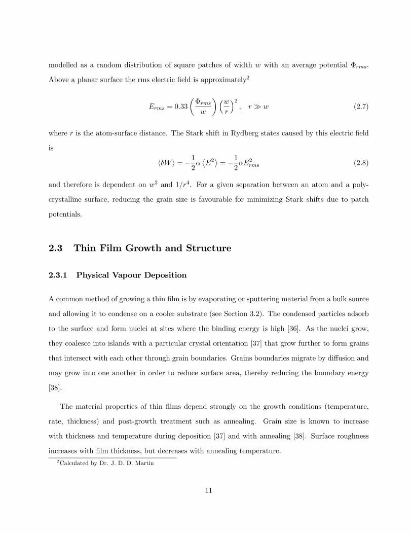
modelled as a random distribution of square patches of width w with an average potential Φrms.
Above a planar surface the rms electric field is approximately2
Erms = 0.33
µΦrmsw
¶³wr
´2, r À w (2.7)
where r is the atom-surface distance. The Stark shift in Rydberg states caused by this electric field
is
hδW i = −12αE2®= −1
2αE2rms (2.8)
and therefore is dependent on w2 and 1/r4. For a given separation between an atom and a poly-
crystalline surface, reducing the grain size is favourable for minimizing Stark shifts due to patch
potentials.
2.3 Thin Film Growth and Structure
2.3.1 Physical Vapour Deposition
A common method of growing a thin film is by evaporating or sputtering material from a bulk source
and allowing it to condense on a cooler substrate (see Section 3.2). The condensed particles adsorb
to the surface and form nuclei at sites where the binding energy is high [36]. As the nuclei grow,
they coalesce into islands with a particular crystal orientation [37] that grow further to form grains
that intersect with each other through grain boundaries. Grains boundaries migrate by diffusion and
may grow into one another in order to reduce surface area, thereby reducing the boundary energy
[38].
The material properties of thin films depend strongly on the growth conditions (temperature,
rate, thickness) and post-growth treatment such as annealing. Grain size is known to increase
with thickness and temperature during deposition [37] and with annealing [38]. Surface roughness
increases with film thickness, but decreases with annealing temperature.2Calculated by Dr. J. D. D. Martin
11

2.3.2 Interdiffusion
Highly conductive metals, such as Au, have low reactivity with other materials and often require
an intermediate layer that is reactive with both the substrate and the conductive layer. These
adhesion layers are commonly Cr and Ti, which function well as long as the films are not subjected
to subsequent high temperature processes. At elevated temperatures these films can interdiffuse,
often with considerable changes to material properties such as resistivity, adhesion, and stress [39].
In designing and fabricating metallized microelectronic devices, diffusion must be taken into account
when higher temperature processes are required. For an infinite source, the rate of diffusion is
governed by [36]
Rate ∝ expµ− QkT
¶(2.9)
where Q is the activation energy, k is Boltzmann’s constant and T is the temperature.
Diffusion processes between various adhesion layers and gold have been studied extensively by:
measuring resistivity changes in the film [40], [41]; resistivity and surface profiles at the interface
between layers [42]; surface imaging with electron microscopes and atomic force microscopes [40],
[41], [43]; and depth profiling using Rutherford backscattering [44].
Since thin films consist of grains, grain boundaries and dislocations, interdiffusion is not uniform
across the interface between two thin films. The bulk of diffusing material has been found to
preferentially travel through grain boundaries until reaching the surface [39]. This process continues
until the diffusing lower layer is depleted and the bulk of the diffusing material has accumulated at
the surface. Materials such as chromium and titanium form oxides on or near the surface [40], [43].
The use of an intermediate buffer layer between the adhesion and conducting layers is commonly
used to reduce interdiffusion and has been studied for various film combinations including Ti/Pd/Au
[44], NiCr/Pd/Au [45], and Ti/Pt/Au [46].
12

Chapter 3
Fabrication Methods, Materials and
Devices
This chapter introduces the relevant methods that are used to fabricate atom chips. It begins with
methods of coating substrates with thin films of polymers and metals through spinning, evaporating
and sputtering. Next, photolithographic patterning of these films is explained, followed by methods
of attaining planar surfaces above them. Finally, it ends with a description of devices used to
characterize topography and surface properties of microfabricated films and structures. This chapter
is intended as a general overview of the important aspects of fabrication. Specific recipes are given
in the following chapters.
3.1 Spin Coating
Spin coating is a method of applying a thin, uniform layer of material (often organic) across the
surface of a wafer. The material is usually dissolved in a solvent, with the concentration determining
the viscosity. The liquid is dispensed onto the wafer surface using a syringe, a pipette, or by pouring.
The wafer is spun between 500 and 5000 RPM and the centrifugal force causes the liquid to spread
out radially over the surface, with the excess flung from the wafer edge. The wafer is then baked to
13

ϖ
t
Figure 3.1: Typical spin curve plotting spun thickness vs. spin speed [48].
drive off the solvent and harden the film.
The thickness of the film depends on the spin speed and the viscosity of the liquid. Spun and
baked photoresist, for example, is most commonly 500 nm to 5μm. Thick film resists and materials
such as SU8 can be spun in a single layer, tens of microns thick, or much thicker with multiple layers
[47]. The dependence of the thickness of a spun material, t, to spin speed, ω, is characterized by a
spin curve, as illustrated in Figure 3.1.
3.2 Metallization
Metal films can be grown on a surface physically (vapour deposition) or chemically (electroplating,
see Section 3.3.3), depending on the requirements of the film or the fabrication process.
3.2.1 Evaporation
The simplest method of growing a metal film is by evaporating a small amount of metal, either
resistively or with an electron beam, and allowing it to deposit on the sample [36]. Keeping the
system at low pressure (< 10−5 torr) minimizes the presence of background gas, increasing the mean
free path of the metal particles and avoiding contamination of the film. Therefore, evaporated metal
does not coat the sidewalls of vertical features (low step coverage).
14

In a typical thermal evaporator, a crucible containing the source of metal (charge) is placed in a
tungsten coil which is resistively heated. The current passing through the tungsten wire determines
the crucible temperature and thus the rate of evaporation. Film deposition rate and thickness is
monitored using a quartz crystal oscillator which decreases in resonant frequency as material is built
up on its surface (Section 5.2.3).
The advantage of this system is that it is simple, and affordable to operate and maintain. There
are, however, several disadvantages. Deposition rate is highly dependant on the thermal contact
between the coil and crucible and on the surface area of the charge, making results for a given
current and time inconsistent from run to run. Additionally, radiation from the hot charge, crucible
and coil can cause unwanted heating of the substrate.
Electron beam deposition systems use a focussed beam of electrons to heat just the top surface of
the charge. Deposition rates are much more consistent than resistively-heated evaporators, since the
evaporation of the charge is controlled by the electron beam spot size and the intensity [49]. While
heating of the substrate due to thermal radiation is much less in electron-beam systems, films can
be damaged by high energy electrons from the electron gun.
It is often useful to deposit layers of more than one type of material. With a resistive evaporation
system, each charge must have a separate current source, usually powered with a switchable trans-
former. In an electron beam evaporator, a charge does not require an external electrical connection,
so each crucible can be moved into the path of the beam when needed.
With both evaporation methods the deposited film thickness is not uniform across the sample.
If the evaporating material is considered to emit from a point source, the arrival rate across the
sample decreases with cos3 θ for a given perpendicular charge-sample distance, L [50], with θ defined
in Figure 3.2. This effect limits the surface area that can be uniformly coated and thus the number
of samples that can be coated simultaneously. Simply placing the sample or samples further from
the source decreases the angle to improve uniformity, however more material is wasted to the walls
of the chamber. A solution for coating multiple wafers is to place them on a rotary or planetary
stage, offset from the source so that each wafer passes directly over the source multiple times during
15

ΥL
Figure 3.2: Geometric non-uniformity in evaporated film thickness.
the deposition [49].
3.2.2 Sputtering
An alternate method of thin film deposition is by sputtering material from a target using energetic
ions [36]. When ions bombard a surface, many interactions can occur including scattering, dislo-
cations, ion implantation, and electron emission. As well, impacting ions can cause a collisional
cascade of atoms in the material. If atoms near the surface collide with energies greater than the
surface binding energy, atoms can be ejected from the surface [50]. Sputtering systems put several
kV between two plates in a chamber with Ar or Xe gas at pressures between 10−1 and 10−2 torr in
order to form a plasma. The target, a high purity plate of the material to be sputtered, forms the
cathode and particles of the ionized gas are accelerated towards it (Figure 3.3).
For sputtering metals, a dc potential is sufficient. Insulators, however, quickly build up a surface
charge in a dc field and rf potentials are required instead.
Due to the high pressures required to form a plasma the mean free path of the sputtered particles
is quite low (∼ 1mm) [36]. Particles arrive at the substrate at a large range of angles giving a high
16

Ar in Pump
Target (Cathode)
Substrate
Anode
Plasma
+
Figure 3.3: Diagram of a parallel plate sputtering system.
degree of step coverage. Sputtering is therefore preferable to evaporation for coating over features
with topography.
Sputtering has other advantages over thermal/electron beam deposition. Sputtering systems
can be very compact with simple turn-key operation. Deposition rates are consistent from coating
to coating. Material properties of the film (grain size and structure, stress) can be consistently
controlled by varying chamber pressure, deposition rate and substrate temperature [51]. Alloys and
mixtures of two or more metals can be sputtered, with the ratio between species in the sputtered
film matching the target composition.
A disadvantage of sputtering is that deposition rates are much slower than thermal evaporation.
The bombarding ions dissipate most of their energy into the target, causing heating. The heating
sets a maximum on ion energy, which limits the sputtering rate. Another disadvantage of sputtering
is that the step coverage, while useful in some situations, is detrimental to lift-off photolithography
(Section 3.3.3). The sputtered film coats the sidewalls of the photoresist (high step coverage), making
chemical access difficult and giving rough feature edges.
17

Coat substrate with photoresist
Soft-bake
Align and expose
Post-exposure bake
Develop
Hard-bake(depending on resist)
Figure 3.4: Workflow for patterning photoresist.
3.3 Photolithography
3.3.1 Photoresist
Photolithography is the basis for nearly all microfabrication technology as the means of transferring
patterns to a substrate. A photosensitive material is exposed to a light field shone through a mask
that contains a replica of the desired pattern [48]. Typically, this material is an organic polymer,
known as “photoresist”, that is sensitive to ultraviolet radiation. It is applied to the substrate (wafer)
by dropping a small amount onto the surface and spinning at a high rate to give a uniform layer
(Section 3.1). The resist is then baked to drive off solvents and exposed for a set amount of time to
UV light shone through a mask. After exposure the resist is developed, leaving resist matching the
pattern on the mask. Figure 3.4 shows the typical process for patterning photoresist.
Photoresist can be one of two tones, ‘positive’ or ‘negative’, which differ depending on how
light influences the polymer. Positive photoresists are relatively insoluble in resist developer unless
18

Inte
nsity
a) b)
Figure 3.5: Intensity at the surface of photoresist when exposed through a mask with a) no diffractionand b) with diffraction.
a) b)
Figure 3.6: a) Positive-slope profile of positive photoresist. b) Negative-slope profile of negativephotoresist.
exposed to UV light, which breaks bonds in the polymer structure. Negative resists are soluble in
the developer chemicals until exposure promotes cross-linking between polymers.
On the scale of typical photolithography features, diffraction plays an important role, broadening
the intensity profile after edges on the mask pattern. Consequently, the surface of the photoresist
does not receive a spatially uniform dose (Figure 3.5). This effects the edge profile (sidewall) of the
resist. A positive resist exhibits a positively-sloped sidewall, since the edge of a feature is exposed
to less energy than the centre (Figure 3.6a). The same is true for negative resist, only the falloff in
dose at a feature edge results in a negatively-sloped sidewall, known as undercut (Figure 3.6b). It is
the polarity and angle of sidewall slope that determines the type of resist best suited for a particular
lithographic process.
A photoresist has two exposure thresholds, between which the resist only partially develops.
A quantitative way to characterize photoresist is by its contrast. Contrast can be determined by
19
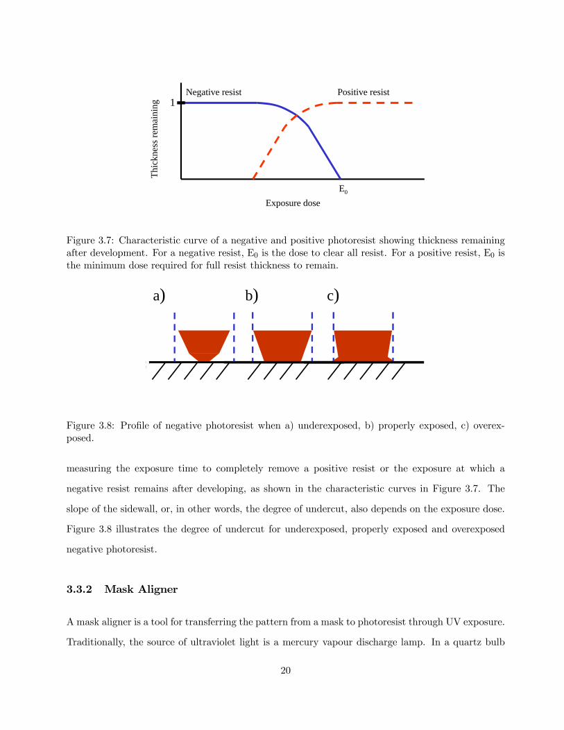
Exposure dose
Thic
knes
s rem
aini
ng
E0
Negative resist Positive resist1
Figure 3.7: Characteristic curve of a negative and positive photoresist showing thickness remainingafter development. For a negative resist, E0 is the dose to clear all resist. For a positive resist, E0 isthe minimum dose required for full resist thickness to remain.
a) b) c)
Figure 3.8: Profile of negative photoresist when a) underexposed, b) properly exposed, c) overex-posed.
measuring the exposure time to completely remove a positive resist or the exposure at which a
negative resist remains after developing, as shown in the characteristic curves in Figure 3.7. The
slope of the sidewall, or, in other words, the degree of undercut, also depends on the exposure dose.
Figure 3.8 illustrates the degree of undercut for underexposed, properly exposed and overexposed
negative photoresist.
3.3.2 Mask Aligner
A mask aligner is a tool for transferring the pattern from a mask to photoresist through UV exposure.
Traditionally, the source of ultraviolet light is a mercury vapour discharge lamp. In a quartz bulb
20

a pair of electrodes excite a vapour of mercury causing it to emit a spectrum of radiation [52].
Common photoresists are sensitive to either the 365 nm (i-line) or the 436 nm (g-line) peaks [48]. In
many aligners a filter reflects unwanted wavelengths to a heat sink and allows just the i-line or g-line
radiation to pass. The light from the mercury discharge lamp is collected by an ellipsoidal mirror
and passed to the collimation optics.
Three types of mask aligners are commonly used: contact, proximity and projection [48]. Contact
aligners place the mask and wafer in direct contact with each other in order to minimize the effects of
diffraction at the edges of mask features. The drawback is that there is a risk of damage to either the
mask or the wafer. Also, photoresist may stick to the mask, requiring frequent cleaning of the mask.
Proximity aligners leave a small gap between the mask and wafer to avoid problems arising from
contact between the two. However, diffraction limits the resolution. A simple projection printing
system places optics between the mask and the wafer to focus the ultraviolet light onto the wafer.
Currently, most industrial projection printers use reduction optics to shrink the feature size by at
least an order of magnitude, from the mask to the wafer, to achieve smaller features.
The position of the mask over the wafer is set by matching alignment marks on the mask with
those on the wafer. Two alignment marks can be imaged simultaneously using a split-field microscope.
Translation and rotation controls are used to achieve alignment.
3.3.3 Patterning
Photoresist is primarily used as a mask for transferring a pattern to a layer or layers of metal, oxide
or polymer. Resist can be applied after depositing the layer as a mask for removal, or it can be
applied before to define where the layer is grown. Figure 3.9 shows three methods of patterning a
wire on a substrate using etching, electroplating and lift-off.
Etching
The most common method of transferring a pattern from a mask to a layer of material on a wafer
is by etching [49] (Figure 3.9a). Positive photoresist is spun over the material and patterned using
21

a) b) c)
Etchant
I
Evaporant
Evaporant
Evaporant = Photoresist
Figure 3.9: Three methods of patterning a metal wire: a) etching, b) electroplating and c) lift-off.
22

a positive-image mask (i.e. opaque where the material is to remain). Positive resist is used because
the base of the resist profile matches the features on the mask so they are accurately translated to
the etched film (see Figure 3.8a). Once exposed, baked and developed the positive resist is used as
a mask to etch the underlying material through either a ‘wet’ or ‘dry’ process.
Wet etching involves immersing the wafer in a liquid etchant that is highly selective between the
material to be etched and the etch mask (for example, Au is etched in KI and SiO2 in HF). The
etchant is often heated and the wafer agitated to ensure a uniform etch with a consistent rate.
Dry etching includes reactive ion etching (Section 3.5) and ion milling. In both cases ions are
accelerated towards the surface and remove material through either chemical or physical processes.
When etching with either wet or dry techniques, it is often necessary to use another material as
the etch mask since both the film to be etched and the photoresist may be susceptible to the same
etchant. Al and SiO2 are commonly used as they are both easily deposited and patterned into masks.
Etching can be either isotropic or anisotropic, depending on the material being etched and the
method of etching. For example, Si wet etches anisotropically in KOH since the <100> crystal
plane etches faster than the <110> plane which in turn etches fast than the <111> plane [49].
Polycrystalline metals wet etch isotropically since there is no bulk crystal orientation to define a
preferred etch direction. Isotropic wet etching has a degree of undercut, and sidewalls of an etched
film are usually quite rough regardless of the smoothness of the photoresist edge. Roughness can
be improved somewhat by optimizing the etchant concentration and temperature, and by using
ultrasonic to ensure a constant supply of fresh etchant to the interface [47].
Electroplating
An alternative metallization process to evaporation and sputtering is electroplating [49]. To electro-
plate a substrate with a particular metal the substrate is placed in a solution containing metal salts
and connected to a current supply as a cathode. The anode is a conducting plate of a dissimilar
material. When current is passed between the anode and cathode, positive ions of the metal are
23

attracted to the cathode substrate and build up a film. To improve film uniformity and adhesion,
the substrate is first coated with an evaporated or sputtered seed layer.
To electroplate a pattern, a photoresist or other thick polymer is coated and patterned over the
seed layer to form a mold (Figure 3.9b). When placed in the electroplating solution, the film grows
to fill the spaces in the mold. After plating, the mold is removed and the seed layer is etched from
between the electroplated features.
Unlike sputtering and evaporative deposition, where just a portion of the metal vapour coats the
substrate, electroplating builds up metal only where needed and is therefore much more economical.
Electroplating also allows for very high aspect ratios, since the film will uniformly fill the resist
pattern. Using a resist with smooth, straight sidewalls is necessary.
A drawback of electroplated metal films is surface roughness and grain size [26]. In order to etch
the seed layer away, the surface of the electroplated film is also etched and becomes rough. The grain
size of electroplated metal is often on the order of microns in diameter, as opposed to < 0.5μm for
typical vapour-deposited films.
Lift-off
Lift-off photolithography uses a sacrificial photoresist to mask where a material is to be deposited
on the substrate. The photoresist is spun on a clean substrate and patterned to leave gaps defining
the required metal pattern (Figure 3.9c). The metal is deposited over the entire patterned wafer and
then the resist is chemically removed, leaving a patterned metal film.
In order to have good chemical access to remove the resist, the metal on the resist surface must
not be continuous with the metal on the wafer. The photoresist should have a negatively sloped
sidewall, requiring a negative-type resist (see Section 3.3.1). Therefore, the photomask must be
opaque where the metal is to remain on the chip.
Metallization in lift-off lithography is primarily evaporative, since the low pressures ensure a long
mean-free path and a perpendicular flux of metal (Figure 3.10a). The high pressure required for
24
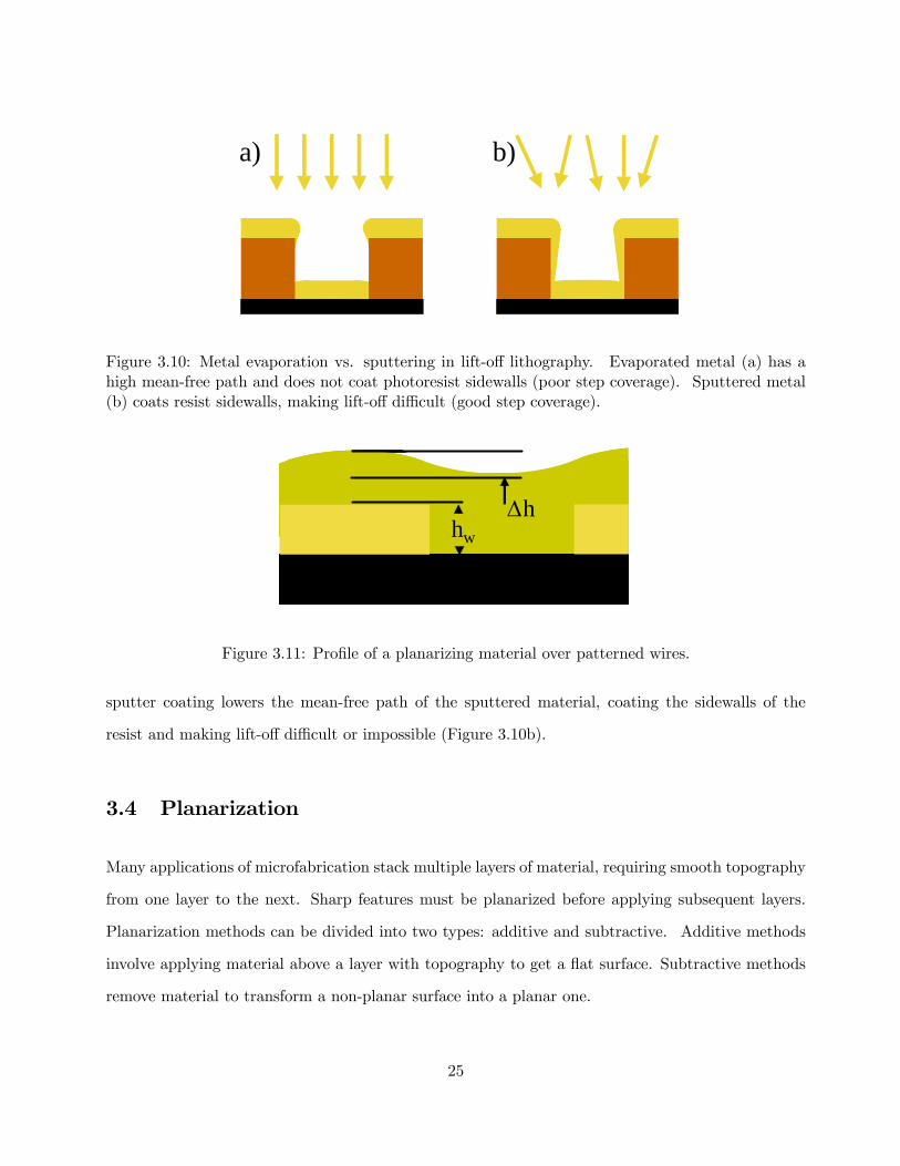
a) b)
Figure 3.10: Metal evaporation vs. sputtering in lift-off lithography. Evaporated metal (a) has ahigh mean-free path and does not coat photoresist sidewalls (poor step coverage). Sputtered metal(b) coats resist sidewalls, making lift-off difficult (good step coverage).
hwΔh
hwΔh
hwΔh
Figure 3.11: Profile of a planarizing material over patterned wires.
sputter coating lowers the mean-free path of the sputtered material, coating the sidewalls of the
resist and making lift-off difficult or impossible (Figure 3.10b).
3.4 Planarization
Many applications of microfabrication stack multiple layers of material, requiring smooth topography
from one layer to the next. Sharp features must be planarized before applying subsequent layers.
Planarization methods can be divided into two types: additive and subtractive. Additive methods
involve applying material above a layer with topography to get a flat surface. Subtractive methods
remove material to transform a non-planar surface into a planar one.
25

Planarization is quantified by the degree of planarization (DOP), defined as [53]:
DOP = 100×∙1− ∆h
hw
¸(3.1)
where ∆h is the deviation in the surface topography and hw is the height of the underlying features
(Figure 3.11). Degree of planarization can be defined globally across the wafer or locally. For
most microfabrication applications local planarization is the most important, since films must be
continuous over changes in topography.
The simplest way to planarize is additively, using a spun-on material such as photoresist, poly-
imide, benzo-cyclo-butene (BCB) or spin-on glass (SOG). These materials exhibit a range of DOP
values, with photoresist and SOG being the least planarizing, and polyimide and BCB the most.
Photoresist is conformal to the underlying topography and acts simply to smooth sharp edges. Poly-
imide and BCB are low-dielectric planarizing polymers that are spun on with a range of thicknesses
from < 1μm to > 10μm. Two important characteristics of a planarizing spin-on layer are flow and
shrinkage [54]. Materials that exhibit high flow are better planarizers since the polymers flow over
wire edges to fill gaps. When planarizing materials are cured, they shrink as solvents are evaporated,
decreasing the flatness of the surface. Polyimides with a high fill content and BCB are therefore
better at planarization because they exhibit less shrinkage.
Subtractive planarization methods include chemical-mechanical planarization (CMP) and etch-
back. CMP uses abrasives such as SiO2 in a slurry with a corrosive alkali combined with an absorbent
pad rotating pad to remove material from a surface [55]. The wafer sits on a polishing head, which
pushes against the pad containing the slurry. The rate and uniformity of material removal is depen-
dant on the type of slurry, the rotation speed, the pressure of the polishing head against the pad,
and the temperature. Degree of planarization using a CMP process can be as good as 100%, both
locally and globally.
Etch-back planarization combines additive and subtractive methods, and is most often used to
obtain a flat oxide or nitride passivation layer [47]. A layer of oxide/nitride is coated with spin-on
glass (Section 5.3.1). The SOG acts as a gap-filler and crude planarization layer. A reactive ion
26

etch (RIE, see Section 3.5) is used to selectively remove material from the surface. By adjusting the
etchant gases the ratio of etch rates between SOG and oxide/nitride can be controlled. The bilayer
is then etched back until a smooth surface results.
3.5 Reactive Ion Etching
Reactive Ion Etching (RIE) combines chemical and physical processes to etch bulk material or pat-
terns in a material defined by a mask [47]. For our process, RIE is necessary for selectively removing
material on multilayer chips to expose the underlying trapping wires. Etching takes place in a re-
action chamber with an inert gas (such as Ar) at a pressure between 10−2 and 1 torr. A potential
between two plates generates a plasma in the inert gas, similar to a sputtering system (Section 3.2.2).
An etchant gas mixture of gases is injected into the chamber at a controlled rate.
The chemical process is driven by reactions between etchant radicals and the material. Collisions
with energized particles in the plasma dissociate the etch gas into reactive species that diffuse through
the plasma to reach the surface. There, the radicals adsorb to the surface and chemically react. The
reaction products are volatile gases which desorb from the surface to be pumped out of the chamber.
The physical part of the RIE process is similar to sputtering. The potential in the chamber
accelerates ions towards the surface of the substrate which sits on the cathode. The bombarding ions
drive material from the surface through collisions. Here etch rate is dependant on the kinetic energy
of the impacting ions and not on chemical reactions. An etch based entirely on ions is therefore
highly non-selective between the material to be etched and the masking material.
Purely chemical processes occur at higher pressures (∼ 1 torr), where the short mean free path
of the diffusing radicals causes isotropic etching. In contrast, purely physical etching occurs at lower
pressures (∼ 10−3 torr) and is much more anisotropic due to the long mean free path. RIE combines
these two processes at intermediate pressures by varying free radical and ion concentrations to control
etch rates and edge profiles.
Etch gases (O2, SF6, CF4, H2, etc.) are chosen based on chemistry between the radicals formed
27

in the plasma and the material to be etched. The radicals either do not react with the masking
material, or react at a much slower rate.
At the lower pressures required to attain straight sidewalls through anisotropic etching a simple
parallel plate RIE setup is not efficient at generating a high density plasma. Etch rates are therefore
low, since less free radicals are formed. By increasing the potential to generate a denser plasma,
the etch becomes more physical and can to lead loss of selectivity and even to sputtering. However,
energy can be inductively coupled into the plasma at lower pressures through a coil carrying rf power.
This technique is known as inductively coupled plasma (ICP) and is commonly used for low pressure
anisotropic etching with high etch rates [50].
3.6 Wirebonding
Wirebonding is a method of integrating chip-scale devices with external electrical connections using
thin wire or ribbon [56]. Wirebonders use a combination of heat, pressure and ultrasonic energy to
form welds between the wires and bond pads, without the need for a solder. The wires, usually Au,
Al or Cu, are commonly 25μm in diameter, allowing for many welds in a small area.
The two most common methods of wirebonding are ‘wedge’ bonding and ‘ball’ bonding [57].
When wedge bonding, the wire is fed through a hole in the back of the wedge tool and passes
beneath the bonding foot of the tool. There, the wire is pressed between the foot of the tool and
a bond pad, which may be heated. Ultrasonic energy is applied to the tool to break down surface
impurities at the interface between the wire and the bond pad. The mechanism of wedge bonding is
as follows:
1. Position wedge over first bond pad.
2. Press wire between wedge foot and bond pad and apply ultrasonic energy to wedge.
3. Lift wedge and kink wire.
4. Move wedge to second bond pad while feeding out wire.
5. Make second bond.
28

6. Lift wedge and tear wire.
The most important parameters to wedge bonding are bond force, ultrasonic power and the
duration of the power delivery. Each of these can be controlled by the wirebonder. Wire size can
vary from < 25μm to > 500μm diameter, depending on the power required for the application.
Ribbon is also used, which provides a large bond surface for better impedance matching in high
frequency applications.
3.7 Scanning Electron Microscope
For imaging sub-micron sized features such as the grain structure of the atom chip surface, optical
microscopes are no longer sufficient. Electron microscopes replace photons with a beam of electrons
to image small features. A scanning electron microscope (SEM) raster scans a focussed beam of
electrons across a surface, generating secondary and back-scattered electrons which are re-emitted
from the material [58]. As the beam is scanned a portion of these electrons are detected to create
a two dimensional image of the surface. SEM can attain images with much more resolution than
diffraction-limited optical microscopes.
When a beam of electrons impinges on a surface, elastic and inelastic interactions take place
to produce electrons and photons with a range of energies. At the top 1-10Å, Auger electrons are
generated and emitted [59]. Beneath that secondary electrons are formed and, at greater depths,
back-scattered electrons. Emitted electrons are detected either off-axis to the incident beam or axially
with an in-lens detector.
Most commonly, SEM measures the secondary electrons emitted from the surface at < 50 eV
and back-scattered electrons (energies > 50 eV) [60]. Secondary electrons are formed when primary
electrons collide with atoms in the surface and lose energy (SE1), or through collisions between atoms
and back-scattered electrons (SE2). These atoms emit electrons which have a probability of escaping
from the surface of the material. The interaction region has the area of the initial electron beam and
29

zBSE
SE
AE
PE
Figure 3.12: Depth profile of interaction regions in SEM to generate Auger electrons (AE), secondaryelectrons (SE) and back-scattered electrons (BSE) from a beam of primary electrons (PE).
the escape depth, ze, of primary electrons is no more than 10 nm, giving secondary electron detection
a very high resolution.
Image contrast with SE1 and SE2 electrons is achieved through the dependence of secondary
electron yield on the surface topography. At inclined surfaces the incident electrons have a longer
path length within the escape depth allowing more secondary electrons to be emitted than at a
perpendicular surface. The SE yield has a 1/ cosϕ dependence with tilt angle, ϕ. SE2 electrons have
an additional material-dependant contrast since the back-scattered electrons that generate them have
a probability of reflection that scales with the atomic number, Z [50].
The electron beam is generated either with a filament or by field emission and focussed with a pair
of magnetic condenser lenses and apertures [50]. In order to maximize resolution, the astigmatism
of the two lenses must be minimized and the two apertures must be aligned.
For the measurements in this thesis I have used two SEMs. The Watlab SEM (LEO 1530,
www.smt.zeiss.com/leo) is capable of very high resolution and can be used to image the grain
structure of metal surfaces (see Figure 5.16 for an example). The G2N SEM (Hitachi S-3000N,
30

www.hitachi.com) has lower resolution, but allows for the sample to be tilted up to 90 from hori-
zontal (see Figure 5.6 for an example).
3.8 Atomic Force Microscope
An atomic force microscope (AFM) scans a cantilever stylus over a surface and measures the deflection
of the cantilever as a result of the force between the stylus tip and atoms in the surface [61]. This
information is then used to map the surface topography or other surface features such as magnetic
domains [62]. The dominant force used in AFM is from the intermolecular potential that is repulsive
at close distances and attractive at larger distances (from van der Waals forces). AFM operates in
one of three modes: contact, non-contact and tapping, which are explained below. The cantilever is
raster-scanned using x and y-piezos. A laser reflected from the top surface of the cantilever into a
position sensitive detector monitors the deflection of the tip [63].
While SEM produces high resolution two-dimensional images, AFM functions in all three dimen-
sions. It is useful in our application for measuring surface roughness and topography.
In contact mode, the tip is dragged across the surface of the sample and the stylus tip is deflected
due to the repulsive forces. The topography measurement can be made in either constant height
mode or constant force mode. The former scans the tip across the surface and measures the can-
tilever deflection. The latter employs a feedback loop to keep the tip-surface force constant (i.e. no
deflection) by varying a z-piezo. In both cases, an attractive force is present due to capillary action
from a thin water layer.
Non-contact mode measures cantilever deflection in the attractive van der Waals regime, tip-
surface distances of 50-100 Å. Deflections here are much smaller than in contact mode, so the can-
tilever is oscillated at its resonant frequency and small variations in resonance from the attractive
force are measured instead of measuring deflection directly. Non-contact AFM is useful for soft
surfaces that may be damaged by the sharp tip, such as polymer films.
Early AFM styli were made from bonding diamond shards onto glass beams or wires or from
31
etched wire tips [61], [64]. Today, styli are commonly fabricated from etched Si or Si3N4 with a
reflective layer on the backside for optical imaging. The shape of the tip and spring constant of
the cantilever is selected for the AFM application. Sharper tips achieve higher resolution for two
reasons. First, the narrower width allows them to penetrate deeper into features and the sharper
tip has less atoms interacting with the surface. Duller tips are more durable, suitable for larger scan
areas. Contact mode uses cantilevers with low spring constants while non-contact mode requires
cantilevers with high spring constants for resonant frequencies of hundreds of kHz.
One disadvantage of AFM over SEM is that, while AFM is much more suitable for topographic
measurements, SEM images lateral features with more accuracy. The piezos used for raster scanning
in AFM have nonlinearity and hysteresis that distort lateral features and when changing scan lengths,
one must wait for the piezos to relax before taking an image.
3.9 Dektak Surface Profiler
Like an AFM, a Dektak surface profiler is a device for measuring surface topographies. However, it
is a simpler device and can scan over larger vertical and horizontal scales. The Dektak, like other
profilometers, uses a diamond-tipped metal stylus coupled to a transducer [65]. The sample to be
measured sits on a translation stage beneath the tip and, as the sample is scanned, the vertical
deflections of the stylus generates an electrical signal. The diamond tips are hemispherical, typically
12.5μm in radius, small enough to measure most microfabricated structures, but blunt enough to
minimize scratching soft films such as polymers [66]. Still, the smallest features that can be measured
are limited by the tip radius. As an example, to reach the bottom of a groove with a depth of 1μm
using a tip with a 12.5μm radius, the edges of the groove must be more than 10μm apart.
32

Chapter 4
Atom Chip Design
Our Rydberg atom experiments require two atom chip designs to be fabricated, which will be called
“Chip 1” and “Chip 2” for the remainder of this thesis. Chip 1 is intended primarily for the
development of magnetic trapping, as well as rudimentary Rydberg atom experiments. It consists
solely of a set of trapping wires on a substrate. Chip 2 has a metal surface above the trapping wires,
separated by a dielectric film. This metal surface is specific to the study of Rydberg atom-surface
interactions and has other important uses which are explained in Section 4.5.
To put the role of the atom chips into perspective, this chapter begins with a description of the
experimental setup. Following this, the key elements of the chip design are presented along with a
review of other groups’ work to justify design choices.
4.1 Experimental Setup
The atom chip is mounted on a machined Macor block in an ultra-high vacuum (UHV) chamber at
a base pressure of about 1 × 10⁻⁹ torr. A background of 87Rb is introduced to the chamber and is
cooled and trapped by a magneto-optical trap (MOT) that uses a combination of optical radiation
and a magnetic quadrupole field1. A conventional MOT uses three pairs of counterpropagating laser1A detailed reference for MOTs can be found in [12].
33

U-wire
Z-wire
Macor
1 cm
Figure 4.1: Submount for atom chip. Macroscopic U-wire and Z-wire are imbedded in a Macorblock.
beams to cool the atoms. However optical access is impeded close (within a few mm) to the chip
surface. A solution to this problem is to use the surface of the atom chip to reflect two of the
incoming MOT beams. This is known as a reflection MOT, or mirror-MOT (MMOT), a term first
used by Reichel et al. [5].
The quadrupole field used for the MMOT is formed by combining the fields from two pairs of
external coils with a U-shaped copper wire embedded in the Macor beneath the chip (Figure 4.1).
The U-wire has a rectangular cross section, optimized for forming a quadrupole field close to the
chip’s surface, and is based on the design by Wildermuth et al. [67].
To load atoms from the MMOT to the magnetic chip trap a process adapted from Kasper et al.
[68] is used. The atoms are first optically pumped into a weak field-seeking state and transferred
into an intermediate magnetic trap formed by a Z-shaped wire (also embedded beneath the chip)
and external coils. The lasers are switched off, leaving a purely magnetic trap. Then the atoms are
evaporatively cooled using rf radiation while compressing the trap. The cold atoms that remain are
transferred to the chip by ramping down the current in the Z-wire and increasing the currents in the
atom chip wires.
34

Once the atoms have been loaded into the atom chip trap, they can be positioned within a few
μm of the chip surface and optically excited to Rydberg states through a combination of lasers and
microwave radiation. Interactions between the Rydberg atoms and the surface of the chip can occur,
as introduced in Section 2.2. These will be probed using spectroscopy of the initial optical excitation,
or by driving further microwave transitions between Rydberg states [69]. Effects of the atom-surface
interactions can be detected through selective field ionization (SFI).
4.2 Trap Geometry and Layout
Figure 4.3 and Figure 4.4 show the layout of Chip 1 and Chip 2, respectively. The trapping region is
a 4mm long strip of five parallel wires at the centre of the chip. The centre wire of both Chip 1 and
Chip 2 is 7μm wide, sufficiently narrow to form a tight trap close to the wire. It is an H-shaped wire,
allowing it to function as either a Z- or U-wire (C1−4). A 7μm wide U-shaped wire sits on either
side of the centre wire, separated from the centre wire by a 7μm gap (UI1−2, UI3−4). This pair of
wires can be used to generate the bias field when trapping with the centre wire (Figure 4.2b). They
can also be used in cooperation with the centre wire to load the chip from the Z-wire trap with the
three carrying copropagating currents.
A 14μm wide U-wire neighbours each of the inner U-wires (UO1−2, UO3−4). On Chip 1 these
outer U-wires are separated from the inner U-wires by 7μm. The outer U-wires are used for gen-
erating the bias field for loading the atoms from the Z-wire magnetic trap to the chip trap (Figure
4.2a). Chip 2 has an updated design, with the outer U-wires positioned further from the three centre
wires (300μm). The larger spacing allows a tighter trap to be formed at distances of > 100μm to
facilitate loading the trap from the Z-wire trap. Each of the wires ends in a bond pad at the edge of
the chip. The use of the ground pads, G1 and G2, is explained in Section 5.4.
The dimensions of all chips are 2.02×2.02 cm, constrained to the largest size that will fit through
a 2.75 ” Conflat port on the vacuum chamber.
35

a) b)
Figure 4.2: a) Trap formed by centre wire (C) and inner U-wires (UI) with outer U-wires (UO)providing bias field. b) Trap formed by centre wire (C) with inner U-wires (UI) providing bias field.
25 μm
2.5 mm
C1
C2
C3
C4
UI1
UI2
UI3
UI4
UO1
UO2
UO3
UO4
G1
G2
Figure 4.3: Layout of Chip 1 with wires labeled (C: centre wire, UI: inner U-wires, UO: outer U-wires,G: ground contacts). Arrows indicate current paths of C1, UI1 and UO1. Magnified view of the endof the centre wire strip is shown at right.
36
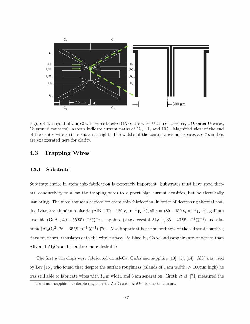
C1
C2
C3
C4
UI1
UI2
UI3
UI4
UO1
UO2
UO3
UO4
G1
G2
2.5 mm 300 μm
Figure 4.4: Layout of Chip 2 with wires labeled (C: centre wire, UI: inner U-wires, UO: outer U-wires,G: ground contacts). Arrows indicate current paths of C1, UI1 and UO1. Magnified view of the endof the centre wire strip is shown at right. The widths of the centre wires and spaces are 7μm, butare exaggerated here for clarity.
4.3 Trapping Wires
4.3.1 Substrate
Substrate choice in atom chip fabrication is extremely important. Substrates must have good ther-
mal conductivity to allow the trapping wires to support high current densities, but be electrically
insulating. The most common choices for atom chip fabrication, in order of decreasing thermal con-
ductivity, are aluminum nitride (AlN, 170− 180Wm−1K−1), silicon (80− 150Wm−1K−1), gallium
arsenide (GaAs, 40− 55Wm−1K−1), sapphire (single crystal Al2O3, 35− 40Wm−1K−1) and alu-
mina (Al2O32, 26− 35Wm−1K−1) [70]. Also important is the smoothness of the substrate surface,
since roughness translates onto the wire surface. Polished Si, GaAs and sapphire are smoother than
AlN and Al2O3 and therefore more desirable.
The first atom chips were fabricated on Al2O3, GaAs and sapphire [13], [5], [14]. AlN was used
by Lev [15], who found that despite the surface roughness (islands of 1μm width, > 100 nm high) he
was still able to fabricate wires with 3μm width and 3μm separation. Groth et al . [71] measured the2 I will use “sapphire” to denote single crystal Al2O3 and “Al2O3” to denote alumina.
37

resistive heating of wires fabricated on Si, GaAs and sapphire to determine which was most suitable
for the high current densities required by atom chips. They concluded that, due to its higher thermal
conductivity, Si was the preferred substrate. Si requires a passivation layer to provide the electrical
isolation necessary for the high potential differences between wires. Passivation layers, SiO2 and
Si2N3, have poor thermal conductivity however and there is trade-off between electrical isolation and
thermal conductivity between the wires and the substrate. A 20 nm thick SiO2 layer was found to
be sufficient in both regards.
We chose Si as the substrate for our chips based on the above, but also due to its relative
affordability and availability.
4.3.2 Wire Material
To achieve the required current densities, the atom chip wires must be made of a highly conductive
material. Metals (Au, Ag, Cu) are ideal, both for high conductivity and ease of fabrication. The
use of Au is most common, since it is much less susceptible to oxide formation than Cu and Ag.
Evaporated Cu has been used by Lin et al . [21], however the wires were coated with a Ti/Pd/Au
tri-layer to protect the copper from oxidation.
Dikovsky et al . [72] showed that magnetic field fluctuations are material dependant and can be
reduced using alloys of Ag and Au.
Gold (Au) is a non-reactive metal and exhibits poor adhesion to substrates such as sapphire and
SiO2. An intermediate adhesion layer is required before depositing a Au layer. Cr and Ti have been
used by the majority of atom chip groups.
Our chip wires are fabricated using Au as the current-carrying material. Chip 1 uses a layer of
Cr as the adhesion layer. Chip 2, however, must undergo high temperature processes for subsequent
layers (350 C, Section 5.3.2). Cr diffuses into Au at these temperatures (Section 2.3.2), requiring
a different material for the adhesion layer. A Ti adhesion layer with a Pd buffer layer was chosen,
since the Ti reacts with the Pd at the Ti/Pd interface and does not diffuse through into the Au [44].
38

4.3.3 Wire Patterning Method
The method of depositing and patterning the trapping wires is extremely important to the perfor-
mance of the chip. Conventional methods used in atom chip fabrication are introduced in Sections
3.2 and 3.3.3. The choice of fabrication method depends on the size of the wires and the acceptable
surface and edge roughness.
Electroplating (Section 3.3.3) allows for wire thicknesses > 10μm that can carry high currents
(> 1A). Lev [15] has electroplated Au wires 14μm thick and 50μm wide over a Cr/Au seed layer
using Clariant AZ9200 negative resist as a mould. A drawback of electroplating is larger grain size,
which leads to roughness of wire edges and surfaces. Rough wires lead to a distorted current flow
that causes corrugations in the magnetic field (see Section 2.1.3). A typical electroplated Au film
has grains with an average diameter of around 1μm or greater, although Koukharenko et al . [73]
report an optimized electroplating process with an average grain diameter of < 90 nm. A second
disadvantage to using sputtered wires is that the etch step used to remove the seed layer roughens
the wire surfaces. This roughness leads to poor reflectivity, making it difficult or impossible to form
a MMOT. Additional layers must be applied to obtain a reflective surface (see Section 4.4). For
Chip 1 electroplating was therefore not suitable due to surface roughness and for Chip 2 due to edge
corrugations.
Wires can be defined by uniformly metallizing a substrate and then patterning the metal into wires
using wet chemical etching (Section 3.3.3) [73], [15], [21]. Etching is advantageous over electroplating
when a reflective surface is required, since the metal can be deposited using evaporation or sputtering.
Only a thin layer of positive photoresist is required to define the pattern, leading to a simpler process
compared to the thick mould required for electroplating. The primary disadvantage of wet etching is
isotropic undercut, which limits the maximum aspect ratio that can be achieved. Wire edges defined
by wet etching are also rough (see Section 5.3.3), which would possibly lead to magnetic potential
roughness similar to electroplated wires.
Lift-off photolithography (Section 3.3.3) is less conventional in standard microelectronics fabri-
cation but is frequently used for fabricating atom chips. Atom chip wires have been patterned using
39

optical resists [71], [15] and electron beam resists [27], [74]. In both cases, the benefit of using the
lift-off method is extremely smooth wire edges. Since the wire edges mimic the edge of the resist,
roughness is limited only by the grain size of the metal (< 80 nm [71])3. A second advantage of
lift-off is the ability to pattern narrow features. Lift-off with optical resists can achieve wire widths
of 1μm and electron beam resists can be used to pattern features an order of magnitude narrower
[6]. The drawback of lift-off compared to electroplating is aspect ratio. Film thickness is generally
limited to 1− 2μm, since thicker films can make contact with the sidewalls of the resist. The degree
of undercut of the resist sidewall is therefore often what limits film thickness. That said, Groth et al .
[71] have reported fabricating wires up to 5μm thick using Clariant AZ 5214E spun at a low speed.
Alternative patterning techniques are ion milling and focussed ion beam (FIB). Lev [15] used ion
milling for atom chip prototypes by patterning a positive photoresist over a uniform film and etching
using Ar in an ICP chamber. Ion milling is capable of producing smaller features than wet etching
and the edge roughness is comparable to that of the photoresist. Della Pietra et al . [75] used a FIB
system4 to polish the edges of a section of wire originally fabricated with lift-off lithography. The
wire edges were smoother than those that had not been polished, as was the potential roughness.
Considering the possible methods for fabricating the trapping wires, we chose lift-off photolitho-
graphy for both Chip 1 and Chip 2. This method provides adequate aspect ratios and gives smooth
wire edges and surfaces. Techniques such as ion milling and FIB require equipment that was un-
available to us.
4.4 Planarization
To meet the requirement of a flat interaction surface and mirror, a thin, insulating planarization
layer is needed. Atom chip groups have used various methods to obtain planar surfaces above the
trapping wires. Besides the standard techniques outlines in Section 3.4, atom chip groups have used
other more creative methods.3Grain size is dependant on film thickness (Section 2.3) and deposition conditions.4FIB uses a focussed beam of ions from a liquid metal source to mechanically etch patterns in a film [47].
40

a) b) c)
Figure 4.5: Three methods of achieving a planar surface above atom chip wires: a) spin-coated layer(photoresist, polyimide, BCB), b) mirror transfered from optical flat and epoxied to chip using wirespacers, c) embedded wires in grooves etching into substrate.
Early chips by Reichel et al . [5] used a 200 nm Ag mirror sputtered on photoresist spun over elec-
troplated wires. The wire dimensions were 3.8μm×300μm and the photoresist thickness was around
1μm. The advantage of this method is the simplicity, since spinning and patterning photoresist is
a standard fabrication process and unwanted areas of resist can even be removed with acetone and
a swab. Unfortunately, photoresist is conformal to the topography of the underlying surface, and so
in this case it acted only as an insulating layer between the wires and metal mirror.
To obtain a planar surface, later chips by Reichel et al . [76] utilized a transfer technique where
the reflective layer, again silver (250 nm), was sputtered on an optically flat substrate. The exposed
silver face was then epoxied to the chip surface with Epotek 353ND using wires with 25μm diameter
as spacers. After curing, the optical flat was peeled off of the silver mirror. This method is very
similar to techniques used to fabricate ultra-smooth templates for SPM [77] and for atom-surface
studies [78]. The optically flat template substrate can be float glass, mica, or even silicon coated
with photoresist. This method gives a very smooth, planar surface matching the roughness and
flatness of the template. For our application there is an important disadvantage to this technique.
The distance between the mirror and the wires is limited by the thickness of the epoxy. Epotek 353
has a minimum thickness of 25μm, which then restricts the trapped atom-wire surface distance to
25− 26μm.
An improvement to these methods is to coat the wires with a planarizing dielectric. Both poly-
imide and benzo-cyclo-butene (BCB) have been used to obtain flatter surfaces [15], [74], [79], [26].
41

Their application and patterning are compatible with standard clean room practices and fabrication
equipment. Lev [15] used single and multiple layers of spin-coated polyimide (HD Microsystems PI
2560 @ 2000 RPM) to planarize a chip with 12-14μm tall electroplated wires. The metal contacts
of the underlying wires were made accessible by peeling away areas of the polyimide film. Similar
to chips made using a photoresist isolation layer, these chips were not sufficiently planar to form a
mirror-MOT due to a 50% DOP leaving 6 − 8μm corrugations. Lev notes that these results arise
from the application of multiple coats of polyimide before curing, and suggests that a full cure be-
tween layers should improve planarization. Spinnable polyimide is composed of a polyamic acid in
an organic solvent. As the polyimide is cured the solvent evaporates, which causes the film to shrink
in thickness by as much as 50% [54]. Therefore a polyimide layer that had 100% planarization before
curing would only be 50% planar after curing. Applying a second layer after curing would give a
75% planar surface, and so on.
Nirrengarten et al . [79] coated microfabricated Nb wires with a photodefinable BCB (Dow Chemi-
cals XU35133) and Schumm et al . [26] used BCB to planarize electroplated Au wires. BCB is a highly
planarizing material as it exhibits very low shrinkage during cure. Also, because it is photodefinable,
patterning the film is simplified compared to materials which must be etched after a full cure. A
disadvantage of BCB is that it must be cured in an inert environment as it is prone to oxidation.
Treutlein et al . [74] proposed a method of embedding the trapping wires in the substrate itself by
first etching grooves using RIE and then filling them with evaporated metal. Negative photoresist
could be used as both an etch mask and a lift-off sacrificial layer, minimizing the number of aligning
and patterning steps. After lift-off, the surface would be highly planar, as long as the metal layer was
deposited at the same thickness as the groove depth. The insulating layer between the wires and the
mirror could then be thin, since it would only be required for electrical isolation. Polyimide, BCB,
SiO2 or even photoresist would be suitable. This method requires a substrate with high resistivity,
since the wires must be isolated from each other. High resistivity silicon, sapphire and AlN can be
etched using RIE processes [49], [80], [81] although the latter two materials require patterned metal
etch masks. A substrate with low resistivity can be used if an insulating oxide or nitride layer is
deposited in the trenches before the wires. A problem that must be overcome is the roughness of
42

a) b)
Figure 4.6: Planarization of a) a single wire versus b) a gap.
the groove surface an sidewalls, which would lead to roughness of the edges and surface of the wires
filling the grooves . The RIE process therefore has to give very smooth sidewalls and surface.
Spun-on planarizing materials act better as gap fillers than as global planarizers. The above
methods were developed to planarize chips with isolated wires separated by large gaps. If wires are
instead defined by thin gaps in an otherwise uniform metal layer, planarization with polyimide or
BCB, or even photoresist will be improved. Figure 4.6 shows how the wire spacing can affect the
surface topography of a planarizing film.
Based on the need for a thin planarization layer and the available equipment (no CMP), we chose
to use a spin-on planarization layer. Both spin-on glass (SOG) and polyimide were options (Sections
5.3.1 and 5.3.2). With either material, the layer is etched away from the perimeter of the chip to
expose the bond pads of the wire layer.
4.5 Shield
Besides acting as a reflective surface for a MMOT, the metal surface of Chip 2 is required to perform
other functions. Rydberg atoms are extremely sensitive to electric fields. The voltage drop due
to neighouring wire carrying 300mA of current at separations of 7μm would result in an electric
field sufficient to significantly effect the Rydberg atoms. The metal surface of the chip acts as an
electrostatic shield to protect the Rydberg atoms from the electric fields generated by trapping wires.
For the remainder of this thesis, I will refer to the surface layer as the “shield layer”.
43

The Rydberg atoms will interact with the surface of the shield layer, so it must be specifically
optimized for these interactions. As explained in Section 2.2, the Lennard-Jones shift due to dipole-
dipole interactions between a Rydberg atom and its image in the surface scales as 1/z3. If a cloud of
atoms were trapped at 2μm from the surface, a deviation in atom-surface distance of 1μm (i.e. the
height of the underlying wires) would result in an error in the Lennard-Jones shift of about 70 %. A
200 nm deviation would result in an error of just 25 %. Therefore, a planarized surface is extremely
important, with a local deviation of no more than 200 nm.
As mentioned in Section 4.1, using selective field ionization (SFI) to perform spectroscopy on the
Rydberg atoms requires a pair of plates to generate an electric field. The shield layer is to be used as
one of the two electrodes, with a metal plate acting as the other. By applying a voltage between the
shield layer and the plate, the Rydberg atoms can be ionized. The ions are then accelerated through
a hole in the plate to be detected by the MCP.
A significant loss mechanism in magnetic traps near surfaces is spin flips due to magnetic noise
from the surface material (Section 2.1.3). Thinner surface layers over insulators produce less noise
than thicker layers, which increases trap lifetime [22], therefore a thickness of 100 nm was chosen for
the shield layer.
The shield layer is fabricated by thermally evaporated Au with a Cr adhesion layer and patterned
using lift-off lithography. While the edge quality is not important for this layer, etching is not a
suitable method. If the etching method were used, the entire chip would be metallized including the
exposed bond pads of the underlying trapping layer.
The problem of performing Rydberg atom spectroscopy in the vicinity of patch fields (Section
2.2) must also be considered. Over a polycrystalline surface with average grain diameter and spacing
w, the average shift of Rydberg energy levels due to the electric field scales with w2 (at distances
z À w). Smaller grain size is important to minimize patch effects, which can be accomplished by
thermal evaporation at room temperature at a moderate deposition rate (see Section 5.4.1). Grain
size also increases with film thickness which further justifies choosing a thickness of 100 nm.
44

Si (with thin SiO2) Au (with adhesion layer) Polyimide/SOG
Ribbon bond
Figure 4.7: Schematic cross section of Chip 2 design.
4.6 Summary
This chapter has discussed two atom chip designs. Chip 1 is intended as a trial chip, to allow
familiarization with MMOT and magnetic trapping techniques and to perhaps perform rudimentary
measurements of Rydberg atom-surface interactions. Chip 2 has a shield layer above the wires,
separated by a planarizing dielectric layer. This chip is much more suited to studies of interactions
between Rydberg atoms and metal surfaces.
Chip 1 is fabricated on a Si substrate coated with a thin layer of SiO2 as an insulator. The chip
is uniformly coated with Au (with Cr as an adhesion layer) except for gaps which define the wires.
The wires are patterned using lift-off photolithography.
The wire layer of Chip 2 is fabricated in the same manner as Chip 1 except for a Ti adhesion layer
and Pd diffusion barrier to keep the Ti from diffusing in the Au during subsequent high temperature
processes. The design of the wire pattern of Chip 2 is updated from that of Chip 1, with the outer
U-wires spaced further from the inner set of wires to expand the distance range at which atoms can
be tightly trapped. Above the wires is a spin-coated planarizing dielectric layer (polyimide) which is
patterned to reveal the bond pads. Finally, a Au layer (with Cr adhesion layer) coats the dielectric.
This layer is a mirror for the MMOT, an electrostatic shield, an electrode for SFI and the surface
for interaction studies. A cross section of the Chip 2 design is shown in Figure 4.7.
45

Chapter 5
Atom Chip Fabrication
This chapter describes in detail the methods and results of fabricating the two atom chips designs.
The first, Chip 1, is intended as a trial chip, consisting only of trapping wires and not the planarization
and shield layers. This chip is to be used to gain experience trapping atoms on chip and to perform
initial Rydberg atom experiments, which are expected to show the need for the second, multilayer
chip design. The second, Chip 2, is suited for the study of Rydberg atom-metal surface interactions.
In total, two chips with the Chip 1 design and five with the Chip 2 design have been fabricated.
Figure 5.1 outlines the general fabrication process and the related sections in this chapter.
Initially, fabrication steps were spread out over multiple facilities in multiple buildings across
campus. Wafer preparation and photoresist patterning took place at the a-SiDIC facility in Electrical
Engineering with the help of Czang-Ho Lee. Metallization was carried out in the fourth-year student
labs in the Department of Physics. Lift-off was done in Dr. Jan Kycia’s clean room. Early efforts at
planarization with spin-on glass were performed in various rooms in the Department of Chemistry.
This was not an ideal situation, and fortunately the Centre for Integrated RF Engineering (CIRFE)
facility in the Department of Electrical Engineering was made available. There, every process required
for fabrication could be carried out.
46
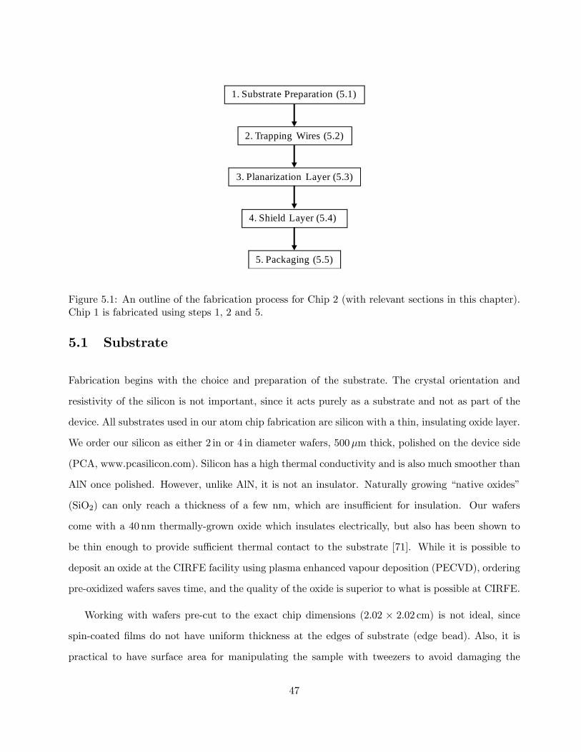
1. Substrate Preparation (5.1)
2. Trapping Wires (5.2)
3. Planarization Layer (5.3)
4. Shield Layer (5.4)
5. Packaging (5.5)
Figure 5.1: An outline of the fabrication process for Chip 2 (with relevant sections in this chapter).Chip 1 is fabricated using steps 1, 2 and 5.
5.1 Substrate
Fabrication begins with the choice and preparation of the substrate. The crystal orientation and
resistivity of the silicon is not important, since it acts purely as a substrate and not as part of the
device. All substrates used in our atom chip fabrication are silicon with a thin, insulating oxide layer.
We order our silicon as either 2 in or 4 in diameter wafers, 500μm thick, polished on the device side
(PCA, www.pcasilicon.com). Silicon has a high thermal conductivity and is also much smoother than
AlN once polished. However, unlike AlN, it is not an insulator. Naturally growing “native oxides”
(SiO2) can only reach a thickness of a few nm, which are insufficient for insulation. Our wafers
come with a 40 nm thermally-grown oxide which insulates electrically, but also has been shown to
be thin enough to provide sufficient thermal contact to the substrate [71]. While it is possible to
deposit an oxide at the CIRFE facility using plasma enhanced vapour deposition (PECVD), ordering
pre-oxidized wafers saves time, and the quality of the oxide is superior to what is possible at CIRFE.
Working with wafers pre-cut to the exact chip dimensions (2.02 × 2.02 cm) is not ideal, since
spin-coated films do not have uniform thickness at the edges of substrate (edge bead). Also, it is
practical to have surface area for manipulating the sample with tweezers to avoid damaging the
47

device. Wafers with 2 in diameter are ideal for fabrication, since they provide enough surface area
for the atom chip device, but also have a perimeter around the device for edge-beading or other
film thickness variations. Unfortunately, the industry standard in wafer sizes has long since increased
from 2 in and so the cost per unit area is higher. Costing slightly more than 2 in wafers, 4 in wafers
can be cut into four pieces with enough area for fabricating a chip on each. Since the substrate
dimensions do not have to be exact, 4 in wafers are cleaved into quadrants using a diamond scribe
and a ruler, scribing from the backside to protect the thin oxide.
Before patterning, the wafers are cleaned to remove any unwanted organic contamination that
may have occurred during storage. An effective method is the wet chemical ‘RCA 1’ clean, which
consists of a 5:1:1 ratio of H2O/NH4OH/H2O2 [82]. The procedure is as follows:
1. Add 100ml NH4OH to 500ml deionized (DI) water
2. Heat on hotplate to between 65 and 70 C
3. Add 100ml H2O2
4. Heat for 2min
5. Place samples in solution for 15min
6. Dilute with DI water under tap for 5min before removing samples
7. Rinse samples with DI water spray gun and dry with N2 gun
8. Dispose of diluted solution
It is important to prepare a fresh RCA 1 solution for each clean, since over time the H2O2
will deplete. The chemical clean will not etch silicon or thermally-grown silicon oxide unless the
concentration of H2O2 is too low [82], which can occur if stored for a prolonged period of time. Also,
organics can remain in the solution and contaminate subsequent cleans.
5.2 Trapping Wires
Of the three methods for fabricating metal patterns on a substrate (electroplating, etching and lift-
off), lift-off provides the smoothest feature edges (see Section 3.3.3). The lift-off lithography process
48

has three steps: photoresist patterning, metal deposition, and lift-off (Figure 3.9).
5.2.1 Mask
Of all the steps in fabricating the atom chips, making the masks for patterning photoresist is the
only one not performed at the University of Waterloo. Features smaller than a few tens of microns
require a professionally-made chromium mask, which can be patterned optically or with an electron
beam [48]. Our chromium masks were purchased from Applied Image (www.appliedimage.com) as
4 in square quartz or soda lime glass, 0.090 in thick. Soda lime glass has lower thermal stability
than quartz and during long exposures thermal expansion can cause feature widths to distort. In this
application, exposure times are short enough for thermal expansion to not be present. The masks
are made by first sputter-coating the plates with Cr (and a thin layer of a chromium oxide) and then
patterning a resist with a scanned ultraviolet laser so the Cr can be carefully etched. Upon arrival,
the masks are thoroughly inspected for defects. Figure 3 in Appendix III shows a short between two
wires caused by a patch of un-etched Cr on the mask.
With continuous use, patches of photoresist will occasionally stick to the mask. If this occurs, I
soak the mask in acetone and gently scrub with a clean room cloth while wet. Next it is rinsed in
methanol and then water and finally dried with a N2 gun. It is very important to only scrub the
mask while it is wet to avoid scratches. Over time, dried resist can build up along the edges of the
Cr features and is very difficult to remove with acetone and scrubbing. An RCA 1 clean is usually
sufficient to remove this residue. If not, the mask must be submitted to a “piranha etch”. This
extremely exothermic etch is a solution of 3:1 NH4OH:H2O2 and is named due to the ferocity with
which it attacks organics [83].
5.2.2 Photoresist Patterning
The three requirements of a photoresist for lift-off photolithography are:
• Good undercut (Figure 3.8b)
49

• Thickness greater than deposited film
• Smooth edges
For fabricating the trapping wires, three photoresists have been used: Futurrex NR1-3000PY
negative resist (www.futurrex.com), AZ Electronic Materials AZ 2035 nLOF negative resist and an
AZ LOR lift-off resist + AZ 3312 positive resist bilayer (AZ Electronic Materials, www.az-em.com).
Each of these resists meets the requirements for the lift-off process.
Early on, I used Futurrex NR1-3000PY since it costs the least, has a 3 year shelf life and is avail-
able in smaller quantities. Chips fabricated using this negative, I-line resist were patterned at the
a-SiDIC facility with the help of Czang-Ho Lee. As with any fabrication process, good results were
not immediate and troubleshooting was quite tedious due to limited access to the facility. The pri-
mary challenge with the Futurrex resist was the small developing time window. After 30 s the resist
appeared be visibly developed, but with any more than 5 additional seconds in the developer (Futur-
rex RD4) the lines began to peel off. This resulted in inconsistent patterns and a great deal of time
lost in stripping, cleaning and repatterning wafers. Once the a-SiDIC facility shut down and CIRFE
became available, I began patterning the trapping wires using AZ 2035 nLOF negative resist, pri-
marily because the I-line NR1-3000PY was incompatible with the unfiltered mercury discharge lamp
of CIRFE’s Oriel aligner (Oriel Model 87000 Series with Model 83210 stage, www.newport.com).
Students at the CIRFE facility patterned a series of wafers using a bilayer process of AZ LOR
and AZ 3312. The LOR is not photosensitive and acts purely as a sacrificial layer. A layer of LOR
is spun over the wafer and baked and then a layer of AZ 3312 is spun over that and baked. AZ
3312 is a thin, positive photoresist so its footprint matches the features on the mask. After the
AZ 3312 is exposed, it is developed in AZ 300 MIF. LOR is also sensitive to the developer and by
developing past the time required for the AZ 3312 the LOR is etched isotropically. The result is a
well-defined pattern of AZ 3312 sitting above an undercut LOR. Unfortunately, when developing the
bilayer process, problems arose with the LOR burning while baking, resulting in difficulty lifting off.
The AZ 2035 nLOF has proven to be the simplest and most consistent photoresist for patterning
the chip wires. Although it is an I-line resist, it still achieves good contrast and resolution with the
50

Figure 5.2: Spin curves for AZ 2000 nLOF series of photoresists ([84]).
broad UV spectrum of the Oriel aligner.
The process for AZ 2035 is:
1. Coat wafer with AZ 2035 resist using syringe dispenser and 0.45 μm filter
2. Spin at 2000 rpm for 30 s
3. Soft-bake at 110 C on vacuum hotplate for 60 s
4. Expose for 12 s with Oriel mask aligner
5. Post-exposure bake (PEB) at 110 C on vacuum hotplate for 60 s
6. Develop for 120 s in room temperature AZ 300 MIF developer, gently swirling and agitating
7. DI water rinse and blow dry with N2 gun
Photoresist Coating
Coating with photoresist is simplified by using a dispenser, which has a pedal-activated plunger to
push resist out of a syringe, through a filter and onto the wafer. To eliminate leaking when photoresist
is not being dispensed, it applies a back pressure. The dispenser must be set to give the minimum
back pressure so that after application it does not suck air up into the syringe. Care must also be
51

taken to avoid air bubbles in the dispensed resist, as these will lead to pinholes or “comets” in the
film. Dispensing the first drops of resist into a waste beaker and then moving the syringe above the
wafer without releasing the foot pedal ensures that air bubbles are eliminated from the final film.
I spin-coat in a closed-lid Teflon spinner (Laurell Technologies Corp., Model WS-500, www.laurell.com).
Spinning at 2000 RPM gives a final film thickness of between 3.5 and 4.0 μm, as measured with the
Dektak profilometer (Sloan Dektak I, see Section 3.9). The film thickness is also measured to be
uniform across the area of the chip.
Photoresist Exposure
The photoresist is exposed using the Oriel mask aligner in vacuum contact mode with a 500W Hg
lamp (Newport Corporation, Model 6285, www.newport.com). The wafer sits on a vacuum chuck
that can be raised and lowered mechanically, and translated and rotated using three micrometers.
The mask is held by vacuum on a hinged plate that is lowered flat above the wafer, where it rests
on two posts. After the mask is lowered, the wafer chuck is raised until the wafer comes into contact
with the mask, which can be observed by watching for a gap between the mask holder plate and the
posts. In this stage of fabrication, alignment is not important and the chip pattern can be visually
centred on the wafer. To ensure uniform contact between the mask and wafer, the space between
the mask plate and wafer stage is evacuated.
The optimal exposure depends on the spun thickness of the resist. Through trial and error, I
found 12 s of exposure to be ideal for resists spun at 2000 RPM.
Photoresist Development
In a new batch of AZ 300 MIF the unexposed areas develop away after about 30 s. I develop the
resist for an additional 90 s to etch into the sidewalls to increase undercut. After drying, I inspect
the wafer under a microscope to check the quality of the lines (undercut, edge roughness, residue
and poor adhesion). Undercut is visible as a darkening of the edges of the lines and the degree of
52

undercut can be roughly measured by focussing on the top and bottom surfaces of the resist. An
image of underdeveloped photoresist is shown in Figure 2 in Appendix III.
A cause of many defects in patterned photoresist is dried resist clinging to the mask. To ensure
smooth, unbroken lines the mask must be cleaned frequently either in a beaker of acetone or with a
RCA 1 clean (see Section 5.2.1).
5.2.3 Metal Deposition
For successful lift-off, the incident flux of metal particles must be perpendicular to the substrate
surface so that the resist sidewalls remain uncoated (Figure 3.10 ). Of the available metallization
methods (Section 3.2), thermal and electron beam evaporation are used for this reason. Sputter-
coating is not ideal, since the higher pressure shortens the mean-free path of the sputtered particles
and therefore they strike the surface at a large range of angles (sputtering is used, however, in
processes requiring metallization of a surface with varying topography).
The wires of both Chip 1 and Chip 2 are Au, with thickness of 1 to 1.5μm (see Section 4.3).
Chip 1 has a Cr adhesion layer (10-20 nm) and Chip 2 has a Ti adhesion layer with a Pd diffusion
barrier (20 and 50 nm respectively).
Thermal Evaporation System
I have used the thermal deposition system (Edwards Coating System E306A) for the majority of
metallizations. It is a diffusion-pumped bell jar system with the capability of evaporating from four
independent charges. The evaporator is used in a senior undergraduate lab for depositing tri-layer
thin film filters, although it has been substantially modified by Jeff Carter and myself to suit both
applications. Firstly, the distance between the charge and wafer was raised to 15 cm to provide a
more uniform metal thickness across the wafers. A mechanical shutter was added to shield the wafer
from impurities evaporated from the charge when current is first applied, and also from radiation
emitted while heating to the final deposition temperature. A copper housing surrounds the charges
to further contain the radiation, and has apertures to allow the evaporating material to pass through.
53

10 cm
Figure 5.3: Modified Edwards evaporator. This is located in the Department of Physics seniorundergraduate labratory area.
To cool the substrate during depositions, copper tubing for cooling water was run through the wafer
mounting stage.
Film thickness is measured using a quartz crystal oscillator which exploits the mass-dependant
resonant frequency of a quartz crystal. The crystal is placed in the deposition chamber in the path
of the charge so that it is coated with the evaporating material. The relationship between thickness,
t, and change in resonant frequency, ∆f , is effectively linear near the original resonant frequency,
given by [85]
∆f =ρt
C(5.1)
where ρ is the density of material evaporated onto the crystal and C is a constant, dependant on
the crystal and the geometry of the system (i.e. the angle and distance between the charge and the
54

2 cm
Figure 5.4: Quartz crystal and holder for film thickness monitoring.
crystal). The crystal (Kurt J. Lesker, P/N LI008010G10, www.lesker.com) is driven by a home made
oscillator circuit based on the design by Robinson et al . [85] and the frequency is read by a digital
frequency counter. The crystal holder (Kurt J. Lesker, P/N LI750211G1) is water-cooled since an
un-cooled crystal is easily heated by radiation from the charge and gives temperature dependent
resonant frequencies.
To calibrate the oscillator (i.e. the constant C, which varies for each material) I deposited
individual layers of each metal over wafers patterned with AZ 2035, and then measured the step
heights after lift-off using the Dektak for the Au and an AFM for the Ti and Pd (Section 3.8). The
ratio of the measured ∆f to the film thickness on the wafer is only an estimate. The actual thickness
has been found to vary by as much as 30 % from deposition to deposition. The cause of this variation
is that each time a thermal source is changed it is mounted in a slightly different position and even
during the deposition a source can shift its position due to thermal deformation. Since the crystal
holder is off axis from the mounted wafer, a portion of the incident metal vapour is shielded by the
aperture of the copper housing.
55

Chromium Deposition
I evaporate chromium from tungsten rods electroplated with a thick layer of Cr (Kurt J. Lesker, P/N
EVSCRW2). The rods are first broken in half by hand in order to fit between the current-carrying
copper posts and also to save material, as a rod is only used for one deposition. A machined copper
radiation shield surrounds the bottom and sides of the rod.
To remove organics and other contaminants from the surface of the rod, I first run 40A with the
shutter closed for 5 to 10min. I then increase the current at 10A /min up to 82 - 84A and hold
with the shutter opened slightly to expose the quartz crystal oscillator to the evaporating Cr. Once
the deposition rate is between 2 and 3Å / s I open the shutter and deposit Cr until ∆f = 500Hz
(about 10 nm), adjusting the current to keep the rate constant.
Titanium Deposition
I use 1/8 in diameter cylindrical pellets as the titanium charge (Kurt J. Lesker, P/N EVMT145EXE-
A). Titanium begins to evaporate at over 1200 C, requiring high resistance tungsten boats to reach
such high temperatures (Kurt J. Lesker, P/N EVSME5005W). The Ti pellets are cut in half to better
fit the small volume of the boat. Before mounting in the chamber, the ends of the boat are cut back
by 1/16 - 1/8 in in order to fit between the posts.
I start the deposition by running the Ti at 40A with the shutter closed for 5 to 10min and then
ramping up to 75A at 10A /min. At this point I increase the current by 2A /min with the shutter
open enough to expose the crystal oscillator. The current at which the Ti melts varies from run
to run, 75 to 95A due to inconsistent thermal contact between the boats and the pellets. At the
moment the Ti melts it begins evaporating, after which I adjust the current to maintain a deposition
rate of 5Å / s. A ∆f of about 500Hz gives a thickness of 20 nm, as measured with both the Dektak
profilometer and AFM.
After deposition the tungsten boat is brittle and can not be reused, so the current can be quickly
ramped down to zero. I let the system cool for at least 10min before beginning a subsequent deposition
process.
56
Palladium Deposition
Cylindrical pellets with 1/8 in diameter are also used as the source of palladium (Kurt J. Lesker, P/N
EVMPD35SHOT). Palladium begins to evaporate at close to 900 C. At this temperature, a tungsten
coil (Kurt J. Lesker, P/N EVB8A3030W) and Al2O3 crucible (Kurt J. Lesker, P/N EVC1AO) can
be used to heat the charge. A radiation shield made from two pieces of curved tungsten surrounds
the coil.
I first hold the coil at 40A for 5 minutes and then increase the current at 5A /min up to 75A.
At this current, the Pd is deposited at a rate between 4 and 5Å / s. I open the shutter and deposit
50 nm, corresponding to about 5000Hz change in oscillator frequency. Unlike the Cr and Ti sources,
the coil and crucible used for depositing Pd can be reused. I decrease the current by 5A /min to
ensure that neither the tungsten or Al2O3 crack. After shutting off the current I wait for at least
20min to allow the system to cool.
Gold Deposition
I have used 1mm-diameter wire and 1 Oz. bar as sources of gold for deposition, both with 99.99%
purity (Colonial Acres Coins, www.colonialacres.com). The sources are first cut to approximately
1 g pieces and then cleaned in acetone using an ultrasonic cleaner. The setup for evaporating Au is
identical to that of Pd, since both evaporate at similar temperatures.
The deposition rate for gold is important, more so than for the adhesion and intermediate layers.
The primary reason is heating. To deposit a 1μm film at a modest rate of 5Å / s, the surface of the
chip is exposed to the charge for over 30min. Although the wafer is water-cooled from the backside, it
can still get hot enough over this time to begin to damage the photoresist. Early deposition attempts
with such low rates resulted in burned and difficult to lift-off photoresist. I have deposited gold with
rates between 10 and 70Å / s with successful lift-off, although 35-50Å / s is most common.
In order to achieve and maintain high deposition rates two things are important. First, the
deposition rate is dependent on the surface area of the charge. High rates are maintained by starting
57

with 2 g of gold in the crucible. Also important is thermal contact between the coil and crucible.
Out of the package, the coils do not make sufficient contact with the bottom of the crucible and I
must bend them into shape before mounting. Even so, the bending and mounting process must often
be repeated to get the best contact.
I heat the gold at 40A for 5 minutes and then increase the current at 5A /min up to 76A or
until the deposition rate is between 35 and 50Å / s. Occasionally, a coil will compress while hot,
with neighbouring turns coming into contact. This lowers the resistance of the coil, causing a jump
in current. The current must then be adjusted to maintain the deposition rate. I deposit until ∆f
is about 100 kHz (1 − 1.5μm). After the deposition is complete, the current is ramped down at
5A /min so that the coil and crucible can be reused.
With a Cr, Ti or Ti/Pd adhesion layer, gold adhesion is very good and can withstand scratching
with metal tweezers and ultrasonic cleans.
5.2.4 Lift-off
The corresponding remover for AZ 2035 nLOF resist is AZ Kwik Strip. However, I do the first stage
of lift-off in warm acetone. Hot Kwik Strip is then used to remove baked-on resist residue. This
method keeps the Kwik Strip free of loose metal so that it can be reused. Often small flakes of
metal will stick to the gold surface in the acetone stage. Many of these flakes can be removed using
a low power ultrasonic clean in IPA. Ultrasonic cleaning also removes any thin metal film that may
have coated the photoresist sidewalls and clung to the wire edges (shown in Figure 4 in Appendix
III). The lift-off method is:
1. Place metallized wafer in beaker of acetone for 15—30min until metal has lifted off
2. In petri dish of acetone, carefully remove any remaining loose patches of metal
3. Rinse with isopropanol (IPA) and dry with N2 gun
4. Place in beaker of AZ Kwik Strip at 65 C for 30min to remove resist residue
5. Rinse in beaker of DI water
58

Figure 5.5: SEM image of trapping wires of Chip 1.
6. Place in petri dish of IPA and float in ultrasonic cleaner (Power: 4, Time: 1) to remove metalflakes and from surface
7. Rinse with IPA and dry with N2 gun
After the lift-off I inspect the chips with a microscope for photoresist residue and metal flakes. If
present, steps 4 through 6 can be repeated. Figure 5.5, imaged using the Watlab SEM, and Figure
5.6, imaged using the G2N SEM show SEM images of the fabricated wires of Chip 1.
5.2.5 Diffusion
After applying, curing and patterning polyimide planarization layers above the Cr/Au wires (Section
5.3.2), the resistances of the wires increase by up to 2.5 times their original values after three cures.
This is a problem because the resistive heating for a given wire current will also increase. It is likely
that diffusion of the chromium adhesion layer into the gold is the cause of the change in resistance
(see Section 2.3.2).
To eliminate the polyimide as a cause, I ran an uncoated chip through the three cure cycles
59

Figure 5.6: SEM image of kinks in wires of Chip 1.
with a maximum temperature of 350 C and measured the resistance after each using a four wire
probe. The centre wire had an initial resistance of 20.3Ω and rose to 36.3, 45.2 and 46.3Ω after one,
two and three cures. This effect was very similar to that measured by Madakson [41] and Munitz
et al . [40] who showed that resistance increases as the Cr diffuses into the gold film through grain
boundaries at temperatures above 300 C. Once it reaches the surface it forms and oxide, Cr2O3.
The resistance reaches a maximum as Cr saturates the Au film and then drops off once the Cr layer
becomes depleted. Eventually the majority of Cr is converted to Cr2O3 and the resistivity decreases.
The measurement of this chip indicated that resistance had reached the saturation point, and that
the Cr adhesion layer was not yet depleted.
I fabricate the Chip 2 chips using a Ti/Pd/Au tri-layer instead of Cr/Au. Titanium is a standard
alternative to chromium as an adhesion layer, although it is more expensive and difficult to thermally
evaporate. The palladium intermediate layer acts as a diffusion barrier between the titanium and
gold [44]. I repeated the measurement of the Cr/Au chip with a Ti/Pd/Au chip and also a Ti/Au
and Cr/Pd/Au chip, running them through three cure cycles without a polyimide coating. Figure
5.7 plots the change in resistance for the four different metallizations after each of the three cures.
60

0 1 2 3 -0.2
0
0.2
0.4
0.6
0.8
1
1.2
Number of Cures
ΔR
/R0
Cr/Au
Cr/Pd/Au
Ti/Au
Ti/Pd/Au
Figure 5.7: Change in resistance in centre wire after subjecting to polyimide cure cycles for Cr/Au,Ti/Au, Cr/Pd/Au and Ti/Pd/Au metallizations. The solid lines are to aid the eye.
The results for the Ti/Pd/Au chip are better than hoped, with the resistance after three cures
actually 1% lower than initially. The initial drop in resistance is likely due to the gold annealing.
This is not a strong effect at 350 C and was not observed in the other samples. In contrast to the
Ti/Pd/Au chip, the Cr/Pd/Au chip’s resistance increases by 55% suggesting that palladium is not
a sufficient diffusion barrier for chromium. Although the resistance of the Ti/Au chip rises by only
5%, the gold also begins to discolour to a dark magenta after the first cure and discolours further
during subsequent cures.
Another concern with diffusion is the buildup of oxide on the wire surface when making electrical
connections by wirebonding. The ability to make reliable, adherent bonds on Cr/Au bond pads with
gold ribbon was found to decrease significantly after a 400 C bake by Pan et al . [86]. In bond pull
strength tests, 100 % of the failures were due to the ribbon not sticking to the gold. They compared
this with bond pads made from Ti/TiN/Pt/Au which was then also annealed and none of the bonds
failed due to poor ribbon adhesion. My attempts to wirebond to the Cr/Au contacts after curing
met with the same problems. The wires can be easily pulled from the surface even if they appear to
stick after making the bond. In contrast, bondability to Ti/Pd/Au chips is excellent.
61
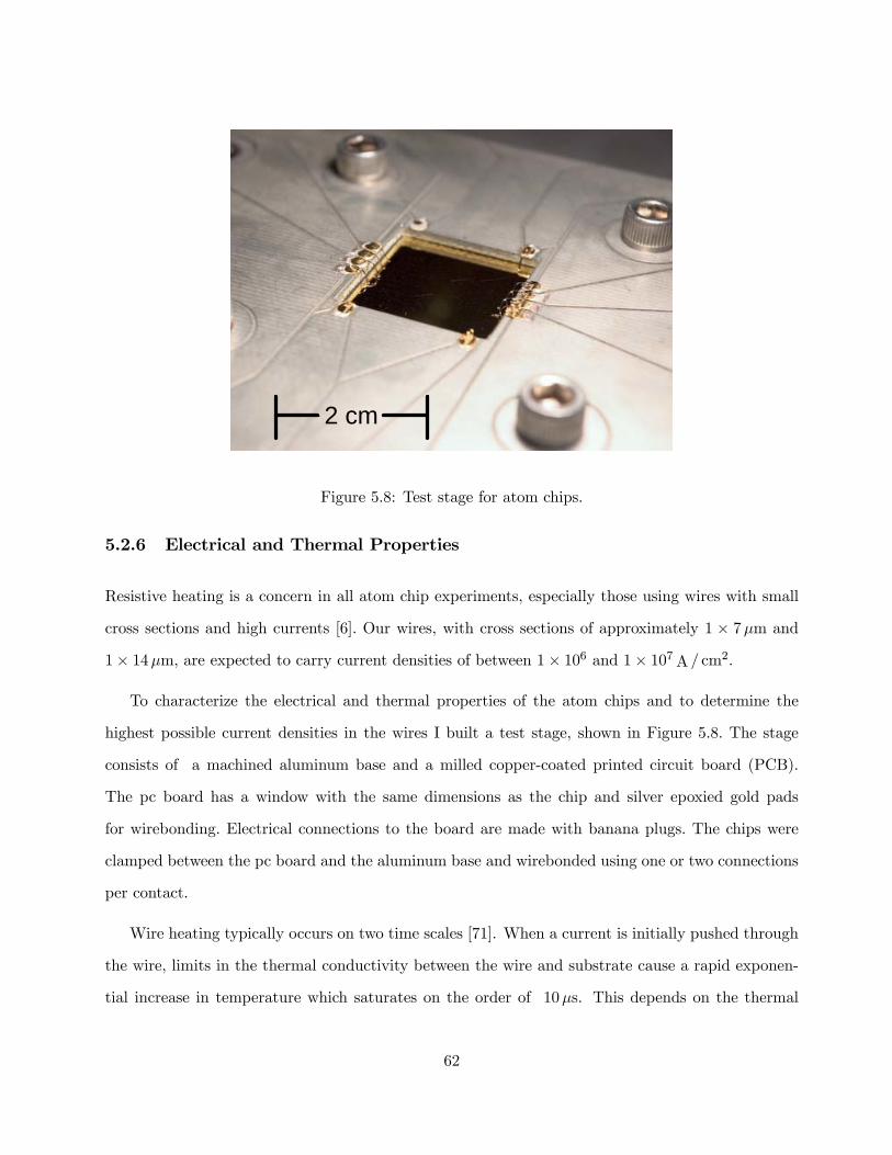
2 cm
Figure 5.8: Test stage for atom chips.
5.2.6 Electrical and Thermal Properties
Resistive heating is a concern in all atom chip experiments, especially those using wires with small
cross sections and high currents [6]. Our wires, with cross sections of approximately 1 × 7μm and
1× 14μm, are expected to carry current densities of between 1× 10⁶ and 1× 10⁷A / cm2.
To characterize the electrical and thermal properties of the atom chips and to determine the
highest possible current densities in the wires I built a test stage, shown in Figure 5.8. The stage
consists of a machined aluminum base and a milled copper-coated printed circuit board (PCB).
The pc board has a window with the same dimensions as the chip and silver epoxied gold pads
for wirebonding. Electrical connections to the board are made with banana plugs. The chips were
clamped between the pc board and the aluminum base and wirebonded using one or two connections
per contact.
Wire heating typically occurs on two time scales [71]. When a current is initially pushed through
the wire, limits in the thermal conductivity between the wire and substrate cause a rapid exponen-
tial increase in temperature which saturates on the order of 10μs. This depends on the thermal
62

conductivity of the substrate or, in our case, the thermal conductivity of the 40 nm SiO2 insulating
layer. The second time scale is a slow heating of the wires while heat is lost to the substrate and to
the chip mount. Groth et al . [71] modelled the slow heating as a logarithmically increasing function
of time.
The following measurements were made on a chip with 1.2μm thick Au wires on a 10-20 nm
thick Cr adhesion layer. The 7μm-wide centre wire and a 14μm-wide U-wire were used. Their room
temperature resistances, R, were 14 and 6.8Ω, respectively. The first test I performed was to measure
the resistive heating, ∆R, of the wires as a function of current. I sent a pulse of constant current
through a wire and measured the voltage drop across it. From the voltage I calculated resistance
and then wire temperature using
∆T =1
α
∆R
R0(5.2)
where α is the temperature coefficient of resistance (0.0034 for Au). The pulse length was 500ms
with a 10 s duty cycle, similar to that to be used in atom chip experiments. Measurements were not
made under vacuum so wire heating was less than it would have been under the UHV conditions of
actual experiment since heat could be lost by convection. To avoid damaging the wires, I imposed
a cut-off when resistance rose by 50%, corresponding to a temperature rise of about 100 C. Figure
5.9 plots the resistance increase due to fast heating as a function of current through the 7μm and
10μm wires. The data points were taken at the end of each current pulse. The increase in resistance
due to slow heating is shown in Figure 5.10.
The maximum current density achieved by the 7μm wire in air was nearly 10×106A / cm2 before
the resistance rose by 50 %, well above what is required. The 14μm wire could easily carry 1A
(6× 10⁶A / cm2) of current before heating became an issue.
To ensure that chips with the Ti/Pd/Au metallizations behave similarly, I repeated the previous
measurements on a chip with 1.4μm thick gold wires on 20 nm Ti/50 nm Pd adhesion and passivation
layers. The room temperature resistances were 18 and 7.8Ω for the 7 and 14μm wires respectively.
The wires could repeatedly handle current densities of 9 × 10⁶A / cm2 (0.6A) and 8 × 10⁶A / cm2
(1.2A) as seen in Figures 5.11 and 5.12. These results more closely match those of Groth et al . [71]
63

0 2 4 6 8 101
1.03
1.06
1.09
1.12
1.15
1.18
Current Density (x10 6 A/cm2)
Rfa
st/R
0
14 μm
7 μm
Figure 5.9: Change in resistance due to fast heating for Cr/Au wires of Chip 1. The solid lines areto aid the eye.
0 2 4 6 8 100
0.05
0.1
0.15
0.2
0.25
0.3
0.35
Current Density (x10 6 A/cm2)
(Rsl
ow-R
fast
/R0
14 μm
7 μm
Figure 5.10: Change in resistance due to slow heating for Cr/Au wires of Chip 1. The solid lines areto aid the eye.
64

0 1 2 3 4 5 6 7 8 91
1.05
1.1
1.15
1.2
Current Density (x10 6 A/cm2)
Rfa
st/R
0
7 μm
14 μm
Figure 5.11: Change in resistance due to fast heating for Ti/Pd/Au wires of Chip 2. The solid linesare to aid the eye.
where the fast heating is independent of wire cross sectional area but the slow heating is higher for
wider wires.
When using the chip in an experiment, all five wires may be required to carry current simulta-
neously. More power is dissipated into the substrate with multiple wires carrying current, leading
to increased substrate heating. Figure 5.13 shows the effect of running current through the five chip
wires on wire resistance compared that of a single wire. Each wire carries the same current density.
Slow heating is increased considerably, setting limits on the maximum currents to around 300mA
for the centre wires and 600mA for the outer U-wires.
To characterize heating on longer timescales I measured the resistance increase as a function of
pulse length. In a typical atom chip experiment the wire would only be carrying current for around
0.5 s, however it is useful to compare the thermal performance of our chip with that of Groth et
al . [71], since our choice in silicon substrate and SiO2 insulator was based on their results. Figure
5.14 shows the increase in resistance of the centre wire as a function of pulse duration for both 500
and 600mA currents. The duty cycle up to measurements of 3 s pulse durations was 10 s and was
65
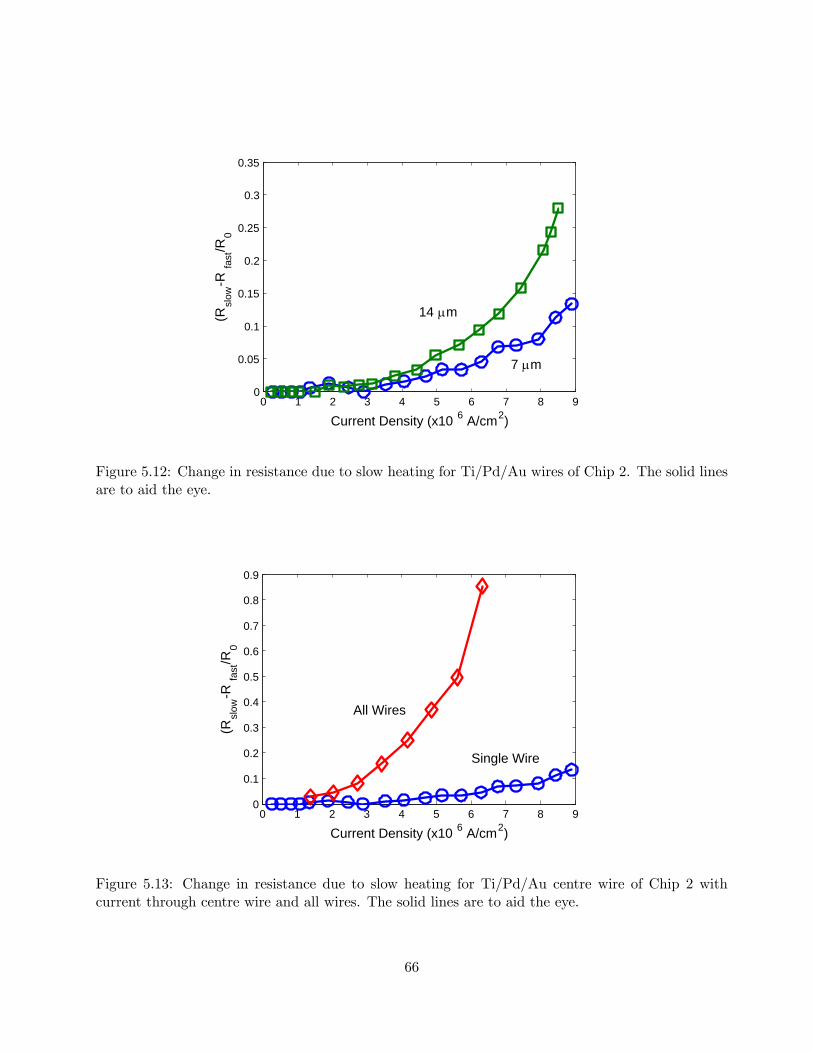
0 1 2 3 4 5 6 7 8 90
0.05
0.1
0.15
0.2
0.25
0.3
0.35
Current Density (x10 6 A/cm2)
(Rsl
ow-R
fast
/R0
14 μm
7 μm
Figure 5.12: Change in resistance due to slow heating for Ti/Pd/Au wires of Chip 2. The solid linesare to aid the eye.
0 1 2 3 4 5 6 7 8 90
0.1
0.2
0.3
0.4
0.5
0.6
0.7
0.8
0.9
Current Density (x10 6 A/cm2)
(Rsl
ow-R
fast
/R0
All Wires
Single Wire
Figure 5.13: Change in resistance due to slow heating for Ti/Pd/Au centre wire of Chip 2 withcurrent through centre wire and all wires. The solid lines are to aid the eye.
66

0 5 10 151
1.1
1.2
1.3
1.4
1.5
Time (s)
R/R
0
600 mA
500 mA
Figure 5.14: Change in resistance as a function of heating time for centre wire of Chip 1. The dashedlines are log fits.
then increased to 20 s for the remainder of the measurements. The slow heating is expected, with
resistance increasing logarithmically with time, as shown in the fit lines in figure 5.14.
Measurements of resistance versus time for the centre wire of a Ti/Pd/Au chip yields different
results than for the Cr/Au chip (see Figure 5.15). The resistance in the wire reaches a maximum
value after a few seconds and remains there for the duration of the pulse. It appears that the
temperature in the wire reaches an equilibrium value at this point. It is unclear at this point why
the heating is different between these two chips, and further measurements are necessary.
5.2.7 Wire Edges and Surface
As mentioned in Section 2.1.3, the roughness of the wire edges can impact the quality of the trapping
potential. Edge corrugations cause the wire current to stray from an axial direction, leading to
inhomogeneous axial magnetic field contributions to the potential. The lift-off process is used for
fabricating the wires to minimize edge roughness.
The edge of a typical Cr/Au wire of the Chip 1 design is shown in Figure 5.16 from the Watlab
67

2 4 6 8 101
1.1
1.2
1.3
1.4
1.5
Time (s)
R/R
0
700 mA
600 mA
500 mA
300 mA
Figure 5.15: Change in resistance of centre wire of Chip 2 as a function of heating time for 300, 500,600, and 700mA.
SEM. The wire edges is smooth, with deviations of < 100 nm in the direction perpendicular to the
wire edge. The overall shape of the edge mimics the edge of the photoresist. The roughness is close
to being limited by the size of the Au grains (∼ 50 nm). Also visible in Figure 5.16 is a faint line of
residue 450 - 500 nm to the left of the wire. This line indicates the point where the lift-off resist had
made contact with the substrate.
The edge roughness of a typical Chip 2 wire is shown at 50, 000× and 10, 000× magnifications
in Figures 5.16 and 5.18. This chip has been submitted to three cures at 350 C, which has had
an annealing effect on the metal (see Section 77). The wire edge features are no longer limited by
the edge of the lift-off resist, but by the larger grain size of the annealed Au. The grain structure
is difficult to see in these SEM images, but is more apparent in the AFM (ThermoMicroscopes
Explorer) scan of Figure 5.19. The grains have grown from the pre-annealed size of 50− 100 nm to
between 3 and 10μm. Despite the enlarged grain size, the edge deviations have only increased to
about 200 nm.
The above images are typical of the observed areas on the chips. However, to properly characterize
68

Figure 5.16: SEM image of a Chip 1 wire edge at 50,000 × magnification.
Figure 5.17: SEM image of a Chip 2 wire edge at 50,000 × magnification.
69

Figure 5.18: SEM image of a Chip 2 wire edge at 10,000 × magnification.
81 nm
0 nm
Figure 5.19: AFM image of surface of a Chip 2 wire.
70

wire edge corrugations, a larger sampling would be required. Schumm et al . [26] overlayed 66 SEM
images to measure the edge roughness of full 2.8mm wire lengths and determine the spectral density
of the fluctuations.
5.3 Planarization
For Chip 2, the next step in the process after fabricating the trapping wires is to obtain a flat,
smooth surface, electrically isolated from the wires, on which the shield layer can be deposited. Of
the planarization methods discussed in Sections 3.4 and 4.4 we decided that using a spin-coated
planarizing dielectric was most feasible. Initially I attempted to develop a process for spin-on glass
with little success (Section 5.3.1). I then switched to polyimide (Section 5.3.2) for planarizing the
final device. Once the polyimide is applied it must be patterned to reveal the bond pads on the wire
layer. The patterning process is illustrated in Figure 5.20.
5.3.1 Spin-on Glass
My first attempts to planarize the trapping wires were with Accuglass T-512B spin-on glass (Hon-
eywell, www.electronicmaterials.com), a methylsiloxane polymer in solvents (methanol, IPA and
acetone). It is a low-κ dielectric, applied in a similar fashion as photoresist but cured at a much
higher temperature (450 C). T-512B is designed with the ability to spin a second layer over the first,
with a maximum thickness of 2μm. The process of applying T-512B is:
1. Dehydration bake wafer at 150 C for 10min
2. Coat entire wafer surface with T-512B using syringe and 0.2μm filter
3. Spin at 2000 RPM for 30 s
4. Hotplate bake 80 C for 60 s, 150 C for 60 s, (250 C for 60 s)
5. Optional: coat second layer by repeating above
T-512B is intended to be cured in a nitrogen-fed furnace since the film is prone to flaking if cured
in the presence of oxygen. The cure cycle for T-512B is:
71
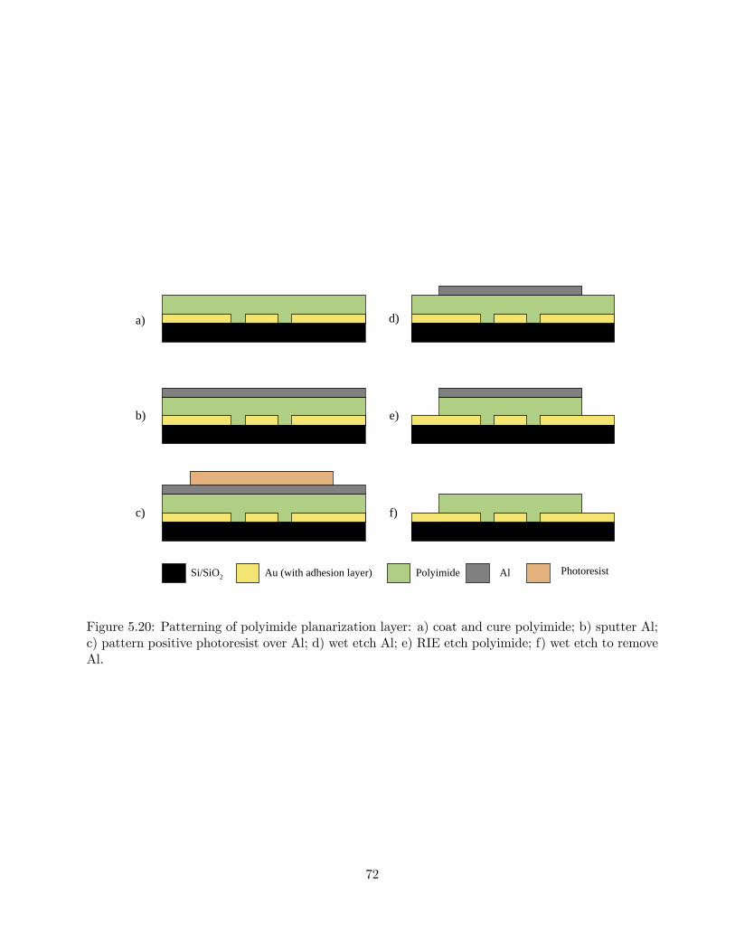
Si/SiO2 Au (with adhesion layer) Polyimide Al Photoresist
a)
b)
c)
d)
e)
f)
Figure 5.20: Patterning of polyimide planarization layer: a) coat and cure polyimide; b) sputter Al;c) pattern positive photoresist over Al; d) wet etch Al; e) RIE etch polyimide; f) wet etch to removeAl.
72

700
-700
0
0 10 20 30
Position (μm)
Hei
ght (
nm)
554 nm
Figure 5.21: Planarization with a single layer of T-512B spin-on glass over 1μm thick Au wires.
1. Load wafer at 250 C
2. Ramp up at 2.5 C /min to 425 C
3. Cure (soak) for 60min
4. Ramp down at 5 C /min to 300 C
5. Unload
I spun and baked the spin-on glass (SOG) at the Watlab facility in a small fume hood. Un-
fortunately, the fume hood was not a clean environment and particle contamination was a serious
problem. At that time, I had no access to a furnace for curing in an inert atmosphere. Instead I cured
the SOG on a non-programmable hotplate (VWR 355, www.vwrcanlab.com), manually ramping the
temperature. After the full cure, many of the SOG films had significant cracking across the entire
wafer. While this occurred on only some of the single-layer films, every two-layer film had cracking.
It was also noticed that the cracking in the films increased over time and that flaking started to
occur. Likely causes of the cracking are poor adhesion between the SOG and the gold, tensile stress
and corrosion due to moisture [87]. Optimized processes are available for achieving stable SOG films,
however these require the deposition of an oxide or nitride over the metal and a cure in an inert
environment, both of which were unavailable when working with SOG.
73

A single layer of SOG T-512B gives a degree of planarization (see Section 3.4) of about 50%, as
measured by the Watlab AFM (Digital Instruments Dimension 3100, www.veeco.com) and plotted
in Figure 5.21. A second coating of SOG should improve the DOP, but I was unable to fabricate a
measurable sample due to the cracking and flaking problems discussed above.
5.3.2 Polyimide
I have used two types of polyimides (Section 4.4) as planarization layers, PI 2611 and PI 2562 (HD
Microsystems, http://www.hdmicrosystems.com). Both are polyamic acids that come dissolved in
N-methyl-2-pyrrolidone (NMP) and have similar application and curing methods. A PI 2611 process
was developed first, as it was available at the CIRFE lab. Coating, curing and etching techniques
were expected to be applicable to either polyimide. It is a low stress material with a low coefficient of
thermal expansion (CTE), intended as an insulator between metal layers in microelectronic devices.
The polymer chains of PI 2611 have a rigid rod backbone, which allows them to lie parallel to
the surface [54]. Unfortunately this polyimide has poor planarity since the rigid polymers do not
easily flow from the metal lines to fill gaps. PI 2562, while thinner, is designed to be a planarizing
intermediate layer.
To increase planarity, additional layers of PI 2611 or PI 2562 can be applied. Subsequent layers
of PI 2611 can only be coated over fully cured films1. Additional coatings of PI 2562 can be applied
either after the pre-cure hotplate back or after a full cure. However, the degree of planarization of
PI 2562 differs between these two methods (Section 5.3.5).
Both polyimides require an adhesion promoter before application. The recommended adhesion
promoters are HD Microsystems VM 651 and VM 652. VM 651 is a concentrate and must first
be diluted in water or methanol/water, while VM 652 comes pre-diluted. I worked with VM 651
originally and found it often left beads of liquid on the chips after spinning, likely due to poor mixing
of VM 651 and water. Therefore, I began using VM 652 which coats with consistent results.1The effect of applying an additional layer over an uncured layer of PI 2611 is shown in Figure 5 in Appendix III.
74

Dehydration Bake Wafer
Spin Coat VM 652 Adhesion Promoter
Bake VM 652
Spin Coat Polyimide
Hotplate Bake
Cure
A
B
Figure 5.22: Application process for PI 2562 and PI 2611. For applying additional layers, A is possiblewith both PI 2562 and PI 2611 and B with PI 2562 only.
Adhesion Promoter Application
HD Microsystems VM 652 adhesion promoter comes pre-diluted, requiring no further modification
before use. I first decant the promoter into a 500 mL Nalgene bottle to minimize the number of
times the large bottle is opened. For each session I fill a 20 mL syringe with promoter, removing any
air bubbles by pointing the syringe upright and slowly applying pressure to the plunger. I dispense
the promoter onto the wafer through a 0.4μm filter. VM 652 has a lifetime in the syringe of just
24 h and so at the end of the session I dispose of the remaining promoter into a waste bottle and
clean the syringe with DI water.
The method for applying VM 652 is:
1. Bake wafer at 150 C for 15-30min for dehydration
2. Coat entire wafer surface with VM 652 and let stand for 20 s
3. Spin at 3000 RPM for 30 s
4. Hotplate bake at 120 C for 30 s
75

Polyimide Application
Polyimides PI 2562 and PI 2611 are bought in 250 mL bottles, with a shelf-life at −18 C of 2 years.
Before opening a bottle it must be warmed to room temperature, usually 5 h after removing from
the freezer. To minimize the number of times the polyimide is thawed I decant it into several 30ml
Nalgene bottles that I store in the freezer. At room temperature PI 2611 can be used for 2 weeks and
PI 2562 for 4 weeks before properties of the polyimide begin to change, primarily due to moisture
absorption.
Polyimide is applied as follows:
1. Centre wafer on vacuum chuck of spinner
2. Slowly pour polyimide onto centre of wafer from Nalgene bottle, enough so that the spun filmcompletely covers wafer
3. Spin 500 rpm for 10 s
4. Spin 3000 rpm for 30 s
5. On hotplate, bake PI 2611 at 90 C for 2min then 150 C for 2min, bake PI 2562 at 120 C for5min
6. Clean spinner with AZ PG Remover
I pour polyimide onto the wafers directly from the small Nalgene bottles. Attempts to use
manual syringes and dispenser syringes failed due to trapped air bubbles. Even if left inverted for
long periods of time, bubbles remained trapped in PI 2611 syringes. As a result, dispensed films had
many pinholes caused by air bubbles.
To spin a uniform coating, the wafer must be centred on the spinner vacuum chuck.
With PI 2562 it is possible to apply an additional layer after the hotplate bake to obtain a thicker
film and to improve planarity. I have applied a second and third layer before curing. This approach
does not work with PI 2611, giving highly non-uniform coatings.
76

Polyimide Cure
Polyimide must be cured after the hotplate bake to completely remove solvents. I cure polyimide in
a nitrogen-fed furnace with a final cure temperature of 350 C. The cure cycle for PI 2611 is:
1. Load at 150 C
2. Ramp to 350 C at 4 C /min
3. Cure for 30min
4. Switch oven off and allow to cool
5. Unload at 150 C
The cure for PI 2562 is:
1. Load at 120 C
2. Ramp to 200 C at 4 C /min
3. Cure for 30min
4. Ramp to 350 C at 2.5 C /min
5. Cure for 60min
6. Switch oven off and allow to cool
7. Unload at 180 C
An unfortunate feature of the furnace is that the ceramic lining sheds particles which fall onto
the polyimide surface during the cure. I have found that these cling to the surface, or occasionally
get embedded in the film during the cure. Blowing the wafers with the N2 gun is insufficient. The
particles on the surface become apparent when coating with another layer of polyimide or photoresist,
causing what appear to be pinholes in the film. Inspection of the features in the microscope reveals
them as irregularly shaped particles embedded in the newly spun film.
Samples cured uncovered result in polyimide films with five to ten defects on the order of a few
hundred microns in diameter scattered randomly over the chip area. In an attempt to eliminate
77
particles from falling onto the polyimide surface, I propped a glass beaker cover over the wafers
during the cure. After removing from the oven, I put the wafers in petri dishes of IPA and placed
them in a low power ultrasonic clean to shake loose any potential particles. This gave inconsistent
results, with some samples being totally free of particles but others not. For the final run of chips,
I set the wafers in a covered petri dish for each polyimide cure. After three coatings and cures, four
out of the five chips had no particles whatsoever in the film and the fifth had just one.
5.3.3 Polyimide Patterning
PI 2611 and 2562 are dry etch polyimides, meaning they can be patterned using plasma etchers such
as RIE, ICP or barrel etchers (see Section 3.5). The patterning process is illustrated in Figure 5.20.
Masking
I have used aluminum and SiO2 as masking materials for polyimide plasma etching. Aluminum
is sputtered using the Intelvac to thicknesses ranging from 0.5 to 2μm. SiO2 is deposited using
the Trion PECVD (TRION Orion II, www.triontech.com). I pattern both using AZ 3312 positive
photoresist and a wet etch in either PAN etch (1:16:1:2 H3PO4:CH3COOH:HNO3:H2O [83]) for Al
or buffered HF (BHF) for SiO2. During the polyimide etch, SiO2 develops pinholes near feature
edges which leads to micro-masking effects (shown in Figure 9 in Appendix III). Therefore, use of
SiO2 was abandoned.
Aluminum was chosen over other metals because of its relative affordability and ease of sputtering
and etching. By using the Intelvac for sputtering the Al, many samples can be coated to the
same thickness simultaneously and quickly, the entire process taking around 1.5 hours. Before Al
deposition, the polyimide samples must go through a dehydration bake at 180 C for 30 to 60min
to remove absorbed water. I clean the samples in IPA and blow them dry to remove any dust that
could cause pinholes in the Al film.
I pattern the aluminum using AZ 3312 positive photoresist. The procedure for patterning the
resist is:
78
1. Coat AZ 3312 photoresist over entire wafer surface using dispenser syringe and 0.45μm filter
2. Spin at 3000 RPM for 30 s
3. Soft bake on vacuum hotplate at 90 C for 60 s
4. Align with mask aligner, matching alignment marks on wafer with those on mask
5. Expose for 12 s
6. Post-exposure bake on vacuum hotplate at 110 C for 60 s
7. Develop in beaker of AZ 300 MIF for 60 s
8. Rinse in beaker of DI water and then under DI water spray gun
9. Dry with N2 gun
10. Inspect for correct alignment and pinholes with microscope
Since photoresist is used to define an etch mask, it is very important that there are no holes
in the resist. I clean the wafer in a petri dish of IPA in an ultrasonic bath and then blow dry to
remove any particles immediately before coating with resist. Another cause of pinholes in photoresist
is air bubbles trapped in the film during dispensing. To minimize this, I hold the dispenser syringe
vertically with the tip pointing up and push slowly on the plunger until the air bubbles are removed.
Before coating the wafer, I dispense the first few drops of resist into a beaker to remove any air
that may have been trapped in the tip. When coating I start at an edge of the wafer and dispense
continuously over the surface in a scanned pattern, being careful to not break the meniscus between
the surface and the syringe tip.
This is the first step in the chip fabrication process that requires precise alignment, since the
etched polyimide layer must be accurately positioned over the wires. The Oriel mask aligner has a
single x-axis and two independent y-axis micrometers that can be used to translate and rotate the
wafer chuck for aligning with the mask. My procedure for aligning is to raise the wafer towards the
mask until contact is reached and then lower the wafer slightly. The minimum distance between
the two objectives of the split field microscope is larger than the size of the wafer, so viewing two
alignment marks simultaneously is not possible. Instead I line up the corresponding alignment marks
of the chip and the mask at one point, and then translate the microscope to a neighbouring alignment
79

mark and adjust the rotation and translation until they line up. Once all four alignment marks are
checked, I raise the wafer into contact with the mask and evacuate the chamber surrounding the
wafer and mask. Occasionally, the wafer will shift slightly at this point and the alignment must be
repeated. If the degree and direction of the shift is consistently repeated, the wafer can be aligned
with a corresponding offset to compensate for the shift. This is an iterative process that improves
a great deal with practice.
I etch the aluminum in PAN etch in a glass beaker at 40 - 45 C. Etch times vary between 0.25
and 1μm /min depending on the temperature. I set the wafer in the PAN etch beaker and gently
swirl it around until the 5 s after the Al is visibly etched away and rinse it in a beaker of DI water. At
this point the photoresist is no longer necessary, so I transfer the wafer into a petri dish of acetone
to remove the resist. I soak it for 5min and transfer it to a petri dish of IPA for another 5min.
ICP/RIE Etch
Polyimide is commonly etched using inductively coupled plasma/reactive ion etch (ICP RIE, see
Section 3.5) systems using O2 or O2/CF4 [88], [89], [90]. I have attempted etches with each of these
gases, as well as O2/SF6, with mixed results. All etches were done using the CIRFE ICP RIE system
(Trion Phantom II, ww.triontech.com) with Reena Al-Dahleh, a PhD student at CIRFE.
Again, we developed recipes for polyimide PI 2611 initially due to availability, but continue to
use the same recipes for PI 2562. As a starting point we used the O2/SF6 polyimide etch recipe
recommended by the manufacturer of the RIE, Trion. This was quickly abandoned, however, as the
etch process was highly non-uniform and left residue on the wafer stage and on the wafer itself (see
Figure 7 in Appendix III).
The most effective etch that we have developed uses pure O2 at low pressure and high ICP power2.
Low pressure increases the mean free path of the accelerated ions which improves the anisotropy of
the etch. The etch recipe is:2O2/CF4 was found to leave considerable residue on the wafer surface, as shown in Figure 8 in Appendix III).
80

Pressure 10 mTorr
ICP Power 500W
RIE Power 25W
O2 Flow 35 sccm3
The procedure for etching using the Trion system begins by first pumping out the chamber
without a sample and tuning the ICP and RIE variable capacitor pairs to minimize the reflected rf
power. This is done by minimizing reflected power with one capacitor in the pair and then minimizing
with the other and repeating back and forth. With the above etch recipe the reflected ICP power
can be brought to between 1 and 10W and the RIE power to between 0 and 1W. Once the tuning
is completed, the chamber is vented and loaded with the sample.
The etch rate for PI 2611 is about 1μm /min and is about 0.85μm /min for PI 2562. While the
bulk of the polyimide is being etched, the plasma has a dull pink glow which fades to a dim grey
once the etch stop (gold and wafer surface) is reached. At this point I etch for an additional 30 s
to remove the remaining polyimide from the edges of the wires where the film was thickest. After
removing the sample from the chamber I inspect it with the microscope to ensure that the polyimide
is fully etched. Once etching is complete, I remove the Al mask in PAN etch.
When etching polyimide samples consecutively, the etch rate decreases with each run. This is
likely due to a polyimide residue building up on the chamber walls and, indeed, running a plasma
clean restores the etch rate. The clean parameters are:
Pressure 50 mTorr
ICP Power 250W
RIE Power 62W
O2 Flow 45 sccm
SF6 Flow 5 sccm
The etch process often leaves a thin layer of residue over the newly exposed surface. This residue is
likely a mixture of polyimide and a small amount of Al that sputtered in the plasma and redeposited
over the wafer. Fortunately, the PAN etch used to remove the Al etch mask also removes this residue.3Standard cubic centimetres per minute
81

Figure 5.23: SEM image of edge of polyimide planarization layer with Al etch mask.
Despite the low pressure of the etch it is not fully anisotropic. The top of the polyimide sidewall
undercuts by about 2μm although the base has nearly no undercut4. This degree of undercut is
within the allowed tolerances, as the polyimide layer spans 20μm past each edge of the shield layer.
The roughness of the sidewalls mirrors that of the aluminum etch mask. As an insulating layer
between the wires and shield, smooth sidewalls are not required. For applications where the sidewall
smoothness is important, the aluminum edge roughness can be minimized by patterning with lift-off
as opposed to wet etching. Figure 5.23 shows an etched polyimide layer (with aluminum etch mask
intact) at the edge of a wire.
5.3.4 Pinholes
The main drawback of the method of patterning the polyimide is holes etched in the polyimide film.
I initially noticed this when I deposited and patterned the first shield layers over chips. Each sample
had a short between the shield and at least one of the wires. The possible causes are: holes in the
polyimide film after spinning and curing; a hole in the Cr mask; pinholes in the photoresist used to4Overetching will cause undercut, as shown in Figure 10 in Appendix III.
82
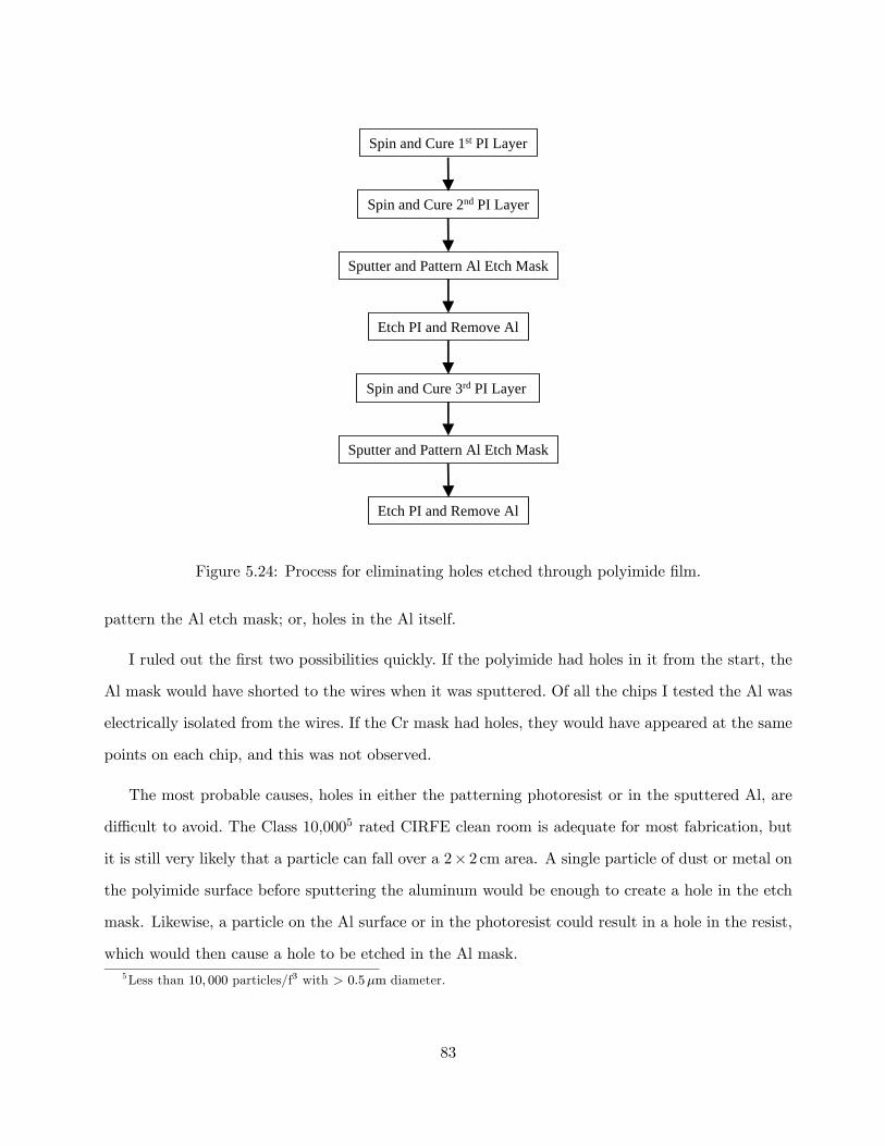
Spin and Cure 1st PI Layer
Spin and Cure 2nd PI Layer
Sputter and Pattern Al Etch Mask
Etch PI and Remove Al
Spin and Cure 3rd PI Layer
Sputter and Pattern Al Etch Mask
Etch PI and Remove Al
Figure 5.24: Process for eliminating holes etched through polyimide film.
pattern the Al etch mask; or, holes in the Al itself.
I ruled out the first two possibilities quickly. If the polyimide had holes in it from the start, the
Al mask would have shorted to the wires when it was sputtered. Of all the chips I tested the Al was
electrically isolated from the wires. If the Cr mask had holes, they would have appeared at the same
points on each chip, and this was not observed.
The most probable causes, holes in either the patterning photoresist or in the sputtered Al, are
difficult to avoid. The Class 10,0005 rated CIRFE clean room is adequate for most fabrication, but
it is still very likely that a particle can fall over a 2× 2 cm area. A single particle of dust or metal on
the polyimide surface before sputtering the aluminum would be enough to create a hole in the etch
mask. Likewise, a particle on the Al surface or in the photoresist could result in a hole in the resist,
which would then cause a hole to be etched in the Al mask.5Less than 10, 000 particles/f3 with > 0.5μm diameter.
83

Figure 5.25: Cross section of three layers of polyimide. Etching the first two layers and then coatingand etching the third layer ensures no holes will span the full depth of the polyimide.
To get past the limitations of the clean room and to insure that there could be no holes in the
final patterned polyimide, I altered the original process (Figure 5.24). I coat the first two layers with
a cure between each and then RIE etch them using the aluminum as a mask. I then spin and cure
the third polyimide layer. Any holes that may have been etched in the first two layers are partially
filled by the third. I etch the top layer with the same process as the lower two, with a shorter
etch time due to the thinner film. If a new hole is etched in this layer, it will not reach the wires
below (Figure 5.25). The drawback of this method is that it adds an extra aluminum deposition,
photoresist patterning, aluminum etch and polyimide etch. It also has an additional alignment step
when patterning the resist.
.
5.3.5 Degree of Planarization
The degree of planarization of polyimide (DOP, Section 3.4) is dependent on the type of polyimide,
the spin speed at which it is coated, the number of layers and whether the film is fully cured between
successive coatings. It also depends on the topography of the underlying surface, especially the widths
of features and gaps between them.
A single layer of PI 2611, spun at 4000 RPM (5μm) gives a DOP of 20-30% at the centre wire
and a 0% DOP at the larger gaps. A single layer of PI 2562, however, spun at 3000 RPM for 1.5μm
gives a 40% DOP over the centre wire. Already, the planarization abilities of PI 2562 are apparent,
84

Figure 5.26: SEM image showing etched-back polyimide film over centre trap wires to demonstrateplanarization.
since it has a better DOP with a thinner layer. Coating with two layers of PI 2562 before curing
increases DOP to 50-60%. In contrast applying a layer of PI 2562 over a fully-cured single layer gives
a DOP of 70-80%. Planarization is improved further to 80-90% by applying a third layer.
The final chips were planarized using three layers of PI 2562, with a full cure between each layer.
As a demonstration of the planarization, I removed a region of polyimide over the trapping wires
using an RIE etch, as shown in Figures 5.26 and 5.27. Wire height is 1.5μm. Figure 5.28 shows
a Dektak scan (Section 3.9) over the five wires. Around the centre wire, the peak-to-peak height
variation of the polyimide surface is 240 nm. With the 1.5μm thick wires underneath, the DOP is
84%.
5.4 Shield Layer
The shield layer is fabricated by depositing a 20 nm chromium adhesion layer and then a 100 nm gold
layer over the polyimide and patterning with lift-off photolithography. Since the quality of the metal
85

Figure 5.27: SEM image showing etched-back polyimide film over centre trap wires to demonstrateplanarization.
Position [μm]
Hei
ght [
nm]
Figure 5.28: Dektak profilometer scan of polyimide surface over five centre wires. Polyimide wascoated in three layers with full cure between each.
86

film is even more important than that of the wires, the deposition rate must be well controlled.
I begin the process by cleaning the polyimide-coated chips with low power (Power setting of 2)
ultrasonic in a petri dish of pure IPA for 1min. I then submit the chips to a dehydration bake
at 180 C for 30 to 60min in the furnace in a covered petri dish. The lift-off photoresist (AZ 2035
nLOF) is spun at 2000 RPM. This would normally be thicker than necessary for lift-off with such a
thin film, however the resist must be continuous over the 3-4.5μm step of the etched polyimide.
The mask for the shield layer is recessed 20μm from the edges of the polyimide layer. The
alignment step in the mask aligner is the most crucial alignment of the chip fabrication process since
the deposited shield must not spill over the edge of the polyimide and short to the wires. I use the
alignment marks on the wafer to position the mask properly over the polyimide. To ensure that
alignment is perfect I scan the split field microscope along the four edges of the polyimide and make
any necessary adjustments with the translation and rotation micrometers.
The exposure is made in contact mode for 12 s. Bake and develop times are the same as for the
wires (Section 5.4). Once the resist is patterned I inspect the chips with a microscope, paying very
close attention for flaws in the resist in the area of the polyimide edge. Again, cleanliness of the
mask is crucial to avoid defects in the resist and it must be cleaned in an RCA solution before every
patterning session.
I deposit the shield layer in the Edwards evaporator in much the same way as the Cr/Au wires,
with only the deposition rate and thickness changed. I ramp the Cr-coated tungsten rod at 10A / s
and deposit at a rate of 12Hz / s until ∆f is 500Hz for a thickness of 10 to 20 nm. After switching off
the current in the Cr charge I let the system cool for 10min. For the gold, I ramp to 70A at 5A / s
with the shutter closed and then hold for 2min with the shutter open enough to expose the crystal
oscillator. I adjust the current slightly until the rate recorded by the crystal oscillator is between 80
and 100Hz / s (8-10Å / s) and then open the shutter.
Lift-off is done in a beaker of warm (30 C) acetone on a hotplate. To avoid metal particles
sticking to the shield surface I set the wafer holder in the beaker with the wafer facing down so that
areas of metal film that separate fall away from the surface. Occasionally I agitate the wafer but I
87

Trapping wire
Shield
Polyimide
Silicon
100 nm
20 μm
4.5 μm
Figure 5.29: SEM image of edge of shield and polyimide layers of Chip 2.
do this gently near the surface of the acetone to not stir up the metal sitting at the bottom of the
beaker. Once the metal is fully lifted off I remove the wafer holder from the acetone and quickly
rinse with pure acetone. I set the chip in a petri dish of IPA for 5min and then blow dry. To remove
any photoresist residue I immerse the chip in AZ Kwik Strip at 60 C for 30min and then rinse in
DI water. I do not subject the shielded chip to ultrasonic cleaning, since the adhesion of the Cr/Au
is not sufficient to withstand it, as shown in Figure 11 in Appendix III. Once the lift-off is completed
I inspect the chip a final time with the microscope and check for shorts between the shield and the
wires. A SEM image of a completed chip is shown in Figure 5.29). A photograph of a fully fabricated
Chip 2 is shown in Figure 5.30.
To connect the shield to the ground pads (G1 and G2, see Section 4.2) on the wire layer, I apply a
small spot of electrically conducting silver-filled epoxy (Epotek H77, www.epotek.com) with a needle
and cure for 60min at 90 C. The epoxy is UHV compatible and does not block optical access to
the chip (Figure 5.31).
88

1 cm
Figure 5.30: Image of a fabricated Chip 2 with patterned polyimide and shield layer. This is priorto dicing and wirebonding (see Section 5.5).
Figure 5.31: SEM image of silver-filled Epotek H77 epoxy used to connect shield layer to groundpads.
89

Figure 5.32: SEM images of thermally deposited Au (with Cr adhesion layer) over PI 2562. Filmthickness (from left to right): 50, 100, 200, 900, 1400 nm.
5.4.1 Grain Size and Roughness
Initially we chose a thickness of 100 nm for the gold shield layer to keep grain size and surface
roughness low. To see how the grain size and roughness of the gold depend on film thickness I
prepared a sample with thicknesses ranging from 50 to 1400 nm. The substrate was a Si/SiO2 wafer
with a cured PI 2562 layer and strips of Kapton tape as markers to separate each region. I performed
the deposition in the Edwards evaporator, starting with a 10-20 nm Cr adhesion layer. I used the
shutter to mask off areas of the sample, using the tape as a guide for placing the shutter’s shadow.
I first deposited 50 nm across the full sample, then set the shutter to mask the 50 nm region. Once
100 nm was reached, I blocked off the 100 nm region, and so on. The final thicknesses, as measured
with the Dektak, were 50, 100, 200, 900, 1400 nm. The Dektak is calibrated to within +/- 15 nm.
Figure 5.32 shows SEM images of the five thickness regions of the sample. To determine average
grain size I used a counting method. I sampled three smaller areas of each image (~400 × 400 nm)
90
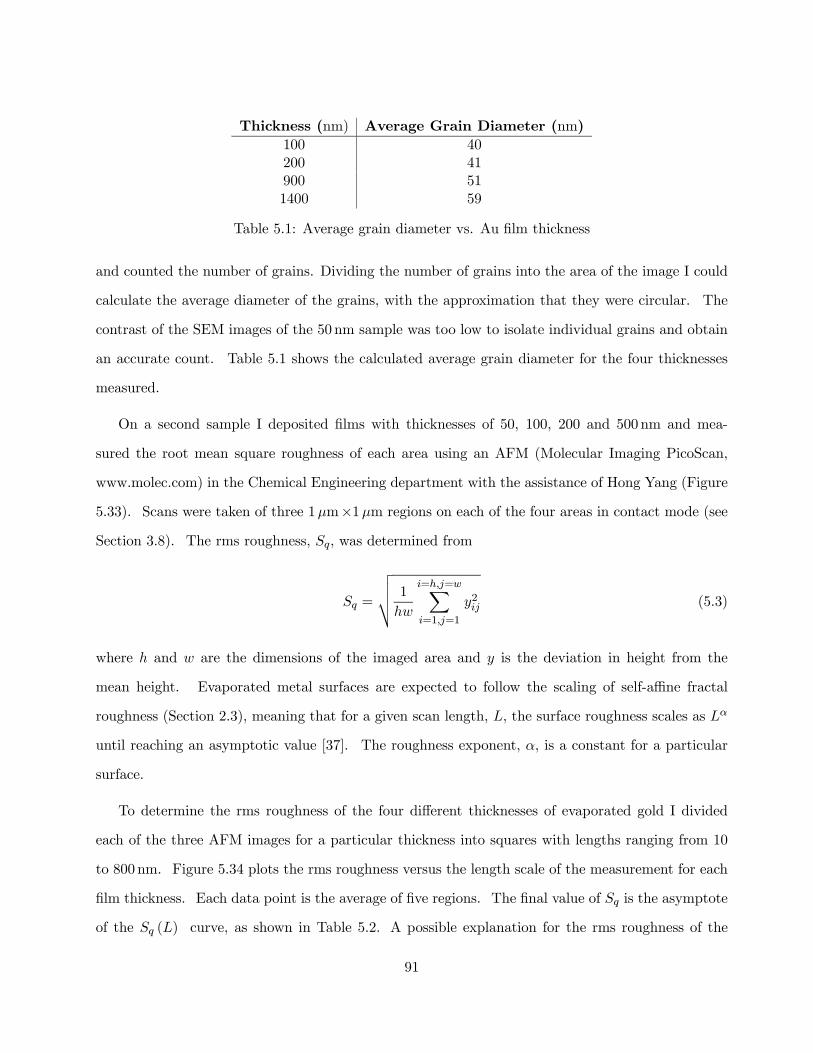
Thickness (nm) Average Grain Diameter (nm)100 40200 41900 511400 59
Table 5.1: Average grain diameter vs. Au film thickness
and counted the number of grains. Dividing the number of grains into the area of the image I could
calculate the average diameter of the grains, with the approximation that they were circular. The
contrast of the SEM images of the 50 nm sample was too low to isolate individual grains and obtain
an accurate count. Table 5.1 shows the calculated average grain diameter for the four thicknesses
measured.
On a second sample I deposited films with thicknesses of 50, 100, 200 and 500 nm and mea-
sured the root mean square roughness of each area using an AFM (Molecular Imaging PicoScan,
www.molec.com) in the Chemical Engineering department with the assistance of Hong Yang (Figure
5.33). Scans were taken of three 1μm×1μm regions on each of the four areas in contact mode (see
Section 3.8). The rms roughness, Sq, was determined from
Sq =
vuut 1
hw
i=h,j=wXi=1,j=1
y2ij (5.3)
where h and w are the dimensions of the imaged area and y is the deviation in height from the
mean height. Evaporated metal surfaces are expected to follow the scaling of self-affine fractal
roughness (Section 2.3), meaning that for a given scan length, L, the surface roughness scales as Lα
until reaching an asymptotic value [37]. The roughness exponent, α, is a constant for a particular
surface.
To determine the rms roughness of the four different thicknesses of evaporated gold I divided
each of the three AFM images for a particular thickness into squares with lengths ranging from 10
to 800 nm. Figure 5.34 plots the rms roughness versus the length scale of the measurement for each
film thickness. Each data point is the average of five regions. The final value of Sq is the asymptote
of the Sq (L) curve, as shown in Table 5.2. A possible explanation for the rms roughness of the
91

Topography Deflection
50 nm
100 nm
200 nm
500 nm
Figure 5.33: AFM scans of Au films on polyimide with thicknesses of 50, 100, 200, and 500 nm.Deflection images are derivative-based to enhance appearance of grain boundaries.
92
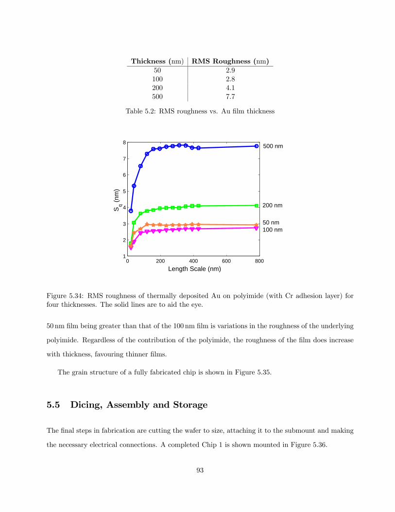
Thickness (nm) RMS Roughness (nm)50 2.9100 2.8200 4.1500 7.7
Table 5.2: RMS roughness vs. Au film thickness
0 200 400 600 8001
2
3
4
5
6
7
8
Length Scale (nm)
Sq (n
m)
500 nm
200 nm
50 nm100 nm
Figure 5.34: RMS roughness of thermally deposited Au on polyimide (with Cr adhesion layer) forfour thicknesses. The solid lines are to aid the eye.
50 nm film being greater than that of the 100 nm film is variations in the roughness of the underlying
polyimide. Regardless of the contribution of the polyimide, the roughness of the film does increase
with thickness, favouring thinner films.
The grain structure of a fully fabricated chip is shown in Figure 5.35.
5.5 Dicing, Assembly and Storage
The final steps in fabrication are cutting the wafer to size, attaching it to the submount and making
the necessary electrical connections. A completed Chip 1 is shown mounted in Figure 5.36.
93

Figure 5.35: SEM image of 100 nm Au layer on polyimide (with Cr adhesion layer).
5.5.1 Dicing
Once the chip fabrication is complete, the device must be cut from the wafer. A crude method is to
use a ruler and diamond scribe to score around the perimeter of the chip. Applying a slight pressure
is enough to cleave the wafer. I have used this technique on unimportant chips only, since the risk of
making an imperfect cleave or scratching the chip is too great.
The completed chips were cut using a dicing saw by Roger Grant in the G2N facility. The saw
uses a computer controlled metal blade to cut part way or fully through the wafer and a stream of
water to rinse away particles. Wafers are held in place by an adhesive pad which sits on a vacuum
chuck. To protect the chips from the freed particles and water, I first coat them with a layer of AZ
3312 resist followed by a 90 C soft bake for 60 s. The photoresist layer is easily removed in acetone
and IPA after dicing. The risk of contaminating the chip surface with photoresist residue is minimal,
since the resist is not cured.
The wafers are squared using a rotation stage and a split field microscope to align a straight edge
on the chip in each of the two images. Since the diced edge is prone to chipping, the blade is offset
94

by about 50μm from the edge of the pattern. The final cut dimensions of the wafers are 2.023 -
2.028 cm square.
5.5.2 Mounting
The chip is mounted to a Macor block that holds the macroscopic U- and Z-wires (see Section 4.1). I
attach the chip to the Macor using Epotek 353ND epoxy (www.epotek.com, P/N AVETZ00001Q8).
I first spread a thin layer of epoxy over the surface of the submount and then very carefully position
the chip. To ensure good contact between the chip and submount, I place a weight on the chip
which touches the four corners only. The epoxy is cured at 120 C.
5.5.3 Wirebonding
The Macor block also holds Au wires that are bent and hammered flat to form bond pads for
connecting to the chip wires. I make electrical connections (see Section 3.6) between the chip and
the pads on the submount with gold ribbon using the K&S Model 4523 ultrasonic wedge bonder
(www.kns.com). A single ribbon, 25 × 250μm, is sufficient to carry the required currents, however
I use a redundant ribbon for each wire. Not only does this minimize the current passing through a
ribbon, it adds security in case a ribbon breaks or a bond becomes unstuck. I use wedges tipped
with a ceramic-metal alloy from Gaiser Tool Co. (www.gaisertool.com, P/N: 4645R-1-10-3.0-3/4-
CG-BKCER) which have a roughened bond foot for better power delivery. Before use, I ultrasonically
clean the wedge in a beaker of acetone.
Before bonding I heat the structure to 150 C using the temperature-controlled stage and wait
for an hour. I make the first bond on the chip and the second bond on the submount. By adjusting
‘Loop Height’, ‘Kink Height’ and ‘Stepback’ I shape the wire so that it is near horizontal after the
first bond. This maximizes the optical access for imaging the trap. Bond settings vary between each
session since the pad temperature, tip cleanliness and other factors are not constant.
To minimize the chance of a wire being pulled from a pad, I apply a drop of silver-filled epoxy
(Epotek H77, www.epotek.com) over each bond and cure at 90 C for 60min.
95

Figure 5.36: Chip 1 mounted to Macor block and wirebonded to Au leads.
Figure 5.36 shows a completed Chip 1 mounted to the Macor block and wirebonded to the Au
leads.
5.5.4 Storage
Over time polyimide absorbs water, requiring storage in a dry environment. An dry environment is
also necessary to minimize the growth of organics on the chip surface. I store the chips in re-sealable
freezer bags. The chips sit in Gel-Boxes (Gel-Pak, P/N AD-23CAS-00-X0 and X4, www.gelpak.com)
cases with holes drilled in the tops. To ensure a dry environment, I make small pouches out of clean
room wipes filled with desiccant pellets. I place the chips and desiccant pouches in the freezer bags
and evacuate them using a vacuum cleaner and thin hose. I then backfill with nitrogen, evacuate
and repeat twice.
96

Chapter 6
Summary and Outlook
I have fabricated atom chips of two designs. Chip 1 is for developing magnetic trapping techniques
and preliminary Rydberg atom experiments. The multi-layer Chip 2 is for Rydberg atom-metal
surface interaction studies. Chip 1 uses five parallel current-carrying wires (1.2μm thick Au over a
12− 20 nm Cr adhesion layer), which were grown by thermal deposition and patterned using lift-off
photolithography. The wires were fabricated on a 500μm thick Si wafer with 40 nm thermal oxide
insulating layer. The chips with the Chip 2 design were patterned with the same method as Chip
1, but with a 20 nm Ti adhesion layer instead of Cr, and a 50 nm Pd buffer layer to eliminate the
diffusion of Ti into the Au during subsequent thermal processing. Diffusion effects were measured
in chips with Cr/Au, Ti/Au, Cr/Pd/Au and Ti/Pd/Au metallizations. After three heating cycles
with a maximum temperature of 350 C, the resistance of the wires rose by 120 %, 5 %, 55 %, and
−1 % respectively. Wire heating resulting from high current densities was measured for both chip
designs. Heating for the Cr/Au and Ti/Pd/Au metallizations was found to be comparable to that
measured by Groth et al . [71], and the wires were found to be capable of the current densities that
will be required during the experiment. Wire edge roughness was within 100 nm for Chip 1 and
within 200 nm for Chip 2.
Chip 2 chips were planarized using three layers of polyimide PI 2562 with a full cure after each
layer application. Polyimide was etched using RIE with a sputtered Al etch mask. To avoid etching
97

pinholes through the polyimide, the polyimide was patterned in two stages: once after applying the
first two layers and again after the third. A total thickness of 3.3μm gave a degree of planarization
of 85 %.
Chip 2 uses an Au electrostatic shield layer above the polyimide to isolate the Rydberg atoms
from electric fields caused by potential differences between the trapping wires. This layer is also a
reflective surface for the laser cooling beams and the surface with which the Rydberg atoms interact.
The shield was fabricated by thermal deposition and lift-off photolithography. The Au grains of the
shield were 40 nm in diameter, as measured with SEM images.
The use of polyimide as a planarizing layer, although ultimately successful, is problematic. The
method of eliminating pinholes is time consuming and inelegant as a microfabrication process. A
photodefinable benzo-cyclo-butene (BCB, see Section 3.4) may be a better choice as a planariza-
tion material, since it can be patterned without RIE. This would avoid the need for intermediate
photoresist and Al masking layers which are prone to holes from dust and air bubbles.
The shield layer of Chip 2 is suitable for preliminary work with Rydberg atoms, but the patch
fields due to the polycrystalline surface will likely limit the types of experiments that can be per-
formed. A surface with a single crystal orientation is expected to minimize the patch potentials by
eliminating grains. Single crystal Au surfaces are commonly grown on ultra-flat template substrates
such as mica, glass and photoresist [91]. Ultra-smooth, single crystal surfaces can be attained by
mounting the backside of the grown Au film to a substrate and peeling off the template [77], [78].
This technique could be incorporated into atom chip fabrication to give a single crystal shield layer
by fabricating the chip in a reverse order on a mica or float glass substrate. Figure 6.1 outlines a
possible “reverse fabrication” method.
Recently, work has been done in our group using ac fields on Rydberg atoms in a MOT [92].
The ac Stark shift is used to tune electric dipole-dipole interactions between atoms into resonance,
which can significantly enhance their interactions. This is accomplished using a macroscopic external
rf source. Fabricating electrodes or waveguides on the chip itself gives the ability to create highly
localized fields, possibly with gradients on the scale of the Rydberg atoms themselves. Treutlein et
98

Mica or Float Glass Au Dielectric Si/SiO2Epoxy
a)
b)
c)
d)
e)
f)
f)
Figure 6.1: “Reverse Fabrication” method to attain a single crystal Au shield layer: a) deposit Auon mica or float glass substrate without adhesion layer; b) coat with a dielectric (polyimide, SiO2);c) pattern Au wires over dielectric; d) epoxy to mounting substrate; e) peel off mica/float glass; f)pattern Au and dielectric to reveal bond pads.
99
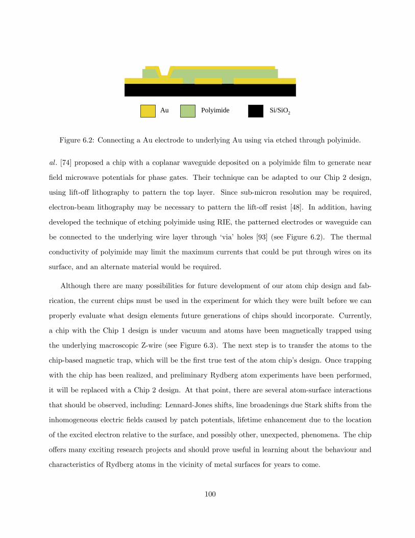
Au Polyimide Si/SiO2
Figure 6.2: Connecting a Au electrode to underlying Au using via etched through polyimide.
al . [74] proposed a chip with a coplanar waveguide deposited on a polyimide film to generate near
field microwave potentials for phase gates. Their technique can be adapted to our Chip 2 design,
using lift-off lithography to pattern the top layer. Since sub-micron resolution may be required,
electron-beam lithography may be necessary to pattern the lift-off resist [48]. In addition, having
developed the technique of etching polyimide using RIE, the patterned electrodes or waveguide can
be connected to the underlying wire layer through ‘via’ holes [93] (see Figure 6.2). The thermal
conductivity of polyimide may limit the maximum currents that could be put through wires on its
surface, and an alternate material would be required.
Although there are many possibilities for future development of our atom chip design and fab-
rication, the current chips must be used in the experiment for which they were built before we can
properly evaluate what design elements future generations of chips should incorporate. Currently,
a chip with the Chip 1 design is under vacuum and atoms have been magnetically trapped using
the underlying macroscopic Z-wire (see Figure 6.3). The next step is to transfer the atoms to the
chip-based magnetic trap, which will be the first true test of the atom chip’s design. Once trapping
with the chip has been realized, and preliminary Rydberg atom experiments have been performed,
it will be replaced with a Chip 2 design. At that point, there are several atom-surface interactions
that should be observed, including: Lennard-Jones shifts, line broadenings due Stark shifts from the
inhomogeneous electric fields caused by patch potentials, lifetime enhancement due to the location
of the excited electron relative to the surface, and possibly other, unexpected, phenomena. The chip
offers many exciting research projects and should prove useful in learning about the behaviour and
characteristics of Rydberg atoms in the vicinity of metal surfaces for years to come.
100

5 mm
Figure 6.3: Absorption image of 87Rb atoms magnetically trapped with macroscopic Z-wire andexternal field coils (provided by Jeff Carter).
101

Appendix I. Process Workflow
This appendix gives an overview of the fabrication steps required for Chip 1 and Chip 2, including
the time required for each step and the relevant section in this thesis. The differences between
ideal and typical times are often due booking equipment efficiently so that it is available when
required. Typical process times also include common errors that are made in photoresist patterning
and polyimide application.
Chip 1
Chip Layer Process Step Time (Ideal/Typical) Relevant Section
Substrate Cleave into quadrants 10min /10min 5.1
RCA clean 60min /60min 5.1
Trapping Wires RCA clean mask 60min /60min 5.2.1
Pattern AZ 2035 nLOF 30min /90min 5.2.2
Deposit Cr/Au 4 h /5 h 5.2.3
Lift-off 30min /90min 5.2.4
Packaging Dice wafer 30min /60min 5.5.1
Epoxy to submount 120min /120min 5.5.2
Wirebond 90min /120min 5.5.3
102

Chip 2
Chip Layer Process Step Time (Ideal/Typical) Relevant Section
Substrate Cleave into quadrants 10min /10min 5.1
RCA clean 60min /60min 5.1
Trapping Wires RCA clean mask 60min /60min 5.2.1
Pattern AZ 2035 nLOF 30min /90min 5.2.2
Deposit Ti/Pd/Au 5 h /6 h 5.2.3
Lift-off 30min /90min 5.2.4
Polyimide Dehydration bake 60min /60min 5.3.2
Apply VM 652 10min /30min 5.3.2
Apply PI 2562 30min /60min 5.3.2
Cure polyimide 4 h /4 h 5.3.2
Apply second layer 5 h /6 h 5.3.2
Sputter Al etch mask 2 h /2 h 5.3.3
Pattern AZ 3312 30min /60min 5.3.3
PAN etch Al 5min /40min 5.3.3
RIE/ICP etch PI 30min /120min 5.3.3
PAN etch to remove Al 5min /40min 5.3.3
Apply/pattern third layer 8 h /12 h 5.3.2 - 5.3.3
Shield Layer Clean and bake wafer 60min /60min 5.4
Pattern AZ 2035 nLOF 30min /90min 5.2.2
Deposit Cr/Au 4 h /4.5 h 5.2.3
Lift-off 30min /90min 5.4
Connect to ground pads 90min /90min 5.4
Packaging Dice wafer 30min /60min 5.5.1
Epoxy to submount 120min /120min 5.5.2
Wirebond 90min /120min 5.5.3
103

Appendix II. Fabricated Chips
This appendix describes the characteristics of the five chips fabricated with the Chip 2 design.
Chip Wire Thickness Notes
(μm)
Feb14_07C 1 Extra cleaning of shield layer (Kwik Strip at 70 C) was
required due to photoresist residue
Mar13_07A 1.2
Mar13_07B 1
Mar15_07B 1.4 Lift-off photoresist began to peel during Au wire deposition,
slight shoulder at base of wire
Mar15_07D 1.5 Lift-off photoresist began to peel during Au wire deposition,
slight shoulder at base of wire
104

Appendix III. Processing Errors
This appendix contains images and explanations of errors that have occurred throughout the devel-
opment of the atom chip fabrication process. Many aspects of fabrication are learned through trial
and error, including photoresist developing and film etching parameters.
Figure 1: Microscope image of patterned lift-off photoresist (Futurrex NR1-3000PY). Dirty chemicalsand improper rinsing and drying lead to contaminants over the substrate surface. This will hinderthe adhesion of subsequent layers.
105

Figure 2: Microscope image of underdeveloped lift-off photoresist (Futurrex NR1-3000PY). The resistis continuous between the wires.
Figure 3: Microscope image of a patch of Au shorting two wires. Defects in the mask or contaminantson the mask surface translate to the patterned films.
106

Figure 4: Microscope image of residue clinging to wire edges. Photoresist residue or thin metal filmsthat may have coated the resist sidewalls must be removed using low power ultrasonic cleaning.
Figure 5: Microscope image of the surface of polyimide PI 2611 after coating with a second layerbefore curing the first layer. Unlike PI 2562, PI 2611 must be fully cured before applying additionallayers.
107

Figure 6: SEM image of PI 2562 after etching in KOH (with Al etch mask). Polyimide can bedissoved in KOH, however etching is not uniform. The film softens beneath the etch mask, causingconsiderable undercut or peeling of large areas. The etched film leaves a residue that is difficult toremove.
Figure 7: Photograph of residue left on the plate of the Trion RIE/ICP after etching polyimide PI2611 with SF6 and O2. This residue was extremelly difficult to remove and did not appear withCF4/O2 and pure O2 recipies.
108

Figure 8: SEM image of the residue left from RIE/ICP etching PI 2611 in O2/CF4. This etch recipeleft considerably more residue than a pure O2 etch.
Figure 9: SEM image of a polyimide PI 2611 film etched in O2 using a SiO2 etch mask. During theetch, pinholes developed in the SiO2, causing a highly undercut film with rough edges. An Al etchmask consitently gives smooth edges with less undercut.
109

Figure 10: SEM image of a RIE/ICP etched polyimide PI 2611 film using an Al etch mask. Over-etching a polyimide film gives a high degree of undercut beneath the Al etch mask.
Figure 11: Microscope image of a Cr/Au film peeling from a polyimide surface after being submittedto an ultrasonic clean. The adhesion between Cr/Au and PI 2562 is sufficient for processing, howeverultrasonic cleaning should be avoided.
110

Figure 12: SEM image of a scratch through a polyimide PI 2562 and Cr/Au film.
111

Appendix IV. List of Acronyms
Acronym Full Name First Appearance
a-SiDIC Amorphous Silicon Devices and Integrated Circuits Group 5
AFM Atomic Force Microscope 3.8
BCB Benzo-Cyclo-Butene 3.4
BEC Bose-Einstein Condensate 1
BHF Buffered Hydrofluoric Acid 5.3.3
CIRFE Centre for Integrated RF Engineering 5
CMP Chemical-Mechanical Planarization 3.4
DI Deionized 5.1
DOP Degree of Planarization 3.4
FIB Focussed Ion Beam 4.3.3
G2N Giga-to-Nanoelectronics Centre 3.7
ICP Inductively Coupled Plasma 3.5
IPA Isopropanol 5.2.4
MCP Micro Channel Plate 4.1
MMOT Mirror-MOT 4.1
MOT Magneto-Optical Trap 2.1.1
PAN Phosphoric-Acetic-Nitric Acid 5.3.3
112
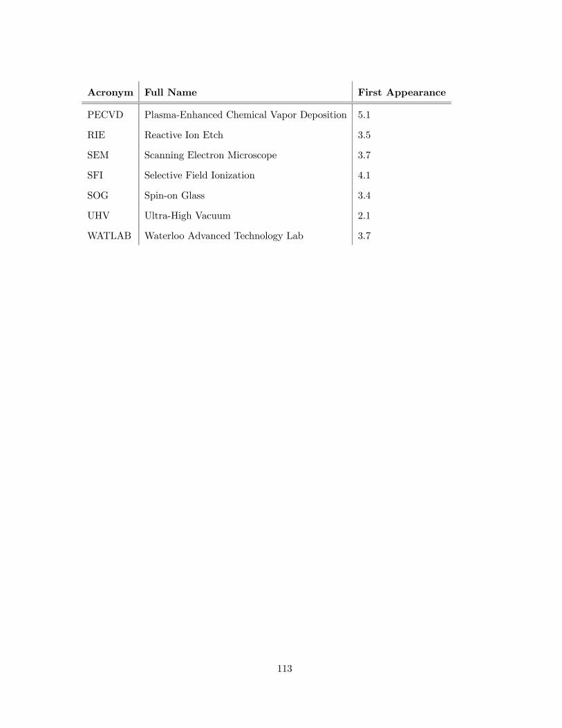
Acronym Full Name First Appearance
PECVD Plasma-Enhanced Chemical Vapor Deposition 5.1
RIE Reactive Ion Etch 3.5
SEM Scanning Electron Microscope 3.7
SFI Selective Field Ionization 4.1
SOG Spin-on Glass 3.4
UHV Ultra-High Vacuum 2.1
WATLAB Waterloo Advanced Technology Lab 3.7
113
Bibliography
[1] Thomas F. Gallagher. Rydberg Atoms. Cambridge University Press, Cambridge, 1994.
[2] P. Nordlander. Energies and lifetimes of atomic Rydberg states near metal surfaces. Phys. Rev.B, 53:4125, 1996.
[3] D.F. Gray, Z. Zheng, K.A. Smith, and F.B. Dunning. Ionization of K(nd) Rydberg-state atomsat a surface. Phys. Rev. A, 38:1601, 1988.
[4] F.B. Dunning, H.R. Dunham, C. Oubre, and P. Norlander. Behavior of Rydberg atoms atsurfaces: energy level shifts and ionization. Nucl. Instr. and Meth. B, 203:69, 2003.
[5] J. Reichel, W. Hänsel, and T.W. Hänsch. Atomic micromanipulation with magnetic surfacetraps. Phys. Rev. Lett., 83:3398, 1999.
[6] R. Folman, P. Krüger, J. Schmiedmayer, J. Denschlag, and C. Henkel. Microscopic atom optics:From wires to an atom chip. Adv. At. Mol. Opt. Phys., 48:263, 2002.
[7] J. Fortágh and C. Zimmerman. Magnetic microtraps for ultracold atoms. Rev. Mod. Phys.,79:235, 2007.
[8] J. Mozley, P. Hyafil, G. Nogues, M. Brune, J.-M. Raimond, and S. Haroche. Trapping andcoherent manipulation of a Rydberg atom on a microfabricated device: a proposal. Eur. Phys.J. D, 35:43, 2005.
[9] J.D. Carter. An apparatus for studying interactions between Rydberg atoms and metal surfaces.Master’s thesis, University of Waterloo, 2007.
[10] J.D. Weinstein and K.G. Libbrecht. Microscopic magnetic traps for neutral atoms. Phys. Rev.A, 52:4004, 1995.
[11] J. Fortagh, A. Grossmann, C. Zimmermann, and T.W. Hänsch. Miniaturized wire trap forneutral atoms. Phys. Rev. Lett., 81:5310, 1998.
[12] H.J. Metcalf and P. van der Straten. Laser Cooling and Trapping. Springer-Verlag, New York,New York, 1999.
[13] M. Drndic, K.S. Johnson, J.H. Thywissen, M. Prentiss, and R.M. Westervelt. Micro-electromagnets for atom manipulation. Appl. Phys. Lett., 72:2906, 1998.
114
[14] R. Folman, P. Krüger, D. Cassettari, B. Hessmo, T. Maier, and J. Schmiedmayer. Controllingcold atoms using nanofabricated surfaces: Atom chips. Phys. Rev. Lett., 84:4749, 2000.
[15] B.L. Lev. Magnetic microtraps for cavity QED, Bose-Einstein condensates, and atom optics.PhD thesis, California Institute of Technology, 2006.
[16] H. Ott, J. Fortágh, G. Schlotterbeck, A. Grossmann, and C. Zimmerman. Bose-Einstein con-densation in a surface microtrap. Phys. Rev. Lett., 87:230401, 2001.
[17] W. Hänsel, J. Reichel, P. Hommelhoff, and T.W. Hänsch. Trapped-atom interferometer in amagnetic microtrap. Phys. Rev. A, 64:063607, 2001.
[18] C. Henkel, S. Pötting, and M. Wilkens. Loss and heating of particles in small and noisy traps.Appl. Phys. B, 69:379, 1999.
[19] S. Scheel, P.K. Rekdal, P.L. Knight, and E.A. Hinds. Atomic spin decoherence near conductingand superconducting films. Phys. Rev. A, 72:042901, 2005.
[20] J. Fortágh, H. Ott, S. Kraft, A. Günther, and C. Zimmerman. Surface effects in magneticmicrotraps. Phys. Rev. A, 66:041604, 2002.
[21] Y.-J. Lin, I. Teper, C. Chin, and V. Vuletic. Impact of the Casimer-Polder potential and Johnsonnoise on Bose-Einstein condensate stability near surfaces. Phys. Rev. Lett., 92:050404, 2004.
[22] B. Zhang, C. Henkel, E. Haller, S. Wildermuth, S. Hofferberth, P. Krüger, and J. Schmiedmayer.Relevance of sub-surface chip layers for the lifetime of magnetically trapped atoms. Eur. Phys.J. D, 35:97, 2005.
[23] C.D.J. Sinclair, E.A. Curtis, I. Llorente Garcia, J.A. Retter, B.V. Hall, S. Eriksson, B.E. Sauer,and E.A. Hinds. Bose-Einstein condensation on a permanent-magnet atom chip. Phys. Rev. A,72:031603, 2005.
[24] S. Kraft, A. Günther, H. Ott, D. Wharam, C. Zimmermann, and J. Fortágh. Anomalouslongitudinal magnetic field near the surface of copper conductors. J. Phys. B: At. Mol. Opt.Phys, 35:L469, 2002.
[25] A.E. Leanhardt, A.P. Chikkatur, D. Kielpinski, Y. Shin, T.L. Gustavson, W. Ketterle, and D.E.Pritchard. Propagation of Bose-Einstein condensates in a magnetic waveguide. Phys. Rev. Lett.,89:040401, 2002.
[26] J. Estève, C. Aussibal, T. Schumm, C. Figl, D. Mailly, I. Bouchoule, C.I. Westbrook, andA. Aspect. Role of wire imperfections in micromagnetic traps for atoms. Phys. Rev. A, 70:043629,2004.
[27] T. Schumm, J. Estève, C. Figl, J.-B. Trebbia, C. Aussibal, H. Nguyen, D. Mailly, I. Bouchoule,C.I. Westbrook, and A. Aspect. Atom chips in the real world: the effects of wire corrugation.Eur. Phys. J. D, 32:171, 2005.
[28] C. Fabre, M. Gross, J.M. Raimond, and S. Haroche. Measuring atomic dimensions by transmis-sion of Rydberg atoms through micrometre size slits. J. Phys. B: At. Mol. Opt. Phys, 16:L671,1983.
115

[29] A. Osterwalder and F. Merkt. Using high Rydberg states as electric field sensors. Phys. Rev.Lett., 82:1831, 1999.
[30] S.B. Hill, C.B. Haich, Z. Zhou, P. Norlander, and F.B. Dunning. Ionization of xenon Rydbergatoms at a metal surface. Phys. Rev. Lett., 85:5444, 2000.
[31] V. Sandoghdar, C.I. Sukenik, E.A. Hinds, and S. Haroche. Direct measurement of the van derWaals interaction between an atom and its images in a micron-sized cavity. Phys. Rev. Lett.,68:3432, 1992.
[32] F.C. Witteborn and W.M. Fairbank. Apparatus for measuring the force of gravity on freelyfalling electrons. Rev. Sci. Instrum., 48:1, 1977.
[33] J.B. Camp, T.W. Darling, and R.E. Brown. Macroscopic variations of surface potentials ofconductors. J. Appl. Phys., 69:7126, 1991.
[34] Q.A. Turchette, D. Kielpinski, B.E. King, D. Leibfried, D.M. Meekhof, C.J. Myatt, M.A. Rowe,C.A. Sackett, C.S. Wood, W.M. Itano, C. Monroe, and D.J. Wineland. Heating of trapped ionsfrom the quantum ground state. Phys. Rev. A, 61:063418, 2000.
[35] L. Deslauriers, S. Olmschenk, D. Stick, W.K. Hensinger, J. Sterk, and C. Monroe. Scaling andsuppression of anomalous quantum decoherence in ion traps. Phys. Rev. Lett., 97:103007, 2006.
[36] Shyam P. Maruka. Metallization: Theory and Practice for VLSI and ULSI. Butterworth-Heinemann, Stoneham, Massachusetts, 1993.
[37] Z.H. Liu, N.M.D. Brown, and A. McKinley. Evaluation of the growth behaviour of gold filmsurfaces evaporation-deposited on mica under different conditions. J. Phys. Cond. Matt., 9:59,1997.
[38] M.J. Rost, D.A. Quist, and J.W.M. Frenken. Grains, growth, and grooving. Phys. Rev. Lett.,91:026101, 2003.
[39] D. Gupta and P.S. Ho. Diffusion processes in thin films. Thin Solid Films, 72:399, 1980.
[40] A. Munitz and Y. Komem. Structural and resistivity changes in heat-treated chromium-goldfilms. Thin Solid Films, 37:171, 1976.
[41] P. Madakson. Correlation between resistivity and diffusion in thin films. J. Appl. Phys., 79:1380,1991.
[42] R. Audino, G Destefanis, F. Gorgellion, E. Pollino, and S. Tamagno. Interface behaviour evalua-tion in Au/Cr, Au/Ti and Au/Pd/Ti thin films by means of resistivity and stylus measurements.Thin Solid Films, 36:343, 1976.
[43] W.D. Sylwestrowicz, H.A. Elkholy, and G.W. Kammlott. The effect of temperature and humidityon interdiffusion of gold and titanium in thin films. J. Mater. Sci., 14:873, 1979.
[44] J.M. Poate, P.A. Turner, W.J. DeBonte, and J. Yahalom. Thin-film interdiffusion. I. Au-Pd,Pd-Au, Ti-Pd, Ti-Au, Ti-Pd-Au, and Ti-Au-Pd. J. Appl. Phys., 46:4275, 1975.
116

[45] J.S. Fisher and P.M. Hall. Termination materials for thin film resistors. Proc. IEEE, 59:1418,1971.
[46] B.K. Sehgal, B. Bhattacharya, S. Vinayak, and R. Gulati. Thermal reliability of n-GaAs/Ti/Pd/Au Schottky contacts with thin Ti films for reduced gate resistance. Thin SolidFilms, 330:146, 1998.
[47] Marc J. Madou. Fundamentals of Microfabrication: The Science of Miniaturization. CRC Press,Boca Raton, Florida, second edition, 2002.
[48] Harry J. Levinson. Principles of Lithography. SPIE, Bellingham, Washington, second edition,2005.
[49] Stephen A. Campbell. The Science and Engineering of Microelectronic Fabrication. OxfordUniversity Press, New York, New York, second edition, 2001.
[50] Ivor Brodie and Julius J. Muray. The Physics of Micro/Nano-Fabrication. Plenum Press, NewYork, New York, 1992.
[51] J.A. Thornton. Influence of substrate temperature and deposition rate on structure of thicksputtered Cu coatings. J. Vac. Sci. Technol, 12, 1975.
[52] Saburo Nonogaki, Takumi Ueno, and Toshio Ito. Microlithography Fundamentals in Semicon-ductor Devices and Fabrication Technology. Marcel Dekker, New York, New York, 1998.
[53] L.B. Rothman. Properties of thin polyimide films. J. Electrochem. Soc., 127:2216, 1980.
[54] P. Chiniwalla, R. Manepalli, K. Farnsworth, M. Boatman, B. Dusch, P. Kohl, and S.A. Bidstrup-Allen. Multilayer planarization of polymer dielectrics. IEEE Trans. Adv. Packag., 24:41, 2001.
[55] Joseph M. Steigerwald. Chemical Mechanical Planarization of Microelectronic Materials. J.Wiley, New York, New York, 1997.
[56] O.L. Anderson, H. Christensen, and P. Andreatch. Technique for connecting electrical leads tosemiconductors. J. Appl. Phys., 28:923, 1957.
[57] G.G. Harman. Wirebonding in Microelectronics: Materials, Processes, Reliability, and Yield.McGraw-Hill, New York, New York, 1997.
[58] P.R. Thornton. Scanning Electron Microscopy. Chapman and Hall LTD, London, 1968.
[59] D.B. Holt, M.D. Muir, P.R. Grant, and I.M. Boswarva. Quantitative Scanning Electron Mi-crosopy. Academic Press Inc., London, 1974.
[60] L. Reimer. Image Formation in Low-Voltage Scanning Electron Microscopy. SPIE-The Interna-tional Society for Optical Engineering, Bellingham, Washington, 1993.
[61] G. Binnig, C.F. Quate, and Ch. Gerber. Atomic force microscope. Phys. Rev. Lett., 56:930,1986.
[62] Y. Martin and H.K. Wickramasinghe. Magnetic imaging by “force microscopy” with 1000 Åresolution. Appl. Phys. Lett., 50:1455, 1987.
117
[63] G. Meyer and N.M. Amer. Novel optical approach to atomic force microscopy. Appl. Phys.Lett., 53:1045, 1988.
[64] S. Alexander, L. Hellemans, O. Marti, J. Schneir, V. Elings, P.K. Hansma, M. Longmire, andJ. Gurley. An atomic-resolution atomic-force microscope implemented using an optical lever. J.Appl. Phys., 65:164, 1989.
[65] H.L. Eschbach and F. Verheyen. Possibilities and limitations of the stylus method for thin filmthickness measurements. Thin Solid Films, 21:237, 1974.
[66] J.M. Bennett and J.H. Dancy. Stylus profiling instrument for measuring statistical propertiesof smooth optical surfaces. Appl. Opt., 20:1785, 1981.
[67] S. Wildermuth, P. Krüger, C. Becker, M. Brajdic, S. Haupt, A. Kasper, R. Folman, andJ. Schmiedmayer. Optimized magneto-optical trap for experiments with ultracold atoms nearsurfaces. Phys. Rev. A, 69:030901, 2004.
[68] A. Kasper, S. Schneider, Ch. vom Hagen, M. Bartenstein, B. Engeser, T. Schumm, I. Bar-Joseph,R. Folman, L. Feenstra, and J. Schmiedmayer. A Bose-Einstein condensate in a microtrap. J.Opt. B: Quant. Semiclass. Opt, 85:2980, 2004.
[69] P. Bohlouli-Zanjani. High resolution microwave spectroscopy of ultra cold Rydberg atoms as aprobe of electric and magnetic fields. Master’s thesis, University of Waterloo, 2003.
[70] J. Reichel. Microchip traps and Bose-Einstein condensation. Appl. Phys. B, 74:469, 2002.
[71] S. Groth, P. Krüger, S. Wildermuth, R. Folman, T. Fernholz, and J. Schmiedmayer. Atomchips: Fabrication and thermal properties. Appl. Phys. Lett., 85:2980, 2004.
[72] V. Dikovsky, Y. Japha, C. Henkel, and R. Folman. Reduction of magnetic noise in atom chipsby material optimization. Eur. Phys. J. D, 35(87), 2005.
[73] E. Koukharenko, Z. Moktadir, M. Kraft, M.E. Abdelsalam, D.M. Bagnall, C. Vale, M.P.A.Jones, and E.A. Hinds. Microfabrication of gold wires for atom guides. Sens. and Actuat. A,115:600, 2004.
[74] P. Treutlein, T.W. Hänsch, J. Reichel, A. Negretti, M.A. Cirone, and T. Calarco. Microwavepotentials and optimal control for robust quantum gates on an atom chip. Phys. Rev. A,74:022312, 2006.
[75] L. Della Pietra, S. Aigner, C. vom Hagen, S. Groth, I. Bar-Joseph, H.J. Lezec, and J. Schmied-mayer. Designing potentials by sculpting wires. ArXiv:cond-mat/0604619, April 2006.
[76] J. Reichel, W. Hänsel, Hommelhoff, and T.W. Hänsch. Applications of integrated magneticmicrotraps. Appl. Phys. B, 72:81, 2001.
[77] M. Hegner, P. Wagner, and G. Semenza. Ultralarge atomically flat template-stripped Au surfacesfor scanning probe microscopy. Surf. Sci., 291:39, 1993.
[78] N.G. Woodard and G.P. Lafyatis. Fabrication and characterization of extremely smooth largearea gold surfaces. J. Vac. Sci. Technol. A, 14:332, 1996.
118
[79] T. Nirrengarten, A. Qarry, C. Roux, A. Emmert, G. Nogues, M. Brune, J.-M. Raimond, andS. Haroche. Realization of a superconducting atom chip. Phys. Rev. Lett., 97:200405, 2006.
[80] Y.P. Hsu, S.J. Chang, Y.K. Su, J.K. Sheu, C.H. Kuo, C.S. Chang, and S.C. Shei. ICP etchingof sapphire substrates. Opt. Mater., 27:1171, 2005.
[81] F.A. Khan, L. Zhuo, V. Kumar, I. Adesida, and R. Okojie. High rate etching of AlN usingBCl3/Cl2/Ar inductively coupled plasma. Mater. Sci. Eng. B, 95, 2002.
[82] W. Kern and D.A. Puotinen. Cleaning solution based on hydrogen peroxide for use in semicon-ductor technology. RCA Rev., page 187, June 1970.
[83] K.R. Williams and R.S. Muller. Etch rates for micromachining processing. J. Microelectromech.Sys., 5:256, 1996.
[84] AZ nLOF 2000 Photoresist Data Sheet, Clariant-AZ Electronic Materials.
[85] C.J. Robinson and M.A. Baker. A simple and inexpensive method of measuring thin filmthickness. J. Phys. E: Sci. Instrum., 11:625, 1978.
[86] J. Pan, M. Pafchek, F.F. Judd, and J. Baxter. Effect of chromium-gold and titanium-titaniumnitride-platinum-gold metallization on wire/ribbon bondability. IEEE/SEMI International Ele-cronics Manufacturing Technology Symposium, 2004.
[87] R.F. Cook and E.G. Liniger. Stress-corrosion cracking of low-dielectric-constant spin-on-glassthin films. J. Electrochem. Soc., 146, 1999.
[88] Y.L Tsang, C. Miller, and T. Lii. Investigation of polyimide residue due to reactive ion etchingin O2. IEEE Trans. Adv. Packag., 26:133, 2003.
[89] S. Sugitani, T. Ishii, and M. Tokumitsu. Three-Dimensional interconnect with excellent moistureresistance for low-cost MMICs. IEEE Trans. Adv. Packag., 26:133, 2003.
[90] L.L. Zeafla. Via etching through extremely thick organic dielectrics. IEEE Trans. Adv. Packag.,27:540—544, 2004.
[91] C.R. Clemmer and T.P. Beebe. A review of graphite and gold surface studies for use as substratesin biological STM studies.
[92] P. Bohlouli-Zanjani, J.A. Petrus, and J.D.D. Martin. Enhancement of Rydberg atom interactionsusing ac Stark shifts. Phys. Rev. Lett., 98:203005, 2007.
[93] A. Schiltz. A review of planar techniques for multichip modules. IEEE Trans. Comp. Hybrid,Manuf. Technol., 15, 1992.
119