evolution of cmp and future outlook - nccavs …€¦ · evolution of cmp and future outlook july...
TRANSCRIPT
www.linx-consulting.com
Evolution of CMP and Future Outlook
July 14, 2016Andy Tuan [email protected]
+886 958 111222CMPUG Taiwan Committee Member

www.linx-consulting.com
2
Agenda
1. Introduction to Linx Consulting
2. Where Have We Been and Where are We Going?
3. Industry Evolution

www.linx-consulting.com
3
Introduction to Linx Consulting
www.linx-consulting.com
4
Linx Consulting
1. We help our clients to succeed by creating know ledge and developing unique insights at the intersection of electronic thin film processes and the chemicals industry
2. The know ledge is based on a core understanding of the semiconductor device technology; manufacturing processes and roadmaps; and the structural industry dynamics
3. This know ledge is leveraged to create advanced models, simulations and real-world forecasts
4. Our perspectives are by direct research and leveraging our extensive experience throughout the global industry value chain, including:
• Experience in global electronics and advanced materials and thin film processing industries • Experience in the global chemicals industry• Experience at Device Producers• Experience at OEMs
www.linx-consulting.com
5
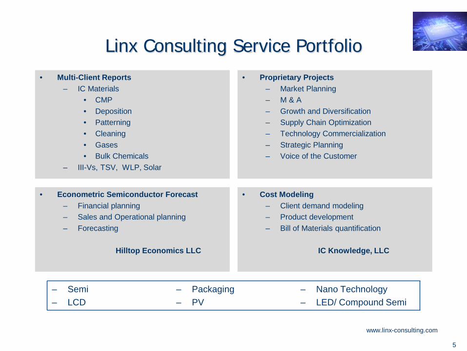
Linx Consulting Service Portfolio• Multi-Client Reports
– IC Materials• CMP• Deposition• Patterning• Cleaning• Gases• Bulk Chemicals
– III-Vs, TSV, WLP, Solar
• Proprietary Projects– Market Planning– M & A– Growth and Diversification– Supply Chain Optimization– Technology Commercialization– Strategic Planning– Voice of the Customer
• Econometric Semiconductor Forecast– Financial planning– Sales and Operational planning– Forecasting
Hilltop Economics LLC
• Cost Modeling– Client demand modeling– Product development– Bill of Materials quantification
IC Knowledge, LLC
– Semi– LCD
– Packaging– PV
– Nano Technology– LED/ Compound Semi

www.linx-consulting.com
6
Customer Base in Semiconductors
Finance &Technology
Raws & Chemicals Equipment Services End-users &
Consortia
North America
China
SEA & India
Europe
Japan
Korea
Taiwan

www.linx-consulting.com
7
Where Have We Beenand Where are We Going?

www.linx-consulting.com
8
3,000
2,500
2,000
1,500
1,000
500
75,000
70,000
65,000
60,000
55,000
50,000
45,000
40,000
35,00094 96 98 00 02 04 06 08 10 12 14
Semi MSIWorld Real GDP (Rt Scale)
Million Square Inches Billion 2010 US$
93-15Q495% correlation
MSI Multiple: 2.1X
Silicon Follows GDP Closely
1.0X
2.4X
Source: Hilltop Economics
Macro
www.linx-consulting.com
9
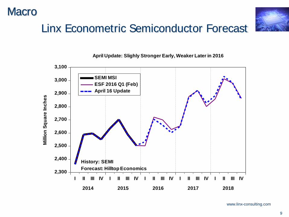
Linx Econometric Semiconductor Forecast
2,300
2,400
2,500
2,600
2,700
2,800
2,900
3,000
3,100
I II III IV I II III IV I II III IV I II III IV I II III IV
2014 2015 2016 2017 2018
SEMI MSIESF 2016 Q1 (Feb)April 16 Update
History: SEMIForecast: Hilltop Economics
April Update: Slighly Stronger Early, Weaker Later in 2016
Mill
ion
Squa
re In
ches
Macro

www.linx-consulting.com
10
Sputter Target Market $M Vs. MSI
7,000
7,500
8,000
8,500
9,000
9,500
10,000
10,500
11,000
$500
$520
$540
$560
$580
$600
$620
$640
$660
2010 2011 2012 2013 2014 2015 2016
Macro

www.linx-consulting.com
11
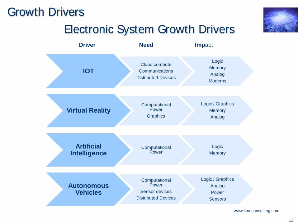
Electronic System Growth DriversGrowth Drivers
Internet of ThingsMuch hyped driver of billions of networked devices generating information for governmental, commercial, consumer, medical, and other information systems
Virtual RealityCreation of virtual displays of real and simulated environments for military, consumer, commercial and other applications, usually through a novel head display
Artificial IntelligenceComputer based intelligent learning systems
Autonomous VehiclesSensor systems supporting vehicle based computer systems offering various degrees of driver assistance including fully autonomous driverless vehicles.
www.linx-consulting.com
12
IOTCloud compute
Communications Distributed Devices
Logic MemoryAnalog
Modems
Virtual RealityComputational
PowerGraphics
Logic / GraphicsMemoryAnalog
Artificial Intelligence
Computational Power
LogicMemory
Autonomous Vehicles
ComputationalPower
Sensor devicesDistributed Devices
Logic / GraphicsAnalogPower
Sensors
Electronic System Growth DriversGrowth Drivers
Driver Need Impact
www.linx-consulting.com
13
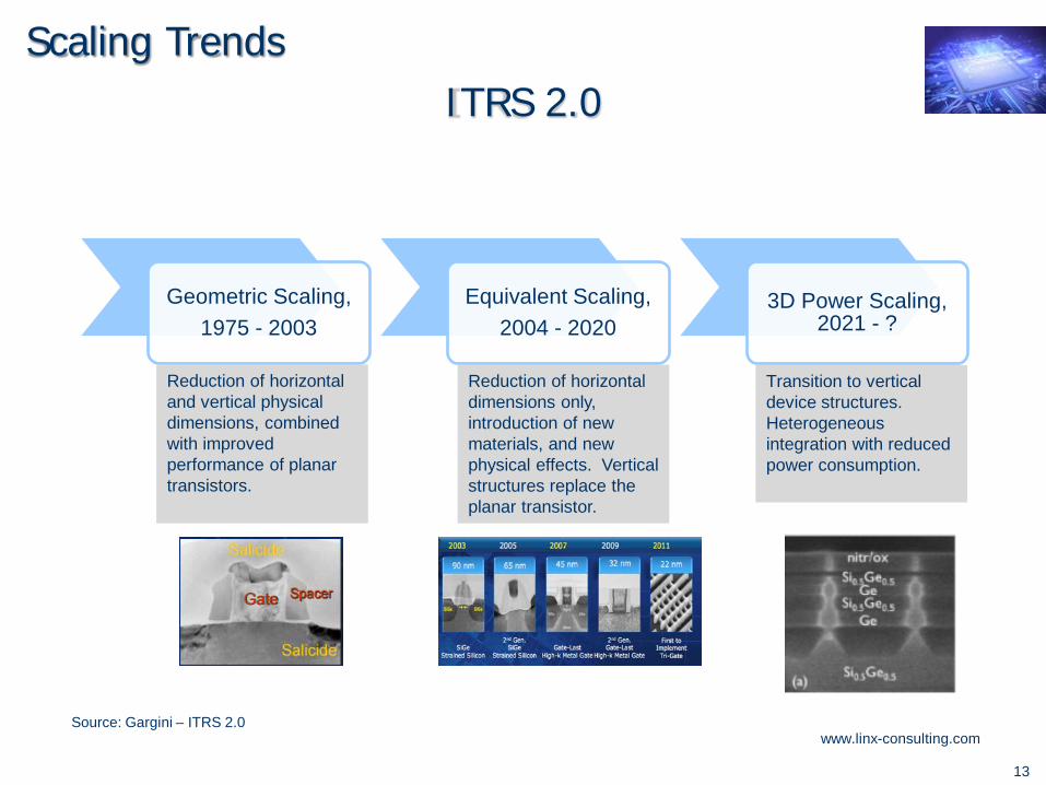
ITRS 2.0
Geometric Scaling,1975 - 2003
Equivalent Scaling,2004 - 2020
3D Power Scaling, 2021 - ?
Reduction of horizontal and vertical physical dimensions, combined with improved performance of planar transistors.
Reduction of horizontal dimensions only, introduction of new materials, and new physical effects. Vertical structures replace the planar transistor.
Transition to vertical device structures. Heterogeneous integration with reduced power consumption.
Source: Gargini – ITRS 2.0
Scaling Trends

www.linx-consulting.com
14
Materials That Enable Moore’s Law
(PM: Patterning Materials)
(IL: InterfaceLayer)sSOI/GeOI
Ge IL III-V ILGaN InSb
InGaAs Ge
STORu
Other PM's EUV
Other PM's EUV
Co Si(C)P
Co Si(C)P
FDSOISiC
FDSOISiC
Air SiCO
Air SiCO
LaO LaOLT SiO LT SiO
SiCN SiCN SiCNTiAlC MG
ZrO Hf(Si)O
AlO
TiAlC MGZrO
Hf(Si)OAlO
TiAlC MGZrO
Hf(Si)OAlO
pSiOC pSiOC pSiOCSOI SOI SOI
SiGe(B)TaO SOG
TaO SOG
SiGe(B)TaO SOG
SiGe(B)TaO SOG
SiOCTa/TaN
Cu SiOF
SiOCTa/TaN
Cu SiOF
SiOCTa/TaN
Cu SiOF
SiOCTa/TaN
Cu SiOF
TiSi PtSi
TiSi PtSi
TiSi PtSi
TiSi PtSi
TiSi PtSi
TiW TiW TiW/TiN TiN TiN TiNWSi, MoSi WSi, W WSi, W W W W
AlBPSG
AlBPSG
AlBPSG
AlBPSG
AlBPSG
AlBPSG
AlBPSG
AlSiO, SiN SiO, SiN SiO, SiN SiO, SiN SiO, SiN SiO, SiN SiO, SiN SiO, SiN
Si Si Si Si Si Si Si Si
1960 1970 1980 1990 2000 2010 2015 2020(*)
(*): Projection
Patterning RelatedBEOLFEOLStarting Materials
Source: ASM
Scaling Trends

www.linx-consulting.com
15
Linx Materials Index
$0.60
$0.65
$0.70
$0.75
$0.80
$0.85
$0.90
$0.95
$1.00
$1.05
$1.10
2010 2011 2012 2013 2014 2015 2016 2017 2018 2019 2020
$/sqin Volume slowdownASP decline
Process complexityModest growth Process simplification
Modest growth
Scaling Trends
www.linx-consulting.com
16
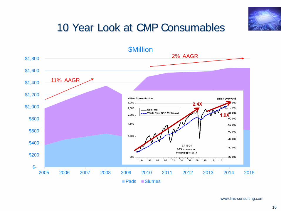
10 Year Look at CMP Consumables
$-
$200
$400
$600
$800
$1,000
$1,200
$1,400
$1,600
$1,800
2005 2006 2007 2008 2009 2010 2011 2012 2013 2014 2015
$Million
Pads Slurries
11% AAGR
2% AAGR
www.linx-consulting.com
17
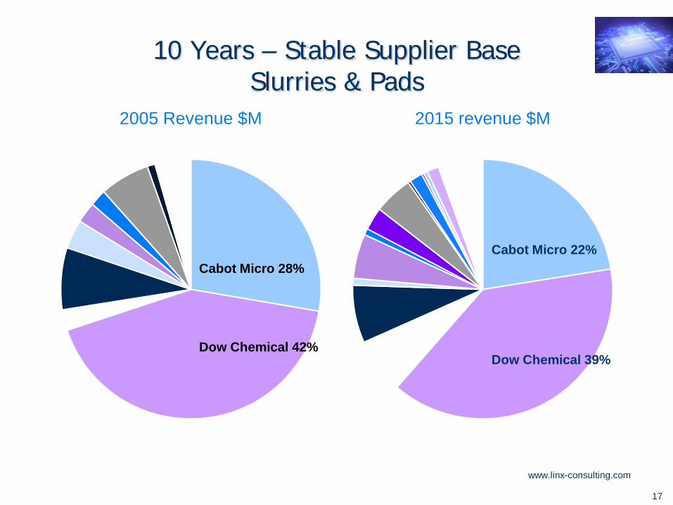
10 Years – Stable Supplier BaseSlurries & Pads
2005 Revenue $M
Cabot Micro 28%
Dow Chemical 42%
2015 revenue $M
Cabot Micro 22%
Dow Chemical 39%

www.linx-consulting.com
18
Industry Evolution
www.linx-consulting.com
19
Defectivity Paradigm Shift at 20nm
1. Pursuit of Moore’s Law is driving ever increasing design innovation, process sensitivity & complexity
2. Paradigm shift in thoughts about what we did not care about earlier in >20nm era & whatwe care to control now!
• Complex Chemistry: Compatibility Issues
• New Defect Sources, increase Defect Sensitivity
3. Metrology techniques of all types are challenged to provide sufficient sensitivity for early detection & prevention
• Supplier Infrastructure Development needed for better defect detection & characterization
• Metrology and Quality Control
4. Proactive engagement and collaboration across the supply chain are essential to HVMreadiness
Source: A. Sengupta, Intel. Semicon West 2015
The Challenge
www.linx-consulting.com
20
Defectivity
• Real-time metrology is practically impossible.• In-line metrology is challenged to measure critical particle sizes below 20nm
– High cost of systems– Off-line analysis to augment particle characterization
• Optical (particle detection) systems such as SP3 and SP5 are identifying new defects– On-wafer metrology has become the only approach able to show defects.– In many cases it is possible to identify the source from on-wafer analysis.– The expectation for particle shedding, and contamination continues to reduce.
• Killer defects, or critical particles are now in the order of 10 or 20 nm.– On-wafer analysis is struggling to define particles sizes or discriminate defects as
residues or discrete solids. – Defect sources vary from chemicals, water, seals, filters, piping etc.
• Equipment suppliers are driving to deliver ultraclean products which are certified with the latest analytical techniques, and targeted at delivering best possible performance.
The Challenge
www.linx-consulting.com
21
Wafer Fab Expectations1. Suppliers should use best practices for control of materials, manufacturing equipment,
and components– Close sub supplier collaboration and integrated quality systems; Vertical integration where
possible– Material and component control is critical
• Material and process control critical• SPC and excursion control is key• Sub-supplier involvement in quality is necessary
2. Advanced statistical process control– Feed forward and feedback SPC– Sophisticated analytical tools– Metrology and analysis gaps, demand collaboration between suppliers and users.
3. Holistic approach to defect control and Design for cost and environmental impact– Collaborative problem-solving helps identify problems quicker, and implement better
solutions – Products and systems need to be optimized for advanced node chemistries and processes
Aqueous and environmentally friendly formulations are preferred– Standardization required to reduce cost
The Challenge
www.linx-consulting.com
22
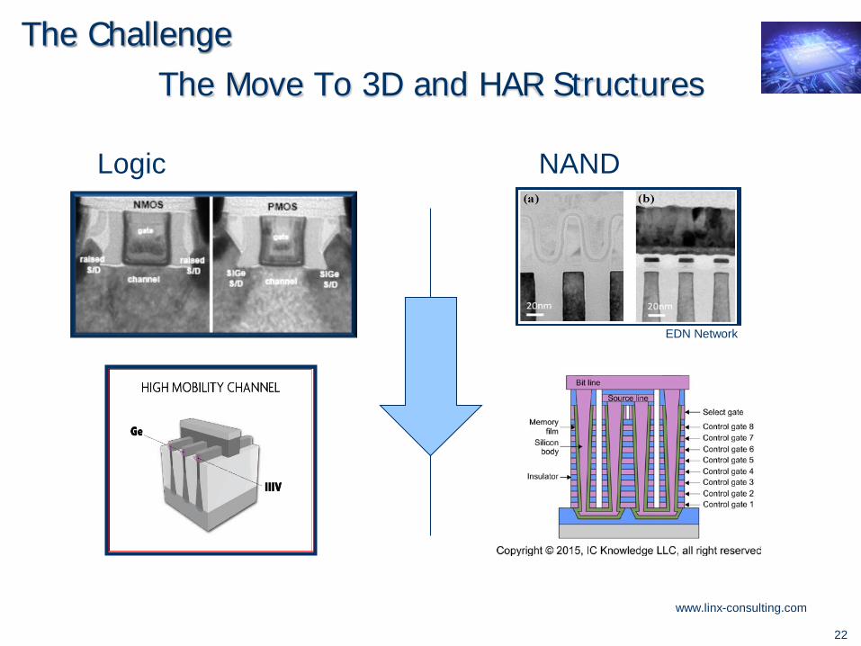
The Move To 3D and HAR Structures
Logic NAND
EDN Network
The Challenge
www.linx-consulting.com
23
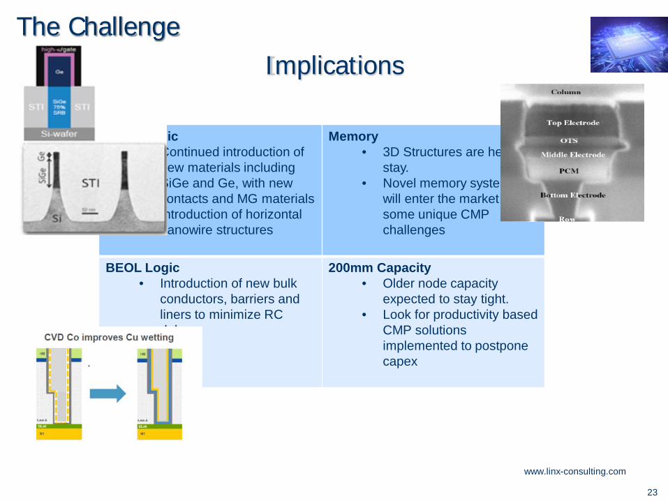
Implications
FEOL Logic• Continued introduction of
new materials including SiGe and Ge, with new contacts and MG materials
• Introduction of horizontal nanowire structures
Memory• 3D Structures are here to
stay.• Novel memory systems
will enter the market with some unique CMP challenges
BEOL Logic• Introduction of new bulk
conductors, barriers and liners to minimize RC delay.
200mm Capacity• Older node capacity
expected to stay tight. • Look for productivity based
CMP solutions implemented to postpone capex
The Challenge
www.linx-consulting.com
24
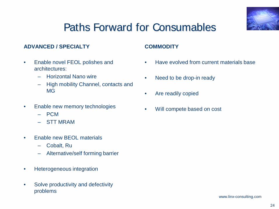
Paths Forward for Consumables
ADVANCED / SPECIALTY
• Enable novel FEOL polishes and architectures:
– Horizontal Nano wire– High mobility Channel, contacts and
MG
• Enable new memory technologies– PCM– STT MRAM
• Enable new BEOL materials– Cobalt, Ru– Alternative/self forming barrier
• Heterogeneous integration
• Solve productivity and defectivity problems
COMMODITY
• Have evolved from current materials base
• Need to be drop-in ready
• Are readily copied
• Will compete based on cost
www.linx-consulting.com
25
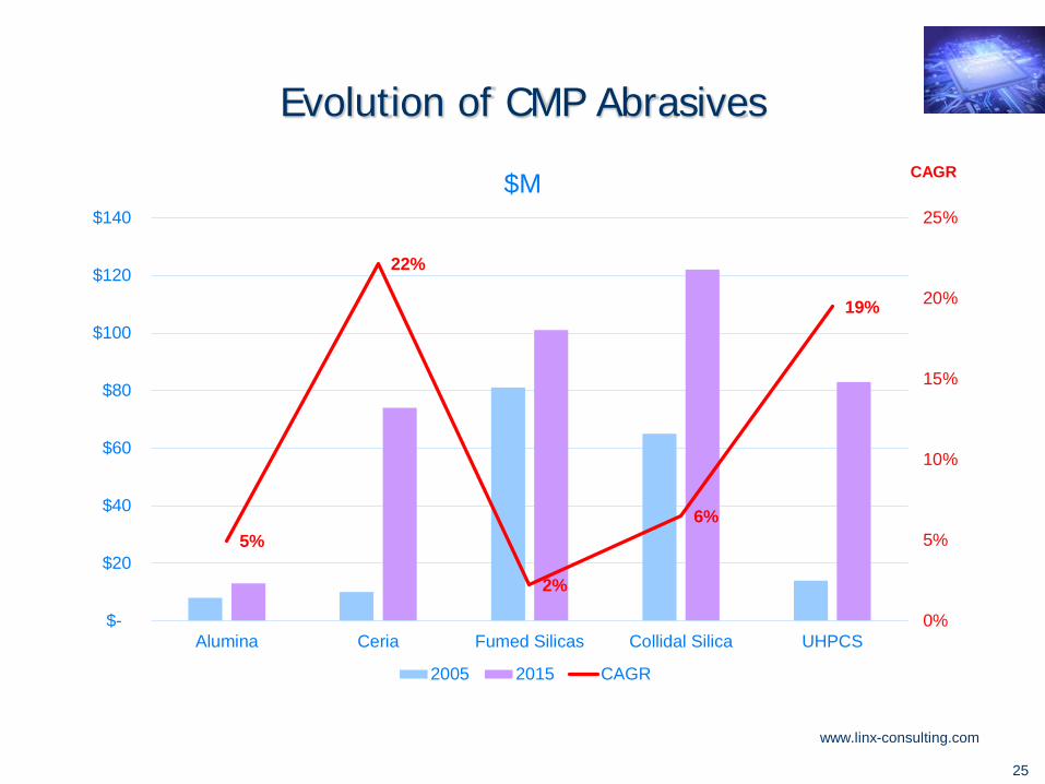
Evolution of CMP Abrasives
5%
22%
2%
6%
19%
0%
5%
10%
15%
20%
25%
$-
$20
$40
$60
$80
$100
$120
$140
Alumina Ceria Fumed Silicas Collidal Silica UHPCS
$M
2005 2015 CAGR
CAGR
www.linx-consulting.com
26
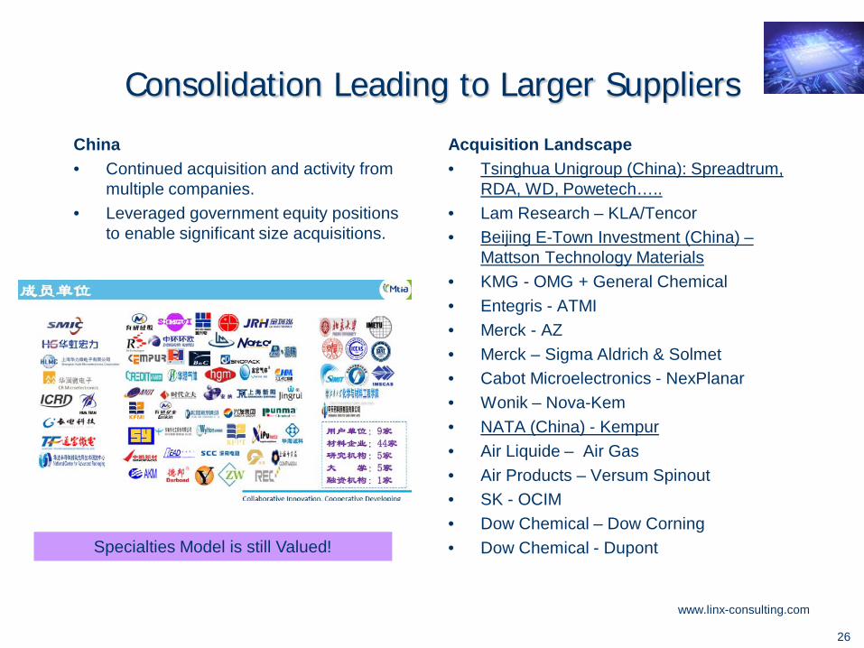
Consolidation Leading to Larger Suppliers
China• Continued acquisition and activity from
multiple companies.• Leveraged government equity positions
to enable significant size acquisitions.
Acquisition Landscape• Tsinghua Unigroup (China): Spreadtrum,
RDA, WD, Powetech…..• Lam Research – KLA/Tencor• Beijing E-Town Investment (China) –
Mattson Technology Materials• KMG - OMG + General Chemical• Entegris - ATMI• Merck - AZ• Merck – Sigma Aldrich & Solmet• Cabot Microelectronics - NexPlanar• Wonik – Nova-Kem • NATA (China) - Kempur • Air Liquide – Air Gas• Air Products – Versum Spinout• SK - OCIM • Dow Chemical – Dow Corning• Dow Chemical - Dupont Specialties Model is still Valued!
www.linx-consulting.com
27
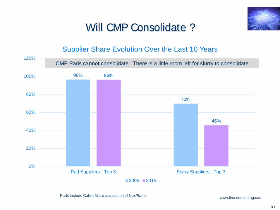
Will CMP Consolidate ?
96%
70%
96%
46%
0%
20%
40%
60%
80%
100%
120%
Pad Suppliers - Top 3 Slurry Suppliers - Top 3
Supplier Share Evolution Over the Last 10 Years
2005 2015
Pads include Cabot Micro acquisition of NexPlanar
CMP Pads cannot consolidate. There is a little room left for slurry to consolidate

www.linx-consulting.com
28
Conclusions
• Drivers for industry growth are changing, but there will continued demand for current device types
• Roadmap trends will drive to 3D device architectures in the medium to long term. System specific hybrid packages, device types, and device architectures will extend the roadmap.
• New device architectures will shift requirements of critical materials for different devices.– Lithography extension is a primary cost driver.– 3D devices will challenge aspect ratios, placing focus on etch and deposition
capabilities.
• The shift from planar scaling to 3D will extend into the packaging realm as some functionality and interconnect is moved into the wafer level package.
• Quality and defectivity requirements continue to be incredibly challenging, and require supply chain engagement.