evb hw user guide
TRANSCRIPT
Telit Evaluation Board (EVB) HW User Guide
Doc#: 1VV0301249 Rev.1.0 – 2018-01-23
EVB HW User Guide Doc#: 1VV0301249
Rev. 1.0 Page 2 of 60 2018-01-23
SPECIFICATIONS ARE SUBJECT TO CHANGE WITHOUT NOTICE
NOTICE While reasonable efforts have been made to assure the accuracy of this document, Telit assumes no liability resulting from any inaccuracies or omissions in this document, or from use of the information obtained herein. The information in this document has been carefully checked and is believed to be reliable. However, no responsibility is assumed for inaccuracies or omissions. Telit reserves the right to make changes to any products described herein and reserves the right to revise this document and to make changes from time to time in content hereof with no obligation to notify any person of revisions or changes. Telit does not assume any liability arising out of the application or use of any product, software, or circuit described herein; neither does it convey license under its patent rights or the rights of others. It is possible that this publication may contain references to, or information about Telit products (machines and programs), programming, or services that are not announced in your country. Such references or information must not be construed to mean that Telit intends to announce such Telit products, programming, or services in your country.
COPYRIGHTS This instruction manual and the Telit products described in this instruction manual may be, include or describe copyrighted Telit material, such as computer programs stored in semiconductor memories or other media. Laws in the Italy and other countries preserve for Telit and its licensors certain exclusive rights for copyrighted material, including the exclusive right to copy, reproduce in any form, distribute and make derivative works of the copyrighted material. Accordingly, any copyrighted material of Telit and its licensors contained herein or in the Telit products described in this instruction manual may not be copied, reproduced, distributed, merged or modified in any manner without the express written permission of Telit. Furthermore, the purchase of Telit products shall not be deemed to grant either directly or by implication, estoppel, or otherwise, any license under the copyrights, patents or patent applications of Telit, as arises by operation of law in the sale of a product.
COMPUTER SOFTWARE COPYRIGHTS The Telit and 3rd Party supplied Software (SW) products described in this instruction manual may include copyrighted Telit and other 3rd Party supplied computer programs stored in semiconductor memories or other media. Laws in the Italy and other countries preserve for Telit and other 3rd Party supplied SW certain exclusive rights for copyrighted computer programs, including the exclusive right to copy or reproduce in any form the copyrighted computer program. Accordingly, any copyrighted Telit or other 3rd Party supplied SW computer programs contained in the Telit products described in this instruction manual may not be copied (reverse engineered) or reproduced in any manner without the express written permission of Telit or the 3rd Party SW supplier. Furthermore, the purchase of Telit products shall not be deemed to grant either directly or by implication, estoppel, or otherwise, any license under the copyrights, patents or patent applications of Telit or other 3rd Party supplied SW, except for the normal non-exclusive, royalty free license to use that arises by operation of law in the sale of a product.

EVB HW User Guide Doc#: 1VV0301249
Rev. 1.0 Page 3 of 60 2018-01-23
USAGE AND DISCLOSURE RESTRICTIONS
I. License Agreements The software described in this document is the property of Telit and its licensors. It is furnished by express license agreement only and may be used only in accordance with the terms of such an agreement.
II. Copyrighted Materials Software and documentation are copyrighted materials. Making unauthorized copies is prohibited by law. No part of the software or documentation may be reproduced, transmitted, transcribed, stored in a retrieval system, or translated into any language or computer language, in any form or by any means, without prior written permission of Telit
III. High Risk Materials Components, units, or third-party products used in the product described herein are NOT fault-tolerant and are NOT designed, manufactured, or intended for use as on-line control equipment in the following hazardous environments requiring fail-safe controls: the operation of Nuclear Facilities, Aircraft Navigation or Aircraft Communication Systems, Air Traffic Control, Life Support, or Weapons Systems (High Risk Activities"). Telit and its supplier(s) specifically disclaim any expressed or implied warranty of fitness for such High Risk Activities.
IV. Trademarks
TELIT and the Stylized T Logo are registered in Trademark Office. All other product or service names are the property of their respective owners.
V. Third Party Rights
The software may include Third Party Right software. In this case you agree to comply with all terms and conditions imposed on you in respect of such separate software. In addition to Third Party Terms, the disclaimer of warranty and limitation of liability provisions in this License shall apply to the Third Party Right software.
TELIT HEREBY DISCLAIMS ANY AND ALL WARRANTIES EXPRESS OR IMPLIED FROM ANY THIRD PARTIES REGARDING ANY SEPARATE FILES, ANY THIRD PARTY MATERIALS INCLUDED IN THE SOFTWARE, ANY THIRD PARTY MATERIALS FROM WHICH THE SOFTWARE IS DERIVED (COLLECTIVELY “OTHER CODE”), AND THE USE OF ANY OR ALL THE OTHER CODE IN CONNECTION WITH THE SOFTWARE, INCLUDING (WITHOUT LIMITATION) ANY WARRANTIES OF SATISFACTORY QUALITY OR FITNESS FOR A PARTICULAR PURPOSE.
NO THIRD PARTY LICENSORS OF OTHER CODE SHALL HAVE ANY LIABILITY FOR ANY DIRECT, INDIRECT, INCIDENTAL, SPECIAL, EXEMPLARY, OR CONSEQUENTIAL DAMAGES (INCLUDING WITHOUT LIMITATION LOST PROFITS), HOWEVER CAUSED AND WHETHER MADE UNDER CONTRACT, TORT OR OTHER LEGAL THEORY, ARISING IN ANY WAY OUT OF THE USE OR DISTRIBUTION OF THE OTHER CODE OR THE EXERCISE OF ANY RIGHTS GRANTED UNDER EITHER OR BOTH THIS LICENSE AND THE LEGAL TERMS APPLICABLE TO ANY SEPARATE FILES, EVEN IF ADVISED OF THE POSSIBILITY OF SUCH DAMAGES.

EVB HW User Guide Doc#: 1VV0301249
Rev. 1.0 Page 4 of 60 2018-01-23
APPLICABILITY TABLE
This documentation applies to the following products:
Table 1: Applicability Table
Module Name Description
LE920A4
xE922-3GR
LE910Cx
LE910Cx - mPCIe
LE940A6
LE940A9
LE940B6
NE866B1
NL865B1
ME866E1
EVB HW User Guide Doc#: 1VV0301249
Rev. 1.0 Page 5 of 60 2018-01-23
CONTENTS
1. INTRODUCTION .............................................................................................7
Scope ............................................................................................................. 7
Audience......................................................................................................... 7
Contact Information, Support .......................................................................... 7
Text Conventions ............................................................................................ 8
Related Documents ........................................................................................ 8
2. PRODUCT DESCRIPTION ..............................................................................9
Overview......................................................................................................... 9
Block Diagram ...............................................................................................11
Default Jumper Placement .............................................................................13
3. POWER SUPPLY .......................................................................................... 16
Supply Source Selection ................................................................................16
Module Supply Current Monitoring .................................................................19
Auxiliary Supply .............................................................................................20
Battery Charging ............................................................................................21
4. CONTROL SWITCHES AND INDICATOR LEDS .......................................... 22
Telit Module ...................................................................................................22
Control Buttons ..............................................................................................22 4.2.1. ON/OFF .........................................................................................................23 4.2.2. Reset .............................................................................................................23 4.2.3. Shutdown (SHDN) .........................................................................................23 4.2.4. ECALL ...........................................................................................................23 4.2.5. EMERGENCY BOOT.....................................................................................23 4.2.6. Remote Controlling of the Buttons .................................................................24
Battery Charger .............................................................................................24
A-Star ............................................................................................................25
GPS LNA Control ...........................................................................................25
5. INTERFACES ................................................................................................ 26
SIM Interface .................................................................................................26 5.1.1. SIM1+eSIM Configuration (PL202) ................................................................26 5.1.1.1. EVB SIM1 Configuration (PL201) ..................................................................27 5.1.2. SIM2 ..............................................................................................................28
USB Interface ................................................................................................28
UART Interface ..............................................................................................29
Micro SD Card Interface ................................................................................29

EVB HW User Guide Doc#: 1VV0301249
Rev. 1.0 Page 6 of 60 2018-01-23
JTAG Interface...............................................................................................29
6. ANALOG AUDIO ........................................................................................... 30
Audio Connector Selection ............................................................................30 6.1.1. 3.5-mm Audio Jack Configurations ................................................................31 6.1.1.1. Configuring 3.5-mm Audio Jack to a Stereo + MIC ........................................31 6.1.1.2. Configuring MIC BIAS ....................................................................................32 6.1.1.3. 3.5-mm Jack Detection (HS DET) Feature .....................................................33 6.1.2. RJ11 Phone Type Socket Configuration ........................................................34 6.1.2.1. Configuring MIC BIAS ....................................................................................36
MEMS Microphone ........................................................................................37
Class D Amplifier ...........................................................................................39
7. THERMAL MONITORING & COOLING ........................................................ 41
Thermal Monitoring ........................................................................................41
Cooling ..........................................................................................................41
8. CONNECTORS ............................................................................................. 42
IO Connectors ...............................................................................................42
120-pin Male B2B Connectors .......................................................................44
Extension Connector .....................................................................................48
9. EVB COMPONENT DIAGRAM ..................................................................... 50
10. SCHEMATICS ............................................................................................... 52
11. SAFETY RECOMMENDATIONS................................................................... 57
12. ACRONYMS .................................................................................................. 58
13. DOCUMENT HISTORY ................................................................................. 59

EVB HW User Guide Introduction Doc#: 1VV0301249 Scope
Rev. 1.0 Page 7 of 60 2018-01-23
1. Introduction
Scope
This document introduces and describes Telit’s generic Evaluation Board.
Audience
This document is intended for Telit customers, especially SW and system integrators, about to implement their applications using Telit products.
Contact Information, Support
For general contact, technical support services, technical questions and report documentation errors, contact Telit Technical Support at:
• [email protected] • [email protected] • [email protected] • [email protected]
Alternatively, use:
http://www.telit.com/support
For detailed information about where you can buy the Telit modules or for recommendations on accessories and components visit:
http://www.telit.com
To register for product news and announcements or for product questions contact Telit’s Technical Support Center (TTSC).
Our aim is to make this guide as helpful as possible. Keep us informed of your comments and suggestions for improvements.
Telit appreciates feedback from the users of our information.

EVB HW User Guide Introduction Doc#: 1VV0301249 Text Conventions
Rev. 1.0 Page 8 of 60 2018-01-23
Text Conventions
The following conventions are used to emphasize specific types of information:
DANGER: Danger – This information MUST be followed or catastrophic equipment failure or bodily injury may occur.
WARNING: Caution or Warning – Alerts the user to important points about integrating the module, if these points are not followed, the module and end user equipment may fail or malfunction.
NOTE: Tip or Information – Provides advice and suggestions that may be useful when integrating the module.
All dates are in ISO 8601 format, i.e. YYYY-MM-DD.
Related Documents
Table 2: Related Documents
Document Title Document Number
Ref 1: Telit EVB Arduino User Guide 80000NT11509A

EVB HW User Guide Product Description Doc#: 1VV0301249 Overview
Rev. 1.0 Page 9 of 60 2018-01-23
2. Product Description
Overview
The Telit Evaluation Board is a generic developer’s platform, which is designed to provide the complete development environment to the user and intended to be used with a new set of Telit IoT modules as listed in the Applicability Table.
The EVB is designed to carry an Interface Board (IFBD) via three 120-pin B2B connectors, thus making the EVB seamless to an actual size or pinout so that it can support multiple form factors and products.
The Telit module is mounted directly on the IFBD.
Power supply and control interface to the IFBD module are provided from the EVB via the B2B connectors. Several power supply configurations, including battery charging, are available. In addition, all interfaces needed for the developers, such as SIM card holders, JTAG, UART, USB, audio, micro SD, etc., are available on the EVB main board.
To offer remote control and/or test automation of the EVB environment, the EVB can be equipped with an Arduino-compatible, A-star 32U4 microcontroller board, based on Atmel’s Atmega32U4 with USB interface. This Arduino-compatible card is mounted on the EVB using two 10-pin headers.
The EVB functionality and supported features can be extended using the 120-pin SAMTEC extension connector (EXT) which allows adding an additional Extension Card to the system, such as SGMII Ethernet MAC/PHY, WiFi, audio codec, display, camera, Dead Reckoning (DR), etc.
Refer to your Telit representative for more information about the available extension cards that suit the Telit product designed into your application.

EVB HW User Guide Product Description Doc#: 1VV0301249 Overview
Rev. 1.0 Page 10 of 60 2018-01-23
Figure 1 shows a typical EVB platform consisting of an EVB main board and an IFBD (IFBD of the Telit LE920 module as an example).
Figure 1: EVB with IFBD on Top

EVB HW User Guide Product Description Doc#: 1VV0301249 Block Diagram
Rev. 1.0 Page 11 of 60 2018-01-23
Block Diagram
Figure 2 is a high-level system overview of the generic EVB development platform.
Figure 2: EVB System Overview
The Extension Card section shown in Figure 2 is only an example of some of the possible EXT Card options that can be developed for the EVB.
Contact your Telit representative for the list of available extension cards that can be used for your specific product/application.
USIF 2
ON/OFF
0
LED 3
uSDMIC2MIC1
EP1EP2
RJ11
JTAG
USB 2.0 / USB 3.0
I2S SPI DSI CSI1 CSI 2
Charger
I2C
VBATT_AUX
VBATT
GPIO
Arduino A-Star 32U4 Micro
ON/OFF
RESET0
0
PWR_EN
Remote/Debug Functions
FTDIUART2USB
From any of EVBUSB connections
VBATT
Meas
Meas
PWR_EN(Remote)Meas
VBATT
VBATT_PA
3.8V 5AVR
On-Board Power
SIM 1SIM SW (2:1)NX3DV2567 SIM 1
eSIM
ANT 2 ANT 3ANT 1
B2B
B2B
B2B
Key
EVBGeneric Main Card
EVB Connectivity
Interface Card
Extension Cards
SuperCap
From Temp_Sensor
Temp_Sensor
Current Measure
FAN
SIM 2
HP
RESETKey
VR Bypass (3.8V-4.2V)
VBATT AUX
PCM PWR
SPKR AMP
MAC
120 Pin Edge Connector
6V-12V
MMI Card WiFi Ext
CodecSPI
Flash BT ETHPHY

EVB HW User Guide Product Description Doc#: 1VV0301249 Block Diagram
Rev. 1.0 Page 12 of 60 2018-01-23
Figure 3 shows a more detailed block diagram of the EVB main board.
Figure 3: EVB Main Board Block Diagram
NOTE: Items that appear in red color in the diagram are mounted on the bottom side.

EVB HW User Guide Product Description Doc#: 1VV0301249 Default Jumper Placement
Rev. 1.0 Page 13 of 60 2018-01-23
Default Jumper Placement
Normally, EVB kits should be pre-configured according to the following default jumper placement, which corresponds to the regular mode for SW development and functional use.
Main assumptions/conditions: • Power source by SMPS down convertor (set-point 3.9V) fed from PL101/SO101 • SIM device placed in SIM1 cardholder SO202 • Audio downlink:
o 3.5mm audio jack uses EAR1 for L-CH and EAR2 to R-CH. o RJ11 is not connected. o Speaker connected directly (D Class AMP bypassed)
• Audio uplink: o 3.5mm audio jack uses MIC1 (Single-ended mode). o On-board MEMS microphone uses MIC2.
• Current measure resistors shorted (bypassed)
Figure 4: Default Jumper Setting

EVB HW User Guide Product Description Doc#: 1VV0301249 Default Jumper Placement
Rev. 1.0 Page 14 of 60 2018-01-23
Table 3 summarizes the default jumper settings. Use the following jumper types: • For 2.56 mm jumpers, use PN 1FFPJ00100. • For 1.27 mm jumpers, use PN 1FF0600633HRW.
NOTE: The default jumper settings shown here reflect the latest HW revision of the EVB. For previous versions, refer to previous versions of this document.
Table 3: Default Jumper Settings
Jumper Jumper Type Set Position Description
PL103 2.54 mm 2-3 SO101/PL101 sources SMPS
PL106 2.54 mm 1-2 No direct feed by PL102 (bypass)
PL105 2.54 mm 2-3 SMPS path selected
PL114, PL108
2.54 mm 1-2 Spare
PL111 2.54 mm 1-2/3-4 No current measurement
PL112 2.54 mm 1-2/3-4 No current measurement
PL109/ PL110
2.54 mm 2/2 VBAT_AUX = Main VBAT
PL204 2.54 mm 2-3 USB switch connected to SO203
PL206 2.54 mm 1-2 SPI (SO208) VREG_MSME
PL302 2.54 mm Open No SIM Detect control by A-star
PL202 2.54 mm 2-3 Use external SIM device
PL201 2.54 mm 1-2 Use SIM1 cardholder
PL411 2.54 mm Open Enable external 3V Bias
PL402 1.27 mm 1-3
4-6
MIC1 uses single-ended mode
RJ11 Mic Bias = External 3V EVB Bias

EVB HW User Guide Product Description Doc#: 1VV0301249 Default Jumper Placement
Rev. 1.0 Page 15 of 60 2018-01-23
Jumper Jumper Type Set Position Description
PL403 1.27 mm 1-3
4-6
Microphone of the 3.5mm audio jack connected to MIC1
3.5mm audio jack Mic Bias = External 3V EVB Bias
PL404 1.27 mm 1-3/2-4 EAR1 to 3.5mm audio jack Right channel (SO401)
PL405 1.27 mm 1-3/2-4 EAR2 to 3.5mm audio jack Left channel (SO401)
PL406 Open Microphone of RJ11 is not connected
PL407 1.27 mm 3-5
4-6
MEMS mic connected to MIC2
MEMS Mic Bias = External 3V EVB Bias
PL408 1.27 mm Pin 5 (single)
Pin 6 (single)
2 spare jumpers
PL409 1.27 mm 3-5
2-4
GPS bias controlled via GPIO
Class D amp shutdown
PL414 1.27 mm 3-5
4-6
Speaker Right connected directly (Class D bypassed)
Speaker Left connected directly (Class D bypassed)

EVB HW User Guide Power Supply Doc#: 1VV0301249 Supply Source Selection
Rev. 1.0 Page 16 of 60 2018-01-23
3. Power Supply
Supply Source Selection
The EVB can be configured for different power supply sources depending on the required use case. The following block diagram shows the different power path options.
Figure 5: EVB Power Supply
The EVB main power connector is PL101/SO101 with an input range of 6-15V.
Normally (i.e. in a typical SW developers setup), the EVB is supplied from the main power connector, and a DCDC buck supply with a set point of 3.9V is used to provide the system VBAT. So the usual jumper configuration is as follows: PL103/2-3; PL106/1-2; PL105/2-3.
PL102 allows an external configurable power supply to feed directly the Telit module VBAT input supply while all the auxiliary peripherals are sourced by the main power connector. For more details, refer to Section 3.3, Auxiliary Supply.
This mode of operation is also needed to test the complete VBAT range during module certification.
For field testing, an additional backup battery can be added (connected to PL104) in the box to overcome sudden or unexpected power drops from the vehicle’s 12V source. Since the Telit module does not incorporate an internal battery charger solution, the EVB has an external charger circuit based on BQ24261M from TI.
For field testing (battery incl.) use the following jumper configuration: PL103/1-2; PL106/open; PL105/1-2.
Although strictly not necessary to be present, the A-star control board can be applied to automate the EVB power supply sequencing for testing purposes, battery charger control, as well as for other control and/or current or temperature monitoring functions.

EVB HW User Guide Power Supply Doc#: 1VV0301249 Supply Source Selection
Rev. 1.0 Page 17 of 60 2018-01-23
If the A-star module is not mounted in the system, the following default conditions apply:
• Use case of DCDC buck power path selected (PL103/2-3):
The buck supply is enabled by default and supplies the system with 3.9V.
• Use case of charger path selected (PL103/1-2):
The TI BQ24261M device offers two features:
o Power-path control o Battery charging
The power-path feature allows the BQ24261M to power the system from a high-efficiency DC-DC converter while simultaneously and independently charging the battery. The power path also permits the battery to supplement the system current requirements when the adapter cannot.
The power path can supply the system even if no battery is connected, but it is limited to 400 mA so most probably the system will not be able to reach full functionality using this mode.
The battery charging feature itself is enabled by default but is limited to 400 mA. For high current battery charging, the charger must be software-controlled and enabled over the I2C communication bus, thus the A-star module must be present and is responsible for enabling and controlling battery charging.
BQ24261 I2C SLAVE 7 bit address: 0x6B
If no input source of at least 6V is present on PL101/SO101, the charger path can also be supplied from the 5V VBUS USB connector via diodes when connected (either from the module USB connector via D106 or from the FTDI USB-UART connector via D107).
To avoid current to be drawn from the USB host(s) inadvertently, apply an external power source of at least 6V on PL101/SO101, so the Schottky diodes will be reverse polarised.
NOTE: The current sourced from typical USB hosts is usually limited to 500 mA, so check your USB (charger) source specification or make sure that the SW I2C configured battery charging current is lower.

EVB HW User Guide Power Supply Doc#: 1VV0301249 Supply Source Selection
Rev. 1.0 Page 18 of 60 2018-01-23
It is up to the user to place the jumpers according to the power system configuration he wants to apply. The following snapshots of the component diagram clarify the detailed pin locations of the jumpers related to power selection.
The suggested green-colored jumper locations can be used for typical SW developers use to supply the system from an external 6V supply without any battery presence/charging involved.
Figure 6: Jumper PL103
Figure 7: Jumpers PL105 / PL106

EVB HW User Guide Power Supply Doc#: 1VV0301249 Module Supply Current Monitoring
Rev. 1.0 Page 19 of 60 2018-01-23
Module Supply Current Monitoring
The system current of the module can be measured, using one of the following options: • The A-star module can be programmed to automate/measure/log the current
consumed by the VBATT and VBATT_PA supply lines from a host PC application. Two MAX9611AUB devices and 1%-precision resistors are used as listed in Table 4.
Table 4: I/V Convertor Settings
VBATT VBATT_PA
Sense Resistor I/V conversion
250 mOhm 50 mOhm
MAX9611 I2C Slave address (W/R)
0xE0/0xE1 0xE6/0xE7
To enable (insert) the sense resistors in the VBAT supply paths, leave the following jumper positions open:
PL111 position 3-4 (VBAT) and PL112 position 3-4 (VBAT_PA).
• An external ampere meter for manual measurements:
PL111 position1-2 and PL112 position1-2 can be opened and used to apply current clamps to an external ampere meter for manual measurements.
• Using an external power supply or power monitor/analyzer device, bypassing the PL102 input power connector:
By placing a jumper on PL106 position 2-3, you can bypass the on-board voltage regulator, connect an external power supply or power monitor/analyzer device, and use a host PC to monitor the system current directly.
This option is useful for automated test setups with a host PC controlling the full system supply voltage range (via GPIB commands) to cover RF certification.
The following snapshots clarify the detailed pin location of the jumpers involved for a typical SW Developers Use mode: PL111 and PL112, without the need for sense resistors and/or external ampere meter presence in the supply path.
The jumper positions colored in green are suggested.

EVB HW User Guide Power Supply Doc#: 1VV0301249 Auxiliary Supply
Rev. 1.0 Page 20 of 60 2018-01-23
Figure 8: Jumpers PL111/PL112
Auxiliary Supply
To avoid interference between the VBAT current path of interest, (i.e. the current actually drawn by the Telit module), and the current drawn by peripherals in the system. The VBAT_AUX supply path can be isolated from the actual current path of the Telit module.
VBAT_AUX supplies the following subsystems: • A-Star remote control module (also supplied from the main input supply if system
supply control from A-star GPIO is needed) • I/O connectors • MicroSD card supply (3.0V) • Status LEDs • GNSS external LNA supply • Class D audio amplifier • Cool fan supply • Expansion board
For maximum flexibility, a 2x3 jumper setup (PL109/PL110) allows to select the VBAT_AUX supply from 3 possible sources:
• Main system supply VBAT (= module supply): PL110 position 2 _ P109 position 2 • DCDC buck SMPS convertor output: PL109 position 1-2 • Battery charger output CHG_BAT: PL109 position 2-3

EVB HW User Guide Power Supply Doc#: 1VV0301249 Battery Charging
Rev. 1.0 Page 21 of 60 2018-01-23
Figure 9 clarifies the detailed pin position of the two jumpers involved PL109/PL110 and shows the suggested SW Developers Use settings in green color.
Figure 9: Jumpers PL109/PL110
Battery Charging
The Telit EVB includes a built-in battery that can be optionally installed. The battery can be used during field trials, drive tests, and also for demos. In addition, it can be useful during tests where a power cut is not desired.
The battery is charged using the TI BQ24261MRGER Charger IC.
The BQ24261MRGER is controlled via the A-Star Arduino I2C and enabled by Arduino GPIO0.
• Pull GPIO0 low to enable charging. • Pull GPIO0 high to disable charging and place the charger in HZ mode.
The BQ24261MRGER slave address is 0xD6.
Charging control and monitoring is done by the A-Star FW and requires the A-Star to be present.
The charging circuit includes a status LED and 2 indications. For more information, refer to Section Battery Charger on p.24.

EVB HW User Guide Control Switches and Indicator LEDs Doc#: 1VV0301249 Telit Module
Rev. 1.0 Page 22 of 60 2018-01-23
4. Control Switches and Indicator LEDs
Telit Module
The generic EVB offers 2 indication LEDs that can be used to signal the module status and state of operation.
• SW_RDY LED (yellow) • STATUS LED (red)
The actual LED functionality is determined by the Telit module in use and by the connectivity inside the IFBD. Refer to the specific IFBD user guide.
Figure 10: Module Status LEDs
Control Buttons
The following tact switches are available to control the module: • SW301: SHDN • SW303: RESET • SW302: ON/OFF • SW305: ECALL • SW501: EMERGENCY BOOT
Figure 11 shows the location of the LEDs on the EVB main board.
Figure 11: Module Control Buttons

EVB HW User Guide Control Switches and Indicator LEDs Doc#: 1VV0301249 Control Buttons
Rev. 1.0 Page 23 of 60 2018-01-23
The actual button functionality is determined by the Telit module in use and by the connectivity inside the IFBD. Refer to the specific IFBD user guide.
Not all buttons are used or active with all types of Telit modules. The description below is one example that suits some of the modules.
4.2.1. ON/OFF
The normal power-on/off cycle of the module is controlled by the ON/OFF button. • Normally, the user presses this button to power ON the module. • Normally, the user presses this button to power OFF the module, allowing graceful
software-controlled power-off.
4.2.2. Reset
Normally, the RESET button is connected to the main Reset of the module in use.
4.2.3. Shutdown (SHDN)
On some modules, pressing the SHDN button triggers the PMIC device to execute a “forced” power supply shutdown (without allowing the software to end all ongoing activities on the modem device properly). It is comparable to a system power cut, but is not entirely the same, since the PMIC still follows the proper power-off cycle started with a modem reset assertion.1
4.2.4. ECALL
For automotive modules, the ECALL button (connected to TGPIO_20) can be used to trigger an ECALL event. On some modules, this button has dual functionality and can be used during boot to trigger/force the module into SW download mode.
The actual button functionality is determined by the Telit module in use and by the connectivity inside the IFBD.
4.2.5. EMERGENCY BOOT
The actual button functionality is determined by the Telit module in use and by the connectivity inside the IFBD.
This button is relevant for specific modules while on others, it is simply not connected or can be used for other purposes.
In those specific modules, holding down the EMERGENCY BOOT button during module power-up will force the module to enter into the chipset bootloader (during execution of chipset BootROM).
1 The Arduino A-star controller board has full control over the on_off control pin of the DCDC regulator of the EVB power circuitry. Using this way to power off the system is a “real” system power cut simulation, compared to SHDN.

EVB HW User Guide Control Switches and Indicator LEDs Doc#: 1VV0301249 Battery Charger
Rev. 1.0 Page 24 of 60 2018-01-23
4.2.6. Remote Controlling of the Buttons
Instead of by physical pressing, the ON/OFF, RESET, and SHDN buttons can also be soft-controlled from the A-star controller board, according to the following signal mapping table.
Table 5: A-Star Module Power Cycle Control
Push Button A-star Control Pin
ON/OFF D11
RESET D12
SHDN D5
Battery Charger
A single red status LED provides feedback on the BQ24261M charger device status as follows:
• During charging, the LED is turned on. • If charging is complete or disabled, the LED turns off.
Figure 12 illustrates the LED position.
Figure 12: Charger Status LED
In addition to the LED, the charger has 2 indication signals that can also be sensed by the A-star controller board, according to the following signal mapping:
Table 6: A-star Sensing of Charger Indicators
Charger Indicator A-star Sense Pin
STAT (same as the LED) D4
INT D6
This requires an A-star internal pull-up configuration on the related signals.

EVB HW User Guide Control Switches and Indicator LEDs Doc#: 1VV0301249 A-Star
Rev. 1.0 Page 25 of 60 2018-01-23
A-Star
Besides the already mentioned control and sense functions of the A-star controller board, there are a few switches impacting the A-star module itself:
• SW306: Reset button of the A-star module • SW304: 2pin-dipswitch to (optionally) define (up to) four A-star SW configuration
modes
GPS LNA Control
The generic EVB supports 2 options for providing and controlling the GPS LNA / Active antenna using PL409.
Figure 13: GPS LNA Control
The options are as follows: • Setting the PL409 jumper to 1-3 (upper left side) will constantly enable the LNA
using the EVB on-board power supply. • Setting the PL409 jumper to 3-5 (lower left side) will enable the LNA to be
controlled by a GPIO of the module.
Table 7: GPS LNA Control
PL409 A-star Control Pin
1-3 Always ON
3-5 Enabled by GPIO from the module
NOTE: Not all modules support the GPIO mode. Refer to the relevant module user guide for more information.

EVB HW User Guide Interfaces Doc#: 1VV0301249 SIM Interface
Rev. 1.0 Page 26 of 60 2018-01-23
5. Interfaces
SIM Interface
Most Telit modules offer a dual SIM interface - SIM1 and SIM2. Some of them have an embedded eSIM chip implemented in parallel on the SIM1 interface bus, adding an additional eSIM_RST signal defined on the module pinout interface.
The EVB allows for maximum flexibility by providing the following options for interfacing the SIM devices:
• SIM1 cardholder multiplexed with an EVB on-board embedded “Test eSIM” chip • SIM2 cardholder
Both SIM1 and SIM2 card holders are of the push-push type and support a full-size SIM.
To avoid SIM1 bus conflicts, each SIM placeholder has a 200k pulldown on its RST line, keeping the SIM device in that location in reset status. The modem-sourced RST signal activates the SIM device in use by overruling the pulldown connected according to the multiplex path configuration.
The section below describes the possible SIM configurations:
5.1.1. SIM1+eSIM Configuration (PL202)
PL202 defines which SIM card is physically connected to the SIM1 port: • SIM1 port is connected inside the module, i.e. an eSIM chip inside the cellular
module is used: PL202 position 1-2 • SIM1 port uses the EVB SIM1_cardholder /or/ EVB on-board eSIM chip2: PL202
position 2-3
Figure 14: PL202 for SIM1 Using the Module-internal eSIM Chip
2 The eSIM on the EVB is a “Test eSIM”, i.e. it allows the connection to test equipment (base station simulator) but not to a real life network (except using emergency mode).

EVB HW User Guide Interfaces Doc#: 1VV0301249 SIM Interface
Rev. 1.0 Page 27 of 60 2018-01-23
Figure 15: PL202 for SIM1 Port Using the EVB SIM1 Cardholder or EVB On-board Test eSIM
5.1.1.1. EVB SIM1 Configuration (PL201)
NOTE: The configuration below is valid only if PL202 is in position 2-3.
PL201 defines the actual EVB SIM connected to SIM1 port. • SIM1 port is connected to SIM1 cardholder: PL201 position 1-2 • SIM1 port is connected to the EVB on-board eSIM chip: PL201 position 2-3
Figure 16: SIM1 Port Using SIM1 Cardholder PL201
Figure 17: SIM1 Port Using the EVB External eSIM Chip PL201
For test purposes, the EVB on-board A-star controller board can control a SPDT switch (U206) to automate (emulate) SIM card removal detection use cases. This switch can change the status of the SIMIN1 detect line to “not connected”, actually simulating a SIM card removal to the software.
To enable this control, place Jumper PL302, connecting the A-star interface (pin D8) to SIMCTRL. If PL302 is not placed, SIMCTRL is set to 1, which is the default setting.

EVB HW User Guide Interfaces Doc#: 1VV0301249 USB Interface
Rev. 1.0 Page 28 of 60 2018-01-23
Table 8: SIMCTRL Truth Table
SIMCTRL SIM Card Detect Status (SIMIN1)
0 Simulated removal of SIM
1 Actual SIM card status
5.1.2. SIM2
The SIM2 port is not configurable and is directly connected to the SIM2 cardholder (SO201), which is located on the bottom side of the EVB (under the SIM1 holder).
USB Interface
The EVB provides a HS USB connection to the Telit module USB port to support the use cases below:
• Flash/update firmware • Data connection port • Diagnostics
The EVB supports USB3.0 for compatibility with future Telit modules.
The Micro USB AB connector is located on the EVB main board.
Besides routing the USB bus to this main connector, there is a second USB path available towards the extension connector SO506, which allows designing extension cards with USB connection to the USB port of the module.
The active USB path used is defined by the multiplexer switch (refer to Figure 18) which is controlled via a jumper or a GPIO.
By default, Jumper PL204 is in position 2-3, which means that the USB switch is forced to allow USB connectivity between the EVB USB connector and the Telit module as shown below.
Figure 18: USB Connectivity Jumper
If dynamic control is required, set PL204 to position 1-2. In this case, the switch will be controlled by TGPIO_02 of the Telit module.

EVB HW User Guide Interfaces Doc#: 1VV0301249 UART Interface
Rev. 1.0 Page 29 of 60 2018-01-23
Refer to the IFBD User Guide for the actual connectivity of TGPIO_02 to the module.
Table 9: USB Path Selection
TGPIO_02 Active USB Path
0 Micro-AB USB connector SO203 (default)
1 Extension connector SO506
UART Interface
The EVB includes two generic UART interfaces: • UART1 – 4-wire UART • UART2 - Auxiliary UART with 2 pins
On the EVB, both UART interfaces are routed to a dual serial-USB convertor FT2232D, accessible via mini-B USB connector SO301.
The actual mapping of the module’s UART interfaces to the EVB UART ports is defined in the IFBD. Refer to the IFBD User Guide for more information.
Micro SD Card Interface
The EVB provides a Micro-SD card socket (SO204) for cases where the Telit module supports an SD Card interface.
The EVB supports a 4-bit dual-voltage (1.8/2.95V) SD card interface.
The EVB main board allows SD 3.0 at up to 200 MHz SDR / 50 MHz DDR.
The actual speed and voltage support is determined by the module in use and the IFBD connectivity.
The EVB supports card detection as well.
On top of the digital SD interface lines, the module also provides a reference supply (VMMC) for the external pullup resistors3.
The power supply of the memory card must be sourced externally using the on-board 3.0V linear regulator (U205). The Regulator Enable pin, which is active HIGH, is connected to VMMC.
JTAG Interface
For debugging the SW code level with a JTAG pod, the standard 20-pin header connector PL203 gives access to the module chipset JTAG interface.
3 SD card pull-ups by default are present on EVB, but can be omitted if such pull-ups are available within the module (either on-board or chipset-internal).

EVB HW User Guide Analog Audio Doc#: 1VV0301249 Audio Connector Selection
Rev. 1.0 Page 30 of 60 2018-01-23
6. Analog Audio
Audio Connector Selection
The EVB board offers two generic Analog audio interface connectors: • 3.5mm stereo audio jack - SO401 • RJ11 Terminal phone type mono audio socket - PL401
The actual audio features supported by the specific module are described in the module Hardware User Guide.
The actual connectivity of the module audio interfaces to the EVB generic audio connectors is described in the relevant IFBD User Guide.
To cover all use cases and audio path multiplexing options, a jumper-based set of connectors provides a matrix of all possible audio path selections as detailed in following subsections.
Figure 19: Analog Audio Path Selection Matrix

EVB HW User Guide Analog Audio Doc#: 1VV0301249 Audio Connector Selection
Rev. 1.0 Page 31 of 60 2018-01-23
6.1.1. 3.5-mm Audio Jack Configurations
6.1.1.1. Configuring 3.5-mm Audio Jack to a Stereo + MIC
Downlink 3.5-mm audio jack: • EAR1_MT+: JACK_L • EAR1_MT-: AC coupled to GND • EAR2_MT+: JACK_R • EAR2_MT-: AC coupled to GND
Jumper configuration: • PL404: Position 1-3 & 2-4 • PL405: Position 1-3 & 2-4
Figure 20: Downlink 3.5-mm Audio Jack PL404/PL405
Uplink 3.5-mm audio jack using MIC1 path: • MIC1_MT+: JACK_MIC+ • MIC1_MT-: AC coupled to GND
Jumper configuration: • PL402: Position 1-3 • PL403: Position 1-3
Figure 21: Uplink 3.5-mm Audio Jack MIC1 PL402/PL403

EVB HW User Guide Analog Audio Doc#: 1VV0301249 Audio Connector Selection
Rev. 1.0 Page 32 of 60 2018-01-23
Uplink 3.5-mm audio jack using MIC2 path: • MIC2_MT+: JACK_MIC+ • MIC2_MT-: AC coupled to GND
Jumper configuration: • PL402: Position 3-5 • PL403: Position 3-5
Figure 22: Uplink 3.5-mm Audio Jack MIC2 PL402/PL403
6.1.1.2. Configuring MIC BIAS
The EVB provides two options for providing bias to the 3.5-mm jack microphone: MICBIAS: In this case, the bias is generated by the module’s built-in audio codec (actual voltage level is determined by the module ).
Jumper configuration: • PL403: Position 2-4
Figure 23: Uplink 3.5-mm Audio Jack MICBIAS Codec 1.5V PL403

EVB HW User Guide Analog Audio Doc#: 1VV0301249 Audio Connector Selection
Rev. 1.0 Page 33 of 60 2018-01-23
BIAS: In this case, the bias is generated locally on the EVB: 3V
Jumper configuration: • PL403: Position 4-6 • PL401: Open
Figure 24: Uplink 3.5-mm Audio Jack BIAS Local 3V PL403
6.1.1.3. 3.5-mm Jack Detection (HS DET) Feature
The EVB supports the headset detection feature. The detection can be done via GPIO3 of the platform or via a dedicated pin in the B2B connectors. PL415 selects between the detection signal options.
By default, PL415 is not mounted.
If the dedicated “JACKDET” is used, the actual GPIO assigned for the detection is defined in the relevant IFBD.
Figure 25: HS Jack Detection Circuit

EVB HW User Guide Analog Audio Doc#: 1VV0301249 Audio Connector Selection
Rev. 1.0 Page 34 of 60 2018-01-23
6.1.2. RJ11 Phone Type Socket Configuration
RJ11 provides a differential mode / mono audio connection. The EVB allows the user to connect any combination of EAR1/EAR2 and MIC1/MIC2 to the RJ11 connector as described below:
Downlink RJ11 phone socket using EAR1: • EAR1_MT+: RJ11_EAR+ • EAR1_MT-: RJ11_EAR-
Jumper configuration: • PL404: Position 3-5 & 4-6 • PL405: Open
Figure 26: Downlink RJ11 EAR1 PL404/PL405
Downlink RJ11 phone socket using EAR2: • EAR2_MT+: RJ11_EAR+ • EAR2_MT-: RJ11_EAR-
Jumper configuration: • PL405: Position 3-5 & 4-6 • PL405: Open
Figure 27: Downlink RJ11 EAR2 PL404/PL405

EVB HW User Guide Analog Audio Doc#: 1VV0301249 Audio Connector Selection
Rev. 1.0 Page 35 of 60 2018-01-23
Uplink RJ11 phone socket using MIC1: • MIC1_MT+: RJ11_MIC+ • MIC1_MT-: RJ11_MIC-
Jumper configuration: • PL406: Position 1-3 & 2-4
Figure 28: Uplink RJ11 MIC1 PL406
Uplink RJ11 phone socket using MIC2: • MIC2_MT+: RJ11_MIC+ • MIC2_MT-: RJ11_MIC-
Jumper configuration: • PL406: Position 3-5 & 4-6
Figure 29: Uplink RJ11 MIC2 PL406

EVB HW User Guide Analog Audio Doc#: 1VV0301249 Audio Connector Selection
Rev. 1.0 Page 36 of 60 2018-01-23
6.1.2.1. Configuring MIC BIAS
The EVB provides two options for providing bias to the RJ11 microphone: MICBIAS: In this case, the bias is generated by the module’s built-in audio codec. (The actual MICBIAS voltage is determined by the specific module in use - refer to relevant IFBD User Guide.)
Jumper configuration: • PL402: Position 2-4
Figure 30: Uplink RJ11 MICBIAS Supplied from Module PL402
BIAS: In this case, the bias is generated locally on EVB: 3V
Jumper configuration: • PL402: Position 4-6
Figure 31: Uplink RJ11 BIAS Supplied Locally 3V PL402

EVB HW User Guide Analog Audio Doc#: 1VV0301249 MEMS Microphone
Rev. 1.0 Page 37 of 60 2018-01-23
MEMS Microphone
For demonstration use cases, the EVB provides an on-board Analog MEMS microphone: SPU0410HR5H (from Knowles)
The MEMS microphone can be connected to either MIC1 or MIC2 (supporting single-ended mode only).
To connect the microphone to the MIC1 path : • MIC1_MT+: MEMS_OUT • MIC1_MT-: AC coupled to GND
Jumper configuration: • PL407: Position 1-3 • PL402: Position 1-3
Figure 32: Uplink MEMS MIC1 PL402/PL407
To connect the microphone to the MIC2 path: • MIC2_MT+: MEMS_OUT • MIC2_MT-: AC coupled to GND
Jumper configuration: • PL407: Position 3-5 • PL402: Position 3-5
Figure 33: Uplink MEMS MIC2 PL402/PL407

EVB HW User Guide Analog Audio Doc#: 1VV0301249 MEMS Microphone
Rev. 1.0 Page 38 of 60 2018-01-23
The EVB provides two options for providing bias to the MEMC microphone: MICBIAS: In this case, the bias (MEMC supply) is generated by the module’s built-in audio codec. (The actual MICBIAS voltage is determined by the specific module in use - refer to the relevant IFBD User Guide.)
Jumper configuration: • PL407: Position 2-4
Figure 34: Uplink MEMS MICBIAS Supplied from Module PL407
BIAS: In this mode, the bias (MEMC supply) is generated locally on the EVB: 3V
Jumper configuration: • PL407: Position 4-6
Figure 35: Uplink MEMS BIAS Local 3V PL407

EVB HW User Guide Analog Audio Doc#: 1VV0301249 Class D Amplifier
Rev. 1.0 Page 39 of 60 2018-01-23
Class D Amplifier
For demos, a Class D audio amplifier is provided on the EVB, using the LM48511 from TI with the following conditions:
• Supplied from VBAT_AUX • Amplification gain is set by external set resistors: Default gain is 1 • FB_SEL= 0 High voltage setting:
o R3 = 24k o R4 = 2.4k o R1 = 4.87k This results in PV1 = 7.3V
• Typical PWR_OUT (THDN 1%) for VBAT_AUX = 3.6V: 2.5W at 8 Ohm / 4W at 4 Ohm
The amplifier is enabled by default. To disable it, set Jumper PL409 to Position 2-4.
Figure 36: Class D Amplifier Disabled PL409
The output of the amplifier can be connected to a speaker (4 Ohm, 8 Ohm) via connector PL410.
Class D can be connected to either one of the downlink audio parts (EAR1 or EAR2).
Connecting Class D to EAR1: • EAR1_MT+: AMP_P • EAR1_MT-: AMP_M
Jumper configuration: • PL408: Position 1-3 & 2-4
Figure 37: Downlink Class D to EAR1 PL408

EVB HW User Guide Analog Audio Doc#: 1VV0301249 Class D Amplifier
Rev. 1.0 Page 40 of 60 2018-01-23
Connecting Class D to EAR2: • EAR2_MT+: AMP_P • EAR2_MT-: AMP_M
Jumper configuration: • PL408: Position 3-5 & 4-6
Figure 38: Downlink Class D to EAR2 PL408
Bypass of Class D Amplifier: The Telit EVB supports the option of bypassing the Class D amplifier, thus allowing modules with internal speaker amplifiers to connect directly to the speaker while bypassing the on-board Class D amplifier.
PL414 selects the Class D connectivity as follows: • For Class D bypass: PL414 Position 3-5 & 4-6
• To use on-board Class D: PL414 Position 1-3 & 2-4
EVB HW User Guide Thermal Monitoring & Cooling Doc#: 1VV0301249 Thermal Monitoring
Rev. 1.0 Page 41 of 60 2018-01-23
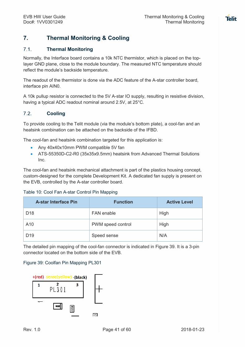
7. Thermal Monitoring & Cooling
Thermal Monitoring
Normally, the Interface board contains a 10k NTC thermistor, which is placed on the top-layer GND plane, close to the module boundary. The measured NTC temperature should reflect the module’s backside temperature.
The readout of the thermistor is done via the ADC feature of the A-star controller board, interface pin AIN0.
A 10k pullup resistor is connected to the 5V A-star IO supply, resulting in resistive division, having a typical ADC readout nominal around 2.5V, at 25°C.
Cooling
To provide cooling to the Telit module (via the module’s bottom plate), a cool-fan and an heatsink combination can be attached on the backside of the IFBD.
The cool-fan and heatsink combination targeted for this application is: • Any 40x40x10mm PWM compatible 5V fan • ATS-55350D-C2-R0 (35x35x9.5mm) heatsink from Advanced Thermal Solutions
Inc.
The cool-fan and heatsink mechanical attachment is part of the plastics housing concept, custom-designed for the complete Development Kit. A dedicated fan supply is present on the EVB, controlled by the A-star controller board.
Table 10: Cool Fan A-star Control Pin Mapping
A-star Interface Pin Function Active Level
D18 FAN enable High
A10 PWM speed control High
D19 Speed sense N/A
The detailed pin mapping of the cool-fan connector is indicated in Figure 39. It is a 3-pin connector located on the bottom side of the EVB.
Figure 39: Coolfan Pin Mapping PL301

EVB HW User Guide Connectors Doc#: 1VV0301249 IO Connectors
Rev. 1.0 Page 42 of 60 2018-01-23
8. Connectors
IO Connectors
Besides the main 120p extension connector, several dedicated IO interface connectors are available. The I/O interface connectors are based on the Samtec 10p pin header connector type: SHF-105-01-L-D-SM-LC, which can be mated with Samtec IDC wire cable FFSD-05-D.
The tables below list the signals available / visible at each header.
Table 11: SO206: ADC
1 VBAT_AUX 2 ADC_IN1
3 GND 4 ADC_IN2
5 GND 6 ADC_IN3
7 GND 8 TGPIO_07
9 1.8V 10 GND
Table 12: SO205: DVI
1 DVI_WAO 2 VBAT_AUX
3 DVI_TX 4 1.8V
5 DVI_RX 6 TGPIO_04
7 DVI_CLK 8 GND
9 REF_CLK 10 GND
Table 13: SO207: I2C
1 VBAT_AUX 2 I2C_SDA
3 1.8V 4 I2C_SCL
5 TGPIO_22 6 GND
7 I2C_SDA_AUX 8 GND
9 I2C_SCL_AUX 10 GND

EVB HW User Guide Connectors Doc#: 1VV0301249 IO Connectors
Rev. 1.0 Page 43 of 60 2018-01-23
Table 14: SO208: SPI
1 SPI_MOSI 2 VBAT_AUX / 1.8V (selected by PL206)
3 SPI_MISO 4 TGPIO_11
5 SPI_CS 6 TGPIO_12
7 SPI_CLK 8 GND
9 GND 10 GND
Table 15: SO211: GPIO1
1 1.8V 2 TGPIO_01
3 TGPIO_02 4 TGPIO_03
5 TGPIO_04 6 TGPIO_05
7 TGPIO_06 8 TGPIO_07
9 TGPIO_08 10 GND
Table 16: SO209: GPIO2
1 VBAT_AUX 2 1.8V
3 TGPIO_09 4 TGPIO_10
5 TGPIO_11 6 TGPIO_12
7 TGPIO_20 8 TGPIO_21
9 TGPIO_22 10 GND

EVB HW User Guide Connectors Doc#: 1VV0301249 120-pin Male B2B Connectors
Rev. 1.0 Page 44 of 60 2018-01-23
120-pin Male B2B Connectors
The interface between IFBD and EVB is implemented via three units of 120p (20p x 6 rows) Samtec SEARAY 1.27mm High Speed/High Density B2B connectors (10mm stack height SEAM/SEAF).
The tables below provide the detailed pin mapping.
The actual pin functionality applied to each pin is determined according to the specific module features and according to the mapping implemented on each specific IFBD.
Signal names and signal functionality are likely to change across platforms.
Refer to the User Guide of the specific IFBD in use for the actual pin mapping and pin description.

EVB HW User Guide Connectors Doc#: 1VV0301249 120-pin Male B2B Connectors
Rev. 1.0 Page 45 of 60 2018-01-23
Table 17: SO501
1 GND 2 GND 3 I2C_SCL_AUX 4 I2C_SDA_AUX 5 GND 6 SGMII_RX_M
7 USB_SS_RX_P 8 GND 9 I2C_SDA 10 TGPIO_06 11 SGMII_TX_M 12 SGMII_RX_P
13 USB_SS_RX_M 14 GND 15 TGPIO_05 16 I2C_SCL 17 SGMII_TX_P 18 GND
19 GND 20 GND 21 VREG_MSME 22 VREG_MSME 23 GND 24 PCIE_RX_P
25 USB_SS_TX_P 26 GND 27 28 29 PCIE_TX_P 30 PCIE_RX_M
31 USB_SS_TX_M 32 GND 33 TGPIO_12 34 SPI_MOSI 35 PCIE_TX_M 36 GND
37 GND 38 39 TGPIO_11 40 TGPIO_04 41 GND 42 PCIE_REFCLK_P
43 SPI_CS 44 TGPIO_02 45 TGPIO_03 46 SPI_MISO 47 48 PCIE_REFCLK_M
49 VAUX/PWRMON 50 VAUX/PWRMON 51 LED_DRV_EN 52 SPI_CLK 53 54
55 TGPIO_08 56 TGPIO_07 57 TGPIO_01 58 TGPIO_09 59 60 CSI2_D0_N
61 TGPIO_21 62 TGPIO_10 63 TGPIO_22 64 TGPIO_20 65 66 CSI2_D0_P
67 VMMC 68 VMMC 69 MMC_CD 70 MMC_DAT3 71 72 CSI2_CLK_N
73 MMC_DAT0 74 MMC_DAT2 75 MMC_CLK 76 MMC_DAT1 77 PCIE_EP_RESET_N 78 CSI2_CLK_P
79 GND 80 GND 81 C107/DSR 82 MMC_CMD 83 PCIE_CLKREQ_N 84 CSI1_D0_N
85 WIFI_SD0_TGPIO15 86 WIFI_SD1_TGPIO16 87 WIFI_SDCMD_TGPIO14 88 WIFI_SDRST_TGPIO13 89 TX_AUX 90 CSI1_D0_P
91 WIFI_SD5_TGPIO24 92 WIFI_SD2_TGPIO17 93 WIFI_SD3_TGPIO18 94 WIFI_SD4_TGPIO23 95 RX_AUX 96 CSI1_D1_N
97 WIFI_SD6_TGPIO25 98 WIFI_SD7_TGPIO26 99 WIFI_SDCLK_TGPIO19 100 WCI_TX 101 WCI_RX 102 CSI1_D1_P
103 C125/RING 104 RFCLK2_QCA 105 WLAN_SLEEP_CLK 106 C105/RTS 107 PCIE_EP_WAKE_N 108 CSI1_D2_N
109 C104/RXD 110 C109/DCD 111 C103/TXD 112 C106/CTS 113 C108/DTR 114 CSI1_D2_P
115 116 117 CSI1_CLK_P 118 CSI1_CLK_N 119 CSI1_D3_P 120 CSI1_D3_N

EVB HW User Guide Connectors Doc#: 1VV0301249 120-pin Male B2B Connectors
Rev. 1.0 Page 46 of 60 2018-01-23
Table 18: SO502
1 GPS_LNA_BIAS 2 GND 3 GPS_LNA_EN 4 MICBIAS 5 GND 6 JACKDET
7 GND 8 GND 9 GND 10 GND 11 GND 12
13 MIC2_MT+ 14 MIC2_MT- 15 GND 16 EAR2_MT- 17 EAR2_MT+ 18
19 GND 20 GND 21 GND 22 GND 23 GND 24 GND
25 MIC1_MT+ 26 MIC1_MT- 27 GND 28 EAR1_MT- 29 EAR1_MT+ 30 GND
31 SPKR_N 32 SPKR_P 33 34 35 36 MIC_VDD
37 GND 38 GND 39 D_MIC_CLK 40 D_MIC_DAT_1 41 GND 42 GND
43 TRXN0 44 GND 45 GND 46 GND 47 GND 48 GND
49 TRXP0 50 GND 51 GND 52 ADC_IN3 53 ADC_IN2 54 ADC_IN1
55 56 57 58 59 60
61 DVI_RX 62 DVI_TX 63 DVI_CLK 64 DVI_WAO 65 REF_CLK 66 GND
67 GND 68 GND 69 GND 70 GND 71 GND 72 eSIM_RST
73 GND 74 GND 75 GND 76 GND 77 SIMVCC1 78 SIMVCC1
79 HSIC_STB 80 HSIC_DATA 81 SIMCLK1 82 SIMIN1 83 SIMIO1 84 SIMRST1
85 HW_KEY 86 VRTC 87 ETH_RST_N 88 ETH_INT_N 89 SIMVCC2 90 SIMVCC2
91 USB_VBUS 92 USB_ID 93 SIMIN2 94 SIMIO2 95 SIMRST2 96 SIMCLK2
97 GND 98 GND 99 MAC_REF_CLK 100 MAC_TXEN_ER 101 MAC_MDIO 102 MAC_RXDV_ER
103 USB_D+ 104 GND 105 MAC_TXD[0] 106 MAC_MDC 107 MAC_RXD[0] 108 MAC_CRS_DV
109 USB_D- 110 GND 111 MAC_TXD[1] 112 MAC_TXD[2] 113 MAC_RXD[1] 114 MAC_RXD[2]
115 GND 116 GND 117 MAC_TX_CLK 118 MAC_TXD[3] 119 MAC_RX_CLK 120 MAC_RXD[3]

EVB HW User Guide Connectors Doc#: 1VV0301249 120-pin Male B2B Connectors
Rev. 1.0 Page 47 of 60 2018-01-23
Table 19: SO503
1 VBATT 2 VBATT 3 VBATT 4 VBATT_PA 5 VBATT_PA 6 VBATT_PA
7 VBATT 8 VBATT 9 VBATT 10 VBATT_PA 11 VBATT_PA 12 VBATT_PA
13 VBATT 14 VBATT 15 VBATT 16 VBATT_PA 17 VBATT_PA 18 VBATT_PA
19 20 21 22 VBATT_PA 23 VBATT_PA 24 VBATT_PA
25 26 27 28 29 30
31 32 33 34 35 36
37 DSI_CLK_P 38 DSI_CLK_N 39 40 41 42
43 DSI_D3_P 44 DSI_D3_N 45 46 47 48
49 DSI_D2_P 50 DSI_D2_N 51 52 53 54
55 DSI_D1_P 56 DSI_D1_N 57 TGPIO_27_TXD_GPS 58 TGPIO_28_RXD_GPS 59 TGPIO_29_RTS_GPS 60 TGPIO_30_CTS_GPS
61 DSI_D0_P 62 DSI_D0_N 63 64 65 66 D8_THERM_ASTAR
67 68 69 70 71 72
73 74 75 76 77 78
79 GND 80 GND 81 GND 82 GND 83 GND 84 GND
85 GND 86 GND 87 GND 88 GND 89 GND 90 GND
91 RESET 92 ON_OFF 93 STAT_LED 94 LED_DRV 95 SW_RDY 96 SHDN
97 GND 98 GND 99 GND 100 GND 101 102
103 GPS_PPS 104 GPS_RFPAON 105 GPS_CLK 106 GND 107 108 JTAG_PS_HOLD
109 GND 110 GND 111 GND 112 GND 113 JTAG_TDI 114 D_MIC_DAT_2
115 JTAG_TMS 116 JTAG_TDO 117 JTAG_TRST 118 JTAG_TCK 119 JTAG_RTCK 120 JTAG_RESOUT
EVB HW User Guide Connectors Doc#: 1VV0301249 Extension Connector
Rev. 1.0 Page 48 of 60 2018-01-23
Extension Connector
As described above, the EVB features can be extended by adding / designing extension cards, which are then plugged into the SO506 connector of the EVB main board.
The detailed pin allocation of the extension connector is shown in the table below.
The actual functionality of each signal is determined by the specific module in use and by the specific extension card. Signal names and signal functionality are likely to change across platforms.
Refer to the relevant extension card HW User Guide.

EVB HW User Guide Connectors Doc#: 1VV0301249 Extension Connector
Rev. 1.0 Page 49 of 60 2018-01-23
Table 20: Extension Connector
1 VBAT_AUX 2 VBAT_AUX 3 DSI_CLK_N 4 DSI_CLK_P 5 DSI_D3_N 6 DSI_D3_P
7 GND 8 GND 9 GPS_PPS 10 WIFI_SDCMD_TGPIO14 11 WCI_RX 12 DSI_D2_N
13 VAUX/PWRMON 14 WIFI_SD4_TGPIO23 15 LED_DRV 16 WIFI_SDCLK_TGPIO19 17 TGPIO_30_CTS_GPS 18 DSI_D2_P
19 1V8 20 WIFI_SD3_TGPIO18 21 LED_DRV_EN 22 WIFI_SD7_TGPIO26 23 DSI_D1_N 24 DSI_D1_P
25 WCI_TX 26 RFCLK2_QCA 27 WIFI_SD2_TGPIO17 28 WIFI_SD5_TGPIO24 29 DSI_D0_N 30 DSI_D0_P
31 I2C_SCL_AUX 32 I2C_SDA_AUX 33 WIFI_SD0_TGPIO15 34 WIFI_SD1_TGPIO16 35 CSI1_CLK_P 36 CSI1_CLK_N
37 I2C_SDA_EXT 38 I2C_SCL_EXT 39 WIFI_SD6_TGPIO25 40 WIFI_SDRST_TGPIO13 41 CSI1_D3_P 42 CSI1_D3_N
43 TGPIO_20 44 TGPIO_01 45 TGPIO_02 46 TGPIO_03 47 CSI1_D2_P 48 CSI1_D2_N
49 TGPIO_21 50 TGPIO_04 51 TGPIO_05 52 TGPIO_06 53 CSI1_D1_P 54 CSI1_D1_N
55 TGPIO_22 56 TGPIO_07 57 TGPIO_08 58 TGPIO_09 59 CSI1_D0_P 60 CSI1_D0_N
61 ETH_INT_N 62 TGPIO_10 63 TGPIO_11 64 TGPIO_12 65 CSI2_CLK_P 66 CSI2_CLK_N
67 ETH_RST_N 68 PCIE_CLKREQ_N 69 PCIE_EP_WAKE_N 70 PCIE_EP_RESET_N 71 CSI2_D0_P 72 CSI2_D0_N
73 MAC_RXDV_ER 74 MAC_MDIO 75 TGPIO_29_RTS_GPS 76 TGPIO_28_RXD_GPS 77 TGPIO_27_TXD_GPS 78 PCIE_REFCLK_M
79 MAC_CRS_DV 80 MAC_MDC 81 WLAN_SLEEP_CLK 82 REF_CLK 83 GND 84 PCIE_REFCLK_P
85 MAC_RXD[3] 86 MAC_TXEN_ER 87 DVI_CLK 88 DVI_WAO 89 PCIE_TX_M 90 GND
91 MAC_RXD[2] 92 MAC_REF_CLK 93 DVI_RX 94 DVI_TX 95 PCIE_TX_P 96 PCIE_RX_M
97 MAC_RX_CLK 98 MAC_TXD[2] 99 SPI_CLK 100 SPI_CS 101 GND 102 PCIE_RX_P
103 MAC_RXD[1] 104 MAC_TX_CLK 105 SPI_MISO 106 SPI_MOSI 107 SGMII_TX_P 108 GND
109 MAC_RXD[0] 110 MAC_TXD[1] 111 GND 112 GND 113 SGMII_TX_M 114 SGMII_RX_P
115 MAC_TXD[3] 116 MAC_TXD[0] 117 USB_EXT_D- 118 USB_EXT_D+ 119 GND 120 SGMII_RX_M

EVB HW User Guide EVB Component Diagram Doc#: 1VV0301249
Rev. 1.0 Page 50 of 60 2018-01-23
9. EVB Component Diagram 9.1.
CS1742E_Placement.pdf
Figure 40: EVB Component Diagram Top View

EVB HW User Guide EVB Component Diagram Doc#: 1VV0301249
Rev. 1.0 Page 51 of 60 2018-01-23
Figure 41: EVB Component Diagram Bottom View

EVB HW User Guide Schematics Doc#: 1VV0301249
Rev. 1.0 Page 52 of 60 2018-01-23
10. Schematics
CS1742E_Schematics.pdf

EVB HW User Guide Schematics Doc#: 1VV0301249
Rev. 1.0 Page 53 of 60 2018-01-23

EVB HW User Guide Schematics Doc#: 1VV0301249
Rev. 1.0 Page 54 of 60 2018-01-23

EVB HW User Guide Schematics Doc#: 1VV0301249
Rev. 1.0 Page 55 of 60 2018-01-23

EVB HW User Guide Schematics Doc#: 1VV0301249
Rev. 1.0 Page 56 of 60 2018-01-23

EVB HW User Guide Safety Recommendations Doc#: 1VV0301249
Rev. 1.0 Page 57 of 60 2018-01-23
11. Safety Recommendations
READ CAREFULLY
Be sure that the use of this product is allowed in your country and in the environment required. The use of this product may be dangerous and must be avoided in the following areas:
• Where it can interfere with other electronic devices in environments such as hospitals, airports, aircrafts, etc.
• Where there is risk of explosion such as gasoline stations, oil refineries, etc.
It is the responsibility of the user to enforce the country regulations and the specific environment regulations.
Do not disassemble the product; any mark of tampering will compromise the warranty validity.
It is recommended following the instructions of the hardware user guides for correct wiring of the product. The product must be supplied with a stabilized voltage source and the wiring conform to the security and fire prevention regulations.
The product must be handled with care, avoiding any contact with the pins because electrostatic discharges may damage the product itself. The same caution must be taken for the SIM, checking carefully the instructions for its use. Do not insert or remove the SIM when the product is in power saving mode.
The system integrator is responsible for the functioning of the final product; therefore, care must be taken of the external components of the module, as well as of any project or installation issue, because of the risk of disturbing the GSM network or external devices or having any impact on safety. Should there be any doubt, please refer to the technical documentation and the regulations in force.
Every module must be equipped with a proper antenna with the specified characteristics. The antenna must be installed with care in order to avoid any interference with other electronic devices and must be installed with the guarantee of a minimum 20 cm distance from a human body. In case this requirement cannot be satisfied, the system integrator must assess the final product against the SAR regulation.
The European Community provides some Directives for electronic equipment introduced on the market. All the relevant information is available on the European Community website:
http://europa.eu.int/comm/enterprise/rtte/dir99-5.htm
The text of the Directive 99/05 regarding telecommunication equipment is available, while the applicable Directives (Low Voltage and EMC) are available at:
http://europa.eu.int/comm/enterprise/rtte/dir99-5.htm

EVB HW User Guide Acronyms Doc#: 1VV0301249
Rev. 1.0 Page 58 of 60 2018-01-23
12. Acronyms
CABC Content Adaptive Backlight Control
CSI Camera serial interface
DSI Display serial interface
EVB Evaluation Board
GPIO General-purpose input/output
IFBD Interface Board
MIPI Mobile Industry Processor Interface
SD Secure digital
SIM Subscriber Identity module
UART Universal asynchronous receiver transmitter
UMTS Universal mobile telecommunications system
USB Universal serial bus
USIF Universal serial interface
WCDMA Wideband code division multiple access

EVB HW User Guide Document History Doc#: 1VV0301249
Rev. 1.0 Page 59 of 60 2018-01-23
13. Document History
Table 21: Document History
Revision Date Changes
1.0 2018-01-23
Minor updates related to new board version (CS1742E)
Added support for numerous product families
Updated to new template
0.9 2016-09-20 Added Class D bypass option
Updated jumpers settings
0.8 2016-09-02 Minor edits
0.7 2016-08-24
Added GPS LNA control description
Several formatting changes
Changed naming convention: from SDK to EVB
0.6 2016-06-06 Fixed typo in Chapter 4 (default jumper setting)
0.5 2016-05-28 Update according to internal review comments
0.4 2016-05-23 Updates for HE922-3GR
Updates for a proper generic EVB description
0.3 2016-02-08 Minor edits
0.2 2016-01-02 Minor edits
0.1 2015-12-16 First draft
