estimates of pulsed electric fields using optical...
TRANSCRIPT

SANDIA REPORT SAND2013-8205 Unlimited Release Printed September 2013
Estimates of Pulsed Electric Fields Using Optical Measurements Timothy M. Flanagan and Gary R. Chantler Prepared by Sandia National Laboratories Albuquerque, New Mexico 87185 and Livermore, California 94550
Sandia National Laboratories is a multi-program laboratory managed and operated by Sandia Corporation, a wholly owned subsidiary of Lockheed Martin Corporation, for the U.S. Department of Energy's National Nuclear Security Administration under contract DE-AC04-94AL85000. Approved for public release; further dissemination unlimited.

2
Issued by Sandia National Laboratories, operated for the United States Department of Energy by Sandia Corporation. NOTICE: This report was prepared as an account of work sponsored by an agency of the United States Government. Neither the United States Government, nor any agency thereof, nor any of their employees, nor any of their contractors, subcontractors, or their employees, make any warranty, express or implied, or assume any legal liability or responsibility for the accuracy, completeness, or usefulness of any information, apparatus, product, or process disclosed, or represent that its use would not infringe privately owned rights. Reference herein to any specific commercial product, process, or service by trade name, trademark, manufacturer, or otherwise, does not necessarily constitute or imply its endorsement, recommendation, or favoring by the United States Government, any agency thereof, or any of their contractors or subcontractors. The views and opinions expressed herein do not necessarily state or reflect those of the United States Government, any agency thereof, or any of their contractors. Printed in the United States of America. This report has been reproduced directly from the best available copy. Available to DOE and DOE contractors from U.S. Department of Energy Office of Scientific and Technical Information P.O. Box 62 Oak Ridge, TN 37831 Telephone: (865) 576-8401 Facsimile: (865) 576-5728 E-Mail: [email protected] Online ordering: http://www.osti.gov/bridge Available to the public from U.S. Department of Commerce National Technical Information Service 5285 Port Royal Rd. Springfield, VA 22161 Telephone: (800) 553-6847 Facsimile: (703) 605-6900 E-Mail: [email protected] Online order: http://www.ntis.gov/help/ordermethods.asp?loc=7-4-0#online

3
SAND2013-8205 Unlimited Release
Printed September 2013
Estimating Pulsed Electric Fields Using Optical
Measurements
Timothy M. Flanagan and Gary R. Chantler Radiation Effects Experimentation
Sandia National Laboratories PO Box 5800
Albuquerque, NM 87185-1167
Abstract
We performed optical electric field measurements ion nanosecond time scales using the electro‐optic crystal beta barium borate (BBO). Tests were based on a preliminary bench top design intended to be a proof‐of‐principle stepping stone towards a modular‐design optical E‐field diagnostic that has no metal in the interrogated environment. The long term goal is to field a modular version of the diagnostic in experiments on large scale x‐ray source facilities, or similarly harsh environments.

4
ACKNOWLEDGEMENTS This work was funded under LDRD Project Number 159299 and Title "Using a Nonlinear Crystal to Optically Measure Pulsed Electric Fields in Radiation Environments".

5
CONTENTS
ACKNOWLEDGEMENTS ............................................................................................................ 4
CONTENTS ............................................................................................................................... 5
INTRODUCTION ....................................................................................................................... 6
EXPERIMENT CONCEPT ............................................................................................................ 7
ELECTRO‐OPTIC CRYSTAL BBO ................................................................................................. 8
EXPERIMENT SETUP ............................................................................................................... 11
LASER ........................................................................................................................................................................ 11
BENCH OPTICS ............................................................................................................................................................. 11
PULSED ELECTRIC FIELD ................................................................................................................................................. 11
DETECTORS ................................................................................................................................................................. 12
MEASUREMENTS ................................................................................................................... 13
CONCLUSIONS AND FUTURE PLANS ....................................................................................... 16
REFERENCES .......................................................................................................................... 17

6
INTRODUCTION Many Radiation Effects Science experiments are designed to provide data that is used for code
validation, which is a critical endeavor in today’s absence of facilities that can simulate the physics
conditions present in weapons environments. Two of the most basic and fundamental quantities the
codes predict in pulsed radiation environments are the time‐varying electric and magnetic fields.
Reliable magnetic field measurements are readily available with B‐dot probes and, under conditions
absent of space charge and gas ionization, it is perfectly reasonable to infer electric field values from
magnetic field measurements. However, separate experimental estimates of electric and magnetic
fields are required to thoroughly test the codes’ predictions. Traditional electric field measurements
have been found to be unreliable. These methods often involve electrical probes with exposed
conductors. The exposed metal becomes a current collector, and the sensor can perturb the E‐field
environment rather than characterize it. Consequently, the majority of validation data is from magnetic
field measurements alone.
The successful development of an optical electric field sensor would make possible a whole new
family of data to be used for code validation. Measuring electric field in this manner is advantageous
because it need not introduce any metal into the environment under measurement. Using a wide
variety of electro‐optic crystals, electric fields have been optically measured in frequency regimes
ranging from dc [1, 2] to the microwave spectrum in both a CW [3] and a pulsed [4] configuration.
Application environments studied include electron beams [5], radiation detectors [6], electrical
discharges [7] and electrical power [8, 9].
In this report, we present preliminary optical measurements of pulsed electric field using a laser,
some simple optical components, photo diode detectors, and a crystal of beta barium borate (BBO). The
crystal structure of BBO is such that it has no center of symmetry, and thus supports a linear electro‐
optic effect, also known as the Pockels effect. While BBO is routinely used for optical switching and
second harmonic generation [10] in the visible and UV spectrum, we are aware of only one recent
application of BBO for measurements of electric field [11].

7
EXPERIMENT CONCEPT The electric field measurement is based on the Pockels effect: the speed of light in certain anisotropic
crystals changes linearly with an externally applied E‐field. Because the crystal is anisotropic, its index of
refraction is not described by a single number but rather by a tensor that is indicative of the crystalline
structure. Thus, the speed of light in the crystal generally depends on the direction of propagation.
Additionally, if the crystal’s atomic structure has no center of symmetry, then the crystal’s refraction
indices change in linear proportion to an external electric field. This also depends on the orientation of
the external field with respect to the crystal axes. We will refer to a crystal such as this as electro‐optic.
Polarized light, such as a laser beam, propagating through an electro‐optic crystal will change in
proportion to an external electric field. The E‐field‐induced changes in refractive index are typically too
small to significantly alter the laser beam’s direction. However, the changes are large enough that the
laser light’s high‐frequency (1015 Hz) electric field components (polarization) undergo a relative phase
shift due to the low‐frequency E‐field applied to the crystal (i.e., polarization components travel at
different speeds). Due to the phase shift, the polarization state of light exiting the crystal changes, which
can be detected with polarizers and a photodiode. The external electric field modulates the polarization
state of the beam exiting the crystal, and a polarizer can be used to transform this into a beam‐intensity
modulation. By measuring the output laser intensity with a photodiode, the E‐field pulse strength can be
obtained using known properties of the crystal and laser.
In this work, the sensor’s basic components consist of the electro‐optic crystal, a freely propagating
continuous‐wave laser, photodiode detectors, and a high extinction polarizing beam splitter with two
usable output beams. The field under measurement is provided by coupling the output of a pulser (kV
pulse amplitudes and ns pulse widths) to parallel plates. The crystal is mounted between the plates.
The setup is appropriate for proof‐of‐principle measurements, since it consists of bench‐top instruments
and optical components that are easily adjusted and interchanged. The set up could be changed a
number of ways to utilize a packaged, more modular sensor. For instance, fielding in a harsh
environment where an optics table is not practical may require laser light sent over fiber optics rather
than an open beam. The sensor’s final design could package the crystal and polarizers in a fixed relative
orientation inside a protective dielectric housing.

8
ELECTRO-OPTIC CRYSTAL BBO
We chose beta barium borate (‐BaB2O4), also known as BBO, as the electro‐optic crystal to use in this
sensor. We know of no previous work where BBO was used in an optical E‐field sensor at nanosecond
time scales, and only one recent work where it was used at all [11]. While there are many commercially
available crystals that demonstrate the Pockels effect, BBO has many properties [12] that are
particularly well‐suited for measurement of pulsed electric fields:
1. BBO is known for its fast electro‐optic response and its high optical damage threshold [13, 14].
2. BBO has a very weak acousto‐optic and magneto‐optic response which distinguishes it from
other well‐known crystals that are often used for optical switching, such as LiNbO3 and KDP.
When applying an external pulsed E‐field, LiNbO3 can be dominated by acousto‐optic ringing
after the E‐field pulse ends or while it is still present. KDP has a magneto‐optic response that
will compete with the desired electro‐optic response in a pulsed field environment. This could
complicate the diagnostic since the laser’s overall polarization would be rotated by the magnetic
field while its polarization components are simultaneously driven out of phase by the electric
field.
3. BBO has only one non‐trivial electro‐optic coefficient that is of appreciable magnitude,
2.5 pm/V [15, 16]. Only fields in the crystal’s x‐y plane can change its
index of refraction (the optical axis is the z axis). This can help reduce analysis complications
when making measurements in an environment where the E‐field direction is not exactly
known.
4. Because it is uniaxial, BBO can be used in a configuration where a laser beam can propagate
along an axis that has no birefringence in the absence of an external E‐field. This allows the
beam to propagate through the crystal with its polarization state unperturbed in the absence of
field.
5. The easiest configuration to field BBO is with the E‐field perpendicular to the laser beam. For a
bench top test setup where a field is purposely applied, one can just place the crystal between
parallel plates and have the laser beam propagate between the plates. No transparent
electrodes are necessary to introduce your electric field.
6. BBO has a dc dielectric constant that is quite low ( = 6.7, ), so external fields can more
efficiently couple inside the crystal. Many other common electro‐optic crystals have dielectric
constants ranging from 30 to 100 [17].
The most common formalism used to study how optical properties of electro‐optic crystals change
under an external electric field is the optical indicatrix or the index ellipsoid [18, 19]. It will not be
reproduced here, except to say that it is an ellipsoid in the space of the electric displacement that
represents surfaces of constant energy density stored in the crystal’s electric field , 12 ⋅ .
In a BBO crystal’s principle axis coordinate system without an external electric field, this ellipse is
represented by
1

9
where and are the crystal’s ordinary and extraordinary index of refraction. If an electromagnetic
wave propagates along the crystal’s z‐axis, its polarization components along x and y both move at
speed ⁄ .
When the BBO crystal is immersed in an external electric field , , the index ellipsoid changes according to
2 1.
This is clearly complicated since the principle axes have been rotated in a way that is electric field
dependent. But if one chooses the field to be entirely along ( 0) then the crystal’s principle axes rotate to be ±45˚ from the axis in the ‐plane, with no field dependence, and the ‐projection of
the index ellipsoid goes form circular to slightly elliptical. Even better, if one chooses the field to be
entirely along ( 0) then the crystal’s principle axes do not change at all, but the projection on the ‐plane reaches the same ellipticity. This latter set up is used in our experimental setup, where the
equation for the index ellipsoid then becomes
1 11.
Usually will be on the order 10‐8 for fields measured here, and still extremely small for larger
external fields. Compared to1⁄ , which is of order unity, the electro‐optic index change is extremely
small and we can write it as simply a small perturbation.
12 1
2
If the crystal is long enough and the optics sensitive enough this birefringence can be measured by
determining the output polarization of a laser beam exiting the crystal.
Because we want to measure fields that are as low as possible without complicating the experiment, we
purchased a very long crystal. The relative phase retardation between a ‐propogating beam’s two
polarization directions ( , ) is proportional to the length of the crystal and is written as
The crystal dimensions are 6mm x 6mm x 25 mm where the long
dimension is along the optic axis ( ). A photo of the crystal in its Delrin mount along with an artist’s
rendering is shown in Figure 1.

10
Figure 1: BBO photo (left) and illustration (right). The BBO crystal is AR coated for 532 nm at its entrance and exit faces along the 25‐mm optical axis = = 1.55. Light traveling along the z‐axis ( = 532 nm) is polarized along the 6‐mm X and Y axes, with refraction indices of = = = 1.67. When an electric field is applied along the Y direction, the principles axes of
BBO’s index tensor remain unchanged, but and increase and decrease by , respectively. The polarized
wave slows down, the polarized wave speeds up, and the resulting phase retardation
( = 25 mm) changes the polarization state of the exiting laser beam. The phase retardation is measured by separating the waves with a polarizing beam splitter and measuring their intensity. The relation to is then simple.

11
EXPERIMENT SETUP
LaserThe fields we seek to measure will only produce phase retardations on order of 0 to 10˚. Thus, the
output beams will only increase and decrease their intensity by a small amount. If these small changes
are to be easily detected on fast time scales, we should be careful to choose a laser that will not cloud
these measurements with random noise in its output intensity. We used a diode‐pumped solid state
laser Verdi V6 from Coherent due to its attractive specification in RMS noise of < 0.02% up to 1 GHz and
its single‐frequency line output at 532‐nm.
BenchOpticsWe set up the experiment so that circularly polarized light enters the crystal. Because the refraction indices increase and decrease by the same amount when a field is applied along the crystal’s ‐axis, it makes sense to measure two output beams of orthogonal polarization. Further, it makes sense to set up the experiment so the two output beams have equal intensity in the absence of an external electric field. One beam’s intensity will increase and the other will decrease by a similar amount. In principle, this gives a balanced measurement where the sum of the two beam intensities should be the same at any point in time regardless of the applied field.
Figure 2: Optics set up. A 6 Watt green laser exits the laser head and immediately is attenuated to levels suitable for the photo diodes using a half‐wave plate and a polarizing beam splitter. A Glan‐laser polarizer is used to further improve purity of the linearly polarized beam. A zero order quarter‐wave bias plate is used so that circularly polarized light enters the BBO crystal. The beam exiting the crystal goes through a specialty high‐extinction polarizing beam splitter with two orthogonally polarized output beams with extinctions that do not exceed 10‐5. Each beam is incident on a silicon photo receiver giving two balanced intensity measurements.
PulsedElectricFieldThe pulser used is from Grant Applied Physics and has a negative polarity output variable between 0 and
2 kV with pulse widths of 1, 2, 3, 4, 5 and 6 ns. This is coupled to two parallel aluminum plates that are 6
x 6 in2 and separated by 3.1 cm. Thus, the electric field applied in the volume between the plates is a
maximum of 650 V/cm. Due to stray resistance and inductance, and because the plates are not
impedance matched to the pulser, the pulser output couples to the plates in such a way that reflections
ring back and forth between them; the applied voltage looks like a noisy damped sinusoid. While this is
not ideal, it is acceptable for our purposes because the optical detectors can reproduce the temporal
12
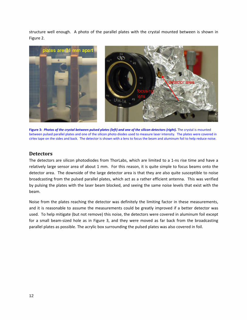
structure well enough. A photo of the parallel plates with the crystal mounted between is shown in
Figure 2.
Figure 3: Photos of the crystal between pulsed plates (left) and one of the silicon detectors (right). The crystal is mounted between pulsed parallel plates and one of the silicon photo diodes used to measure laser intensity. The plates were covered in cirlex tape on the sides and back. The detector is shown with a lens to focus the beam and aluminum foil to help reduce noise.
DetectorsThe detectors are silicon photodiodes from ThorLabs, which are limited to a 1‐ns rise time and have a
relatively large sensor area of about 1 mm. For this reason, it is quite simple to focus beams onto the
detector area. The downside of the large detector area is that they are also quite susceptible to noise
broadcasting from the pulsed parallel plates, which act as a rather efficient antenna. This was verified
by pulsing the plates with the laser beam blocked, and seeing the same noise levels that exist with the
beam.
Noise from the plates reaching the detector was definitely the limiting factor in these measurements,
and it is reasonable to assume the measurements could be greatly improved if a better detector was
used. To help mitigate (but not remove) this noise, the detectors were covered in aluminum foil except
for a small beam‐sized hole as in Figure 3, and they were moved as far back from the broadcasting
parallel plates as possible. The acrylic box surrounding the pulsed plates was also covered in foil.

13
MEASUREMENTS Measurements demonstrate that the electric field applied to the plates can be tracked in time via an
optical measurement. Figure 4 shows the photo receiver signals for the two orthogonal output beams
as a function of time. These are labeled ‘0 deg detector’ and ‘45 deg detector’, referring to the locations
of each detector relative to the laser entering the beam splitting Glan‐Laser polarizer. Before the pulse
output, it is clear in Figure 4 that the two optical detector intensities are very low noise and balanced in
the time interval preceding ‐10 ns. The noise level increases greatly when the pulser starts for reasons
described earlier. However, there is still sufficient signal‐to‐noise to demonstrate that the experiment
works as designed. Each orthogonally polarized beam increases/decreases by very similar amounts
throughout the time history. Further, the structure of the signal is similar to the pulse monitor pickoff
signal.
Figure 4: The pulse monitor and the two balanced optical measurements. The black curve on the bottom (left abscissa) is an external 20x attenuated pickoff of the pulser output that goes to the parallel plates. In these data, the pulser was set to output 1.9 kV for 6 ns. This time period is shown with the red arrow. The blue arrow indicates the rest of the time series where the pulser output reflects back and forth between the pulser and the plates. The red and green curves on the top (right abscissa) are the intensity measurements of the two silicon photo diodes. Within limits of noise and the apparent misalignment in time due to the different detector distances from the BBO, the two optical measurements look balanced as intended.
While the optical signals do appear to be tracking the electric field between the plates, there is a small
difference aside from the obvious noise issues. The pulse monitor returns to zero as the pulse dissipates
while the optical signals return to a small dc offset relative to the pre‐pulse intensity. The offset appears
to be equal and opposite for each orthogonal polarization. While it is not known for sure why this
occurs, it is reasonable to suspect that it is a small residual stress in the BBO crystal that is changing each
refraction index by an equal and opposite amount (i.e., an acousto‐optic effect.) Further study of this
would be important in future measurements if this setup were used to interrogate an unknown electric
0.00
0.05
0.10
0.15
0.20
0.25
‐2
‐1
0
1
2
3
4
5
‐20 0 20 40 60 80 100 120 140 160
pulse monitor0 deg detector45 deg detector
time (ns)
photo diode detectors (V)
puls
erm
onito
r (
kV)
intended output pulse
2kV, 6 ns everything else is reflections between pulser and parallel plates
detectors seem to pick up reflections in a way that is qualitatively the way the set up is designed.
14
field, but it is encouraging that it does not overwhelm the desired signal even at the modest fields
applied in this experiment.
It is tempting to use these data to estimate an electric field as a function of time. This is analytically a
simple task, and is reasonable to do with the stated caveats that: 1) noise is an issue in this setup, 2)
there appears to be some longer time scale, though balanced, residual stress in the crystal that is
introducing another source of birefringence and 3) the field coupling from the pulser to the plate is not
ideal and 4) we do not know exactly how much of the applied field penetrates the crystal. All of these
caveats could be reasonably mitigated in future tests. Setting caveats aside, the electric field is obtained
from the intensity measurements simply by solving the following two equations for the field induced
phase retardation , 12 1 sin 2 1
2 1 sin 2
where Is and Ip are simply the intensity measurements shown in Figure 4. For small , this can be accurately approximated as /2 ⁄ and then related to the electric field inside the
crystal by .
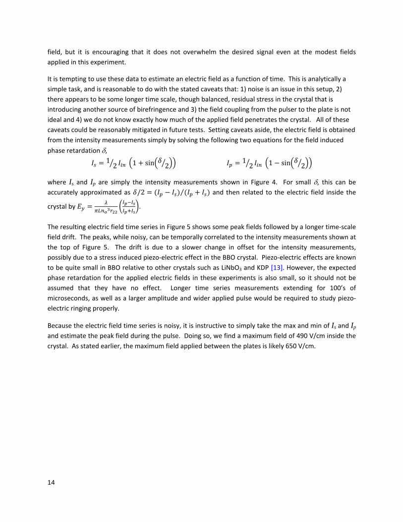
The resulting electric field time series in Figure 5 shows some peak fields followed by a longer time‐scale
field drift. The peaks, while noisy, can be temporally correlated to the intensity measurements shown at
the top of Figure 5. The drift is due to a slower change in offset for the intensity measurements,
possibly due to a stress induced piezo‐electric effect in the BBO crystal. Piezo‐electric effects are known
to be quite small in BBO relative to other crystals such as LiNbO3 and KDP [13]. However, the expected
phase retardation for the applied electric fields in these experiments is also small, so it should not be
assumed that they have no effect. Longer time series measurements extending for 100’s of
microseconds, as well as a larger amplitude and wider applied pulse would be required to study piezo‐
electric ringing properly.
Because the electric field time series is noisy, it is instructive to simply take the max and min of Is and Ip
and estimate the peak field during the pulse. Doing so, we find a maximum field of 490 V/cm inside the
crystal. As stated earlier, the maximum field applied between the plates is likely 650 V/cm.

15
Figure 5: Electric field estimate inside the crystal as a function of time. There is an initial peak near 450 V/cm that is reasonable based on the pulse amplitude applied to the plates (650 V/cm). There is also an apparently artificial offset late in
time that is surmised to be due to residual stress in the crystal. By simply takes the min and max of Ip and Is, .19 and .16, one finds an electric field of 490 V/cm. The measurement is greatly influenced by noise coupling from the pulsed plates to the detectors.
0.00
0.05
0.10
0.15
0.20
0.25
‐500
0
500
1000
1500
‐20 0 20 40 60 80 100 120 140 160
E_field (V/cm)0 deg detector45 deg detector
time (ns)
photo diodedetecto
rs (V)
E y(V/cm)

16
CONCLUSIONS AND FUTURE PLANS We have demonstrated that an electric field estimate can be done optically on nanosecond time scales
using a crystal of beta barium borate (BBO). Further study could result in a reliable electric field sensor
that is free of environment perturbing metal and can track a field with an arbitrary time dependence on
nanosecond time scales. Further development of a sensor that is more practical to use would require
coupling to fiber optics, reducing detector noise, and packaging the crystal and polarizing optics in a
module that could quickly be installed and operated in a harsh environment, such as a pulsed power
facility.
Future plans to improve bench top tests include using a much faster and lower noise detector element
made of indium gallium arsenide. Also, applying the field using an impedance matched strip line would
allow applying any waveform one would like without having to worry about reflections. This could allow
characterization of the BBO electro‐optic response over a wide range of frequencies and field
amplitudes, from DC to arbitrary pulses, to sinusoids. Temperature dependence of the refraction
indices would also be important, but previous studies have shown it to be quite low [12]. Also, material
characterizations and testing of functionality in a radiation environment would be the ultimate test of
utility of this sensor as a supplemental E‐field diagnostic in code validation experiments. This
environment is unknown for all but the most common electro‐optic materials, such as KDP [20‐22].

17
REFERENCES [1] G.A. Massey, D.C. Erickson and R.A. Kadlec, “Electromagnetic field components: their
measurement using linear electrooptic and magnetooptic effects,” Appl. Opt. 14, 2712‐2719 (1975).
[2] S.R.M. Robertson and A.J. Rogers, “Measurement of DC electric fields using the electro‐optic effect,” IEE Proc. 132, pp. 195‐198 (1985).
[3] J. Chang, C.N. Vittitoe, B.T. Neyer and W.P. Ballard, "An electrooptical technique for intense microwave measurements", J. Appl. Phys. 57 (11), 1 June (1985).
[4] N. Kuwabara et al., "Development and analysis of electric field sensor using LiNbO3 optical modulator," IEEE Trans. Electrom. Compat. 34, 391 (1992).
[5] M.A. Brubaker and C.P. Yakmymshyn, "Pockels cell voltage probe for noninvasive electron beam measurements," Appl. Opt. 39, 1164‐1167 (2000).
[6] P. De Antonis, E.J. Morton and F.J.W. Podd, "Infra‐red microscopy of Cd(Zn)Te radiation detectors revealing their internal electric field structure under bias," IEEE Trans. Nucl. Sci. 43, 1487‐1490 (1996).
[7] Y. Fukui, K. Okumura, H. Moritake, and Y. Murooka, "A typical noiseless Pockels E field sensor," Rev. Sci. Instrum. 81, 114701 (2010).
[8] M. Passard, C. Barthod, M. Fortin, C. Galez, and J. Bouillot, "Optimization of an optical device for low frequency electric field measurement," Proc. of SPIE 4074, (2000).
[9] Yongqian Li, Changsheng Li, and Toshihiko Yoshino, "Optical electric‐power‐sensing system using Faraday and Pockels cells," Applied Optics 40, 31 (2001).
[10] G. Palmer, M. Siegel, A. Steinmann, and U. Morgner, "Microjoule pulses from a passively mode‐locked Yb:KY(WO4)2 thin‐disk oscillator with cavity dumping," Optics Lett. 32, No. 11 (2007).
[11] Rong Zeng, Xiaoli Shen, Changsheng Li, and Bo Wang, "Optical electric field sensor using single ‐BaB2O4 crystal", Proc. of SPIE 8421, 84212 (2012).
[12] D. Eimerl, L. Davis, and S. Velsko, "Optical, mechanical, and thermal properties of barium borate," J. Appl. Phys. 62 (5) (1987).
[13] G.D. Goodno et al., “Investigation of ‐BaB2O4 as a Q switch for high power applications,” Appl. Phys. Lett. 66 (13), 1575‐1577 (1995).
[14] H. Nakatani, W.R. Bosenberg, L.K. Cheng, and C.L. Tang, "Laser‐induced damage in beta‐barium borate," Appl. Phys. Lett. 53 (26) (1988).
[15] Chris A. Ebbers, "Linear electro‐optic effect in ‐BaB2O4 ," Appl. Phys. Lett. 52 (23) (1988). [16] H. Nakatani, W. Bosenberg, L.K. Cheng, and C.L. Tang, "Linear electrooptic effect in barium
metaborate," Appl. Phys. Lett. 52 (16) (1988). [17] F. Agullo‐Lopez, J. Manuel Cabrera and F. Agullo‐Rueda in Electrooptics Phenomena, Materials and
Applications, Academic Press Inc., San Diego (1994). [18] I.P. Kaminow in An Introduction to Electrooptic Devices, Academic Press Inc., NewYork (1974). [19] R.W. Boyd in Nonlinear Optics, Elsevier Inc., San Diego (2008). [20] E. Dieguez et al., "Optical absorption and luminescence induced by x rays in KDP, DKDP, and ADP,"
J. Chem. Phys. 8, (8), 3369 (1984). [21] K. Simmons‐Potter, “Transient Radiation Effects in D.O.I Optical Materials: KD*P,” SAND98‐1576
(1998). [22] R.A. Negres, C.K. Saw, and S.G. Demos, "Interactions between X‐ray induced transient defects and
pre‐existing damage precursors in DKDP crystals," Proc. of SPIE 7132 713212 (2008).

18
DISTRIBUTION
1 MS 0425 S.C. Jones 0245 1 MS 1152 K.L. Cartwright 01352 1 MS 1152 C.D. Turner 01352 1 MS 1159 J.W. Bryson 01344 1 MS 1159 B.P. Fox 01344 1 MS 1159 N.W. Moore 01344 1 MS 1159 J.D. Serrano 01344 1 MS 1159 A.L. McCourt 01344 1 MS 1167 G.R. Chantler 01343 1 MS 1167 T.M. Flanagan 01343 1 MS 1167 E.F. Hartman 01343 1 MS 1167 K.M. Horn 01343 1 MS 1167 M.L.McLain 01343 1 MS 1167 T.A. Zarick 01343 1 MS 1167 R.R. Romero 01343 1 MS 1167 T.J. Sheridan 01343 1 MS 1168 B.V. Oliver 01340 1 MS 1179 L.J. Lorence 01341 1 MS 1179 W.C. Fan 01341 1 MS 1202 C.A. Coverdale 05945 1 MS 0899 Technical Library 9536 (electronic copy) 1 MS 0359 D. Chavez, LDRD Office 7911