eos/esd manufacturing symposium in germany · tel: +1-315-339-6937 • fax: ... this tutorial...
TRANSCRIPT
1
EOS/ESD Manufacturing Symposium in Germany November 6-9, 2018
NH Collection Dresden Altmark,
An der Kreuzkirche 2, D–01067 Dresden, Germany
The German ESD FORUM e.V. and the EOS/ESD Association, Inc. are working together to present the 3rd European EOS/ESD Manufacturing Symposium in Dresden, Germany. The collaboration between both organizations focuses on ESD protection issues during handling, assembly, and transport. Register today!
November 6-7: Tutorials
November 8-9: Symposium and Exhibition
www.esda.org www.esdforum.de
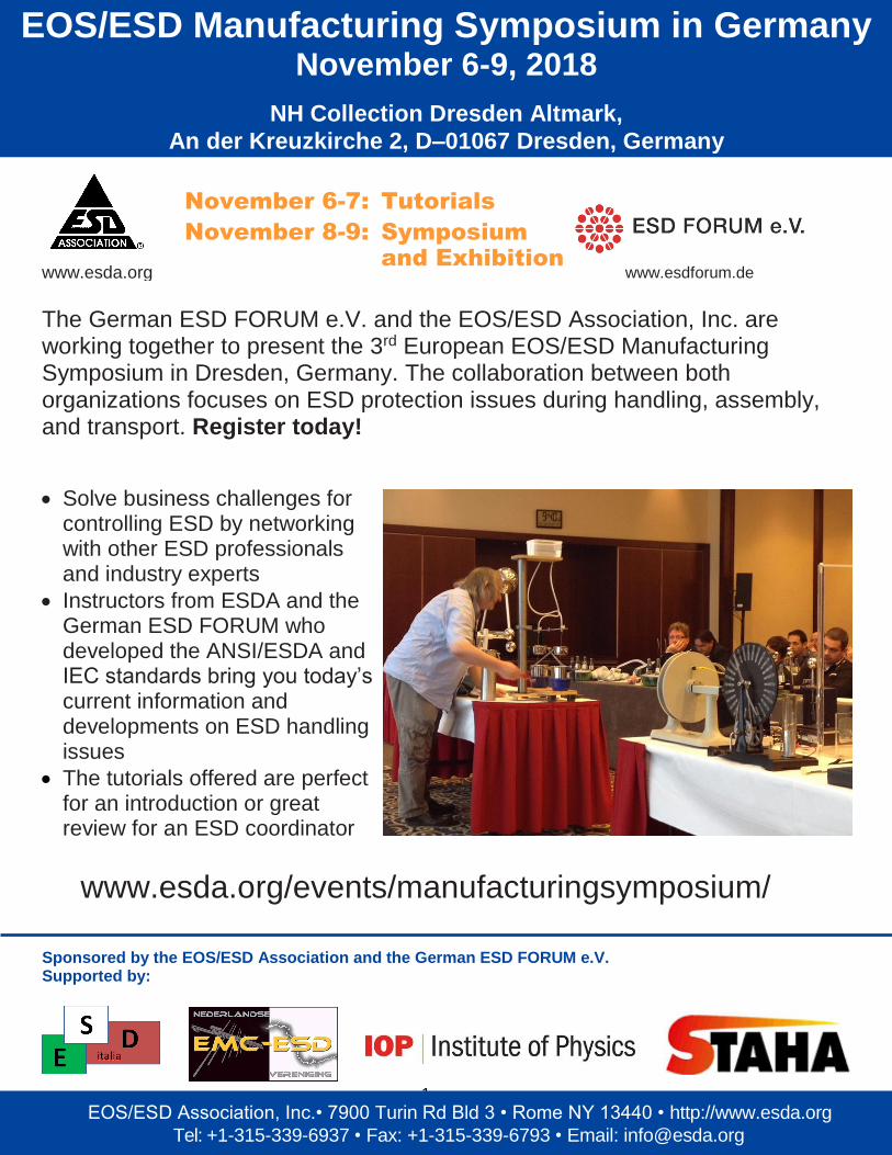
Solve business challenges for controlling ESD by networking with other ESD professionals and industry experts
Instructors from ESDA and the German ESD FORUM who developed the ANSI/ESDA and IEC standards bring you today’s current information and developments on ESD handling issues
The tutorials offered are perfect for an introduction or great review for an ESD coordinator
www.esda.org/events/manufacturingsymposium/
EOS/ESD Association, Inc.• 7900 Turin Rd Bld 3 • Rome NY 13440 • http://www.esda.org
Tel: +1-315-339-6937 • Fax: +1-315-339-6793 • Email: [email protected]
Sponsored by the EOS/ESD Association and the German ESD FORUM e.V. Supported by:
2
EOS/ESD Manufacturing Symposium in Germany Tutorials
ANSI/ESD S20.20 – Process Design Overview TUESDAY, NOVEMBER 6, 2018 • 9:00 AM – 5:00 PM
Instructor: Wolfgang Stadler, Intel Deutschland GmbH
This overview provides instruction on designing and implementing an ESD control program based on ANSI/ESD S20.20.
The course provides participants with the tools and techniques to help with the selection of the ESD controls that are appropriate for the devices to be handled.
The following topics are covered:
ANSI/ESD S20.20 Administrative Requirements
Grounding/Bonding Systems
Personal Grounding
ESD Controls for the EPA
Packaging Requirements
Introduction to Physical Failure Analysis TUESDAY, NOVEMBER 6, 2018 • 9:00 AM – 12:30 PM
Instructor: Pit Jacob, Empa Duebendorf, Electronics & Reliability Center
This tutorial introduces into modern methods of physical failure analysis and failure anamnesis. While failure analysis starts from the device level, failure anamnesis is a top-down approach, starting at a system level. In failure analysis, the first focus is given on failure localization, where methods like photon emission microscopy, OBIRCH (Optical Beam Induced Resistivity CHange) and further localization methods are used as a non-destructive localization approach. Specific destructive preparations and inspections by chemical treatment, FIB (Focused Ion Beam) and SEM (Scanning Electron Microscopy) follow in order to deliver the failure signature, giving important information for failure anamnesis about possible failure scenarios and root causes.
In parallel, failure anamnesis starts investigations on the system level. Here we focus on the failure history and statistics. A very important step of anamnesis is to analyze the circuitry environment of the failed device. Operation-induced ESD may apply in moving systems or hidden inductive components may cause inductive pulses when suffering switching. Also sudden load changes of inductive components within the circuitry environment or coupling of RF into a circuitry may cause ESD-like damage on device level.
What Information Needs to be Exchanged for Potential EOS Problem TUESDAY, NOVEMBER 6, 2018 • 1:30 PM – 5:00 PM
Instructor: Reinhold Gaertner, Infineon Technologies
EOS-like damages represent a significant percentage of components returned by the OEM’s to tier1 and semiconductor manufacturers for comprehensive failure analysis in the automotive industry. There is generally a requirement from the OEM to conduct a detailed investigation to determine the root cause of the failure; however, commonly this cannot be done due to missing information and poor communications but blocks a lot of capacity. This tutorial presents information based on case studies why it is not possible to find the root cause for an EOS-like damage without an information sharing between all tier levels. Based on the new guideline (to be published by WG27) a two level support will be introduced based on an information sharing between the OEM, tier1 and semiconductor manufacturers that can lead to a higher chance to identify the root cause of the damage and allows to focus on the important topics.
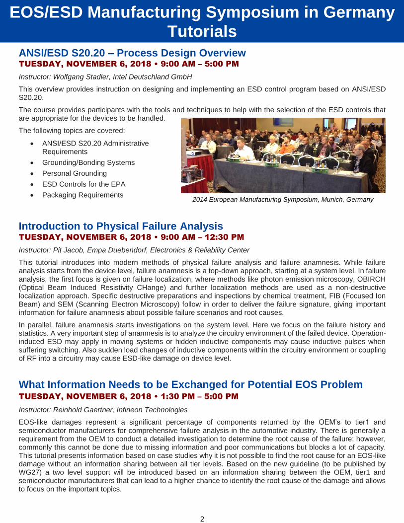
2014 European Manufacturing Symposium, Munich, Germany
3
EOS/ESD Manufacturing Symposium in Germany Tutorials
Basics of ESD Process Assessment (FC390) WEDNESDAY, NOVEMBER 7, 2018 • 9:00 AM – 5:00 PM
Instructors: Reinhold Gaertner, Infineon Technologies; Wolfgang Stadler, Intel Deutschland GmbH
This tutorial gives an introduction to the approach and measurement methodologies for ESD process assessment and ESD risk analysis in typical production processes in semiconductor, printed-circuit board (PCB), and electronic system manufacturing industries. It summarizes the relevant physical parameters (e.g., resistance, charge, electric fields, capacitances, resistances, discharge currents, and ESD event detection by EMI) and discusses their influence on the ESD risks caused by charged personnel, charged devices and boards, and ungrounded conductors.
Measurement techniques are explained in detail together with their limitations for the different process steps and strategies for an efficient ESD risk assessment. The application of those measurement techniques to assess possible ESD risks and to solve ESD problems are explained using theoretical and real-world case studies from each of the processes mentioned above.
Examples of possible mitigation strategies are discussed with the attendees. The tutorial includes practical demonstrations and a hands-on session for the attendees to get experience and learn pitfalls of the most important measurement techniques used in ESD process assessment.
ESD Basics WEDNESDAY, NOVEMBER 7, 2018 • 9:00 AM – 12:30 PM
Instructor: Toni Viheriakoski, Cascade Metrology
This talk will discuss the fundamental causes of ESD and its control. It includes how ESD impacts industry, with brief explanations of charge generation, field measurement, the role of capacitance and voltage, charge measurement, and charge decay. Device failure mechanisms, including the respective test models like Human Body Model or Charged Device Model, will also be explained. The tutorial will discuss how to protect ESD sensitive devices and assemblies, give definitions of an Electrostatic Protected Area (EPA), and show how to assess the risk in an automated production line.
Packaging of Electrostatic Sensitive Devices (ESDS) in Electrostatic Protected Areas (EPA’s) and in Electrostatic Unprotected Areas (UPA’s) WEDNESDAY, NOVEMBER 7, 2018 • 1:30 PM – 3:00 PM
Instructor: Rainer Pfeifle, Wolfgang Warmbier GmbH & Co. KG
Packaging is necessary to protect electrostatic sensitive devices (ESDS) from physical and environmental damage during manufacture, transportation and storage. Additionally, packaging for ESDS should also prevent damage from electrostatic discharges and fields.
This tutorial will explain the relevant aspects for a classification of the properties of ESD packaging based on the valid IEC standard IEC 61340-5-3 and ANSI/ESD S541 for usage in an EPA and in UPA’s. Qualification and verification measurements will be explained and demonstrated during the tutorial. Examples of common packaging items like bags, corrugated cardboard boxes, tote boxes, vacuum formed trays and special packaging systems will be discussed and shown.
This short tutorial is intended to help the participants to decide which packaging is optimal solution to protect their ESDS from ESD events in their facility and when shipped to customers.
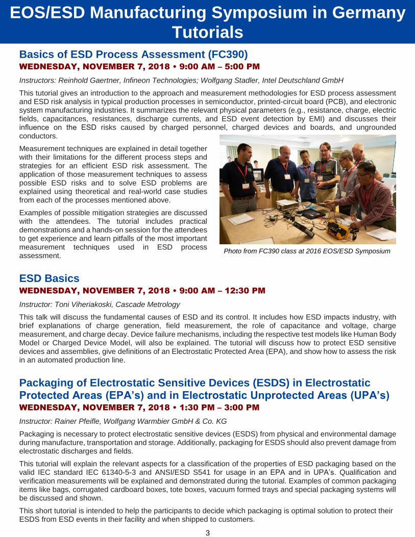
Photo from FC390 class at 2016 EOS/ESD Symposium
4
EOS/ESD Manufacturing Symposium in Germany Tutorials
ESD and Reliability Estimations WEDNESDAY, NOVEMBER 7, 2018 • 3:30 PM – 5:00 PM
Instructor: Armin Gottschalk, IQZG Consulting
Key issue: are the conventional reliability theory and models appropriate to ESD?
Reliability parameters will be explained and its application how failure rates are to be calculated with respect to confidence levels and also under aspects of acceleration factors based on e.g. Arrhenius.
Furthermore relation on test times, e.g. life test time and number of required test specimens are explained.
Contents:
Introduction to Reliability
Reliability Parameters, Exponential and Weibull Distribution
Estimation of Acceleration Factors: Arrhenius, Peck, Lawson, Coffin-Manson
Test Time and Number of Test Specimen
Summary
About the Instructors
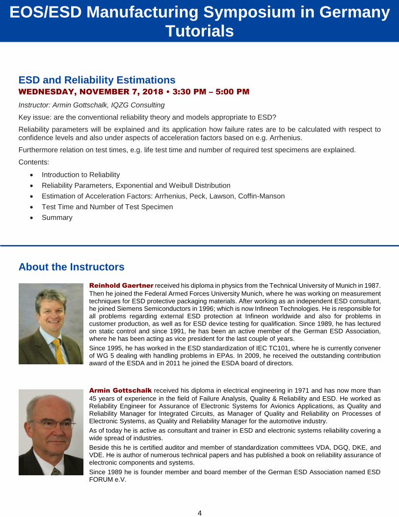
Reinhold Gaertner received his diploma in physics from the Technical University of Munich in 1987.
Then he joined the Federal Armed Forces University Munich, where he was working on measurement techniques for ESD protective packaging materials. After working as an independent ESD consultant, he joined Siemens Semiconductors in 1996; which is now Infineon Technologies. He is responsible for all problems regarding external ESD protection at Infineon worldwide and also for problems in customer production, as well as for ESD device testing for qualification. Since 1989, he has lectured on static control and since 1991, he has been an active member of the German ESD Association, where he has been acting as vice president for the last couple of years.
Since 1995, he has worked in the ESD standardization of IEC TC101, where he is currently convener of WG 5 dealing with handling problems in EPAs. In 2009, he received the outstanding contribution award of the ESDA and in 2011 he joined the ESDA board of directors.
Armin Gottschalk received his diploma in electrical engineering in 1971 and has now more than
45 years of experience in the field of Failure Analysis, Quality & Reliability and ESD. He worked as Reliability Engineer for Assurance of Electronic Systems for Avionics Applications, as Quality and Reliability Manager for Integrated Circuits, as Manager of Quality and Reliability on Processes of Electronic Systems, as Quality and Reliability Manager for the automotive industry.
As of today he is active as consultant and trainer in ESD and electronic systems reliability covering a wide spread of industries.
Beside this he is certified auditor and member of standardization committees VDA, DGQ, DKE, and VDE. He is author of numerous technical papers and has published a book on reliability assurance of electronic components and systems.
Since 1989 he is founder member and board member of the German ESD Association named ESD FORUM e.V.

5
EOS/ESD Manufacturing Symposium in Germany Tutorials
Peter Jacob started his professional work in 1981 after studying Technical Physics in Munich as a
failure analysis expert in IBM semiconductor plant Boeblingen until 1992. After a short period at Hitachi Scientific Instruments, where he was responsible for electron microscopy configurations and customer trainings, he joined ETH Zurich/ Empa as a senior expert for failure analysis on micro- and power-electronics from device to system level. In parallel to this work, in 1995 he joined to Swatch Group – EM Microelectronic Marin as a principal F/A engineer.
Jacob has authored more than 60 contributed and invited papers including two ESREF Best Papers and an ISTFA outstanding poster award. He volunteers in the German ESD FORUM, EDFAS and EuFANet. In 2007 he was appointed to a Honorary Professor of Technical University Munich and in 2010 he received the International Barkhausen Award of Technical University Dresden. In 2016 he was appointed to the head of the Swiss Electronics & Reliability Center at Empa Duebendorf.
Rainer Pfeifle received the degree as an electrical engineer – Dipl.-Ing (FH) – in 1993. Since 1995
he works for Company Wolfgang Warmbier GmbH & Co. KG and is General Manager of the Company since 2007. Since 1998 Rainer is an official member of the German Standard Committee DKE - K185 „Elektrostatik“ and acts since 2002 as the Chief Delegate for Germany in the Technical Committee TC101 „Electrostatics“ in IEC. In TC101 Rainer was the project team leader for the development of the international Standard IEC 61340-5-3 „Properties and requirements classification for packaging for electrostatic discharge sensitive devices“.
Rainer is a member of the ESDA since 1998 and as well a member of the German ESD FORUM e.V. Since 2002 Rainer Pfeifle is an iNARTE certified ESD Engineer and gave several papers and presentations at the German ESD Symposium organized by the ESD FORUM e.V. and the EOS/ESD Symposium for Factory issues.
Wolfgang Stadler received his diploma degree in physics in 1991 and in 1995 the PhD degree from
the Physics Department of the Technical University Munich. 1995 he joined the semiconductor division of Siemens, which became Infineon Technologies in 1999. His focus was on development of ESD-protection concepts in CMOS technologies and on innovative ESD topics. In this role he was coordinator of several European and German ESD funding projects. Since 2003 he was responsible for the measurement characterization of I/O cells and PHYs.
2011 he joined Intel Mobile Communications (IMC) which is now Intel Deutschland GmbH. He is responsible for ESD control programs, for ESD risk assessment and fab support, and for ESD/latch-up testing and qualification of mobile platform products.
Wolfgang holds several patents in ESD-related topics. He is author or co-author of more than 100 technical papers and has co-authored a book on ESD simulation. He received several Best Paper Awards and gives regularly courses on ESD device testing, ESD qualification, and ESD control
measures (e.g., TR53 ESD Technician Certification). He is an active member of the EOS/ESD Association (ESDA) working groups related to device and system testing, ESD control, and process assessment. He is also member of STDCOM and TAS of the ESDA. Since 2011 he has been the committee chair of the ESDA Working Group 5.4 “Transient Latch-up” and since 2013 he has been co-chairing the ESDA Working Group 17 “Process Assessment”. He has been elected to serve on the Board of Directors of the ESD Association for 2014–2019; 2015 he was appointed as Education Business Unit Manager of the ESDA. Since 2015 he has acting as the president of the German ESD FORUM e.V.
Toni Viheriaekoski began his electrostatic career while employed by Nokia Networks between
1986 and 2007. During this period, he established calibration and electrostatics laboratory services for Nokia. He completed his technical supervisor studies in information technology in 1994.
He was a chair of measuring methods working group of Finnish STAHA Association technology program in 2001 and 2002. He received iNARTE ESD Engineer certification in 2004. Toni transferred to Nokia Siemens Networks in April 2007 where he continued his work as an electrostatics specialist and senior sourcing engineer until he moved on to his own company, Cascade Metrology, which was previously established in 2005.
Currently, he is working in the field of electrostatics and ESD risk assessment for electronics, automotive and chemical industries. Toni has written more than 20 publications related to electrostatics or ESD. He has been a chair of Finnish STAHA Association since 2006. He is a member of Finnish Standardization Committee SK101 and WG5 of IEC TC101.
6
EOS/ESD Manufacturing Symposium in Germany Schedule
TUTORIAL PROGRAM
TUESDAY, NOVEMBER 6, 2018
9:00 AM – 5:00 PM ANSI/ESD S20.20 – Process Design Overview
WEDNESDAY, NOVEMBER 7, 2018
9:00 AM – 5:00 PM Basics of ESD Process Assessment (FC390)
TUESDAY, NOVEMBER 6, 2018
9:00 AM – 12:30 PM Introduction to Physical Failure Analysis
1:30 PM – 5:00 PM What Information Needs to be Exchanged for Potential EOS Problem
WEDNESDAY, NOVEMBER 7, 2018
9:00 AM – 12:30 PM ESD Basics
1:30 PM – 3:00 PM Packaging of Electrostatic Sensitive Devices (ESDS) in Electrostatic Protected Areas (EPA’s) and in Electrostatic Unprotected Areas (UPA’s)
3:30 PM – 5:00 PM ESD and Reliability Estimations
SYMPOSIUM PROGRAM
THURSDAY, NOVEMBER 8, 2018
9:00 AM – 9:15 AM Welcome R. Gärtner, Infineon Technologies; R. Pfeifle, Wolfgang Warmbier GmbH
9:15 AM – 9:55 AM Invited: Compliance Verification With Help of a New Document IEC61340-5-4 B. Grootemat, Kingsize Consultancy
9:55 AM – 10:25 AM 1.1: Comparison of surface and volume resistance measurements made with standard and non-standard electrodes J. Smallwood, Electrostatic Solutions
10:25 AM – 10:55 AM 1.2: ESD Risk Analysis using Pulsed AC Ionization Technology J. Yoo, E. Choi, E. Koo, Core Insight
10:55 AM – 11:40 AM Coffee break – exhibits open
11:40 AM – 12:10 PM 2.1: Reducing ESD risks by measuring surface charges at wafer level inside equipment under real process conditions T. Sebald, P. Molkentin, ESTION Technology GmbH
12:10 PM – 12:40 PM 2.2: ESD Risk due to Ionization during Reticle Cleaning F. zur Nieden, S. Seidl, R. Gaertner, Infineon Technologies
12:40 PM – 2:00 PM Lunch break
2:00 PM – 2:40 PM Invited: ESD flooring systems in electronic manufacturing sites F. Reina, Elbo Services
2:40 PM – 3:10 PM 3.1: Relationship between foot-wear resistance and personal grounding through footwear and flooring J. Smallwood, Electrostatic Solutions, Ltd; D. Swenson, Affinity Static Control Consulting, LLC; T. Viheriaekoski, Cascade Metrology
3:10 PM – 3:40 PM 3.2: ESD Risks of Containers Made of Conductive Compounds T. Viheriaekoski, Cascade Metrology; E. Kärjä, Premix Oy; P. Horma-aho Treston Oy; R. Gärtner, Infineon Technologies; J. Smallwood, Electrostatic Solutions, Ltd;
3:40 PM – 4:20 PM Coffee break
4:20 PM – 4:50 PM 4.1: The Risks of Electric Fields for ESD Sensitive Devices W. Stadler, J. Niemesheim, Intel Deutschland GmbH; S. Seidl, R. Gaertner, Infineon Technologies; T. Viheriaekoski, Cascade Metrology
4:50 PM – 5:20 PM 4.2: The revised ESD FORUM guideline 1013 (2.0) for ESD risk evaluation of robotic process equipment and its countermeasures P. Jacob, Empa Duebendorf, Electronics & Reliability Center
5:20 PM – 6:00 PM Break
6:00 PM – 7:30 PM Workshop: Are you prepared for an efficient process assessment in your facilities?
OR
OR
7
EOS/ESD Manufacturing Symposium in Germany Schedule
FRIDAY, NOVEMBER 9, 2018
9:00 AM – 9:40 AM Year in Review: Changes in ESD/EOS Manufacturing and Control Standards W. Stadler, Intel Deutschland GmbH
9:40 AM – 10:10 AM 5.1: Factory ESD Management Common Issues and Best Practices K. Koo, Amazon Lab126; O. Tang, Amazon Electrical SQM
10:10 AM – 10:40 AM 5.2. Developing a contact cleaning machine for the SMT industry which has both highly effective cleaning and compliance with ANSI/ESD S20.20 S. Hamilton, Teknek
10:40 AM – 11:25 AM Coffee break
11:25 AM – 11:55 AM 6.1: Development of a perfectly balanced electrostatic eliminator utilizing an intermittent pulse AC voltage power supply S. Yamaguchi, A. Goto, T. Saito, K. Sakamoto, H. Nagata, Shishido Electrostatic, Ltd.; K. Takahashi, Iwate University
11:55 AM – 12:25 PM 6.2: Choosing a proper ionizer for an electronic device assembly process D. Basiński, Lafot Elektronik Natalia Lalek
12:25 PM – 1:45 PM Lunch break
1:45 PM – 2:25 PM Year in Review: Electrical Overstress R. Gaertner, Infineon Technologies
2:25 PM – 2:55 PM 7.1: Unpleasant Electric Shock due to static electricity J. Thuermer , EPA Design & Control
2:55 PM – 3:25 PM 7.2: New ESD measurement and debugging approaches in automated PCB (Printed Circuit Board) assembly processing P. Jacob, Empa Duebendorf, Electronics & Reliability Center
3:25 PM – 3:55 PM ESD Shielding of Thermoformed Clam Shell Packaging T. Viheriaekoski, Cascade Metrology; R. Gaertner, Infineon Technologies; J. Smallwood, Electrostatic Solutions, Ltd; P. Tamminen, EDR Medeso
3:55 PM – 4:10 PM Summary and Adjourn
Technical Sessions THURSDAY, NOVEMBER 8, 2018
INVITED: Compliance Verification With Help of a New Document IEC61340-5-4
B. Grootemaat, Kingsize Consultancy
The standards IEC61340-5-1 as well as the ANSI/ESD S20.20 provide requirements and direction in measurement methods for qualification and verification.
A new IEC document, IEC61340-5-4 is under development that will describe equipment and test methods that can be used for compliance verification testing, of an ESD control program, for ESD control items and systems and give some guidance on how to carry out these tests.
Status, progress and content of this document will be discussed.
1.1 – Comparison of surface and volume resistance measurements made with standard and non-standard electrodes
J. Smallwood, Electrostatic Solutions, Ltd.
Surface and volume resistance measurements made with standard electrodes are compared with various nonstandard electrodes using a reference material. Measurements were made on a resistive and ESD shielding bag film ESD control materials.
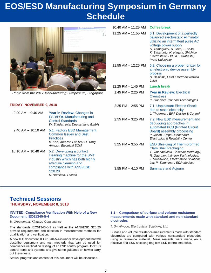
Photo from the 2017 Manufacturing Symposium, Singapore
8
EOS/ESD Manufacturing Symposium in Germany Technical Sessions
1.2 – ESD Risk Analysis using Pulsed AC Ionization Technology
J. Yoo, E. Choi, E. Koo, Core Insight
A decade ago, pulsed AC ionization has introduced to ESD industry as a new ionization technology. Until this time, CPM technology have no problem to measure offset voltage of ionizers. Fast switching voltages could a root cause of sensitive device failures rather than neutralize ESDS items. CPM has lack of measurement for fast swing voltages and some terminology does not well defined in STM3.1 document. ESD event signature measurement has been studied through experiment apparatus set up and real ESDS items in this study.
2.1 – Reducing ESD risks by measuring surface charges at wafer level inside equipment under real process conditions
T. Sebald, P. Molkentin, ESTION Technology GmbH
Standard measuring equipment like hand-held field meters or electrostatic voltmeters are mostly not suitable for measuring electrostatic charges at wafer level under real process conditions due to confined spaces in the tools and the speed at which wafers move through processes. The presentation describes a new test device, which consists of electrostatic field sensors, integrated partly INSIDE a silicon wafer. This device can be handled and used like a normal production wafer while recording the electrostatic charges a production wafer would “see” during normal processing. Real life data from different processes are presented as well as a correlation to electrostatic voltmeter-readings and device readings under different grounding conditions. The use of this device to test in-tool ionizer balance will be introduced.
2.2 – ESD Risk due to Ionization during Reticle Cleaning
F. zur Nieden, S. Seidl, R. Gaertner, Infineon Technologies
Special tools for reticle cleaning are commonly used in front end lithography. Many are equipped with a build-in ionizer in order to neutralize possible charges on the reticle surface. Although good functionality of ionizers can be measured using a charged plate monitor (a charged metal plate is discharged within few seconds), high charging can still be measured with an alternative method with a better resolution over time. Different influences on the charging level such as media, cleaning pressure, materials and method of cleaning are discussed.
INVITED – ESD flooring systems in electronic manufacturing sites
G. Reina, ELBO Service
The usage of ESD floor inside ESD Protected Areas is not mandatory but it is strongly recommended in order to reduce human errors and relative ESD exposures along the production flow. It can be used as a primary meaning of ground for standing people and in conjunction with ESD shoes has to be able to ensure the max HBV “Human Body voltage” level of 100 volt on people that is handling ESD sensitive parts. In addition, it can easily guarantee the equipotential bonding with ESD protection systems that are in contact or could be placed on it by the normal usage; for this reason its attitude to insure a low contact resistance is very important. Users have to consider it a fundamental device, consequently not only ESD performance but many other parameters are relevant including the design of the screed. The study considers mechanical and physical properties, maintenance cost, relationship between resistance and ESD performance.
3.1 – Relationship between footwear resistance and personal grounding through footwear and flooring
J. Smallwood, Electrostatic Solutions, Ltd; D. Swenson, Affinity Static Control Consulting, LLC; T. Viheriaekoski, Cascade Metrology
ESD control footwear is qualified using resistance measurements for use in explosives handling facilities. This paper explores the relationship between footwear resistance and the personal grounding performance in terms of measured resistance from body to ground and body voltage generated in a walk test with “antistatic” and “conductive” floors.
3.2 – ESD Risks of Containers Made of Conductive Compounds
T. Viheriäkoski, Cascade Metrology; E. Kärjä, Premix Oy; P. Horsma-aho Treston Oy; R. Gaertner, Infineon Technologies; J. Smallwood, Electrostatic Solutions, Ltd
ESD risk scenarios of conductive containers were assessed by using a system level test generator and different configurations of discharge electrodes. Energy coupling inside the container can be minimized by an applicable mechanical design. Avoidance of the direct or capacitive drain and return path mitigates energy coupling and reduces ESD risks efficiently.
4.1 – The Risks of Electric Fields for ESD Sensitive Devices
W. Stadler, J. Niemesheim, Intel Deutschland GmbH; S. Seidl, R. Gaertner, Infineon Technologies; T. Viheriaekoski, Cascade Metrology
For objects with different sizes, distances and orientations to an electric field, potentials, charging, and discharge currents of the objects are measured in order to assess the ESD risk due to the E-field. The current rules in ANSI/ESD S20.20 and IEC 61340-5-1 might need an update to cover worst-case scenarios.
4.2 – The revised ESD FORUM e. V. guideline 1013 (2.0) for ESD risk evaluation of robotic process equipment and its countermeasures
P. Jacob Empa Duebendorf, Electronics & Reliability Center
In 2013, a working group of the German ESD FORUM developed a first guideline for ESD risk evaluation of automated process equipment. While it has proved its worth in field practice, numerous feedbacks and proposals were received from users which meanwhile have been implemented. The revised guideline offers additional examples of process equipment evaluations, especially for ESD-critical foil-based processes.
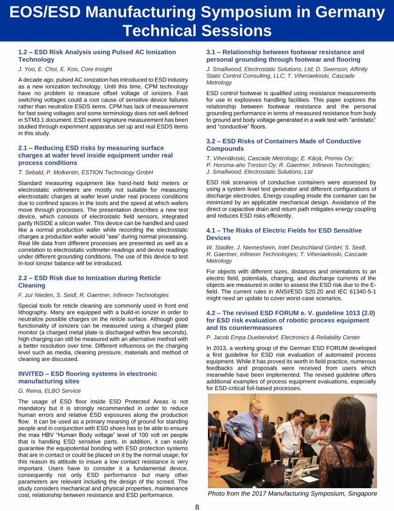
Photo from the 2017 Manufacturing Symposium, Singapore

9
EOS/ESD Manufacturing Symposium in Germany Technical Sessions
FRIDAY, NOVEMBER 9, 2018
YEAR IN REVIEW – Changes in ESD/EOS Manufacturing and Control Standards
W. Stadler, Intel Deutschland GmbH
ESDA and IEC have currently more than 30 active EOS/ESD manufacturing and EOS/ESD control Working Groups. The Working Groups are continuously creating, updating, revising, and reaffirming documents in the field of ESD and EOS control; approximately 40 EOS/ESD control documents are in process every year. The Short Tutorial will give a brief overview of the most important changes of EOS/ESD manufacturing and control standards in the last years and an outlook what can be expected in near future.
5.1 – Factory ESD Management Common Issues and Best Practices
K. Koo, Amazon Lab126; O. Tang, Amazon Electrical SQM
Statistical analysis of audit findings are utilized to address common issues and challenges in ESD management. A systematic ESD management method is introduced here by leveraging product design data, best practices from past project audits, as well as standard ESD control procedures and checklists.
5.2 – Developing a contact cleaning machine for the SMT industry which has both highly effective cleaning and compliance with ANSI/ESD S20.20
S. Hamilton, Teknek
This case study highlights the difficulties of combining two vital functional requirements, cleaning and static control, for the SMT industry and will outline the novel approaches taken to overcome these difficulties.
6.1 – Development of a perfectly balanced electrostatic eliminator utilizing an intermittent pulse AC voltage power supply
S. Yamaguchi, A. Goto, T. Saito, K. Sakamoto, H. Nagata, Shishido Electrostatic, Ltd.; K. Takahashi, Iwate University
A perfectly balanced fan type electrostatic eliminator utilizing an intermittent pulse AC voltage power supply is developed. The short-term fluctuation range of the offset voltage (ion balance) is smaller than ±2 V without a sensor feedback system. The performance is maintained in 2500 h continuous operation.
6.2 – Choosing a proper ionizer for an electronic device assembly process
D. Basiński, Lafot Elektronik Natalia Lalek
The purpose of this paper is to present significant differences in the use of different types of ionizers in the assembly of an electronic device. It is intended to draw attention to certain aspects to consider when choosing a proper ionizer.
YEAR IN REVIEW – Electrical Overstress
R. Gaertner, Infineon Technologies
Electrical overstress (EOS) like damages represent a significant percentage of components returned by the customers to the semiconductor manufacturers for comprehensive failure analysis. Typically expectation is that the failure analysis engineer can determine the root cause for the damage (including damaging waveform) just by looking at the failure picture. But this is generally not possible. Some time ago the Industry Council for ESD target values published a White Paper on EOS with new definitions for EOS based on absolute maximum ratings (AMR) and they introduced a new terminology called EIPD (electrically induced physical damage) to avoid that EOS is used before there is a clear hint to the root cause. They also introduced a fishbone diagram with specific branches for root causes as a guideline for users to perform a fault tree analysis. This work was picked up by the automotive industry where USCAR and the ESDA published a first document on information exchange needed to be able to find the root cause for possible EOS damages (WG27). Based on this new guideline a two level support will be introduced based on an information sharing between the OEM, tier1 and semiconductor manufacturers that can lead to a higher chance to identify the root cause of the damage and allows to focus on the important topics.
7.1 – Unpleasant Electric Shock due to static electricity
J. Thürmer, EPA Design & Control
We all know about ESD damages in the electronic industry, but what about issues in a noodle factory? The presentation is reporting case studies about ESD problems in different parts of the industry like food industry (noodle factory or margarine factory). Even if noodles are not endangered by ESD the static discharge can threaten people handling the products. IEC TR 60079-32 recommends that shocks due to static electricity should always be investigated to exclude a possible risk to personnel by too high charges (50 µC) or too high energy (350 mJ). Other case studies are reporting about problems with plastic injection molding or flooring issues.
7.2 – New ESD measurement and debugging approaches in automated PCB (Printed Circuit Board) assembly processing
P. Jacob Empa Duebendorf, Electronics & Reliability Center
ESD risk evaluation in PCB assembly machines is difficult due to high process speed and virtually impossible in-situ access for measurements. A new measurement approach, based on a test-PCB is presented, allowing the in-situ measurement of imported charging onto the PCB. Surprising results allow challenging conclusions on future ESD control of PCB assembly machines.
7.2 – ESD Shielding of Thermoformed Clam Shell Packaging
Viheriäkoski, Cascade Metrology; R. Gärtner, Infineon Technolo- gies; J. Smallwood, Electrostatic Solutions, Ltd; P. Tamminen, EDR Medeso
Clam shells may provide better ESD protection than shielding bags. Energy coupling in a near field is generally reduced by preventing a direct connection, decreasing capacitive coupling, and increasing breakdown field strength. A properly qualified shielding bag may have unsuspected weakness in ESD protection due to the low breakdown field strength.

10
EOS/ESD Manufacturing Symposium in Germany Exhibits
Promote your company by exhibiting at the 2018 EOS/ESD Manufacturing
Symposium in Germany.
EXHIBITS OPEN: 10:00 AM – 6:00 PM November 8, 2018
9:00 AM – 3:00 PM November 9, 2018
Name of Company: _________________________________________________________________
Street Address: ____________________________________________________________________
City, State, Postal Code: _____________________________________________________________
Country: __________________________________________________________________________
Telephone: ________________________________________________________________________
Contact: _________________________________ Email: ___________________________________
Please provide web address to be used for your link on ESDA website: _________________________
We will exhibit and demonstrate the following products or services: ____________________________
_________________________________________________________________________________
We are Manufacturers Other (please specify): _____________________________________
Amount enclosed $ Check Visa® MasterCard®
American Express® Discover®
Credit card number: ______________________________________ Expiration date: ______________
Name on card: ___________________________________________ Security code: _______________
Cardholder’s signature: ______________________________________________________________
Billing address: _____________________________________________________________________
City: ____________________________ State: _______________ Zip/Postal code: _____________
THE UNDERSIGNED HAS READ AND AGREES TO ABIDE BY THE TERMS ON BOTH SIDES OF THIS APPLICATION.
Application by: __________________________________________ Date: ______________________ (Signature)
NOTES:
1. Each exhibitor receives one (1) symposium registration package for each booth rented.
2. SPACE WILL BE ASSIGNED IN THE ORDER OF RECEIPT OF REGISTRATION
3. Management reserves the right to relocate exhibit space, as necessary, to conform to show regulation
Exhibit Space Rental: $1,000.00 USD FULL PAYMENT DUE WITH REGISTRATION
Requested Booth Space Second choice Third Choice

11
EOS/ESD Manufacturing Symposium in Germany Accommodation
Technical Program Committee (TPC): Rainer Pfeifle, Wolfgang Warmbier GmbH, Hilzingen, Germany (TPC Chair) Frank Biege, Hella KGaA, Lippstadt, Germany Reinhold Gaertner, Infineon Technologies, Munich, Germany Bas Grootemaat, Kingsize Consultancy, Oostrum, The Netherlands Paul Holdstock, Technical Services, Manchester, UK John Kinnear, IBM, Poughkeepsi, NY, USA Giuseppe Reina, EL.BO. Service, S.Lorenzo – Parabiago (MI), Italy Jeremy Smallwood, Electrostatic Solutions, Southampton, UK Wolfgang Stadler, Intel Deutschland GmbH, Neubiberg, Germany Pasi Tamminen, Tampere University of Technology, Tampere, Finland Toni Viheriaekoski, Cascade Metrology, Lohja, Finland
ESD FORUM e.V. Eichendorffstraße 1 D–86720 Noerdlingen Germany Email: [email protected] www.esdforum.de
Management Committee Chairs: Reinhold Gaertner, Infineon Technologies Armin Gottschalk, IQZG Consulting Wolfgang Stadler, Intel Deutschland GmbH
www.esda.org/events/manufacturingsymposium/
NH COLLECTION DRESDEN ALTMARKT Reservations: +1 212 219 7607 Phone: +49 351 501550 Email: [email protected] Address: An der Kreuzkirche 2
D–01067 Dresden Germany

EXHIBITS
12
EOS/ESD Manufacturing Symposium in Germany Registration
REGISTER ONLINE AT www.esda.org
ANSI/ESD S20.20 November 6, 2018 $510 USD
Introduction to Physical Failure Analysis AND
What Information Needs to be Exchanged for
Potential EOS Problem November 6, 2018 $510 USD
Basics of ESD Process Assessment (FC390) November 7, 2018 $510 USD
ESD Basics AND
Packaging of Electrostatic Sensitive Devices AND
ESD and Reliability Estimations November 7, 2018 $510 USD
Symposium only
Technical sessions, Invited talks, and Workshop November 8-9, 2018 $800 USD
Register 5 or more people from one company at the same time for a 10% registration discount per person!
Last Name: _______________________________ First Name: ______________________________
Name of Company: _________________________________________________________________
Street: ___________________________________ City: ____________________________________
State/Province: ________________ Country: __________________ Zip/Postal Code: _____________
Name of Company: _________________________________________________________________
Phone: __________________________________ Email: __________________________________
Setting the Global Standards for Static Control!
EOS/ESD Association, Inc.• 7900 Turin Rd Bld 3 • Rome NY 13440 • http://www.esda.org
Tel: +1-315-339-6937 • Fax: +1-315-339-6793 • Email: [email protected]
Registration Information For credit card payments: Register online at:
EOS/ESD Association http://www.cvent.com/d/pgq5n5 Phone: +1 (315) 339-6937
Other form of payment contact:
EOS/ESD Association 7900 Turin Rd Bld 3 Rome NY 13440 Phone +1 (315) 339 6937 [email protected]