enabling next generation innovation with 22fdx™ update iedm 2015.pdfgrowth in mobile computing ......
TRANSCRIPT

Enabling Next Generation Innovation with 22FDX™ Subramani Kengeri
Vice President, General Management, CMOS Platforms Business Unit
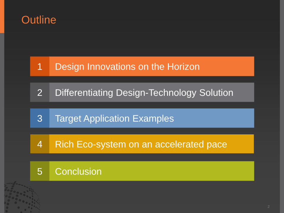
Outline
2
Design Innovations on the Horizon
Differentiating Design-Technology Solution
Target Application Examples
1
2
3
Rich Eco-system on an accelerated pace 4
Conclusion 5
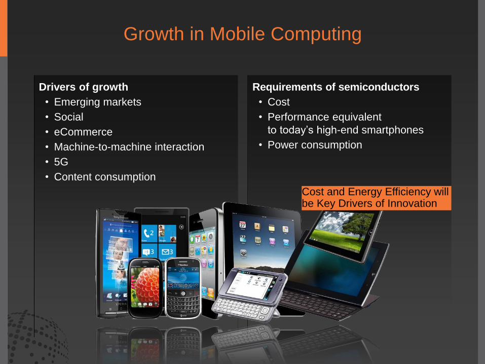
Growth in Mobile Computing
Drivers of growth
• Emerging markets
• Social
• eCommerce
• Machine-to-machine interaction
• 5G
• Content consumption
Requirements of semiconductors
• Cost
• Performance equivalent
to today’s high-end smartphones
• Power consumption
Cost and Energy Efficiency will be Key Drivers of Innovation
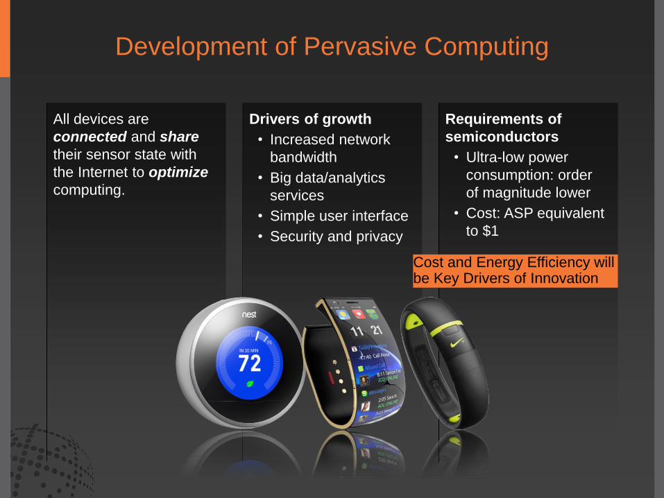
Development of Pervasive Computing
All devices are
connected and share
their sensor state with
the Internet to optimize
computing.
Drivers of growth
• Increased network
bandwidth
• Big data/analytics
services
• Simple user interface
• Security and privacy
Requirements of
semiconductors
• Ultra-low power
consumption: order
of magnitude lower
• Cost: ASP equivalent
to $1
Cost and Energy Efficiency will be Key Drivers of Innovation

Emergence of Intelligent Computing
Elements
• Natural interface
• Real-time
decision-making
• Ambient
• Sensory
• Aware
• Always on
Drivers of growth
• Drones
• Automotive
• Robotics
Requirements of
semiconductors
• Ultra-high
performance:
e.g. 60 fps image
processing
• Very low power
• Cost
Connecting Everything Everywhere
Wireless Network Cloud
Autonomous Cars
Drones / Robots
Smartphones
Wearables
Cost and Energy Efficiency will be Key Drivers of Innovation

COST: The economic foundation on which the semiconductor industry has functioned for 4 decades – is at risk…
6
Wafer cost increase driven by scaling and compounded by - FINFET and double patterning requirements
Historical First: Cost per Transistor is Rising
90nm
65nm
40nm 20nm
16/14nm 28nm
FinFET
Cost Per Million Gates
Technology Node
180nm 130nm 90nm 65nm 40nm 28nm 20nm 14nm
The era in which shrinking features automatically ensured cheaper transistors
is over!
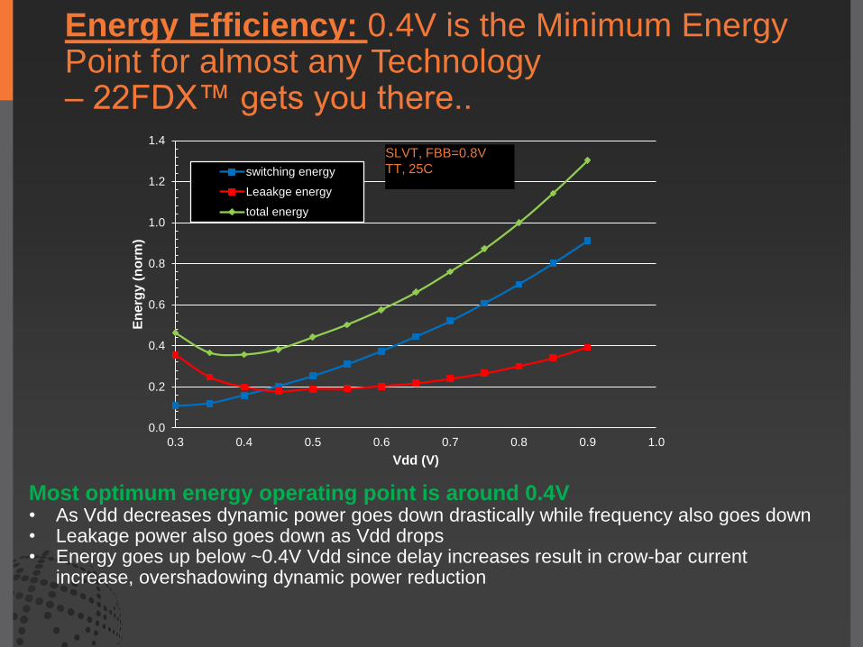
Energy Efficiency: 0.4V is the Minimum Energy Point for almost any Technology – 22FDX™ gets you there..
0.0
0.2
0.4
0.6
0.8
1.0
1.2
1.4
0.3 0.4 0.5 0.6 0.7 0.8 0.9 1.0
En
erg
y (
no
rm)
Vdd (V)
switching energy
Leaakge energy
total energy
SLVT, FBB=0.8V
TT, 25C
Most optimum energy operating point is around 0.4V • As Vdd decreases dynamic power goes down drastically while frequency also goes down • Leakage power also goes down as Vdd drops • Energy goes up below ~0.4V Vdd since delay increases result in crow-bar current
increase, overshadowing dynamic power reduction

FinFET & FD-SOI Solve Different Market Needs
8
Bulk CMOS
Bulk CMOS
Lowest
Cost
FinFET
High
Performance
Ultra-thin Buried
Oxide Insulator
Fully Depleted
Channel for
Low Leakage
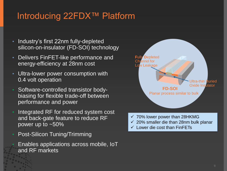
Introducing 22FDX™ Platform
• Industry’s first 22nm fully-depleted silicon-on-insulator (FD-SOI) technology
• Delivers FinFET-like performance and energy-efficiency at 28nm cost
• Ultra-lower power consumption with 0.4 volt operation
• Software-controlled transistor body-biasing for flexible trade-off between performance and power
• Integrated RF for reduced system cost and back-gate feature to reduce RF power up to ~50%
• Post-Silicon Tuning/Trimming
• Enables applications across mobile, IoT and RF markets
9
Ultra-thin Buried Oxide Insulator
Fully Depleted Channel for Low Leakage
FD-SOI Planar process similar to bulk
70% lower power than 28HKMG
20% smaller die than 28nm bulk planar
Lower die cost than FinFETs

Relative Performance
1.0 0.8 0.6 0.4 0.2 1.2
22FDX™ Offers the widest range of Performance/Leakage Optimization points
10
SLVT/LVT • Lowest VT
• Optimized for FBB
• Highest performance
RVT/HVT • Mid-range VT
• Optimized for RBB
• Balance of low leakage
and high performance
Rela
tive L
eakage
0.0
1
10 ULL • Optimized for leakage
• Coupled with RBB achieves
≈1pA/um leakage
100
1000
10000
100000
1000000

22FDX™: Multiple Body-Bias and Vt Points on Same Die
11
Optimize Standby and Dynamic Power
Wireless Comms
High Performance Application Processor
“Watchdog” Processor
Wakes up Image Processor to zoom in and analyze
Detects motion
Wakes up comm block to transmit message
Low static and dynamic power
RF integration for reduced BOM cost
RBB and FBB for power/perf tradeoffs
RBB for lowest leakage
Integrated RF FBB for lowest dynamic power
FD-SOI Delivers:
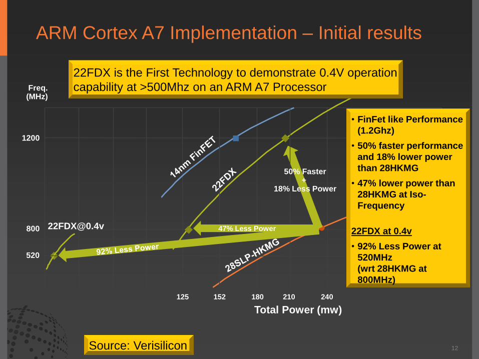
ARM Cortex A7 Implementation – Initial results
12
1200
800
125 240
Total Power (mw)
Freq. (MHz)
180 210 152
520
47% Less Power
• FinFet like Performance
(1.2Ghz)
• 50% faster performance
and 18% lower power
than 28HKMG
• 47% lower power than
28HKMG at Iso-
Frequency
22FDX at 0.4v
• 92% Less Power at
520MHz
(wrt 28HKMG at
800MHz)
22FDX is the First Technology to demonstrate 0.4V operation
capability at >500Mhz on an ARM A7 Processor
Source: Verisilicon
50% Faster +
18% Less Power

22FDX™ Platform Extensions
• 22FDX Base Platform
– 4 Core Vts
– 2 IO Vts @ 1.2/1.5/1.8v
– Passives
– SRAMs (HD, HC, LV, ULV, TP)
– 8T/12T libraries
– Software controlled Forward/Reverse body-bias
13
-ulp adds logic libraries and memory compiler optimized for 0.4v logic operation
-ull adds devices, libraries, and memory compilers to achieve 1pA/um leakage
-uhp adds optimized BEOL stacks, 12T libraries optimized at OD, high-speed SERDES (16/28GHz), and MIM capacitor
-rfa adds RF enablement , BEOL passives, and IP for BTLE, WiFi
Base platform PDK & IP Application-optimized extensions
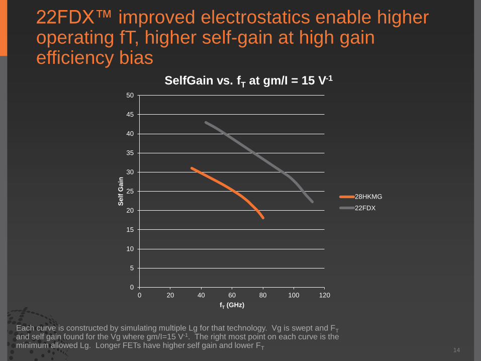
22FDX™ improved electrostatics enable higher operating fT, higher self-gain at high gain efficiency bias
Each curve is constructed by simulating multiple Lg for that technology. Vg is swept and FT and self gain found for the Vg where gm/I=15 V-1. The right most point on each curve is the minimum allowed Lg. Longer FETs have higher self gain and lower FT 14
0
5
10
15
20
25
30
35
40
45
50
0 20 40 60 80 100 120
Self
Gain
fT (GHz)
SelfGain vs. fT at gm/I = 15 V-1
28HKMG
22FDX
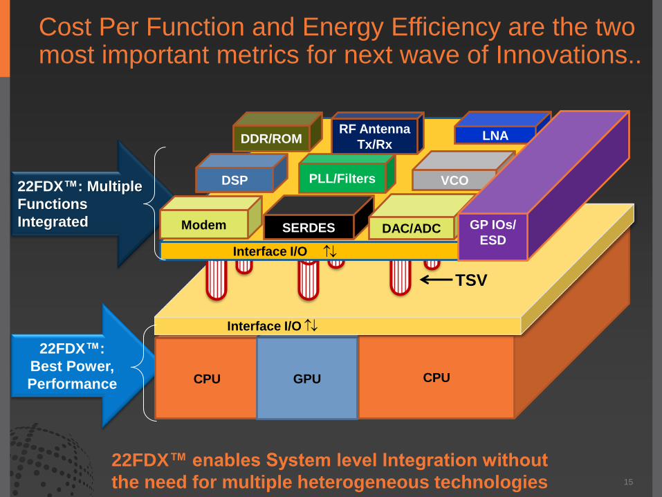
Cost Per Function and Energy Efficiency are the two most important metrics for next wave of Innovations..
15
22FDX™:
Best Power,
Performance CPU GPU CPU
Interface I/O
TSV
22FDX™: Multiple
Functions
Integrated
Interface I/O
DSP
SERDES Modem DAC/ADC
VCO PLL/Filters
RF Antenna
Tx/Rx
LNA DDR/ROM
GP IOs/
ESD
22FDX™ enables System level Integration without
the need for multiple heterogeneous technologies
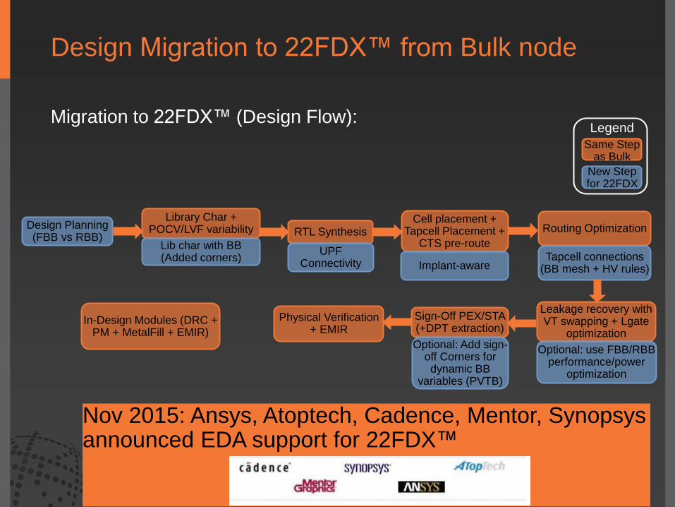
RTL Synthesis Cell placement +
Tapcell Placement + CTS pre-route
Implant-aware
Routing Optimization
Tapcell connections (BB mesh + HV rules)
Leakage recovery with VT swapping + Lgate
optimization
Optional: use FBB/RBB performance/power
optimization
Sign-Off PEX/STA (+DPT extraction)
Optional: Add sign-off Corners for dynamic BB
variables (PVTB)
Physical Verification + EMIR
Library Char + POCV/LVF variability
Lib char with BB (Added corners)
In-Design Modules (DRC + PM + MetalFill + EMIR)
Design Planning (FBB vs RBB)
UPF Connectivity
Design Migration to 22FDX™ from Bulk node
Migration to 22FDX™ (Design Flow):
Same Step as Bulk
New Step for 22FDX
Legend
Nov 2015: Ansys, Atoptech, Cadence, Mentor, Synopsys announced EDA support for 22FDX™

Successful Early Collaboration (TechCon 2015): ARM Cortex-A17 Quad-core Implementation
• Successful Cortex-A17 quad-core implementation using:
– 5 power domains (4 CPU cores + 1 nonCPU module)
– 5 body-bias net pairs (n-well, p-well biasing)
• 1 pair for standard cells
• 2 pairs for L1 cache periphery, bitcell array
• 2 pairs for L2 cache periphery, bitcell array
• Body-bias nets might be shared depending on eventual IP features
• Used our reference flow capability
• Coming Soon:
– Hierarchical low power flow (VDD and BB scaling control)
– In-design added modules (DRC/PM/MetalFill)
– Power and signal EMIR modules
– Integrate BB IP to generate the bias voltages
17
Data Engine
Dside
Iside
Core

22FDX™ Foundation IP – Under Development
18
IP Type IP Description
Foundation IP
Standard Cells High Density, High Performance
Memory Compilers
(a)High Density Single-Port SRAM
(b)High Speed Single-Port SRAM
(c)High Density Single-Port Register File
(d)High Speed Single-Port Register File
(e)High Speed Two-Port Register File
(f) High Density Via ROM
GPIO Voltages TBD and interfaces (SPI, I2C, MMC)
eFuse 4K macro
PLL 2-3 PLLs; Frequency, Jitter, Area, Power TBD
Temperature sensor Support for multiple remote monitors
OTP One-Time Programmable
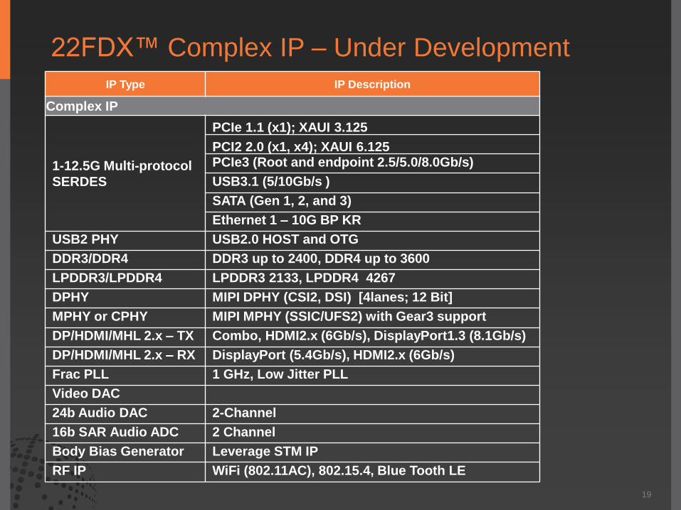
22FDX™ Complex IP – Under Development
19
Complex IP
1-12.5G Multi-protocol
SERDES
PCIe 1.1 (x1); XAUI 3.125
PCI2 2.0 (x1, x4); XAUI 6.125 PCIe3 (Root and endpoint 2.5/5.0/8.0Gb/s)
USB3.1 (5/10Gb/s )
SATA (Gen 1, 2, and 3)
Ethernet 1 – 10G BP KR
USB2 PHY USB2.0 HOST and OTG
DDR3/DDR4 DDR3 up to 2400, DDR4 up to 3600
LPDDR3/LPDDR4 LPDDR3 2133, LPDDR4 4267
DPHY MIPI DPHY (CSI2, DSI) [4lanes; 12 Bit]
MPHY or CPHY MIPI MPHY (SSIC/UFS2) with Gear3 support
DP/HDMI/MHL 2.x – TX Combo, HDMI2.x (6Gb/s), DisplayPort1.3 (8.1Gb/s)
DP/HDMI/MHL 2.x – RX DisplayPort (5.4Gb/s), HDMI2.x (6Gb/s)
Frac PLL 1 GHz, Low Jitter PLL
Video DAC
24b Audio DAC 2-Channel
16b SAR Audio ADC 2 Channel
Body Bias Generator Leverage STM IP
RF IP WiFi (802.11AC), 802.15.4, Blue Tooth LE
IP Type IP Description

FDSOI Has a Bright Future
20
22FDX™ Differentiated features will be extended to 10nm Generation
FDSOI Scaling FinFET Scaling
Strong industry support today – Ecosystem being
established on an accelerated pace Ecosystem established
Scaling roadmap
- Power/Perf demonstrated w/ 14FD
- Boosters defined down to 10FD
Scaling roadmap
- Good electrostatic demonstrated
- Higher effective Device width
Lower Cost / Die
- Fewer mask layers
- Faster learning cycles
Higher Cost & Higher complexity
Back-Gate bias (Software controlled)
- Process / Variability compensation
- Flexible Dynamic vs. Static Power
Back Bias is not Effective
Low-Leakage Devices & Memory
- Reverse body-bias enhances further Higher Leakage in a given foot-print (3D)
Lowest Vmin Device
- Lower intrinsic Capacitance
- Lower intrinsic variability
- Superior Weff tuning for low power
- Forward body-bias
Low Vdd, but inherently higher than FDSOI
- 3D architecture required for electrostatics

22FDX™: The Right Technology at the Right Time
21
High Performance Computing & Switching
Server
IoT, Wearables, Sensors, Low-end Smartphone
High-end Mobile Application Processor
Wired Networking, Consumer Applications Mid-Range Smart phone
28HPP
28SLP
14LPP/
LPE
22FDX
10nm
FD
Next
Node
22FDX™ Design Kits available NOW Next node Target: 10nm FinFET Performance at 20-30% lower die-cost
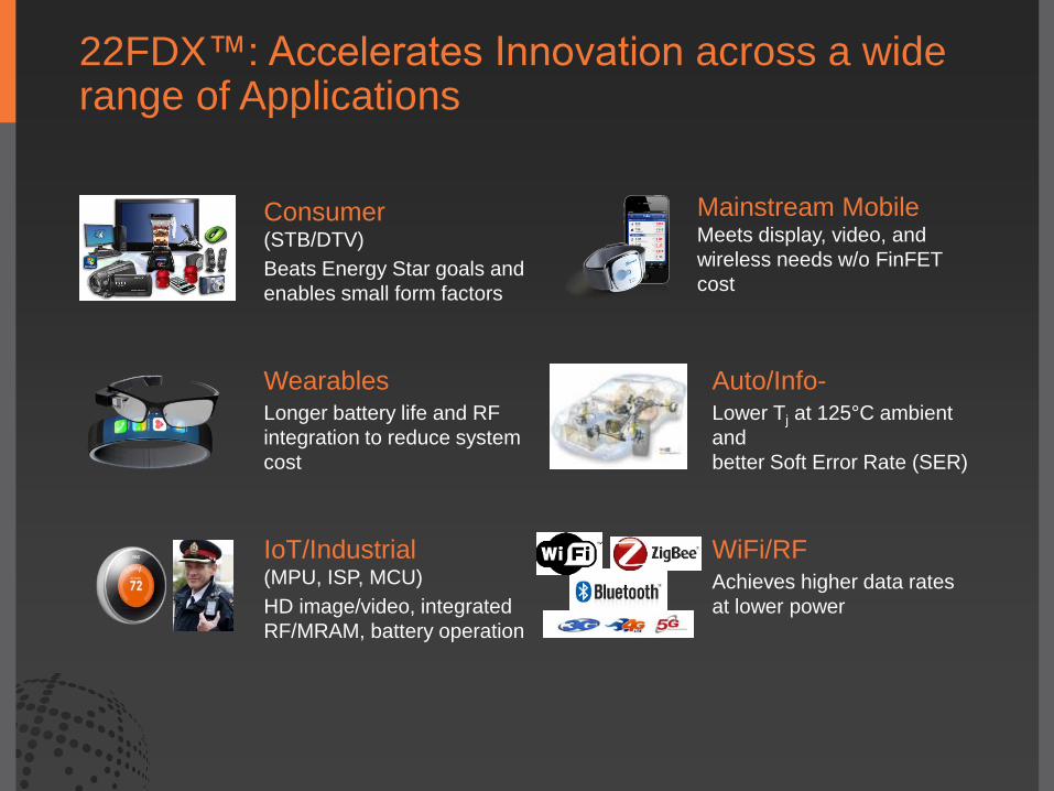
22FDX™: Accelerates Innovation across a wide range of Applications
Consumer (STB/DTV)
Beats Energy Star goals and
enables small form factors
Wearables Longer battery life and RF
integration to reduce system
cost
IoT/Industrial (MPU, ISP, MCU)
HD image/video, integrated
RF/MRAM, battery operation
Mainstream Mobile Meets display, video, and
wireless needs w/o FinFET
cost
Auto/Info- Lower Tj at 125°C ambient
and
better Soft Error Rate (SER)
WiFi/RF Achieves higher data rates
at lower power

Enabling Next Generation Innovation with 22FDX™
22FDX™: The Right Technology at the Right Time
• FinFET-like performance at 28nm cost
• 0.4 Volt Operation offers the best energy efficiency
• Software-controlled transistor body-biasing enables Innovative Power Management schemes
• Integrated eNVM and RF enables lowest cost and smallest form-factor
• Post-Silicon Tuning/Trimming enables differentiation
23
Design Kits available now
Let us Lead the next wave of Innovations together !!

Trademark Attribution
GLOBALFOUNDRIES®, the GLOBALFOUNDRIES logo and combinations thereof, and GLOBALFOUNDRIES’ other trademarks and service marks are owned by GLOBALFOUNDRIES Inc. in the United States and/or other jurisdictions. All other brand names, product names, or trademarks belong to their respective owners and are used herein solely to identify the products and/or services offered by those trademark owners.
© 2015 GLOBALFOUNDRIES Inc. All rights reserved.
Thank you