en6362qi 6a power module datasheet - altera · enpirion® datasheet en6362qi 6a powersoc highly...
TRANSCRIPT

Enpirion® Datasheet EN6362QI 6A PowerSoC
Highly Integrated Synchronous DC-DC Buck with Integrated Inductor
www.altera.com/enpirion
Description
The EN6362QI is a Power System on a Chip (PowerSoC) DC to DC converter with an integrated inductor, PWM controller, MOSFETs and compensation to provide the smallest solution size in an 8x8x3mm 56 pin QFN module. It offers very high efficiency and is able to provide 6A continuous output current with no de-rating. The EN6362QI also provides excellent line and load regulation over temperature. The EN6362QI is specifically designed to meet the precise voltage and fast transient requirements of high-performance, low-power processor, DSP, FPGA, memory boards and system level applications in distributed power architecture.
Other features include precision enable threshold, pre-bias monotonic start-up, and programmable soft-start. The device’s advanced circuit techniques, ultra-high switching frequency, and proprietary integrated inductor technology deliver high-quality, ultra-compact DC-DC conversion.
The Altera Enpirion integrated inductor solution significantly helps to reduce noise. The complete power converter solution enhances productivity by offering greatly simplified board design, layout and manufacturing requirements. All Altera Enpirion products are RoHS compliant and lead-free manufacturing environment compatible.
Features
• High Efficiency (Up to 96%)
• Excellent Ripple and EMI Performance
• Up to 6A Continuous Operating Current
• Input Voltage Range (3.0V to 6.5V)
• 1.5% VFB Accuracy
• Optimized Total Solution Size (160 mm2)
• Precision Enable Threshold for Sequencing
• Programmable Soft-Start
• Pin compatible with the 8A EN6382QI
• Thermal, Over-Current, Short Circuit, ReverseCurrent Limit and Under-Voltage Protections
• RoHS Compliant, MSL Level 3, 260°C Reflow
Applications
• Point of load regulation for FPGAs, ASICs,
processors, DSPs, and distributed power
architectures.
• Industrial automation, servers, storage, adapter
cards, wireless base stations, test and
measurement, and embedded computing.
• Space constrained applications that require the
highest power density.
• Noise sensitive applications.
VOUTVIN
2x22µF1206
VOUT
ENABLE
AGNDSS
PVIN
AVIN
PGND PGND
EN6362QI
15nF
VFB
RA
RB
R1
CA
FQADJ
2x47µF1206
RFQADJ
EN
10Ω
Figure 1: Simplified Applications Circuit Figure 2: Efficiency at VIN = 5V, VOUT = 3.3V
0
20
40
60
80
100
0 1 2 3 4 5 6
Eff
icie
nc
y [
%]
Output Current [A]

EN6362QI
www.altera.com/enpirion Page 2
Ordering Information
Part Number Package Markings Temp Rating (°C) Package Description
EN6362QI EN6362QI -40 to +105 56-pin (8mm x 8mm x 3mm) QFN T&R
EVB-EN6362QI
EN6362QI QFN Evaluation Board
Packing and Marking Information: www.altera.com/support/reliability/packing/rel-packing-and-marking.html
Pin Assignments (Top View)
NC 1
NC
NC
NC
NC
NC
NC
NC
NC
NC
NC
NC
NC
NC
2
3
4
5
6
7
8
9
VO
UT
VO
UT
VO
UT
VO
UT
NC
NC
NC
NC
NC
(SW
)
PG
ND
PG
ND
PVIN
PVIN
PVIN
PVIN
PVIN
PVIN
PVIN
PVINP
GN
D
VDDB
NC
BGND
NC
NC
(SW
)
NC
(SW
)
FQ
AD
J
VS
EN
SE
SS
VFB
AG
ND
AV
IN
ENABLE
PG
OO
D
10
11
12
13
14
15
16
17
18
19
20
21
22
23
24
25
26
27
28
42
41
40
39
38
37
36
35
34
33
32
31
30
29
56
55
54
53
52
51
50
49
48
47
46
45
44
43
PG
ND
NC
(SW
)
NC
(SW
)
NC
NC
NC
NC
57PGND
PG
ND
60NC
59DNC(VIN)
58DNC
(VOUT)
Figure 3: Pin-out Diagram (Top View)
NOTE A: NC pins are not to be electrically connected to each other or to any external signal, ground, or voltage. However, they must be soldered to the PCB. Failure to follow this guideline may result in part malfunction or damage.
NOTE B: White ‘dot’ on top left is pin 1 indicator on top of the device package.
NOTE C: Grayed-out pins are not to be soldered to the PCB. Refer to Figure 9 for the keep-out diagram.
EN6362QI
www.altera.com/enpirion
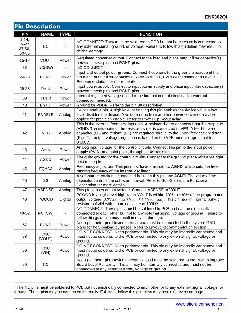
Pin Description
PIN NAME TYPE FUNCTION 1-14, 19-22, 37-38, 53-56
NC - NO CONNECT: They must be soldered to PCB but not be electrically connected to any external signal, ground, or voltage. Failure to follow this guideline may result in device damage.1
15-18 VOUT Power Regulated converter output. Connect to the load and place output filter capacitor(s) between these pins and PGND pins.
23 NC(SW) - NO CONNECT 1
24-28 PGND Power Input and output power ground. Connect these pins to the ground electrode of the input and output filter capacitors. Refer to VOUT, PVIN descriptions and Layout Recommendation for more details.
29-36 PVIN Power Input power supply. Connect to input power supply and place input filter capacitor(s) between these pins and PGND pins.
39 VDDB Power Internal regulated voltage used for the internal control circuitry. No external connection needed.
40 BGND Power Ground for VDDB. Refer to the pin 39 description.
41 ENABLE Analog Device enable pin. A high level or floating this pin enables the device while a low level disables the device. A voltage ramp from another power converter may be applied for precision enable. Refer to Power Up Sequencing.
42 VFB Analog
This is the external feedback input pin. A resistor divider connects from the output to AGND. The mid-point of the resistor divider is connected to VFB. A feed-forward capacitor (CA) and resistor (R1) are required parallel to the upper feedback resistor (RA). The output voltage regulation is based on the VFB node voltage equal to 0.600V.
43 AVIN Power Analog input voltage for the control circuits. Connect this pin to the input power supply (PVIN) at a quiet point, through a 10Ω resistor.
44 AGND Power The quiet ground for the control circuits. Connect to the ground plane with a via right next to the pin.
45 FQADJ Analog Frequency adjust pin. This pin must have a resistor to AGND, which sets the free running frequency of the internal oscillator.
46 SS Analog A soft-start capacitor is connected between this pin and AGND. The value of the capacitor controls the soft-start interval. Refer to Soft-Start in the Functional Description for more details.
47 VSENSE Analog This pin senses output voltage. Connect VSENSE to VOUT.
48 PGOOD Digital PGOOD is a logic level high when VOUT is within -10% to +10% of the programmed output voltage (0.9VOUT_NOM ≤ VOUT ≤ 1.1VOUT_NOM). This pin has an internal pull-up resistor to AVIN with a nominal value of 100kΩ.
49-52 NC (SW) - NO CONNECT: These pins must be soldered to PCB and can be electrically connected to each other but not to any external signal, voltage or ground. Failure to follow this guideline may result in device damage.
57 PGND Power Not a perimeter pin. Device thermal pad must be connected to the system GND plane for heat-sinking purposes. Refer to Layout Recommendation section.
58 DNC
(VOUT) Power
DO NOT CONNECT: Not a perimeter pin. This pin may be internally connected and must not be soldered to the PCB or connected to any external signal, voltage or ground.
59 DNC (VIN)
Power DO NOT CONNECT: Not a perimeter pin. This pin may be internally connected and must not be soldered to the PCB or connected to any external signal, voltage or ground.
60 NC - Not a perimeter pin. Device mechanical pad must be soldered to the PCB to improve Board Level Reliability. This pin may be internally connected and must not be connected to any external signal, voltage or ground. 1
1 The NC pins must be soldered to PCB but not electrically connected to each other or to any external signal, voltage, or ground. These pins may be connected internally. Failure to follow this guideline may result in device damage.

EN6362QI
www.altera.com/enpirion Page 4
Absolute Maximum Ratings
CAUTION: Absolute Maximum ratings are stress ratings only. Functional operation beyond the recommended operating conditions is not implied. Stress beyond the absolute maximum ratings may impair device life. Exposure to absolute maximum rated conditions for extended periods may affect device reliability.
PARAMETER SYMBOL MIN MAX UNITS
PVIN, AVIN, VOUT vs. AGND, BGND and PGND shorted -0.3 7.0 V
EN, PGOOD vs. AGND, BGND and PGND shorted -0.3 VIN+0.3 V
VFB, SS, FQADJ vs. AGND, BGND and PGND shorted -0.3 2.5 V
Storage Temperature Range TSTG -65 150 °C
Maximum Operating Junction Temperature TJ-ABS Max 150 °C
Reflow Temp, 10 Sec, MSL3 JEDEC J-STD-020A 260 °C
ESD Rating (based on Human Body Model) 2000 V
ESD Rating (based on CDM) 500 V
Recommended Operating Conditions
PARAMETER SYMBOL MIN MAX UNITS
Input Voltage Range VIN 3.0 6.5 V
Output Voltage Range VOUT 0.60 VIN – VDO 2 V
Operating Junction Temperature TJ -40 +125 °C
Thermal Characteristics
PARAMETER SYMBOL TYP UNITS
Thermal Resistance: Junction to Ambient (0 LFM) 3 JA 16 °C/W
Thermal Resistance: Junction to Case (0 LFM) JC 1 °C/W
Thermal Shutdown TSD 150 °C
Thermal Shutdown Hysteresis TSDH 25 °C
2 VDO (dropout voltage) is defined as (ILOAD x Dropout Resistance). Please refer to Electrical Characteristics Table. 3 Based on 2oz. external copper layers and proper thermal design in line with EIJ/JEDEC JESD51-7 standard for high thermal conductivity boards.
EN6362QI
www.altera.com/enpirion Page 5
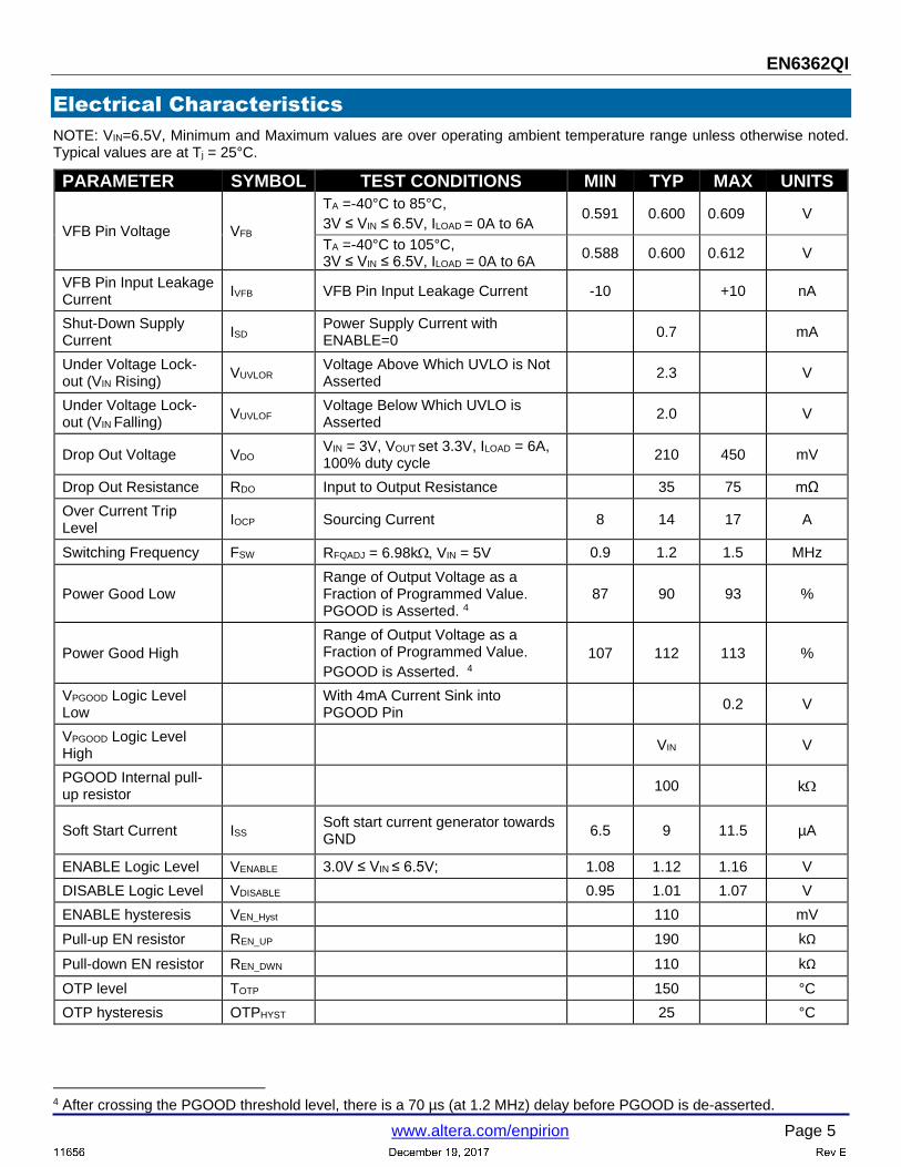
Electrical Characteristics
NOTE: VIN=6.5V, Minimum and Maximum values are over operating ambient temperature range unless otherwise noted. Typical values are at Tj = 25°C.
PARAMETER SYMBOL TEST CONDITIONS MIN TYP MAX UNITS
VFB Pin Voltage VFB
TA =-40°C to 85°C,
3V ≤ VIN ≤ 6.5V, ILOAD = 0A to 6A 0.591 0.600 0.609 V
TA =-40°C to 105°C, 3V ≤ VIN ≤ 6.5V, ILOAD = 0A to 6A
0.588 0.600 0.612 V
VFB Pin Input Leakage Current
IVFB VFB Pin Input Leakage Current -10 +10 nA
Shut-Down Supply Current
ISD Power Supply Current with ENABLE=0
0.7 mA
Under Voltage Lock-out (VIN Rising)
VUVLOR Voltage Above Which UVLO is Not Asserted
2.3 V
Under Voltage Lock-out (VIN Falling)
VUVLOF Voltage Below Which UVLO is Asserted
2.0 V
Drop Out Voltage VDO VIN = 3V, VOUT set 3.3V, ILOAD = 6A, 100% duty cycle
210 450 mV
Drop Out Resistance RDO Input to Output Resistance 35 75 mΩ
Over Current Trip Level
IOCP Sourcing Current 8 14 17 A
Switching Frequency FSW RFQADJ = 6.98kVIN = 5V 0.9 1.2 1.5 MHz
Power Good Low Range of Output Voltage as a Fraction of Programmed Value. PGOOD is Asserted. 4
87 90 93 %
Power Good High
Range of Output Voltage as a Fraction of Programmed Value.
PGOOD is Asserted. 4
107 112 113 %
VPGOOD Logic Level Low
With 4mA Current Sink into PGOOD Pin
0.2 V
VPGOOD Logic Level High
VIN V
PGOOD Internal pull-up resistor
100 k
Soft Start Current ISS Soft start current generator towards GND
6.5 9 11.5 µA
ENABLE Logic Level VENABLE 3.0V ≤ VIN ≤ 6.5V; 1.08 1.12 1.16 V
DISABLE Logic Level VDISABLE 0.95 1.01 1.07 V
ENABLE hysteresis VEN_Hyst 110 mV
Pull-up EN resistor REN_UP 190 kΩ
Pull-down EN resistor REN_DWN 110 kΩ
OTP level TOTP 150 °C
OTP hysteresis OTPHYST 25 °C
4 After crossing the PGOOD threshold level, there is a 70 µs (at 1.2 MHz) delay before PGOOD is de-asserted.

EN6362QI
www.altera.com/enpirion Page 6
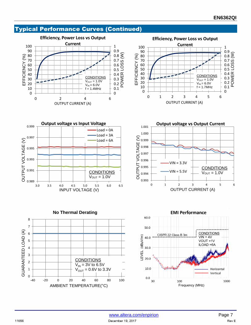
Typical Performance Curves
0
20
40
60
80
100
0 1 2 3 4 5 6
EF
FIC
IEN
CY
(%
)
OUTPUT CURRENT (A)
Efficiency vs Output Current
VOUT = 1V
VOUT = 1.2V
VOUT = 1.8V
0
20
40
60
80
100
0 1 2 3 4 5 6
EF
FIC
IEN
CY
(%
)
OUTPUT CURRENT (A)
Efficiency vs Output Current
VOUT = 1VVOUT = 1.2VVOUT = 1.8VVOUT = 2.5VVOUT = 3.3V
0
10
20
30
40
50
60
70
80
90
100
0 1 2 3 4 5 6
EF
FIC
IEN
CY
(%
)
OUTPUT CURRENT (A)
Efficiency vs Output Current
VIN = 3.3V
VIN = 5V
VIN = 5.5V
0.5
1
1.5
4 9 14 19
FR
EQ
UE
NC
Y (
MH
z)
RFQADJ (kΩ)
Frequency vs RFQADJ
00.10.20.30.40.50.60.70.80.91
0102030405060708090
100
0 1 2 3 4 5 6
PO
WE
R L
OS
S (
W)
EF
FIC
IEN
CY
(%
)
OUTPUT CURRENT (A)
Efficiency, Power Loss vs Output Current
00.10.20.30.40.50.60.70.80.91
0102030405060708090
100
0 1 2 3 4 5 6
PO
WE
R L
OS
S (
W)
EF
FIC
IEN
CY
(%
)
OUTPUT CURRENT (A)
Efficiency, Power Loss vs Output Current
CONDITIONS VIN = 3.3V
CONDITIONS VIN = 5.0V
CONDITIONS VOUT = 1.0V
CONDITIONS VOUT = 1.0V VIN = 6.0V f = 0.7MHz
CONDITIONS VOUT = 1.0V VIN = 6.0V f = 1MHz
EN6362QI
www.altera.com/enpirion Page 7
Typical Performance Curves (Continued)
00.10.20.30.40.50.60.70.80.91
0102030405060708090
100
0 2 4 6
PO
WE
R L
OS
S (
W)
EF
FIC
IEN
CY
(%
)
OUTPUT CURRENT (A)
Efficiency, Power Loss vs Output Current
00.10.20.30.40.50.60.70.80.91
0102030405060708090
100
0 1 2 3 4 5 6
PO
WE
R L
OS
S (
W)
EF
FIC
IEN
CY
(%
)
OUTPUT CURRENT (A)
Efficiency, Power Loss vs Output Current
0.989
0.991
0.993
0.995
0.997
0.999
3.0 3.5 4.0 4.5 5.0 5.5 6.0 6.5
OU
TP
UT
VO
LT
AG
E (
V)
INPUT VOLTAGE (V)
Output voltage vs Input Voltage
Load = 0A
Load = 3A
Load = 6A
0.993
0.994
0.995
0.996
0.997
0.998
0.999
1.000
1.001
0 1 2 3 4 5 6
OU
TP
UT
VO
LT
AG
E (
V)
OUTPUT CURRENT (A)
Output voltage vs Output Current
VIN = 3.3V
VIN = 5.5V
0
1
2
3
4
5
6
7
8
-40 -20 0 20 40 60 80 100
GU
AR
AN
TE
ED
LO
AD
(A
)
AMBIENT TEMPERATURE(°C)
No Thermal Derating
CONDITIONSVIN = 3V to 6.5VVOUT = 0.6V to 3.3V
CONDITIONS VOUT = 1.0V VIN = 6.0V f = 1.4MHz
CONDITIONS VOUT = 1.0V VIN = 6.0V f = 1.7MHz
CONDITIONS VOUT = 1.0V
CONDITIONS VOUT = 1.0V

EN6362QI
www.altera.com/enpirion Page 8
Typical Performance Characteristics

EN6362QI
www.altera.com/enpirion Page 10
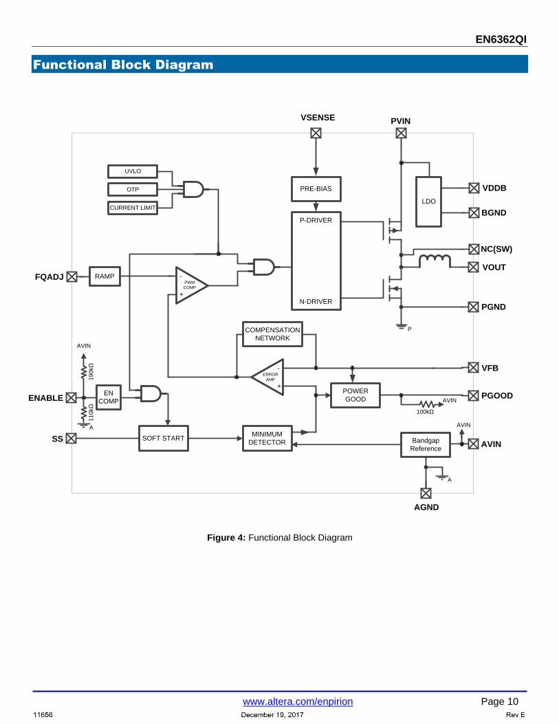
Functional Block Diagram
SOFT START
POWER
GOOD
Bandgap
Reference
COMPENSATION
NETWORK
OTP
UVLO
CURRENT LIMIT
P-DRIVER
N-DRIVER
RAMP
AVIN
MINIMUM
DETECTOR
AVIN
LDO
100kΩ
19
0kΩ
-
+
PWM
COMP
-
+
ERROR
AMP
FQADJ
ENABLE
SS
PVIN
AVIN
VDDB
BGND
NC(SW)
VOUT
PGND
VFB
PGOOD
AVIN
VSENSE
AGND
EN
COMP
11
0kΩ
A
A
P
PRE-BIAS
Figure 4: Functional Block Diagram

EN6362QI
www.altera.com/enpirion Page 11
Functional Description
The EN6362QI is a synchronous buck power supply with integrated power MOSFET switches and integrated inductor. The switching supply uses voltage mode control and a low noise PWM topology. The nominal input voltage range is 3.0 - 6.5 volts. The output voltage is programmed using an external resistor divider network. The feedback control loop incorporates a type IV voltage mode control design. Type IV voltage mode control maximizes control loop bandwidth and maintains excellent phase margin to improve transient performance. Although the EN6362QI is guaranteed to support up to 6A continuous output current operation over the full ambient temperature range (thermal design), the peak current supported before reaching OCP is substantially higher, exceeding 10A. The operating switching frequency can be adjusted by an external resistor between 0.7MHz and 1.7MHz. The high switching frequency enables the use of small-size input and output capacitors.
EN6362QI electrical features at a glance:
• Precision Enable Threshold
• Soft-Start
• Pre-bias Start-Up
• Resistor Programmable Switching Frequency
• Power Good
• Over-Current/Short Circuit Protection
• Reverse Current Limit (RCL)
• Thermal Shutdown (OTP) with Hysteresis
• Under-Voltage Lockout
Precision Enable
The ENABLE threshold is a precision analog voltage rather than a digital logic threshold. A precision voltage reference and a comparator circuit are kept powered up even when ENABLE is de-asserted. The narrow voltage gap between ENABLE Logic Low and ENABLE Logic High (about 100mV hysteresis) allows the device to turn on at a precise enable voltage level. The precise enable threshold, in conjunction with the proper choice of soft-start capacitors allows accurate sequencing for multiple power supplies. ENABLE has a 2ms lockout time that prevents the device from re-enabling immediately after it has been disabled.
Soft-Start
The SS pin, in conjunction with a small external capacitor between this pin and AGND provides the soft-start function, designed to limit in-rush current during start-up. When the part is enabled, soft-start (SS) current generator charges the SS capacitor in a linear manner. As long as the SS voltage level is smaller than the feedback reference (about 0.6V) the SS voltage is used as feedback reference, ensuring a linear increase of the output voltage. Once the voltage on the SS capacitor reaches 0.6V, the minimum detector (Figure 4) will select the bandgap reference as target, while the voltage across the SS capacitor will continue ramping up until it reaches about 1.5V. As the SS voltage slew rate depends on the SS capacitor, so does the output voltage.
The rise time is defined as the time needed by the output voltage to go from zero to 95% of the programmed value. The rise time (tRISE) is given by the following equation:
tRISE [ms] = Css [nF] x 0.065
There are no limitations regarding the value of the SS capacitor, but the usual range is between 10nF and 100nF.
Pre-Bias Start-up
The EN6362QI supports startup into a pre-biased load. A proprietary circuit ensures the output voltage rises up from the pre-bias value to the programmed output voltage. Start-up is guaranteed to be monotonic for pre-bias voltages in the range of 20% to 75% of the programmed output voltage with a minimum pre-bias voltage of 300mV. Outside of the 20% to 75% range, the output voltage rise will not be monotonic. For this feature to work properly, the EN6362 must be enabled after VIN ramped up.
EN6362QI
www.altera.com/enpirion Page 12
Resistor Programmable Frequency
The operation of the EN6362QI can be optimized by a proper choice of the RFQADJ resistor.
If high efficiency is the most important factor, then a lower switching frequency should be selected. If a better transient response is the most important factor, a higher switching frequency should be selected.
The typical Frequency vs RFQADJ relationship over the suggested range of RFQADJ is shown in the typical performance curves.
PGOOD Operation
The PGOOD pin is used only to signal whether the output voltage is within the specified range. The PGOOD signal is asserted high when the rising output voltage exceeds 92% of the programmed output voltage.
If the output voltage falls outside the range (roughly 90% to 110%), PGOOD remains asserted for the de-glitch time (about 70µs at 1.2MHz switching frequency). After the de-glitch time, PGOOD is de-asserted. PGOOD is also de-asserted if the output voltage exceeds 110% of the programmed output voltage.
Over Current Protection
The current level is sensed through the High Side Switch. The OCP trip point is nominally set around 14A. When the sensed current exceeds the current limit level, both power FETs are turned off for the rest
of the switching cycle. If for the next cycle the over-current condition is removed, the PWM operation will resume. In the event the OCP circuit trips at least 8 consecutive PWM cycles, the device enters a hiccup mode; the device is disabled for about 27ms and restarted with a normal soft-start. This cycle can continue indefinitely as long as the over current condition persists.
Over Temperature Protection
Temperature sensing circuits in the controller will disable operation when the junction temperature exceeds approximately 150ºC. Once the junction temperature drops by approximatively 25ºC, the converter will resume operation with a normal soft-start.
Input Under-Voltage Lock-Out
When the rising input voltage is below the required voltage level (VUVLOR), switching is inhibited; the lock-out threshold has hysteresis to prevent chatter, thus when the device is operating around the UVLO limit, the input voltage has to fall below the lower threshold (VUVLOF) for the device to stop switching.
Reverse Current Limit protection In order to prevent excessive current buildup in the low side MOSFET, a Reverse Current Limit protection is used; if the Low side MOSFET is kept on during two full PWM cycles, the output will be left floating for the next three cycles. This is an effective method of protecting the low side MOSFET against Over-Current during boost-back.
EN6362QI
www.altera.com/enpirion Page 13
Application Information
Output Voltage Programming and loop Compensation
The EN6362QI output voltage is programmed using a simple resistor divider network. A phase lead capacitor plus a resistor are required for stabilizing the loop. Figure 5 shows the required components and the equations to calculate their values.
The EN6362QI output voltage is determined by resistor divider between VOUT and AGND with the midpoint going to VFB. During steady state operation, the voltage presented at the VFB pin is equal to the internal voltage reference.
Most of EN6362QI compensation network is integrated; however, a phase lead capacitor and a resistor are required in parallel with the upper resistor of the external feedback network.
Total compensation is optimized for use with two 47μF output capacitors and will result in a wide loop bandwidth and excellent load transient performance for most applications. Additional capacitance may be placed beyond the voltage sensing point outside the control loop. Voltage mode operation provides high noise immunity at light load.
In some cases, modifications to the compensation or output capacitance may be required to optimize device performance such as transient response, ripple, or hold-up time. The EN6362QI provides the capability to modify the control loop response to allow for customization for such applications. A simulation model is available upon request.
VOUT
RA
A
RB
CA
RC
VFB
Figure 5: External Feedback/Compensation Network
The feedback and compensation network values depend on the input voltage and output voltage. The external feedback and compensation network values can be calculated using the equations below.
𝑅𝐴 = 294𝑘𝛺
RA value must be rounded up to closest standard value
𝑅𝐵 =𝑉𝐹𝐵×𝑅𝐴
𝑉𝑂𝑈𝑇 − 𝑉𝐹𝐵
where VFB = 0.6V.
RB value must be rounded to closest standard value
Table 1: Recommended Compensation Values
VIN (V) Vout (V) RA (kΩ) CA (pF) RC (kΩ)
All VIN ≥ 1.8 294 10 15
≥4.5 <1.8 294 10 15
<4.5 <1.8 294 22 20.5
Table 1 shows the recommended values for the compensation components.
The output voltage should be sensed close to the most distant capacitor from the local output decoupling. All components from the compensation network must be placed as close as possible to the EN6362, and the output-voltage-feedback, low-impedance trace should go directly to the controller, keeping the high impedance VFB trace as short as possible.
In order to keep the feedback signal as clean as possible, it is recommended to connect RB directly to the AGND pin, rather than going through the GND plane.
Input Capacitor Selection
The EN6362QI has been optimized for use with two 1206 22µF input capacitors. Low ESR ceramic capacitors are required with X5R or X7R dielectric formulation. Y5V or equivalent dielectric formulations must not be used, as these significantly lose capacitance over frequency, temperature and bias voltage.
In some applications, lower value ceramic capacitors may be needed in parallel with the larger capacitors in order to provide high frequency decoupling. The capacitors shown in the
Table 2 are typical input capacitors. Other capacitors with similar characteristics may also be used.

EN6362QI
www.altera.com/enpirion Page 14
Table 2: Recommended Input Capacitors
Description MFG P/N 22µF, 10V, 20%
X5R, 1206 (2 capacitors needed)
Murata GRM31CR61A226ME19L
Taiyo Yuden LMK316BJ226ML-T
Output Capacitor Selection
The EN6362QI has been optimized for use with two 1206 47µF output capacitors. Low ESR, X5R or X7R ceramic capacitors are recommended as the primary choice. Y5V or equivalent dielectric formulations must not be used as these significantly lose capacitance over frequency, temperature and bias voltage. The capacitors shown in the Table 3 are typical output capacitors. Other capacitors with similar characteristics may also be used. Additional bulk capacitance from 100µF to 1000µF may be placed beyond the voltage sensing point outside the control loop. This additional capacitance should have a minimum 6mΩ ESR to ensure stable operation. Most tantalum capacitors will have more than 6mΩ of ESR and may be used without special care. Adding distance in layout may help increase the ESR between the feedback sense point and the bulk capacitors.
Table 3: Recommended Output Capacitors
Description MFG P/N 47µF, 10V, 20%
X5R, 1206 (2 capacitors needed)
Taiyo Yuden LMK316BJ476ML-T
47µF, 6.3V, 20% X5R, 1206
(2 capacitors needed)
Murata GRM31CR60J476ME19L
Taiyo Yuden JMK316BJ476ML-T
10µF, 6.3V, 10% X7R, 0805
(Optional 1 capacitor in parallel with 2x47µF)
Murata GRM21BR70J106KE76L
Taiyo Yuden JMK212B7106KG-T
Output ripple voltage is primarily determined by the aggregate output capacitor impedance. Placing multiple capacitors in parallel reduces the impedance and hence will result in lower ripple voltage.
nTotal ZZZZ
1...
111
21
Table 4: Typical Ripple Voltages
Output Capacitor Configuration
Typical Output Ripple (mVp-p)
2 x 47 µF <10mV † 20 MHz bandwidth limit measured on Evaluation Board
EN6362QI
www.altera.com/enpirion Page 15
Thermal Considerations
Thermal considerations are important power supply design facts that cannot be avoided in the real world. Whenever there are power losses in a system, the heat that is generated by the power dissipation needs to be accounted for. The Altera Enpirion PowerSoC helps alleviate some of those concerns.
The Altera Enpirion EN6362QI DC-DC converter is packaged in an 8x8x3mm 56-pin QFN package. The QFN package is constructed with copper lead frames that have exposed thermal pads. The exposed thermal pad on the package should be soldered directly on to a copper ground pad on the printed circuit board (PCB) to act as a heat sink. The maximum recommended junction temperature for continuous operation is 125°C. Continuous operation above 125°C may reduce long-term reliability. The device has a thermal overload protection circuit designed to turn off the device at an approximate junction temperature value of 150°C.
The EN6362QI is guaranteed to support the full 6A output current up to 105°C ambient temperature. The following example and calculations illustrate the thermal performance of the EN6362QI.
Example:
VIN = 5.5V
VOUT = 1.0V
IOUT = 6A
First calculate the output power.
POUT = 1.0V x 6A = 6.0W
Next, determine the input power based on the efficiency (η) shown in Figure 6.
Figure 6: Efficiency VIN =5.5V, VOUT = 1.0V
For VIN = 5.5V, VOUT = 1.0V at 6A, η ≈ 88%
η = POUT / PIN = 88% = 0.88
PIN = POUT / η
PIN ≈ 6.0W / 0.88 ≈ 6.818W
The power dissipation (PD) is the power loss in the system and can be calculated by subtracting the output power from the input power.
PD = PIN – POUT
≈ 6.818W – 6.0W ≈ 0.818W
With the power dissipation known, the temperature rise in the device may be estimated based on the theta JA value (θJA). The θJA parameter estimates how much the temperature will rise in the device for every watt of power dissipation. The EN6362QI has a θJA value of 16 ºC/W without airflow.
Determine the change in temperature (ΔT) based on PD and θJA.
ΔT = PD x θJA
ΔT ≈ 0.818W x 16°C/W = 13.088°C ≈ 13.1°C
The junction temperature (TJ) of the device is approximately the ambient temperature (TA) plus the change in temperature. We assume the initial ambient temperature to be 25°C.
TJ = TA + ΔT
TJ ≈ 25°C + 13.1°C ≈ 38.1°C
With 0.818W dissipated into the device, the TJ will be 38.1°C.
The maximum operating junction temperature (TJMAX) of the device is 125°C, so the device can operate at a higher ambient temperature. The maximum ambient temperature (TAMAX) allowed can be calculated.
TAMAX = TJMAX – PD x θJA
≈ 125°C – 13.1°C ≈ 111.9°C
The ambient temperature can actually rise by another 86.9°C, bringing it to 111.9°C before the device will reach TJMAX. This indicates that the EN6362QI can support the full 6A output current range up to approximately 112°C ambient temperature given the input and output voltage conditions. This allows the EN6362QI to guarantee full 6A output current capability at 105°C with room for margin. Note that the efficiency will be slightly lower at higher temperatures and this estimate will be slightly lower.
0
10
20
30
40
50
60
70
80
90
100
0 1 2 3 4 5 6
Eff
icie
nc
y [
%]
Output Current [A]
EN6362QI
www.altera.com/enpirion Page 16
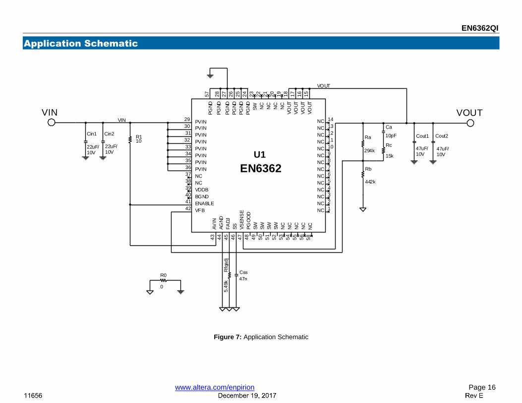
Application Schematic
U1
EN6362
NC 1NC 2NC 3NC 4NC 5NC 6NC 7NC 8NC 9NC 10NC 11NC 12NC 13NC 14
VO
UT
15
VO
UT
16
VO
UT
17
VO
UT
18
NC
19
NC
20
NC
21
NC
22
SW
23
PG
ND
24
PG
ND
25
PG
ND
26
PG
ND
27
PG
ND
28
VFB42ENABLE41BGND40VDDB39NC38NC37PVIN36PVIN35PVIN34PVIN33PVIN32PVIN31PVIN30PVIN
29
PG
OO
D4
8V
SE
NS
E4
7S
S4
6F
AD
J4
5A
GN
D4
4A
VIN
43
PG
ND
57
SW
49
SW
50
SW
51
SW
52
NC
53
NC
54
NC
55
NC
56
`
Cin1
22uF/10V
R0
0
Cin2
22uF/10V
Ra
294k
Cout2
47uF/10V
Rfq
ad
j5.4
9k
Rc
15k
Rb
442k
R110
Ca
10pF Cout1
47uF/10V
VOUT
VOUT
VINVIN
NC
58
Figure 7: Application Schematic

EN6362QI
www.altera.com/enpirion Page 17
Layout Recommendation
Figure 8. Top Layout with Critical Components Only (Top View). See Figure 7 for corresponding
schematic.
This layout only shows the critical components and top layer traces for minimum footprint in single-supply mode with ENABLE tied to AVIN.
Recommendation 1: Input and output filter capacitors should be placed on the same side of the PCB, and as close to the EN6362QI package as possible. They should be connected to the device with very short and wide traces. Do not use thermal reliefs or spokes when connecting the capacitor pads to the respective nodes. The +V and GND traces between the capacitors and the EN6362QI should be as close to each other as possible so that the gap between the two nodes is minimized, even under the capacitors.
Recommendation 2: The PGND connections for the input and output capacitors on layer 1 need to have a slit between them in order to provide some separation between input and output current loops.
Recommendation 3: The system ground plane should be on the 2nd layer (below the surface layer).
This ground plane should be continuous and un-interrupted.
Recommendation 4: The thermal pad underneath the component must be connected to the system ground plane through as many VIAs as possible. The drill diameter of the VIAs should be 0.33mm, and the VIAs must have at least 1 oz. copper plating on the inside wall, making the finished hole size around 0.20-0.26mm. Do not use thermal reliefs or spokes to connect the VIAs to the ground plane. This connection provides the path for heat dissipation from the converter.
Recommendation 5: Multiple small VIAs (the same size as the thermal VIAs discussed in recommendation 4) should be used to connect ground terminal of the input capacitor and output capacitors to the system ground plane. It is preferred to put these VIAs along the edge of the GND copper closest to the +V copper. These VIAs connect the input/output filter capacitors to the GND plane, and help reduce parasitic inductances in the input and output current loops.
Recommendation 6: AVIN is the power supply for the internal small-signal control circuits. It should be connected to the input voltage at a quiet point. In Figure 8 this connection is made at the input capacitor furthest from the PVIN pin and on the input source side. Avoid connecting AVIN near the PVIN pin even though it is the same node as the input ripple is higher there.
Recommendation 7: The VOUT sense point should be connected at the last output filter capacitor furthest from the VOUT pins. Keep the sense trace as short as possible in order to avoid noise coupling into the control loop.
Recommendation 8: Keep RA, CA, RC and RB close to the VFB pin (see Figure 8). The VFB pin is a high-impedance, sensitive node. Keep the trace to this pin as short as possible. Whenever possible, connect RB directly to the AGND pin instead of going through the GND plane. The AGND should connect to the PGND at a single point from the AGND pin to the PGND plane on the 2nd layer.
Recommendation 9: The layer 1 metal under the device must not be more than shown in Figure 9. See the following section regarding Exposed Metal on Bottom of Package. As with any switch-mode DC-DC converter, try not to run sensitive signal or control lines underneath the converter package on other layers.
EN6362QI
www.altera.com/enpirion Page 18
Design Considerations for Lead-Frame Based Modules
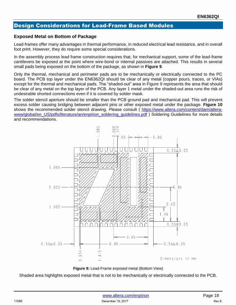
Exposed Metal on Bottom of Package
Lead-frames offer many advantages in thermal performance, in reduced electrical lead resistance, and in overall foot print. However, they do require some special considerations.
In the assembly process lead frame construction requires that, for mechanical support, some of the lead-frame cantilevers be exposed at the point where wire-bond or internal passives are attached. This results in several small pads being exposed on the bottom of the package, as shown in Figure 9.
Only the thermal, mechanical and perimeter pads are to be mechanically or electrically connected to the PC board. The PCB top layer under the EN6362QI should be clear of any metal (copper pours, traces, or VIAs) except for the thermal and mechanical pads. The “shaded-out” area in Figure 9 represents the area that should be clear of any metal on the top layer of the PCB. Any layer 1 metal under the shaded-out area runs the risk of undesirable shorted connections even if it is covered by solder mask.
The solder stencil aperture should be smaller than the PCB ground pad and mechanical pad. This will prevent excess solder causing bridging between adjacent pins or other exposed metal under the package. Figure 10 shows the recommended solder stencil drawing. Please consult ( https://www.altera.com/content/dam/altera-www/global/en_US/pdfs/literature/an/enpirion_soldering_guidelines.pdf ) Soldering Guidelines for more details and recommendations.
Figure 9: Lead-Frame exposed metal (Bottom View)
Shaded area highlights exposed metal that is not to be mechanically or electrically connected to the PCB.
EN6362QI
www.altera.com/enpirion Page 19
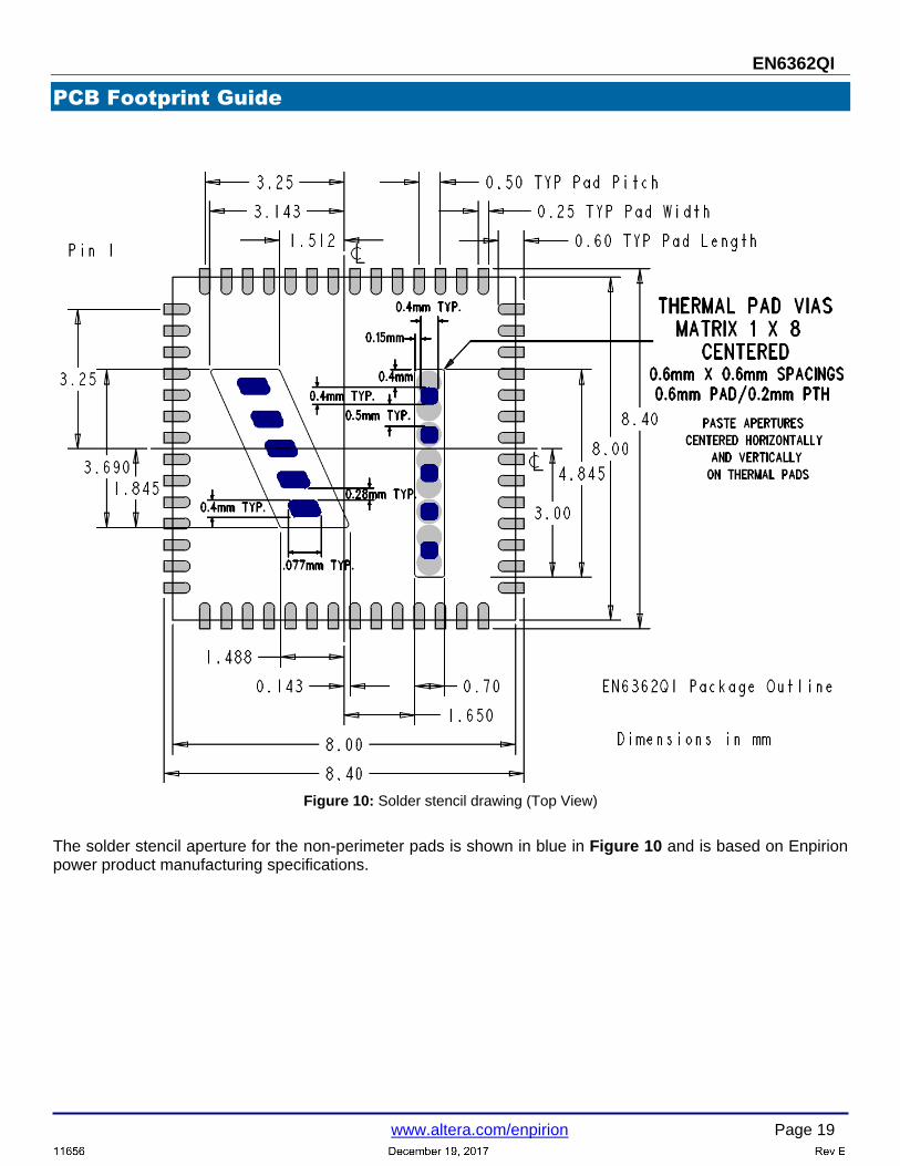
PCB Footprint Guide
Figure 10: Solder stencil drawing (Top View)
The solder stencil aperture for the non-perimeter pads is shown in blue in Figure 10 and is based on Enpirion power product manufacturing specifications.
EN6362QI
www.altera.com/enpirion Page 20
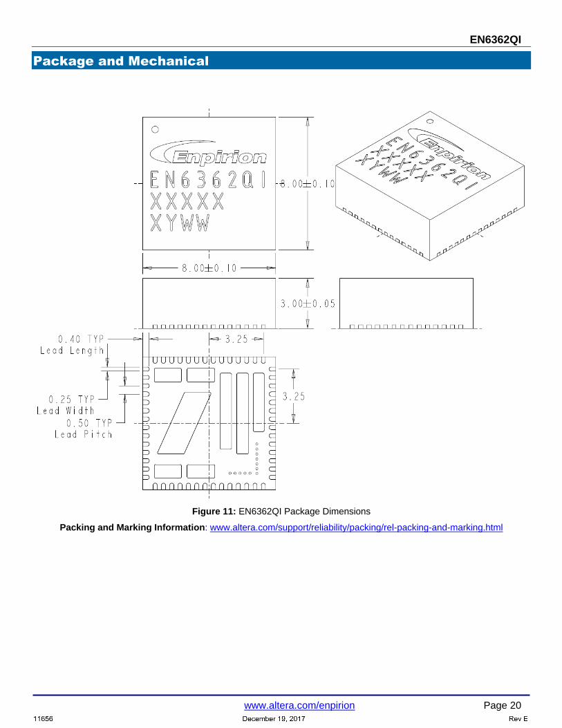
Package and Mechanical
Figure 11: EN6362QI Package Dimensions
Packing and Marking Information: www.altera.com/support/reliability/packing/rel-packing-and-marking.html

EN6362QI
www.altera.com/enpirion Page 21
Revision History
Rev Date Change(s) A Jan 2016 • Introductory production datasheet
B Oct 2016
• Modified pinout and pin description for pins 58-60
• Added performance characteristics and curves for line and load regulation, derating, EMIperformance, load transients
• Added recommendations table for compensation components
• Modified Figure 6 to show efficiency curve for Vin=5.5V, Vout=1.0V and updated equations
following it for η=88%
• Removed equation to predict to predict frequency vs Rfqadj relationship from frequencyprogramming discussion
• Modified recommended schematic and layout
• Added solder stencil drawing
• Formatting changes
C Dec 2016
• Updated total solution size from 170 mm2 to 160 mm2
• Added pin compatibility with EN6382QI on the features list
• Updated package marking on the package dimensions drawing
D Feb 2017
• Modified simplified applications schematic to show AGND-PGND connection
• Modified pin diagram to differentiate pins under the keepout area
• Updated pin description for pins 58 and 59
• Modified typical derating curve to extend up to 105⁰C
• Modified layout recommendation
• Formatting changes
E Dec 2017 • Updated Layout Recommendations section
• Updated Figures Numbers throughout document
Contact Information
Altera Corporation 101 Innovation Drive San Jose, CA 95134 Phone: 408-544-7000 www.altera.com
© 2015 Altera Corporation—Confidential. All rights reserved. ALTERA, ARRIA, CYCLONE, ENPIRION, HARDCOPY, MAX, MEGACORE, NIOS, QUARTUS and STRATIX words and logos are trademarks of Altera Corporation and registered in the U.S. Patent and Trademark Office and in other countries. All other words and logos identified as trademarks or service marks are the property of their respective holders as described at www.altera.com/common/legal.html. Altera warrants performance of its semiconductor products to current specifications in accordance with Altera's standard warranty, but reserves the right to make changes to any products and services at any time without notice. Altera assumes no responsibility or liability arising out of the application or use of any information, product, or service described herein except as expressly agreed to in writing by Altera. Altera customers are advised to obtain the latest version of device specifications before relying on any published information and before placing orders for products or services.