emerging materials challenges in microelectronics packaging
TRANSCRIPT
68 MRS BULLETIN/JANUARY 2003
Materials Issues in High-SpeedDigital Packaging
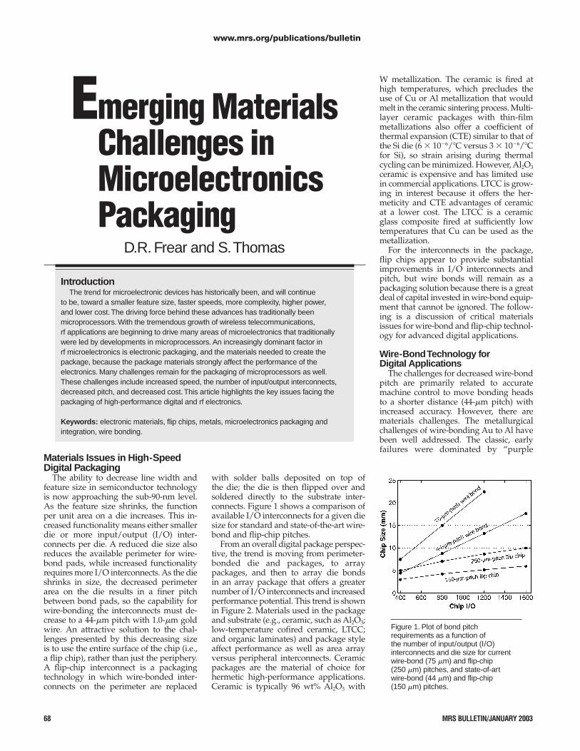
The ability to decrease line width andfeature size in semiconductor technologyis now approaching the sub-90-nm level.As the feature size shrinks, the functionper unit area on a die increases. This in-creased functionality means either smallerdie or more input/output (I/O) inter-connects per die. A reduced die size alsoreduces the available perimeter for wire-bond pads, while increased functionalityrequires more I/O interconnects. As the dieshrinks in size, the decreased perimeterarea on the die results in a finer pitchbetween bond pads, so the capability forwire-bonding the interconnects must de-crease to a 44-�m pitch with 1.0-�m goldwire. An attractive solution to the chal-lenges presented by this decreasing sizeis to use the entire surface of the chip (i.e.,a flip chip), rather than just the periphery.A flip-chip interconnect is a packagingtechnology in which wire-bonded inter-connects on the perimeter are replaced
with solder balls deposited on top ofthe die; the die is then flipped over andsoldered directly to the substrate inter-connects. Figure 1 shows a comparison ofavailable I/O interconnects for a given diesize for standard and state-of-the-art wire-bond and flip-chip pitches.
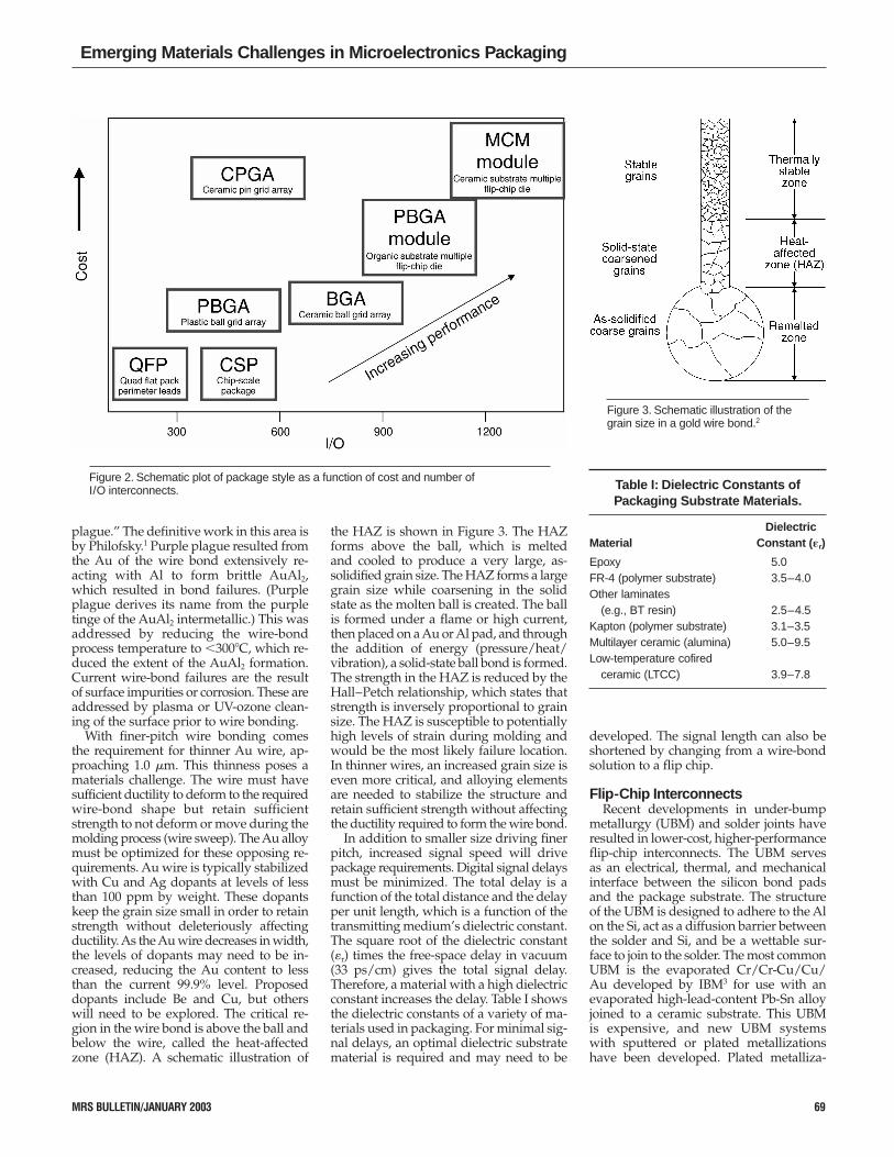
From an overall digital package perspec-tive, the trend is moving from perimeter-bonded die and packages, to arraypackages, and then to array die bondsin an array package that offers a greaternumber of I/O interconnects and increasedperformance potential. This trend is shownin Figure 2. Materials used in the packageand substrate (e.g., ceramic, such as Al2O3;low-temperature cofired ceramic, LTCC;and organic laminates) and package styleaffect performance as well as area arrayversus peripheral interconnects. Ceramicpackages are the material of choice forhermetic high-performance applications.Ceramic is typically 96 wt% Al2O3 with
W metallization. The ceramic is fired athigh temperatures, which precludes theuse of Cu or Al metallization that wouldmelt in the ceramic sintering process. Multi-layer ceramic packages with thin-filmmetallizations also offer a coefficient ofthermal expansion (CTE) similar to that ofthe Si die (6 � 10�6/�C versus 3 � 10�6/�Cfor Si), so strain arising during thermalcycling can be minimized. However, Al2O3ceramic is expensive and has limited usein commercial applications. LTCC is grow-ing in interest because it offers the her-meticity and CTE advantages of ceramicat a lower cost. The LTCC is a ceramicglass composite fired at sufficiently lowtemperatures that Cu can be used as themetallization.
For the interconnects in the package,flip chips appear to provide substantialimprovements in I/O interconnects andpitch, but wire bonds will remain as apackaging solution because there is a greatdeal of capital invested in wire-bond equip-ment that cannot be ignored. The follow-ing is a discussion of critical materialsissues for wire-bond and flip-chip technol-ogy for advanced digital applications.
Wire-Bond Technology forDigital Applications
The challenges for decreased wire-bondpitch are primarily related to accuratemachine control to move bonding headsto a shorter distance (44-�m pitch) withincreased accuracy. However, there arematerials challenges. The metallurgicalchallenges of wire-bonding Au to Al havebeen well addressed. The classic, earlyfailures were dominated by “purple
Emerging MaterialsChallenges inMicroelectronicsPackaging
D.R. Frear and S.Thomas
IntroductionThe trend for microelectronic devices has historically been, and will continue
to be, toward a smaller feature size, faster speeds, more complexity, higher power,and lower cost.The driving force behind these advances has traditionally beenmicroprocessors. With the tremendous growth of wireless telecommunications,rf applications are beginning to drive many areas of microelectronics that traditionallywere led by developments in microprocessors. An increasingly dominant factor inrf microelectronics is electronic packaging, and the materials needed to create thepackage, because the package materials strongly affect the performance of theelectronics. Many challenges remain for the packaging of microprocessors as well.These challenges include increased speed, the number of input/output interconnects,decreased pitch, and decreased cost.This article highlights the key issues facing thepackaging of high-performance digital and rf electronics.
Keywords: electronic materials, flip chips, metals, microelectronics packaging andintegration, wire bonding.
Figure 1. Plot of bond pitchrequirements as a function ofthe number of input/output (I/O)interconnects and die size for currentwire-bond (75 �m) and flip-chip(250 �m) pitches, and state-of-artwire-bond (44 �m) and flip-chip(150 �m) pitches.
www.mrs.org/publications/bulletin
Emerging Materials Challenges in Microelectronics Packaging
MRS BULLETIN/JANUARY 2003 69
plague.” The definitive work in this area isby Philofsky.1 Purple plague resulted fromthe Au of the wire bond extensively re-acting with Al to form brittle AuAl2,which resulted in bond failures. (Purpleplague derives its name from the purpletinge of the AuAl2 intermetallic.) This wasaddressed by reducing the wire-bondprocess temperature to �300�C, which re-duced the extent of the AuAl2 formation.Current wire-bond failures are the resultof surface impurities or corrosion. These areaddressed by plasma or UV-ozone clean-ing of the surface prior to wire bonding.
With finer-pitch wire bonding comesthe requirement for thinner Au wire, ap-proaching 1.0 �m. This thinness poses amaterials challenge. The wire must havesufficient ductility to deform to the requiredwire-bond shape but retain sufficientstrength to not deform or move during themolding process (wire sweep). The Au alloymust be optimized for these opposing re-quirements. Au wire is typically stabilizedwith Cu and Ag dopants at levels of lessthan 100 ppm by weight. These dopantskeep the grain size small in order to retainstrength without deleteriously affectingductility. As the Au wire decreases in width,the levels of dopants may need to be in-creased, reducing the Au content to lessthan the current 99.9% level. Proposeddopants include Be and Cu, but otherswill need to be explored. The critical re-gion in the wire bond is above the ball andbelow the wire, called the heat-affectedzone (HAZ). A schematic illustration of
the HAZ is shown in Figure 3. The HAZforms above the ball, which is meltedand cooled to produce a very large, as-solidified grain size. The HAZ forms a largegrain size while coarsening in the solidstate as the molten ball is created. The ballis formed under a flame or high current,then placed on a Au or Al pad, and throughthe addition of energy (pressure/heat/vibration), a solid-state ball bond is formed.The strength in the HAZ is reduced by theHall–Petch relationship, which states thatstrength is inversely proportional to grainsize. The HAZ is susceptible to potentiallyhigh levels of strain during molding andwould be the most likely failure location.In thinner wires, an increased grain size iseven more critical, and alloying elementsare needed to stabilize the structure andretain sufficient strength without affectingthe ductility required to form the wire bond.
In addition to smaller size driving finerpitch, increased signal speed will drivepackage requirements. Digital signal delaysmust be minimized. The total delay is afunction of the total distance and the delayper unit length, which is a function of thetransmitting medium’s dielectric constant.The square root of the dielectric constant(�r) times the free-space delay in vacuum(33 ps/cm) gives the total signal delay.Therefore, a material with a high dielectricconstant increases the delay. Table I showsthe dielectric constants of a variety of ma-terials used in packaging. For minimal sig-nal delays, an optimal dielectric substratematerial is required and may need to be
developed. The signal length can also beshortened by changing from a wire-bondsolution to a flip chip.
Flip-Chip InterconnectsRecent developments in under-bump
metallurgy (UBM) and solder joints haveresulted in lower-cost, higher-performanceflip-chip interconnects. The UBM servesas an electrical, thermal, and mechanicalinterface between the silicon bond padsand the package substrate. The structureof the UBM is designed to adhere to the Alon the Si, act as a diffusion barrier betweenthe solder and Si, and be a wettable sur-face to join to the solder. The most commonUBM is the evaporated Cr/Cr-Cu/Cu/Au developed by IBM3 for use with anevaporated high-lead-content Pb-Sn alloyjoined to a ceramic substrate. This UBMis expensive, and new UBM systemswith sputtered or plated metallizationshave been developed. Plated metalliza-
Figure 2. Schematic plot of package style as a function of cost and number ofI/O interconnects.
Figure 3. Schematic illustration of thegrain size in a gold wire bond.2
Table I: Dielectric Constants ofPackaging Substrate Materials.
Dielectric Material Constant (�r)
Epoxy 5.0FR-4 (polymer substrate) 3.5–4.0Other laminates
(e.g., BT resin) 2.5–4.5Kapton (polymer substrate) 3.1–3.5Multilayer ceramic (alumina) 5.0–9.5Low-temperature cofired
ceramic (LTCC) 3.9–7.8
70 MRS BULLETIN/JANUARY 2003
Emerging Materials Challenges in Microelectronics Packaging
tions are acknowledged to be the lowest-cost UBM.
A significant change in flip-chip inter-connects is the move toward a lower-melting-point solder alloy, such as eutectic63wt%Sn-37wt%Pb that can be processedbelow 220�C, as compared with 350�C forhigh-Pb solder. New materials on the die(low-� dielectrics) and substrate (organicmaterials) require this lower processingtemperature. The change in solder alloyalso requires a change in the UBM. Tradi-tional UBM systems are based on a thinCu layer that dissolves into high-Sn sol-ders, resulting in spalling and dewetting.Eutectic-solder UBM systems use a layerof Ni for solder wetting. The Ni is wettedby Sn-Pb solder but reacts much moreslowly than Cu. The addition of �9 wt%vanadium to nickel reduces the ferro-magnetic behavior of the Ni and enablessputtering of the Ni. Electroless plating ofNi-9wt%P is the lowest-cost UBM andhas the advantage that plating occursonly where desired on the metal pads onthe silicon. To plate onto Al, the pads arezincated to activate the surface, then im-mediately plated with Ni. One issue withNi-based UBMs is the intermetallic layerbetween the solder and Ni (Ni3Sn4). Al-though very thin, this intermetallic layercan be brittle, thus its long-term reliabilitymust be fully characterized and understood.
There are three solder-deposition tech-niques available for flip chips. Tradition-ally, high-Pb solder is evaporated onto theUBM, then it is heated above its meltingpoint, causing the solder to reflow acrossthe wettable metallization to form metal-lurgical bonds. Evaporation is expensivebecause the masks must be regularlycleaned, and there is excessive scrap solder.The composition of evaporated solder isdifficult to control outside the high-Pbregime. Solder paste is a lower-cost alter-native to evaporation and involves screen-ing the paste onto the UBM prior toreflowing. Solder paste reduces waste,cleaning is inexpensive, and the paste comesin a variety of compositions, includingeutectic Sn-Pb. The difficulty with solderpaste arises in fine-pitch applicationswhere the rheology of the paste makes itdifficult to force into the required smallholes in the screen. Solder may also beplated, which is inexpensive (no waste andeasy cleaning) and results in excellent fine-pitch coverage. Solder bumps with a pitchof 25 �m have been achieved by plating.The difficulty with plating is achievingball and compositional uniformity.
Cu and Low-� Dielectrics. New metal-lization materials are being developedon silicon devices to reduce resistance–
capacitance (R–C) delay and voltage drop,while simultaneously improving electro-migration resistance, which permits theuse of higher drive current. Plated Cu isthe lowest-cost metallization and hasgreater electrical conductivity than sputter-deposited Al metallization. Additionally,low-permittivity insulators (low-� di-electrics with � � 3) provide a potentialimprovement in R–C delays and reducecapacitance and crosstalk between conduc-tors. The low-� material is used as adielectric insulator in the interlayer di-electric (wiring the silicon out to the firstpackage interconnect) with a matrix ofCu or Al interlaced typically by using adual damascene process.4–6
The devices for which Cu and low-� di-electrics are the most suitable also requireflip-chip interconnects in order to accom-modate the large number of I/O inter-connects expected with these devices. Theflip-chip array reduces the crosstalk andR–C delays that can occur in wire-bondedpackages (the long wires can act as an-tennas and create an inductive current innearby conductors).
The move toward the use of new mate-rials like Cu and low-� dielectrics on thedie could potentially affect the manufac-turability and reliability of flip-chip pack-ages. The significant issues involved inpackaging Cu and low-� dielectrics involvebonding with the copper and the structuralstability of the dielectric during processingand in service. Many of the low-� mate-rials currently under development haveproperties that degrade at processing tem-peratures in excess of 250�C due to ex-tensive cross-linking in the polymer. Asdiscussed earlier, this requires the use oflower-melting-temperature solder andsubsequent changes in the UBM structure.Additionally, the UBM structures havebeen optimized for Al pads, and changesmay be required when Cu is implemented.Furthermore, electroless Ni is typicallypreceded by a zincation on aluminum pads,which cannot be performed on copper. Anew process must be developed to enableflip-chip bumping (deposition of solderbumps on chip bond pads) of Cu andlow-� metallizations.
Fine-Pitch Flip-Chip Interconnects. Thetrend in flip-chip interconnect pitch is forthe current 250 �m pitch to shrink to150 �m by 2004 and to 50 �m by 2010. Theforces driving this decrease in pitch lengthare the requirements for high-performancesilicon devices. These requirements includea dramatic increase in the number of I/Ointerconnects due to increases in the num-ber of signal lines and power requirements.Higher-power devices require more signal
and ground lines, and to limit point sourcesof heat, the power and ground inter-connects should be spread evenly acrossthe area array.
There are a number of materials andprocessing challenges associated with finerpitches. As the pitch shrinks, methods todeposit the solder become more limited.Solder paste is very difficult to deposit usinga silk-screen method at pitches below150 �m due to rheological limitations offorcing a semisolid (the paste) into smallholes (the silk screen). Evaporation is dif-ficult because developing a metal screenmask with the required tolerances is pro-hibitively expensive. Solder plating is stilla good option, but the solder must be veryuniform across each die. Solder-ball uni-formity is critical because large variationsbetween die could result in electrical opensfor small balls and shorts for large balls.At 250-�m pitch, ball uniformity across adie is 10%; at 150 �m, this decreases to 5%,and the change in dimension toleranceshrinks from 12.5 �m down to 3.75 �m.An additional issue with a decrease in ballsize is that the joint gap between the sub-strate and the die decreases to the pointthat it may become very difficult to flowunderfill completely under the die. At a100-�m pitch, the gap between the die andsubstrate could be significantly less than25 �m, below the limit of underfill flow.For these fine-pitch applications, an alter-native underfill technique will need to bedeveloped because flow under the chipwill not be possible. One alternative wouldbe to deposit the underfill material on thewafer immediately after flip-chip solder-bumping; then, underfill cure would si-multaneously occur during solder reflow.New underfill materials and processeswould have to be developed to implementthis alternative.
Organic Substrates for Flip Chips. Themove to organic substrates is the focus ofan extensive development effort world-wide by both printed circuit board (PCB)manufacturers and traditional materialssuppliers, one that requires significantamounts of capital. Cost savings are ex-pected by replacing ceramic with organicsubstrates. One stated reason for movingto an organic substrate is based on thebelief that, in volume production, organicmaterials are less expensive than ceramicdue to the nature of PCB processing. Or-ganic substrates also offer an increase inelectrical performance due to their lowerdielectric constant (therefore, less capaci-tance and better speed) of 3.5 for organicversus 5 for ceramics.
Advanced substrates for flip chips mustalso provide increased wireability while
Emerging Materials Challenges in Microelectronics Packaging
MRS BULLETIN/JANUARY 2003 71
delivering improved electrical performancewith reliability levels at least equivalent tocurrent surface-mounted applications. Theboard interconnect density for flip-chipsubstrates must accommodate the increas-ing density of off-chip interconnects, andcost-effective substrate capabilities thatcombine the necessary fine-line and micro-via features must be developed. Microviasare the metal-filled holes that provide aconduction path between copper lines inthe multiple layers of an organic substrate.Microvia capability must also scale withline width and spacing in order to providethe “via-in-line” structures that will be nec-essary to support bump-pitch densification.At current 250-�m pitches, microvias canbe created using a photolithographic proc-ess. At finer pitches, laser-drilling tech-niques must be developed in order to createthe required small via size to support thesmaller capture pads and facilitate thedense routing required for flip chips.
New materials with dielectric constantsapproaching 2.0 and with CTEs approach-ing 6.0 � 10�6/�C will be necessary to meetfine pitch requirements. Furthermore, uni-formity and flatness requirements must beimproved on organic substrates to ensureuniform joint size and bonding across eachdie as the interconnect pitch decreases.
The change in substrate materials drivesthe need for a lower-melting-temperaturesolder to replace the high-lead-contentSn-Pb alloys that are processed in excessof 300�C for ceramic substrates. The organicmaterials in a substrate are typically epoxy-based, and they char or burn at tempera-tures in excess of 250�C. This is similar tothe issue discussed earlier for the low-�materials proposed for the dielectric onthe silicon die. The most common solderalloy candidate is near-eutectic Sn-Pb,which can be processed below 250�C. How-ever, this could result in a situation wherethe flip-chip interconnect melts every timethat a subsequent solder reflow occurs.Multiple reflows of the solder interconnectsaccelerate intermetallic growth between thetin of the solder and the metallized padsfor the UBM and substrate. One way tocircumvent this problem is to deposit low-melting-temperature eutectic Sn-Pb solderon the substrate lands or on the high-melting-temperature solder bumps. Reflowto the substrate can be performed at eutecticSn-Pb soldering temperatures, but themixing between the high-lead-content andeutectic solders results in a higher-melting-temperature composition. Subsequentreflows, at eutectic Sn-Pb processing tem-peratures, will not remelt the “compositealloy” flip-chip joint. This addresses thelow-temperature processing requirementsfor organic substrates, but does not address
the low-� dielectric low-temperature proc-essing requirements because the high-lead-content solder must still be reflowed onthe silicon.
Lead-Free Solders. As discussed, the tra-ditional material used to create the flip-chip solder interconnect has been a Sn-Pballoy. Sn-Pb solder is used because it has arelatively low melting point, good wettingbehavior, and good electrical conductivity,and it can be used in hierarchical solder-ing. Hierarchical soldering is the utiliza-tion of a solder that has a lower meltingtemperature than all of the other solderinterconnects that precede it. The lower-temperature solder must have a workingtemperature sufficiently low that it does notmelt a higher-temperature interconnect.The melting-temperature range for Sn-Pbsolders is from 310�C for Sn-97wt%Pb to183�C for eutectic Sn-37wt%Pb. The basicrequirement of flip-chip solder inter-connects is to form a reliable electrical andmechanical connection that retains its in-tegrity through subsequent manufacturingprocesses and service conditions. The jointsmust also be able to dissipate strains gen-erated as a result of CTE mismatches underservice conditions over the lifetime of theassembly. As the number of joints increaseand their size decreases, the behavior ofsolder joints becomes problematic becausethey are more difficult to manufacture, andreliability requirements become more dif-ficult to satisfy. This is intensified for area-array applications because joints cannoteasily be viewed or inspected after assembly.
The electronics industry extensively usesPb-Sn solder alloys in flip-chip applicationsas well as in many other interconnects inelectronics packaging. However, it is wellknown that lead is a heavy-metal toxinthat can damage the kidneys, liver, blood,and central nervous system. Less than1% per year of global lead consumptionis used in solder alloys for electronic prod-ucts, but electronics and electrical systemsare becoming an increasingly larger frac-tion of landfills.7 The issue of lead leachingfrom landfills into the water table has raisedalarm as a potential source of long-termcontamination of soil and groundwater.Concerns about the presence of lead inthe environment and potential exposurescenarios that could result in the ingestionof lead by humans and wildlife haveprompted a concerted effort to limit theuse of lead in manufactured products(notably gasoline, plumbing solders, andpaint). International laws have recentlybeen proposed to expand lead controllaws to limit or ban the use of lead in manu-factured electronic products. The mostaggressive and well-known effort is the
European Union’s Waste in Electrical andElectronic Equipment (WEEE) directive,which proposes a ban on lead in electron-ics by 2006. The Japanese EnvironmentalAgency has proposed that lead-containingscrap must be disposed of in sealed land-fills to prevent leaching. The JapaneseMinistry of International Trade and Indus-try and the Japan Automobile IndustriesAssociation called for a 50% reduction oflead in vehicles (excluding batteries) by2001 (which was achieved) and a two-thirds reduction by 2003.8
Electronics manufacturers have re-sponded to these proposed bans in a varietyof ways. Many companies have not takena stance, hoping that legislation will notbe enacted. Other companies have aggres-sively pursued solutions to the proposedbans and are using lead-free products asa “green” marketing strategy. Extensiveresearch on lead-free solders has beenpublished. A comprehensive review ofthe status of lead-free solders can be foundin the literature that is primarily focusedon carrier-to-board (surface-mounted andthrough-hole) interconnects.9–21 A growingrequirement is lead-free solders for flip-chip interconnects.
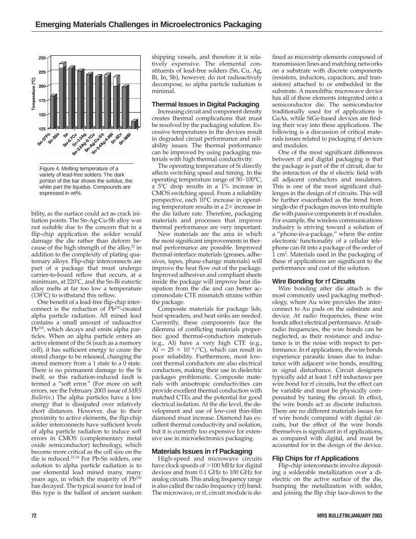
Lead-free solders for electronics appli-cations are based on Sn-rich compoundsthat fall into a melting-temperature rangesimilar to the traditional eutectic Pb-Snsolder alloys (183�C). These include eutecticSn-3.5wt%Ag with alloying elements ofBi, Cu, Sb, In, or Zn. Other alloys based onthe Sn-Cu, Sn-In, Sn-Sb, Sn-Bi, and Sn-Znsystems have also been proposed. A smalltwo-phase region (temperature differencebetween liquidus and solidus) is desirablebecause it prevents the joint from movingand becoming disturbed during solidifica-tion. Binary or ternary near-eutectic alloysare also desirable because simpler alloysreduce the potential for compositionalvariations that affect the behavior of thesolder joint. A graph of the melting tem-peratures of potential solder alloys is shownin Figure 4. The alloys Sn-0.7wt%Cu, Sn-3.5wt%Ag, and Sn-3.8wt%Ag-0.7wt%Cuare the most promising lead-free flip-chipsolder alloys, based on the given criteria.The Sn-Sb alloy was deemed to have toolarge a two-phase region, and its liquidustemperature of 240�C was too high for chipattachment to organic substrates (a proc-ess temperature of 245�C is desired). TheSn-Zn alloy had too many processing dif-ficulties due to the rapid oxidation behaviorof the Zn in the molten state and thecorrosion susceptibility of the alloy aftersolidification. The Sn-Ag-Bi alloy had toolarge a two-phase region that could resultin a disturbed solder joint (very rough,dull surface of the solder) and affect relia-
72 MRS BULLETIN/JANUARY 2003
Emerging Materials Challenges in Microelectronics Packaging
bility, as the surface could act as crack ini-tiation points. The Sn-Ag-Cu-Sb alloy wasnot suitable due to the concern that in aflip-chip application the solder woulddamage the die rather than deform be-cause of the high strength of the alloy,22 inaddition to the complexity of plating qua-ternary alloys. Flip-chip interconnects arepart of a package that must undergocarrier-to-board reflow that occurs, at aminimum, at 220�C, and the Sn-Bi eutecticalloy melts at far too low a temperature(138�C) to withstand this reflow.
One benefit of a lead-free flip-chip inter-connect is the reduction of Pb210-createdalpha particle radiation. All mined leadcontains a small amount of radioactivePb210, which decays and emits alpha par-ticles. When an alpha particle enters anactive element of the Si (such as a memorycell), it has sufficient energy to cause thestored charge to be released, changing thestored memory from a 1 state to a 0 state.There is no permanent damage to the Siitself, so this radiation-induced fault istermed a “soft error.” (For more on softerrors, see the February 2003 issue of MRSBulletin.) The alpha particles have a lowenergy that is dissipated over relativelyshort distances. However, due to theirproximity to active elements, the flip-chipsolder interconnects have sufficient levelsof alpha particle radiation to induce softerrors in CMOS (complementary metaloxide semiconductor) technology, whichbecome more critical as the cell size on thedie is reduced.23,24 For Pb-Sn solders, onesolution to alpha particle radiation is touse elemental lead mined many, manyyears ago, in which the majority of Pb210
has decayed. The typical source for lead ofthis type is the ballast of ancient sunken
shipping vessels, and therefore it is rela-tively expensive. The elemental con-stituents of lead-free solders (Sn, Cu, Ag,Bi, In, Sb), however, do not radioactivelydecompose, so alpha particle radiation isminimal.
Thermal Issues in Digital PackagingIncreasing circuit and component density
creates thermal complications that mustbe resolved by the packaging solution. Ex-cessive temperatures in the devices resultin degraded circuit performance and reli-ability issues. The thermal performancecan be improved by using packaging ma-terials with high thermal conductivity.
The operating temperature of Si directlyaffects switching speed and timing. In theoperating temperature range of 50–100�C,a 5�C drop results in a 1% increase inCMOS switching speed. From a reliabilityperspective, each 10�C increase in operat-ing temperature results in a 2� increase inthe die failure rate. Therefore, packagingmaterials and processes that improvethermal performance are very important.
New materials are the area in whichthe most significant improvements in ther-mal performance are possible. Improvedthermal-interface materials (greases, adhe-sives, tapes, phase-change materials) willimprove the heat flow out of the package.Improved adhesives and compliant sheetsinside the package will improve heat dis-sipation from the die and can better ac-commodate CTE mismatch strains withinthe package.
Composite materials for package lids,heat spreaders, and heat sinks are needed.Currently, these components face thedilemma of conflicting materials proper-ties: good thermal-conduction materials(e.g., Al) have a very high CTE (e.g.,Al � 25 � 10�6/�C), which can result inpoor reliability. Furthermore, most low-cost thermal conductors are also electricalconductors, making their use in dielectricpackages problematic. Composite mate-rials with anisotropic conductivities canprovide excellent thermal conduction withmatched CTEs and the potential for goodelectrical isolation. At the die level, the de-velopment and use of low-cost thin-filmdiamond must increase. Diamond has ex-cellent thermal conductivity and isolation,but it is currently too expensive for exten-sive use in microelectronics packaging.
Materials Issues in rf PackagingHigh-speed and microwave circuits
have clock speeds of �100 MHz for digitaldevices and from 0.1 GHz to 100 GHz foranalog circuits. This analog frequency rangeis also called the radio frequency (rf) band.The microwave, or rf, circuit module is de-
fined as microstrip elements composed oftransmission lines and matching networkson a substrate with discrete components(resistors, inductors, capacitors, and tran-sistors) attached to or embedded in thesubstrate. A monolithic microwave devicehas all of these elements integrated onto asemiconductor die. The semiconductortraditionally used for rf applications isGaAs, while SiGe-based devices are find-ing their way into these applications. Thefollowing is a discussion of critical mate-rials issues related to packaging rf devicesand modules.
One of the most significant differencesbetween rf and digital packaging is thatthe package is part of the rf circuit, due tothe interaction of the rf electric field withall adjacent conductors and insulators.This is one of the most significant chal-lenges in the design of rf circuits. This willbe further exacerbated as the trend fromsingle-die rf packages moves into multipledie with passive components in rf modules.For example, the wireless communicationsindustry is striving toward a solution ofa “phone-in-a-package,” where the entireelectronic functionality of a cellular tele-phone can fit into a package of the order of1 cm2. Materials used in the packaging ofthese rf applications are significant to theperformance and cost of the solution.
Wire Bonding for rf CircuitsWire bonding after die attach is the
most commonly used packaging method-ology, where Au wire provides the inter-connect to Au pads on the substrate anddevice. At radio frequencies, these wirebonds affect electrical performance. At sub-radio frequencies, the wire bonds can beneglected, as their resistance and induc-tance is in the noise with respect to per-formance. In rf applications, the wire bondsexperience parasitic losses due to induc-tance with adjacent wire bonds, resultingin signal disturbance. Circuit designerstypically add at least 1 nH inductance perwire bond for rf circuits, but the effect canbe variable and must be physically com-pensated by tuning the circuit. In effect,the wire bonds act as discrete inductors.There are no different materials issues forrf wire bonds compared with digital cir-cuits, but the effect of the wire bondsthemselves is significant in rf applications,as compared with digital, and must beaccounted for in the design of the device.
Flip Chips for rf ApplicationsFlip-chip interconnects involve deposit-
ing a solderable metallization over a di-electric on the active surface of the die,bumping the metallization with solder,and joining the flip chip face-down to the
Figure 4. Melting temperature of avariety of lead-free solders.The darkportion of the bar shows the solidus, thewhite part the liquidus. Compounds areexpressed in wt%.
Emerging Materials Challenges in Microelectronics Packaging
MRS BULLETIN/JANUARY 2003 73
substrate. Flip chips provide substantialimprovements in off-circuit rf performancesince the inductance is decreased becausethe ball height and shape are very consis-tent and predictable. Wire-bond lengthscan vary (typically 100 �m), resulting inparasitic variations not observed in flip-chip interconnects. The number of I/Ointerconnects on an rf circuit is generallysmall, so the pitch of the interconnects isgenerally quite large.
The die interconnects on GaAs are typi-cally Au, whereas on Si, they are Al. AUBM is required for Si applications be-cause solder does not wet Al. The solderwould wet the Au of the GaAs, but the Aulayer is very thin and would dissolve veryquickly, so a UBM is also required forGaAs. The UBMs available for Si can alsobe applied to GaAs but can be simplerbecause the adhesion of other metals toAu is easier to achieve than it is on Al.
The solder alloys for GaAs flip-chipsolder bumps tend to be similar to thosefor Si, but with a greater emphasis onAu-based alloys because of the desire touse a highly conductive material such asAu for very high-speed applications.Eutectic Au-Sn, Ag, and In alloys have com-monly been used, but the wetting of thesesolders is typically poor. For finer-pitchapplications on GaAs (due to small diesize, not large numbers of I/O inter-connects), other materials with good wettingcharacteristics are needed. Conductiveadhesives have been explored for GaAsbumps. Work by Lin et al.25 found no sig-nificant difference in electrical perform-ance up to 2 GHz between a conductiveadhesive and Au-Sn solder. The use ofunderfill for flip-chip packages can causea major loss in rf energy because the di-electric constant of the underfill polymeris greater than that of air. With a conduc-tive adhesive localized to just the bondpads, not the entire surface of the die, thisrf loss is not observed.
Substrate Materials for rf CircuitsOptimum electrical performance is
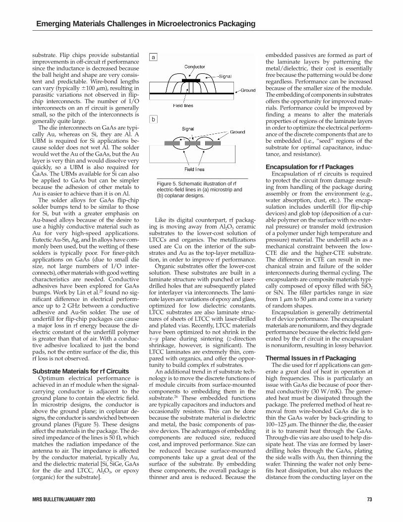
achieved in an rf module when the signal-carrying conductor is adjacent to theground plane to contain the electric field.In microstrip designs, the conductor isabove the ground plane; in coplanar de-signs, the conductor is sandwiched betweenground planes (Figure 5). These designsaffect the materials in the package. The de-sired impedance of the lines is 50 , whichmatches the radiation impedance of theantenna to air. The impedance is affectedby the conductor material, typically Au,and the dielectric material [Si, SiGe, GaAsfor the die and LTCC, Al2O3, or epoxy(organic) for the substrate].
Like its digital counterpart, rf packag-ing is moving away from Al2O3 ceramicsubstrates to the lower-cost solution ofLTCCs and organics. The metallizationsused are Cu on the interior of the sub-strates and Au as the top-layer metalliza-tion, in order to improve rf performance.
Organic substrates offer the lower-costsolution. These substrates are built in alaminate structure with punched or laser-drilled holes that are subsequently platedfor interlayer via interconnects. The lami-nate layers are variations of epoxy and glass,optimized for low dielectric constants.LTCC substrates are also laminate struc-tures of sheets of LTCC with laser-drilledand plated vias. Recently, LTCC materialshave been optimized to not shrink in thex–y plane during sintering (z-directionshrinkage, however, is significant). TheLTCC laminates are extremely thin, com-pared with organics, and offer the oppor-tunity to build complex rf substrates.
An additional trend in rf substrate tech-nology is to move the discrete functions ofrf module circuits from surface-mountedcomponents to embedding them in thesubstrate.26 These embedded functionsare typically capacitors and inductors andoccasionally resistors. This can be donebecause the substrate material is dielectricand metal, the basic components of pas-sive devices. The advantages of embeddingcomponents are reduced size, reducedcost, and improved performance. Size canbe reduced because surface-mountedcomponents take up a great deal of thesurface of the substrate. By embeddingthese components, the overall package isthinner and area is reduced. Because the
embedded passives are formed as part ofthe laminate layers by patterning themetal/dielectric, their cost is essentiallyfree because the patterning would be doneregardless. Performance can be increasedbecause of the smaller size of the module.The embedding of components in substratesoffers the opportunity for improved mate-rials. Performance could be improved byfinding a means to alter the materialsproperties of regions of the laminate layersin order to optimize the electrical perform-ance of the discrete components that are tobe embedded (i.e., “seed” regions of thesubstrate for optimal capacitance, induc-tance, and resistance).
Encapsulation for rf PackagesEncapsulation of rf circuits is required
to protect the circuit from damage result-ing from handling of the package duringassembly or from the environment (e.g.,water absorption, dust, etc.). The encap-sulation includes underfill (for flip-chipdevices) and glob top (deposition of a cur-able polymer on the surface with no exter-nal pressure) or transfer mold (extrusionof a polymer under high temperature andpressure) material. The underfill acts as amechanical constraint between the low-CTE die and the higher-CTE substrate.The difference in CTE can result in me-chanical strain and failure of the solderinterconnects during thermal cycling. Theencapsulants are composite materials typi-cally composed of epoxy filled with SiO2or SiN. The filler particles range in sizefrom 1 �m to 50 �m and come in a varietyof random shapes.
Encapsulation is generally detrimentalto rf device performance. The encapsulantmaterials are nonuniform, and they degradeperformance because the electric field gen-erated by the rf circuit in the encapsulantis nonuniform, resulting in lossy behavior.
Thermal Issues in rf PackagingThe die used for rf applications can gen-
erate a great deal of heat in operation athigh frequencies. This is particularly anissue with GaAs die because of poor ther-mal conductivity (30 W/mK). The gener-ated heat must be dissipated through thepackage. The preferred method of heat re-moval from wire-bonded GaAs die is tothin the GaAs wafer by back-grinding to100–125 �m. The thinner the die, the easierit is to transmit heat through the GaAs.Through-die vias are also used to help dis-sipate heat. The vias are formed by laser-drilling holes through the GaAs, platingthe side walls with Au, then thinning thewafer. Thinning the wafer not only bene-fits heat dissipation, but also reduces thedistance from the conducting layer on the
Figure 5. Schematic illustration of rfelectric-field lines in (a) microstrip and(b) coplanar designs.
Emerging Materials Challenges in Microelectronics Packaging
surface of the die to the ground plane onthe die back side, which improves impe-dance match in microstrip designs.
Issues with through-die vias and waferthinning are cost and die breakage. Laserdrilling and thinning increase the cost ofthe die. Furthermore, GaAs is a very brittlematerial, and the presence of vias andthinning exacerbates potential cracking.
One method for reducing the thermaland mechanical problems associated withthermal issues on GaAs is to use flip-chipinterconnects. In flip chips, the bumps actas electrical, mechanical, and thermal inter-connects. The bumps are on the front sideof the die, so full-thickness die can beused. The challenge with using a flip chipas a thermal conductor is putting a suffi-cient number of bumps on the die to dis-sipate the heat.
ConclusionsMaterials development is one of the
most important aspects of microelectronicspackaging. The need for new materials tobe developed to meet the requirements forhigh-speed digital and rf applications dis-cussed in this article is clear. Considerable
resources are required to develop andcharacterize these materials. These mate-rials must also be tested to determine theircompatibility with assembly processes anddevice performance and to meet industrystandards. The fundamental materialscharacteristics that must be understood,depending upon the material, includedielectric constant, dielectric loss, con-ductivity, resistivity, moisture absorption,glass-transition temperature, strength,time-dependent deformation (creep), andfracture toughness.
References1. E. Philofsky, Solid-State Electron. 13 (1970)p. 1391.2. L. Levine and M. Sheaffer, Solid State Technol.36 (March 1993) p. 63.3. L.S. Goldman, IBM J. Res. Dev. 13 (1969)p. 251.4. K.J. Blackwell, I.I. Memis, and R.P. Kuracina,High Density Interconnect—HDI 1 (4) (1998)p. 20.5. P.C. Andricacos, C. Uzoh, J.O. Dukovic,J. Horkans, and H. Deligianni, IBM J. Res. Dev.42 (1998) p. 567.6. C.-K. Hu and J.M.E. Harper, Mater. Chem.Phys. 52 (1998) p. 5.
7. N.C. Lee, Adv. Microelectron. (September/October 1999) p. 29.8. A. Grusd, in Circuits Assembly 10 (8) (1999)p. 32.9. J. Glazer, Int. Mater. Rev. 40 (2) (1995) p. 65.10. J. Glazer, J. Electron. Mater. 23 (8) (1994)p. 693.11. G. Whitten, in Proc. 50th Electronic Compo-nents and Technology Conf. (Institute of Electricaland Electronics Engineers, Piscataway, NJ,2000) p. 1410.12. E. Bradley III and J. Hramisavljevic, in Proc.50th Electronic Components and Technology Conf.(Institute of Electrical and Electronics Engineers,Piscataway, NJ, 2000) p. 1443.13. W.K. Choi and H.M. Lee, J. Electron. Mater.29 (10) (2000) p. 1207.14. F. Guo, S. Choi, J.P. Lucas, and K.N.Subramanian, J. Electron. Mater. 29 (10) (2000)p. 1241.15. T.S. Choi, K.N. Subramanian, and J.P.Lucas, J. Electron. Mater. 29 (10) (2000) p. 1249.16. Y. Miyazawa and T. Ariga, in Proc. 1stInt. Symp. on Environmentally Conscious Design(IEEE Computer Society, Los Alamitos, CA,1999) p. 616.17. M. Abtew and G. Selvardery, Mater. Sci.Eng. 27 (2000) p. 95.18. H.K. Seelig and D. Suraski, in Proc. 50thElectronic Components and Technology Conf. (In-stitute of Electrical and Electronics Engineers,Piscataway, NJ, 2000) p. 1405.19. K.G. Snowden, C.G. Tanner, and J.R.Thompson, in Proc. 50th Electronic Componentsand Technology Conf. (Institute of Electrical andElectronics Engineers, Piscataway, NJ, 2000)p. 1416.20. T.M. Korhonen, P. Su, S.J. Hong, and M.A.Korhonen, J. Electron. Mater. 29 (10) (2000)p. 1194.21. J.C. Foley, A. Gickler, F.H. Leprevost, and D.Brown, J. Electron. Mater. 29 (10) (2000) p. 1258.22. D.R. Frear and P.T. Vianco, Metall. Trans.25A (1994) p. 1509.23. M.W. Roberson, P.A. Deane, S. Bonafede,A. Huffman, and S. Nangalia, J. Electron. Mater.29 (10) (2000) p. 1274.24. Z. Hasnain and A. Ditali, in 30th Annu. Proc.on Reliability Physics (IRPS Publication Services,Westmoreland, NY, 1992) p. 276.25. J.K. Lin, B. Lytle, J. Drye, T. Scharr, R. Sharma,and R. Subrahmanyan, in Proc. 46th ElectronicComponents and Technology Conf. (Institute ofElectrical and Electronics Engineers, Piscataway,NJ, 1996) p. 1059.26. P. Bowles and L. Li, in Proc. IMAPS Adv.Technol. Workshop on Passive Integration (Interna-tional Microelectronics and Packaging Society,Washington, DC, 2002) p. 71. ■■
Achieve accurate,repeatable results
S y s t e m S o l u t i o n s
Process Microelectronic Devices& Opto-electronic Materials
Logitech LimitedErskine Ferry Road, Old Kilpatrick,Glasgow G60 5EU, Scotland, UK
Tel: +44 (0) 1389 875444Fax: +44 (0) 1389 879042Fax: +44 (0) 1389 890956 (Sales)e-mail: [email protected]
www.logitech.uk.com
Specialised device & component processing systems fordelicate cutting � dicing � bonding � lapping � polishing �CMP operations.
� Process difficult ceramic materials for use in LTCC technology.� Silicon & III-V semiconductor based wafer & device polishing.� Delayering of MEMS devices for Fault Analysis & Reverse
Engineering.� Planarization of Silicon Thermal Oxide and Nitride layers.� CMP processing to EPI ready surface quality.
See us at Photonics West, booth 1006
74 MRS BULLETIN/JANUARY 2003
For more information, see www.mrs.org/publications/bulletin/advertisers/2003/jan/.
MRS Bulletin online:MRS Bulletin online:www.mrs.org/publications/
bulletin
www.mrs.org/publications/bulletin