embedded microcontroller based … · web viewthe proportionality constant between input and output...
TRANSCRIPT

ABSTRACT
ABSTRACT
Audiometry is the technique to identify and quantitatively
determine the degree of hearing loss of a person by measuring his or her
hearing sensitivity, so that suitable medical treatment or one of the
appropriate hearing aids and assistive devices can be prescribed. In
audiological investigations, the hearing sensitivity is tested for pure tones,
speech or other sound stimuli. The result, when plotted graphically, is called
an audiogram. The electronic instrument used for measuring the hearing
threshold level is called an audiometer. Using it, the test tones of different
frequencies and levels are generated and presented to the patient and hearing
thresholds are determined on the basis of patient’s response. The auditory
system and its disorders are described. Audiometric test is discussed.
TABLE OF CONTENTS
CHAPTER NO. TITLE PAGE NO.
ABSTRACT v
LIST OF TABLE ix
LIST OF FIGURES x
1. INTRODUCTION 1
1.1 ABOUT THE PROJECT 1
1.2 ORGANIZATION PROFILE 3
2. PHYSIOLOGY OF THE AUDITORY SYSTEM 4
2.1 CAUSES FOR HEARING LOSS
6
3. HEARING TESTS 8
3.1 PURE TONE AIR CONDUCTION
THRESHOLD TESTING 9
3.2 REPRESENTATION OF SOUND 10
3.3 AUDIOGRAM 10
4. BLOCK DIAGRAM OF THE AUDIOMETER 14
4.1 BLOCK DIAGRAM DESCRIPTION 15
5. HARDWARE 16
5.1 POWER SUPPLY 16
5.1.1 Linear Mode Power Supply 16
5.2 FUNCTION GENERATOR 19
5.2.1 Circuit Description 22
5.2.1.1 Setting Up 23

5.2.2 IC 8038 Description 23
5.2.2.1 Features 23
5.3 PRE AMPLIFIER 25
5.3.1 Circuit Description 26
5.3.2 IC LM324 Description 27
5.3.2.1 Features 27
5.3.2.2 Unique Characteristics 28
5.3.2.3 Advantages 28
5.4 POWER AMPLIFIER 29
5.4.1 Circuit Description 30
5.4.2 IC LM386 Description 31
5.4.2.1 Features 31
5.5 ATTENUATOR CONTROL 32
5.6 HEADPHONE 34
5.7 CLAMPER CIRCUIT 35
5.7.1 Positive Clamper 35
5.8 ADC 37
5.8.1 Successive Approximation ADC 38
5.8.1.1 Operation 39
5.8.2 Connection Diagram of ADC0804 42
5.8.3 IC ADC0804 Description 43
5.8.3.1 Features 43
6. SOFTWARE 44
6.1 INTRODUCTION TO EMBEDDED SYSTEM 44
6.2 IC 89C51 MICROCONTROLLER 45
6.2.1 Features 46
6.2.2 Description 46
7. LIQUID CRYSTAL DISPLAY 48
8. CONCLUSION 49
9. APPENDICIES 50
9.1 APPENDIX 1 50
9.2 APPENDIX 2 51
9.3 APPENDIX 3 59
10. REFERENCES 82
LIST OF TABLES
NO. TITLE PAGE NO.
1. Relation between Hearing Thresholds and
Degree of Hearing Loss (for adults) 13
2. Relation between Regulator Names and its
Output Voltages 18
3. Details of IC 89C51 45
LIST OF FIGURES
NO. TITLE PAGE NO.
1. The organ of hearing 5
2. Audiogram of normal ears and impaired ears 11
3. Block diagram of
Embedded Microcontroller based Audiometry 14
4. Basic building block of Linear Mode Power Supply 17
5. Power Supply 18
6. Function Generator 21
7. Pre Amplifier Stage 26
8. Power Amplifier 30
9. Band Pass Filter 32
10. Frequency Response – Band Pass Filter 33
11. Clamper Circuit 35
12. Clamping a Waveform 36
13. Block diagram of
Successive Approximation A/D converter 38
14. Illustration of conversion process 41
15. Connection Diagram of ADC0804 42
INTRODUCTION
1. INTRODUCTION
1.1. ABOUT THE PROJECT
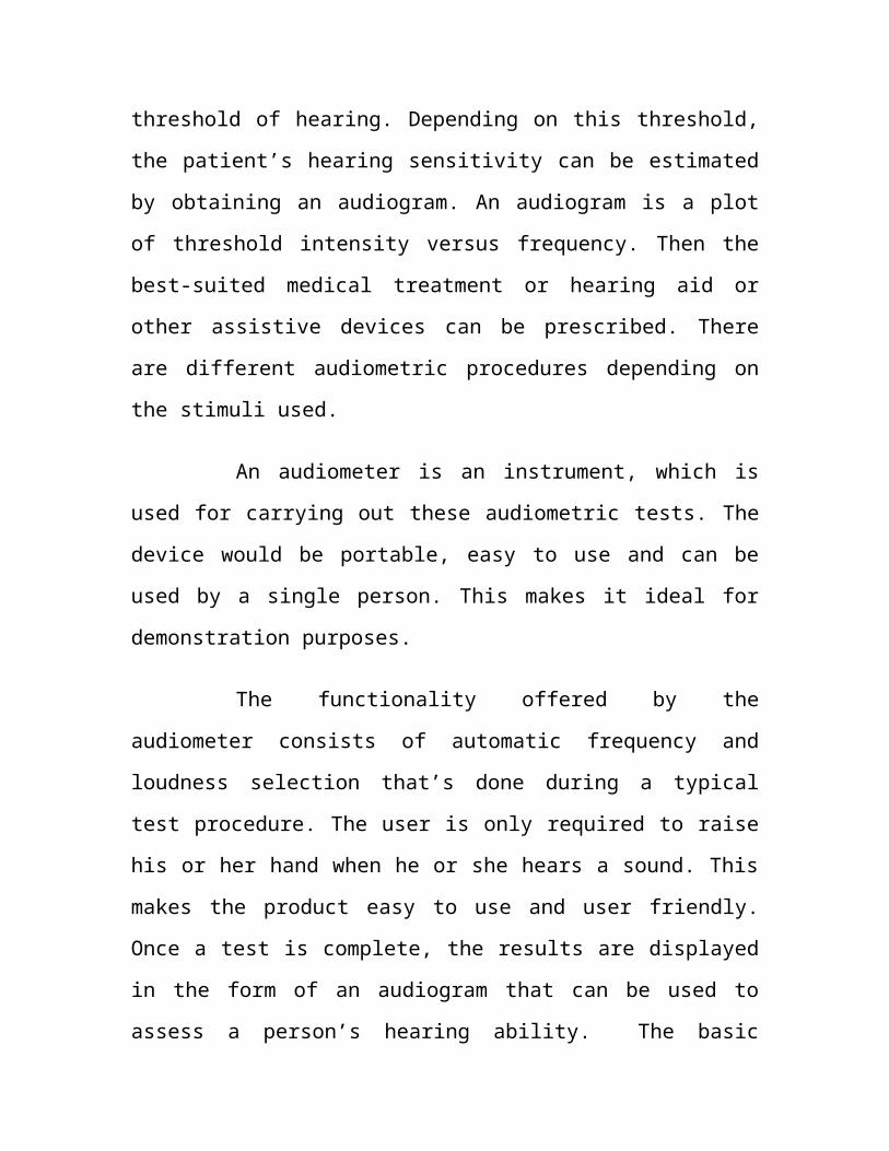
There could be various disorders in the various parts of the ear.
Audiological investigations help us to diagnose the nature of deafness and
localize the site of disorder. The method by which patient's hearing
sensitivity can be determined is termed as audiometry. It helps in assessing
the nature, degree, and probable cause of the hearing impairment. In this
technique, auditory stimuli with varying intensity levels are presented to the
person who responds to these stimuli. The minimum intensity level of these
stimuli to which consistent responses are obtained is taken as the threshold
of hearing. Depending on this threshold, the patient’s hearing sensitivity can
be estimated by obtaining an audiogram. An audiogram is a plot of threshold
intensity versus frequency. Then the best-suited medical treatment or
hearing aid or other assistive devices can be prescribed. There are different
audiometric procedures depending on the stimuli used.
An audiometer is an instrument, which is used for carrying out
these audiometric tests. The device would be portable, easy to use and can
be used by a single person. This makes it ideal for demonstration purposes.
The functionality offered by the audiometer consists of
automatic frequency and loudness selection that’s done during a typical test
procedure. The user is only required to raise his or her hand when he or she
hears a sound. This makes the product easy to use and user friendly. Once a
test is complete, the results are displayed in the form of an audiogram that
can be used to assess a person’s hearing ability. The basic functionality of
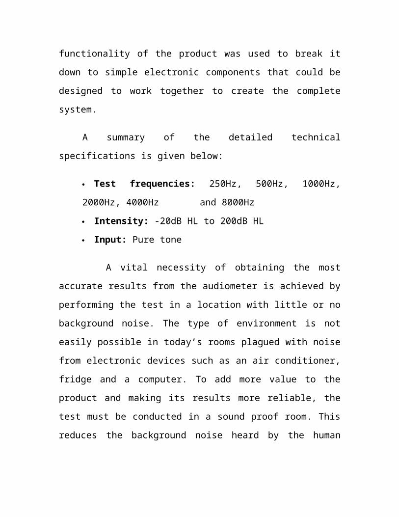
the product was used to break it down to simple electronic components that
could be designed to work together to create the complete system.
A summary of the detailed technical specifications is given below:
Test frequencies: 250Hz, 500Hz, 1000Hz, 2000Hz, 4000Hz
and 8000Hz
Intensity: -20dB HL to 200dB HL
Input: Pure tone
A vital necessity of obtaining the most accurate results from the
audiometer is achieved by performing the test in a location with little or no
background noise. The type of environment is not easily possible in today’s
rooms plagued with noise from electronic devices such as an air conditioner,
fridge and a computer. To add more value to the product and making its
results more reliable, the test must be conducted in a sound proof room. This
reduces the background noise heard by the human ear. This feature makes
the product more desirable, hence enhancing the overall system.
This report deals with the detailed electronic circuit diagrams
and the practical application of the audiometer.
1.1. ORGANAIZATION PROFILE
Electronic Engineering Corporation is a leading Indian
Manufacturer of a wide range of bio-medical electronic instruments and
scientific pumps.
With over a decade of experience and service to the scientific
and medical profession, EEC's products are acknowledged for excellent
performance and long-term reliability.
These medical and scientific instruments are used by reputed
medical professionals and scientists in many clinics, hospitals government
organizations, defense establishments, educational institutions and research
laboratories. Rigid quality control and utmost care is exercised in the
selection of materials that go into each instrument. All products are futurist
in design and specially built to withstand rigorous use. Common features of
these instruments are latest technology, high reliability components,
compact design and simple operation.

The Registered Office and Factory details are as follows:-
Address
Electronic Engineering Corporation,
T-4, Dr.Vikram Sarabai Instronic Estate,
Chennai – 600 041, Tamilnadu, India.
Telephone Numbers : 091 - 044 - 4925853
091 - 044 - 4481680
Fax : 091 - 044 - 4925853
E-Mail : [email protected]
Website : www.eec-india.com
PHYSIOLOGY OF THE
AUDITORY SYSTEM
2. PHYSIOLOGY OF AUDITORY SYSTEM
Fig.1. The organ of hearing
The ear consists of three basic parts - the outer ear, the middle
ear, and the inner ear. Each part of the ear serves a specific purpose in the
task of detecting and interpreting sound. The outer ear serves to collect and
channel sound to the middle ear. The middle ear serves to transform the
energy of a sound wave into the internal vibrations of the bone structure of
the middle ear and ultimately transform these vibrations into a compression
wave in the inner ear. The inner ear serves to transform the energy of a
compression wave within the inner ear fluid into nerve impulses which can
be transmitted to the brain.
Generally, the lowest sound level that people of excellent
hearing can discern has an acoustic sound power about 10-12 W, 0 dB
The loudest sound generally encountered is that of a jet aircraft
with a sound power of 105 W, 170 dB.
2.1. CAUSES FOR HEARING LOSS
Each section of the ear has diseases specific to it and specific
tests (investigations) are there to identify disorders in each portion. The
common cause of disorder in the external auditory meatus is collection of
either wax or fungal debris or foreign body in it. To diagnose this no
investigation is required and your doctor can see it directly and clean it with
instruments. This deafness due to blockage of the external ear is usually very
slight.
The middle ear comprises of the eardrum, the ossicles, and the
air space within the cavity of the middle ear. The common diseases affecting
this portion are perforation in the ear drum, a stiffness or damage to the
chain of small bones in the ear, and collection of fluid in the middle ear
space (called middle ear effusion). A perforation can usually be diagnosed
just by visualizing the ear-drum; however the other middle ear disorders
require special investigations for confirmation.
The disease of the inner ear, i.e. the cochlea is difficult to treat.
Disorders of the inner ear not only causes a deafness called sensorineural
(perceptive) deafness but also may case a peculiar sensation of buzzing
sounds in the ear called tinnitus. Deafness due to disorders of the inner ear is
commonly refractory to medical and surgical methods and usually hearing
aids are the only option. Deafness may also occur due to diseases of the
nerve carrying the sensation from the cochlea to the brain. Deafness due to
disorder of the nerve is called retrocochlear deafness and deafness due to
disorders of the nerves which carry the sensation of hearing still higher up to
auditory cortex are called central deafness.
The common symptoms of disorders in the auditory system are
difficulty in hearing normal conversation from a distance of 8 feet or a
whisper from a distance of 3 feet, can hear people talk but have difficulty in
understanding what they say i.e. spoken word appear jumbled up, hear
comparatively less in one ear, require to raise the volume of which is
uncomfortable to other people, hear whistling/buzzing sounds in the ear or in
the head when actually such sounds are not there, have a sensation of
blockage/heaviness in one or both ears.
HEARING TESTS
3. HEARING TESTS
Hearing test helps to detect hearing loss, identify how severe it
is, and determine what is causing it. It also measures the ability of sound to
reach the brain. Sounds are actually vibrations of different frequencies and
intensities in the air around us; air in the ear canals and bones in the ears and
skull helps these vibrations to travel from the ear to the brain, where we
"hear" them. By measuring our ability to hear sounds that reach the inner ear
through the ear canal (air-conducted sounds) and sounds transmitted through
bones (bone-conducted sounds), hearing tests helps us to determine what
kind of hearing loss we have.
Most hearing tests require a response to a series of tones or
words. These tests include:
Whispered speech testing, which is a simple screening test that
assesses our ability to hear whispered speech across a short distance.
Pure tone audiometry, which measures our ability to hear sounds that
reach the inner ear through the ear canal (air conduction). By using
vibrations, this test can also measure hearing through bone (bone
conduction).
Tuning fork testing, this assesses how well the sound moves through
our ear.
Speech reception and word recognition testing, which measure our
ability to hear and understand speech.

An ear examination may be done:
As part of a routine physical examination.
To screen infants and children for hearing loss.
To determine the cause of symptoms such as earache, a feeling of
pressure or fullness in the ear, or hearing loss.
To detect excess wax or a foreign object in the ear canal.
To detect the location of an ear infection. The infection may involve
only the external ear canal (otitis externa) or the middle ear behind the
eardrum (otitis media or otitis media with effusion).
To monitor the effectiveness of treatment for an ear problem.
3.1. PURE TONE AIR CONDUCTION THRESHOLD TESTING
To assess sensitivity, a series of 0.5 s bursts of single-frequency
stimuli are presented to the subject through calibrated earphones worn on the
head. The subject is requested to respond (by hand raising or button pushing)
each time a beep is heard, even if it is faint. Pure tone testing is performed
separately for each ear and for frequencies from 250 to 8000 Hz. The
audiometer attenuator is adjusted until the person responds correctly to 50%
of the test beeps presented. The smallest increment step on the attenuator is
usually 5 dB. The threshold (50% correct responses) is recorded on the
audiogram using a (red) “o” for the right ear and a (blue) “x” for the left ear.
The test signal passes through the outer ear, the middle ear, and the inner ear
and is further processed by the central auditory system. Any hearing loss
measured may be due to pathology of one or more parts of the ear.
3.2. REPRESENTATION OF SOUND
Sound is described in terms of frequency and intensity.
Frequency, or pitch (whether a sound is low or high), is measured in
vibrations per second, or hertz (Hz). The frequencies of normal
conversations in a quiet place are 500 to 2,000 Hz.
Intensity, or loudness, is measured in decibels (dB). The intensities of
some common sounds are 15 to 25 dB for a whisper, 40 to 60 dB for
background noise in the home or office, 100 to 120 dB for loud music,
and 140 to 180 dB for a jet aero plane.
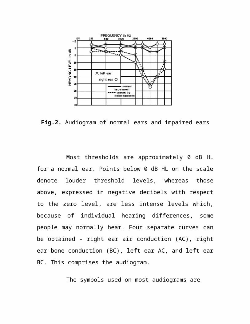
3.3. AUDIOGRAM
An audiogram is a plot of threshold intensity versus frequency.
The intensity scale in HL increases downwards, and hence the audiogram
resembles like an attenuation response, a lower point on the audiogram
indicating higher loss. A typical audiogram (dB HL vs. frequency graph)
comparing normal and impaired hearing is shown in Fig.2. The dip or notch
at 4 kHz as shown, or at 6 kHz, is a symptom of noise-induced hearing loss.
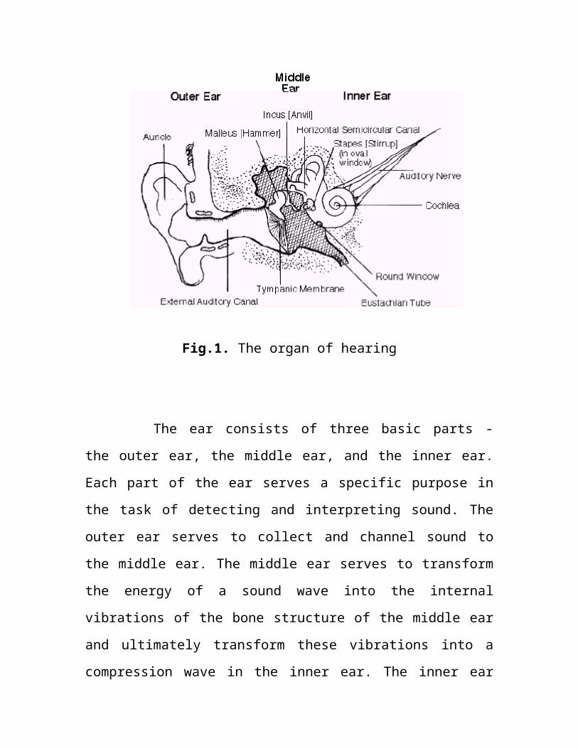
Fig.2. Audiogram of normal ears and impaired ears
Most thresholds are approximately 0 dB HL for a normal ear.
Points below 0 dB HL on the scale denote louder threshold levels, whereas
those above, expressed in negative decibels with respect to the zero level,
are less intense levels which, because of individual hearing differences,
some people may normally hear. Four separate curves can be obtained - right
ear air conduction (AC), right ear bone conduction (BC), left ear AC, and
left ear BC. This comprises the audiogram.
The symbols used on most audiograms are
x - Left air conduction
o - Right air conduction
In normal individuals, a small discrepancy is often seen
between air and bone conduction thresholds, the "AC-BC gap". At any given
frequency the threshold for AC is somewhat lower than BC (i.e., a stronger
signal is needed for BC).
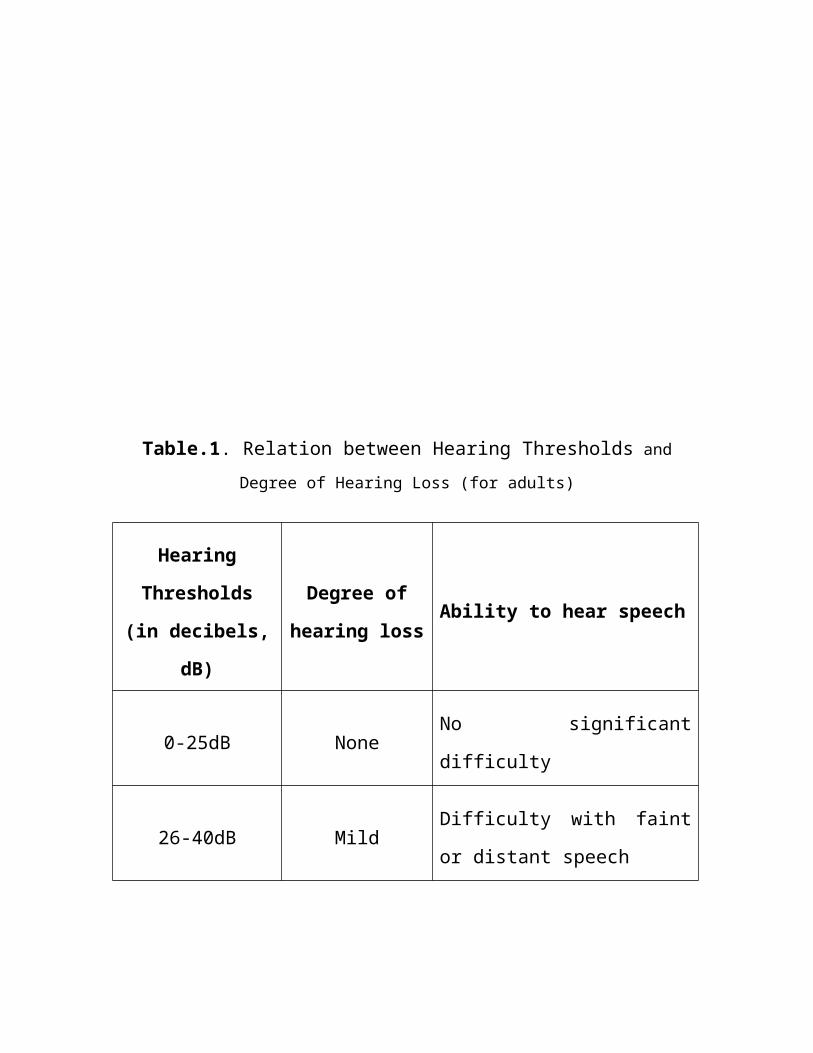
The following table relates hearing thresholds (how loud a
sound of certain frequency must be for a person to hear it) to the degree of
hearing loss for adults.
Table.1. Relation between Hearing Thresholds and Degree of Hearing Loss (for
adults)
Hearing
Thresholds (in
decibels, dB)
Degree of
hearing lossAbility to hear speech
0-25dB None No significant difficulty
26-40dB MildDifficulty with faint or distant
speech
41-55dB ModerateDifficulty with conversational
speech
56-70dBModerate to
severe
Speech must be loud; difficulty
with group conversation
71-90dB Severe
Difficulty with loud speech;
understands only shouted or
amplified speech
91+ dB Profound May not understand amplified
speech
BLOCK DIAGRAM
OF THE AUDIOMETER

4. BLOCK DIAGRAM
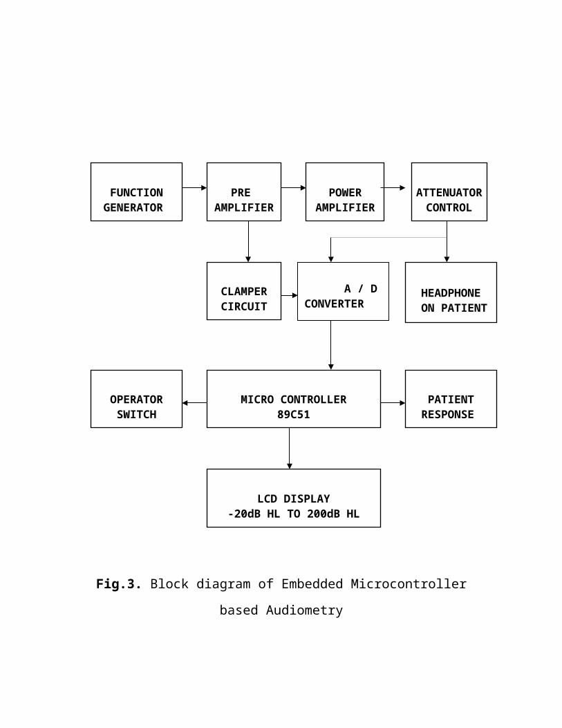
Fig.3. Block diagram of Embedded Microcontroller based Audiometry
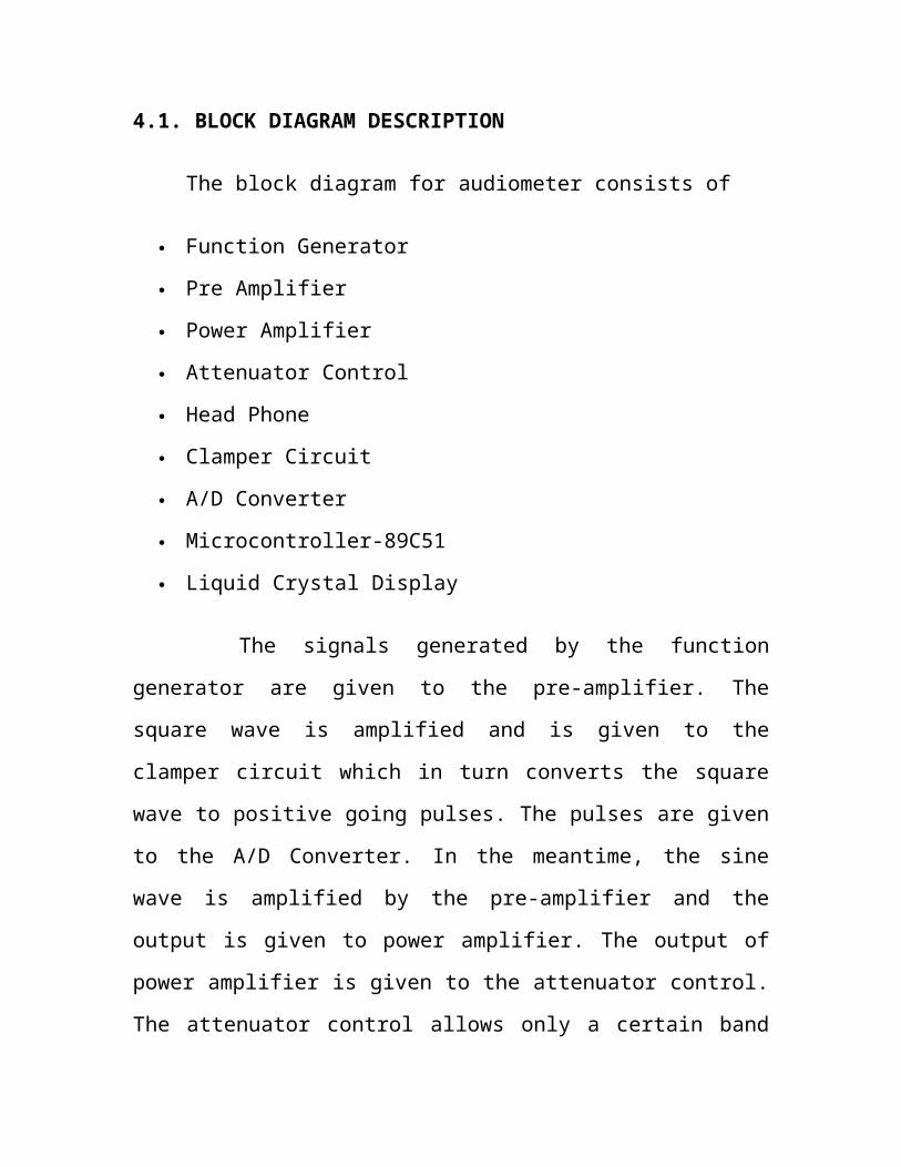
4.1. BLOCK DIAGRAM DESCRIPTION
The block diagram for audiometer consists of
FUNCTIONGENERATOR
PRE AMPLIFIER
POWERAMPLIFIER
ATTENUATORCONTROL
CLAMPERCIRCUIT
HEADPHONE ON PATIENT
PATIENTRESPONSE
LCD DISPLAY-20dB HL TO 200dB HL
MICRO CONTROLLER89C51
OPERATORSWITCH
A / D CONVERTER
Function Generator
Pre Amplifier
Power Amplifier
Attenuator Control
Head Phone
Clamper Circuit
A/D Converter
Microcontroller-89C51
Liquid Crystal Display
The signals generated by the function generator are given to the
pre-amplifier. The square wave is amplified and is given to the clamper
circuit which in turn converts the square wave to positive going pulses. The
pulses are given to the A/D Converter. In the meantime, the sine wave is
amplified by the pre-amplifier and the output is given to power amplifier.
The output of power amplifier is given to the attenuator control. The
attenuator control allows only a certain band of frequencies to the Head
Phone (which should be placed on the patient) and to A/D Converter. The
output of ADC is given to the Microcontroller and finally the output is
displayed with the help of Liquid Crystal Display.
HARDWARE
5. HARDWARE
5.1. POWER SUPPLY
All electronic circuits need dc power supply either from battery
or power back units. It may not be economical and convenient to depend
upon battery power supply. Hence, many electronic equipment contain
circuits which convert the ac supply into dc voltage at the required level.
The unit containing these circuits is called the Linear Mode Power Supply
(LPS). In the absence of ac main supply the dc supply from battery can be
converted into required ac voltage which may be used by computer and
other electronic systems for their operation. Also, in certain applications dc
to dc conversion is required. Such a power supply unit that converts dc into
ac or dc is called Switched Mode Power Supply (SMPS).
1. Linear Mode Power Supply: ac/dc power supply convertor
2. Switched Mode Power Suppy:
a) dc/dc power supply convertor
b) dc/ac power supply convertor
5.1.1. Linear Mode Power Supply
An ac/dc power supply converts ac mains (230V, 50Hz) into
required dc voltages (and is found in all mains operable system). The basic
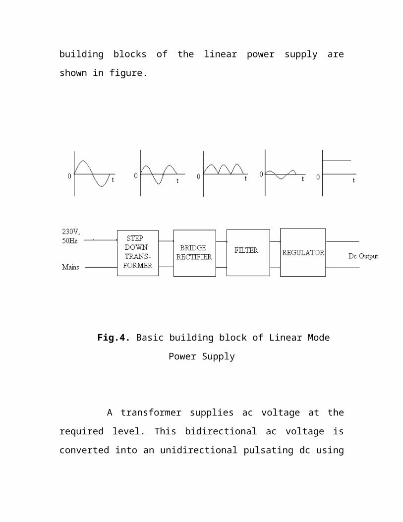
building blocks of the linear power supply are shown in figure.
Fig.4. Basic building block of Linear Mode Power Supply
A transformer supplies ac voltage at the required level. This
bidirectional ac voltage is converted into an unidirectional pulsating dc using
a rectifier. The unwanted ripple contents of this pulsating dc are removed by
a filter to get dc voltage. The output of the filter is fed to a regulator which
gives a steady dc output independent of load variations and input supply
fluctuations.
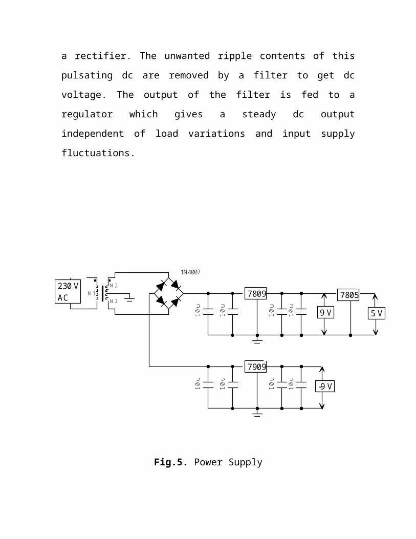
N1N2
N3
1N4007
10
u
10
u
10
u
10
u
10
u
10
u
10
u
10
u
7809 7805
7909
230 VAC
5 V9 V
-9 V
Fig.5. Power Supply
This circuit can give
Table.2. Relation between regulator names and its output voltages
Name Voltage
LM7809 + 9 volts
LM7905 - 5 volts
LM7909 - 9 volts
5.2. FUNCTION GENERATOR
A function generator is an instrument that generates signals for
use in electronic test situations.
A function generator generates signals. We may also find that another
common name for the instrument is signal generator.
The signals produced by a function generator can have many
waveshapes. We may find
o Sinusoidal signals
o Square wave signals
o Triangle signals
o Ramp signals
o Pulses
o Noise signals
o User-defined signals
The frequency of the signals can be controlled.
The amplitude of the signals can be controlled.
Not all of the signals above are found on every function
generator, and there are more specialized functions that can be performed.
In general, a generator that produces the first three signals may be called a
signal generator, and with more functions the generator may be called a
function generator.
There are three basic controls on a function generator. They are:
A control to set frequency.
A control to set wave shape (sinusoid, triangle, square).
A control to set amplitude.
The function generator can be used to do the following adjustments:
To set the frequency to a value by using a pot.
To set the amplitude to a value by using another pot.
To change the wave shape with the help of a rotary switch.
Fig.6. Function Generator
5.2.1. Circuit Description
Built around a single 8038 waveform generator IC, this circuit
produces sine, square or triangle waves from 20Hz to 200 kHz in four
switched ranges. There are both high and low level outputs, which may be
adjusted with the level control.
All of the waveform generation is produced by IC8038. This
versatile IC even has a sweep input, but is not used in this circuit. The IC
contains an internal square wave oscillator, the frequency of which is
controlled by timing capacitors C1 - C4 and the 10k potentiometer. The
tolerance of the capacitors should be 10% or better for stability. The square
wave is differentiated to produce a triangular wave, which in turn is shaped
to produce a sine wave. All this is done internally, with a minimum of
external components. The purity of the sine wave is adjusted by the two
100k preset resistors.
The wave shape switch is a single pole 3 way rotary switch, the
wiper arm selects the wave shape and is connected to a 10k potentiometer,
which controls the amplitude of all waveforms. LM324 op-amp wired as a
standard direct-coupled non-inverting buffer, providing isolation between
the waveform generator, and also increasing output current.
The 2.2k and 47 ohm resistors form the output attenuator. At
the high output, the maximum amplitude is about 8V peak-peak with the
square wave. The maximum for the triangle and sine waves is around 6V
and 4V respectively. The low amplitude controls are useful for testing
amplifiers, as amplitudes of 20mV and 50mV are easily achievable.
5.2.1.1. Setting Up
The two 100k preset resistors adjust the purity of the sine wave.
If adjusted correctly, then the distortion amounts to less than 1%.
5.2.2. IC 8038 Description
The IC8038 waveform generator is a monolithic integrated
circuit capable of producing high accuracy sine, square, triangular, sawtooth
and pulse waveforms with a minimum of external components. The
frequency (or repetition rate) can be selected externally from 0.001Hz to
more than 300 kHz using either resistors or capacitors, and frequency
modulation and sweeping can be accomplished with an external voltage. The
IC8038 is fabricated with advanced monolithic technology, using Schottky
barrier diodes and thin film resistors, and the output is stable over a wide
range of temperature and supply variations. These devices may be interfaced
with phase locked loop circuitry to reduce temperature drift to less than
250ppm/o C.
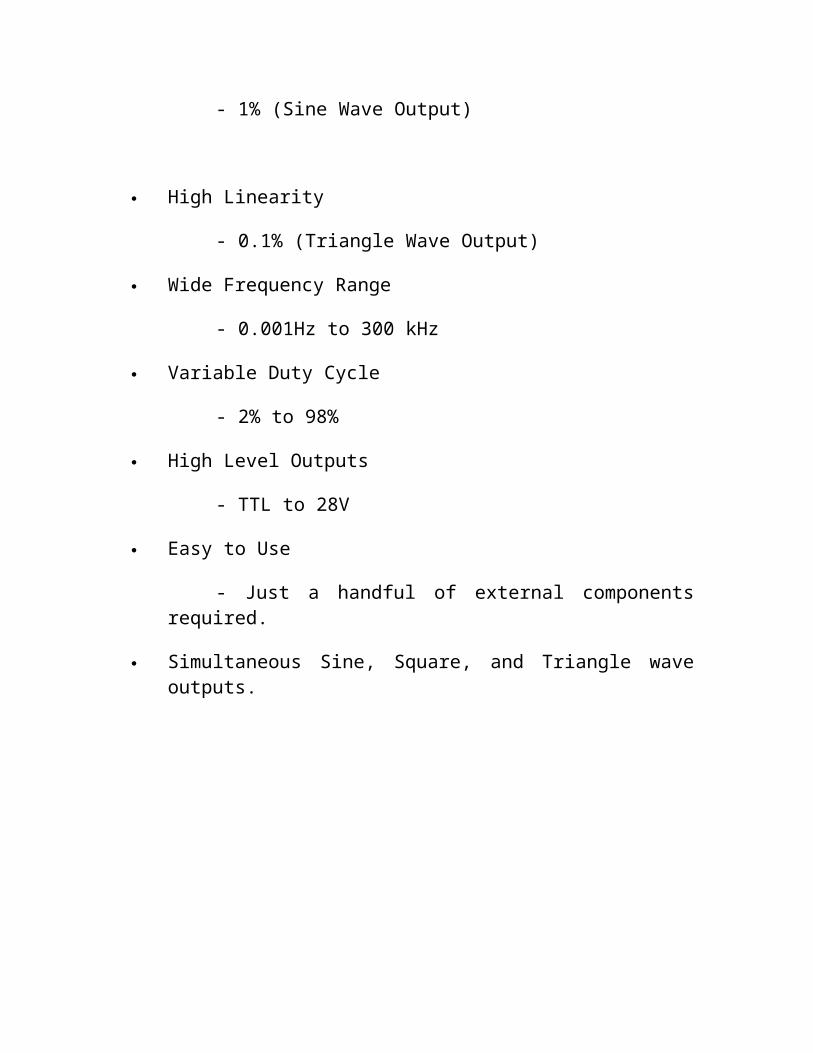
5.2.2.1. Features
Low Frequency Drift with Temperature
- 250ppm/o C
Low Distortion
- 1% (Sine Wave Output)
High Linearity
- 0.1% (Triangle Wave Output)
Wide Frequency Range
- 0.001Hz to 300 kHz
Variable Duty Cycle
- 2% to 98%
High Level Outputs
- TTL to 28V
Easy to Use
- Just a handful of external components required.
Simultaneous Sine, Square, and Triangle wave outputs.
5.3. PRE AMPLIFIER
A two port device which accepts an input signal and produces
an output signal proportional to the input is called as an amplifier. The
proportionality constant between input and output is called as gain of the
amplifier.
An amplifier which amplifies the input without producing any
phase shift between input and output is called non-inverting amplifier. The
input is applied to the non-inverting input terminal of the op-amp. The op-
amp always amplifies the difference input voltage Vd. This difference
voltage is the difference between the voltages Vin and Vf where Vf is the
feedback voltage. The feedback voltage opposes the input voltage that is; it
is 180° out of phase with respect to the input. This indicates that the
feedback is negative.
When the input signal and part of the output signal are in phase,
the feedback is called positive feedback. Use of positive feedback results in
oscillations and hence not used in amplifiers. (Oscillator is an amplifier,
which uses a positive feedback and without any external input signal
generates an output waveform at a desired frequency).
Fig.7. Pre Amplifier
5.3.1. Circuit Description
Two stages are used to avoid oscillations and non-ideal
operation amplifier characteristics when very high gain (10000-1000000
times) configurations. Both amplifier stages are built using an LM324.
The input signal to the preamplifier is in the order of 0.5mV.
The two op-amps of a LM324 integrated circuit chip are employed to
amplify the signals from the function generator. The first amplifier stage
provides a gain of about 20. The second stage, which is identical to the first
stage, provides a subsequent gain of 20 to give a total amplification of about
400.
100k
10u
22k
200n
22
k
100k
10u
22k
200n
22
k
10
n
200n-
+ +
LM324/NS -
+ +
LM324/NS
FromBuffer
To PowerAmplifier
Capacitor C1 is the coupling capacitor for the first amplification
stage and C4 for the second amplification stage. The resistors R1 and R4 are
the compensating resistors and have a value of 22 kW. R2 = Ri = 22kW,
which is the input resistance of first stage and Ri = R5 = 22kW is the input
resistance of the second stage. Capacitors C2 and C5 are of 1 nF value and
are the feedback capacitances of first and second stages respectively. These
capacitances serve to improve the stability of the circuit and the low
frequency response.
5.3.2. IC LM324 Description
The LM324 series consists of four independent, high gain;
internally frequency compensated operational amplifiers which were
designed specifically to operate from a single power supply over a wide
range of voltages. Operation from split power supplies is also possible and
the low power supply current drain is independent of the magnitude of the
power supply voltage.
5.3.2.1. Features
Internally frequency compensated for unity gain
Large DC voltage gain 100 dB
Wide bandwidth (unity gain) 1 MHz (temperature compensated)
Wide power supply range: Single supply 3V to 32V or dual supplies
±1.5V to ±16V
Very low supply current drain (700 µA) - essentially independent of
supply voltage
Low input biasing current 45 nA (temperature compensated)
Low input offset voltage 2 mV and offset current: 5 nA
Input common-mode voltage range includes ground
Differential input voltage range equal to the power supply voltage
Large output voltage swing 0V to V+ -1.5V
5.3.2.2. Unique Characteristics
In the linear mode the input common-mode voltage range includes
ground and the output voltage can also swing to ground, even though
operated from only a single power supply voltage
The unity gain cross frequency is temperature compensated
The input bias current is also temperature compensated
5.3.2.3. Advantages
Eliminates need for dual supplies
Four internally compensated op amps in a single package
Allows directly sensing near GND and VOUT also goes to GND
Compatible with all forms of logic
Power drain suitable for battery operation
5.4. POWER AMPLIFIER
In general, an amplifier receives an input signal from some
transducer or other input source and provides a large amplified signal to
some output device or another amplifier stage. The small signal amplifiers
are basically voltage amplifiers, the voltage and current signal levels are
small in such amplifiers. The output current capability of such amplifier is
limited. The amount of power handling capacity and power efficiency are of
little concern for the small signal amplifiers.
The power amplifier is basically used to amplify an audio
signal faithfully. The loads to such amplifiers are generally loud speakers,
headphones and servomotors. Such loads require large current and sufficient
power, typically few watts to tens of watts. Such power amplifiers develop
and feed the sufficient power to the loads like speakers, motors and
headphones by handling the large signals hence these are also called as large
signal amplifiers or power amplifiers .The low output impedance is another
requirement and such loads which is to be satisfied by the power amplifiers.
Thus the main features of a large signal amplifier or a power amplifier
are,
The large amount of power to be delivered to the load.
The power efficiency.
The impedance matching to the output device.
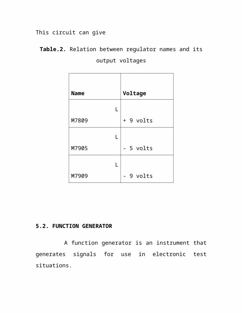
Fig.8. Power Amplifier
5.4.1. Circuit Description
The simplest and most basic application of LM386 is an audio
amplifier. The IC can be used in inverting as well as non-inverting
configuration. When used in the non-inverting mode the inverting terminal
can be either shorted to ground, left open or returned to ground through
resistor or capacitor. Similarly, when it is used in the inverting
configuration, the non-inverting terminal may be either shorted to ground or
returned to ground through resistor or capacitor. In both the configurations,
the supply voltage must be decoupled by connecting a capacitor between the
terminal 6 and ground.
5.4.2. IC LM386 Description
The LM386 is a power amplifier designed for use in low
voltage consumer applications. The gain is internally set to 20 to keep
external part count low, but the addition of an external resistor and capacitor
between pins 1 and 8 will increase the gain to any value from 20 to 200. The
inputs are ground referenced while the output automatically biases to one-
half the supply voltage. The quiescent power drain is only 24 milliwatts
when operating from a 6 volt supply, making the LM386 ideal for battery
operation.
5.4.2.1. Features
Battery operation
Minimum external parts
Wide supply voltage range: 4V–12V or 5V–18V
Low quiescent current drain: 4mA
Voltage gains from 20 to 200
Ground referenced input
Self-centering output quiescent voltage
Low distortion: 0.2% (AV = 20, VS = 6V, RL = 8W, PO =125mW, f
= 1kHz)
Available in 8 pin MSOP package
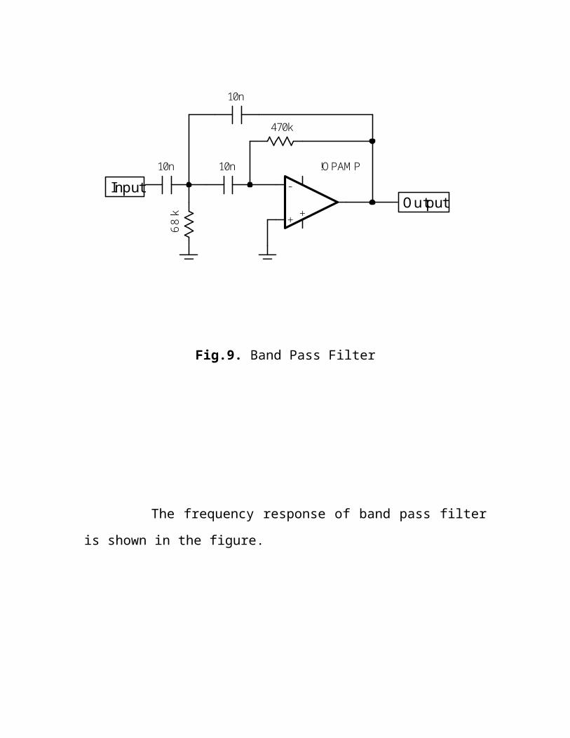
5.5. ATTENUATOR CONTROL
The attenuator control acts as a band pass filter. A band pass
filter is basically a frequency selector. It allows one particular band of
frequencies to pass. Thus, the pass band is between the two cut-off
frequencies fH and fL where fH>fL. Any frequency outside this band gets
attenuated.
-
+ +
!OPAMP
470k
10n 10n
10n
68
k
InputOutput
Fig.9. Band Pass Filter

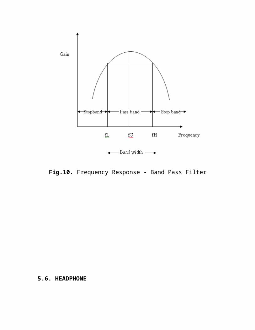
The frequency response of band pass filter is shown in the
figure.
Fig.10. Frequency Response - Band Pass Filter

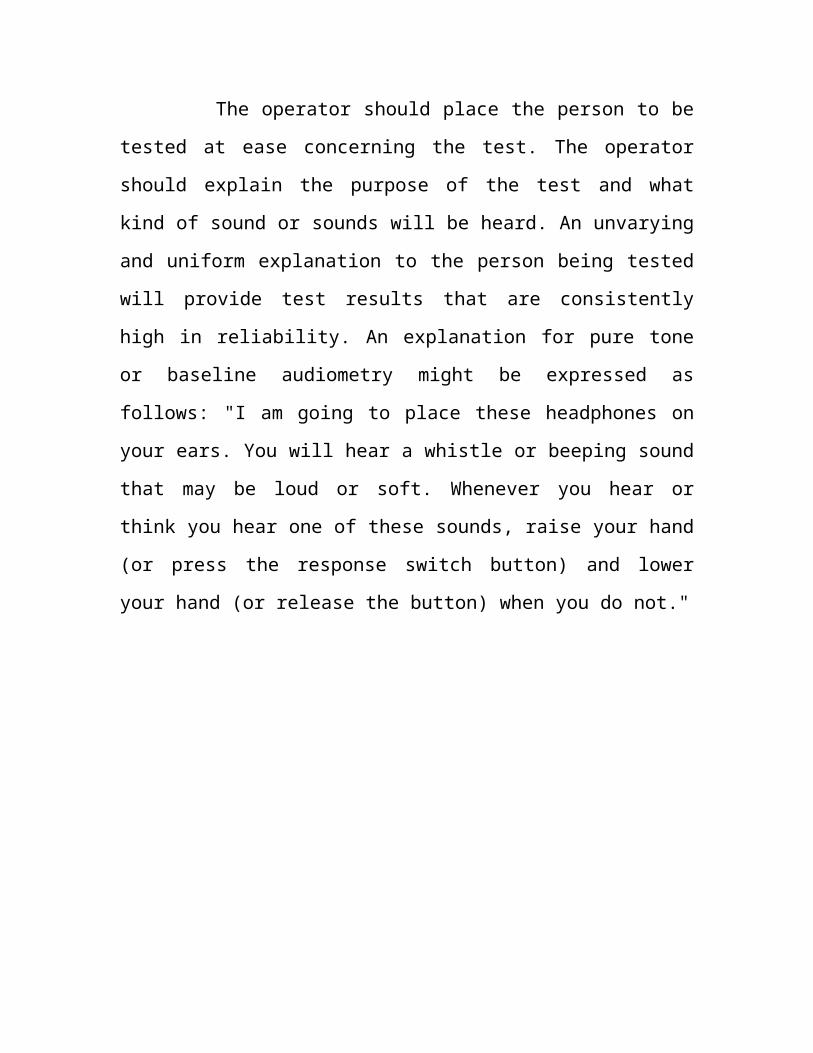
5.6. HEADPHONE
The operator should place the person to be tested at ease
concerning the test. The operator should explain the purpose of the test and
what kind of sound or sounds will be heard. An unvarying and uniform
explanation to the person being tested will provide test results that are
consistently high in reliability. An explanation for pure tone or baseline
audiometry might be expressed as follows: "I am going to place these
headphones on your ears. You will hear a whistle or beeping sound that may
be loud or soft. Whenever you hear or think you hear one of these sounds,
raise your hand (or press the response switch button) and lower your hand
(or release the button) when you do not."
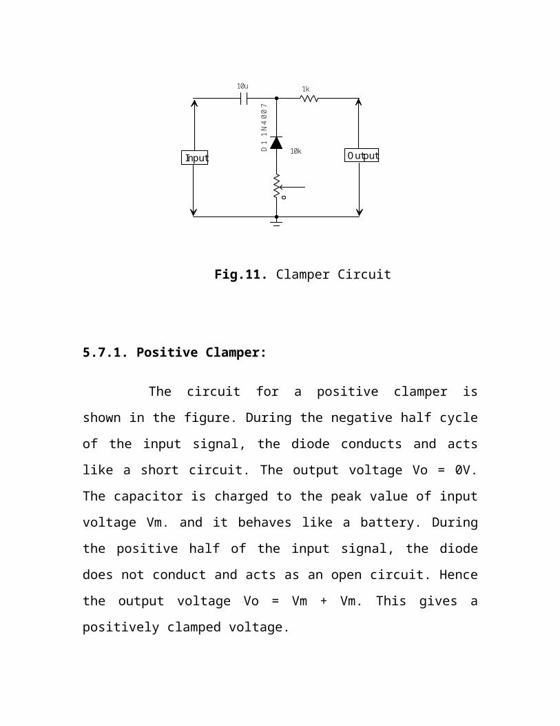
5.7. CLAMPER CIRCUIT
Clamper is a circuit that "clamps" a signal to a different dc
level. The different types of clampers are positive negative and biased
clampers. A clamping network must have a capacitor, a diode and a resistive
element. The magnitude R and C must be chosen such that the time constant
RC is large enough to ensure that the voltage across the capacitor does not
discharge significantly during the interval the diode is non- conducting.
10u 1k
D1
1N
400
7
10kInput Output
Fig.11. Clamper Circuit
5.7.1. Positive Clamper:
The circuit for a positive clamper is shown in the figure. During
the negative half cycle of the input signal, the diode conducts and acts like a
short circuit. The output voltage Vo = 0V. The capacitor is charged to the
peak value of input voltage Vm. and it behaves like a battery. During the
positive half of the input signal, the diode does not conduct and acts as an
open circuit. Hence the output voltage Vo = Vm + Vm. This gives a
positively clamped voltage.
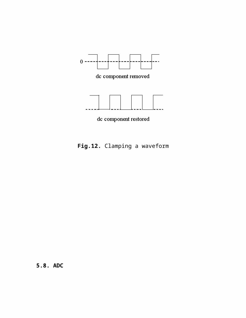
Fig.12. Clamping a waveform
5.8. ADC
Most of the information carrying signals such as voltage,
current, charge, temperature, pressure and time are available in the analog
form. However, for processing, transmission and storage purposes, it is often
more convenient to express such signals in the digital form. When expressed
in the digital form, they provide better accuracy and reduce noise.
Moreover, the development in the microcontroller technology
has made it compulsory to process data in the digital form. Since digital
systems such as microcontroller use a binary system of 1’s and 0’s, we have
to convert signal from analog to digital form. The circuit that performs this
conversion is called an analog to digital (A/D) converter.
Analog to digital converter are classified into two general
groups based on the conversion techniques. One technique involves
comparing a given analog signal with the internally generated reference
voltages. This group includes successive approximation, flash, delta
modulated (DM), adaptive delta modulated and flash type converters.
Another technique involves changing an analog signal into time or
frequency and comparing these new parameters against known values. This
group includes integrator converters and voltage-to-frequency converters.
5.8.1. Successive Approximation ADC
In this technique, the basic idea is to adjust the DAC’s input
code such that its output is within +1/2 LSB of the analog input Vi to be A/D
converted. The code that achieves this represents the desired ADC output.
The successive approximation method uses very efficient code
searching strategy called binary search. It completes searching process for n-
bit conversion in just n clock periods.
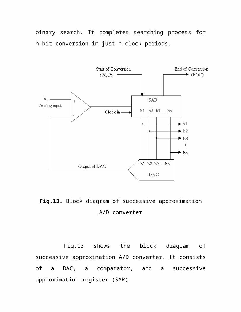
Fig.13. Block diagram of successive approximation A/D converter
Fig.13 shows the block diagram of successive approximation
A/D converter. It consists of a DAC, a comparator, and a successive
approximation register (SAR).
The external clock input sets the internal timing parameters.
The control signal start of conversion (SOC) initiates an A/D conversion
process and end of conversion signal is activated when the conversion is
completed.
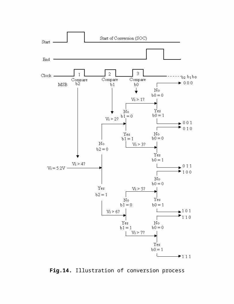
5.8.1.1. Operation
The searching code process in successive approximation
method is similar to weighing an unknown material with a balance scale and
a set of standard weights. Let us assume that we have 1kg, 2kg and 4kg
weights (SAR) plus a balance scale (comparator and DAC). Now we will see
the successive approximation analogy for 3-bit ADC.
Refer Fig.13 and Fig.14. The analog voltage Vin is applied at
one input of comparator. On receiving start of conversion signal (SOC),
successive approximation register sets 3-bit binary code 1002 (b2 = 1) as an
input of DAC. This is similar process of placing the unknown weight on one
platform of the balance and 4kg weight on the other. The DAC converts the
digital word 100 and applies it equivalent analog output at the second input
of the comparator. The comparator then compares two voltages just like
comparing unknown weight with 4kg weight with the help of balance scale.
If the input voltage is greater than the analog output of DAC, successive
approximation register keeps b2 = 1 and makes b1 = 1 (addition of 2kg
weight to have total 6kg weight) otherwise it resets b2 = 0 and makes b1 = 1
(replacing 2kg weight). The same process is repeated for b1 and b0. The
status of b0, b1 and b2 bits gives the digital equivalent of the analog input.
Fig.14 illustrates the process we have just discussed.
The dark line in the Fig.14 shows setting and resetting actions
of bits for input voltage 5.2V, on the basis of compression. It can be seen
from the Fig.14 that one clock pulse is required for the successive
approximation register to compare each bit. However an additional clock
pulse is usually required to reset the register prior to performing a
conversion.
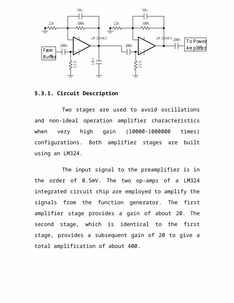
Fig.14. Illustration of conversion process
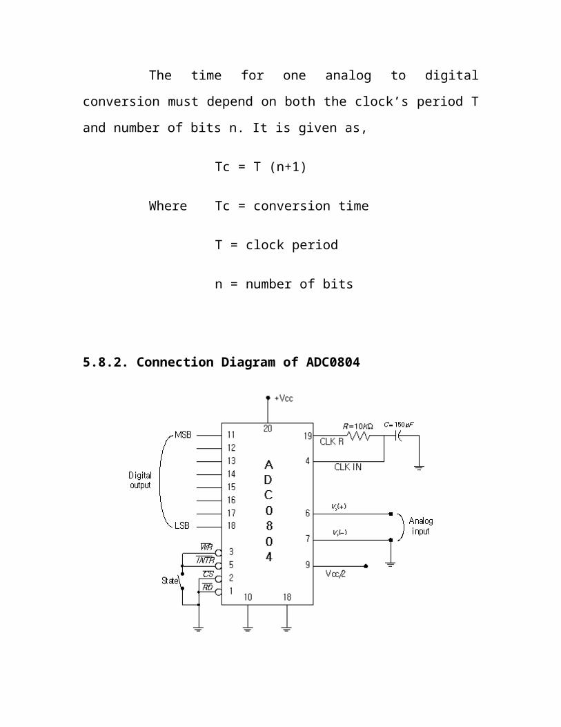
The time for one analog to digital conversion must depend on
both the clock’s period T and number of bits n. It is given as,
Tc = T (n+1)
Where Tc = conversion time
T = clock period
n = number of bits
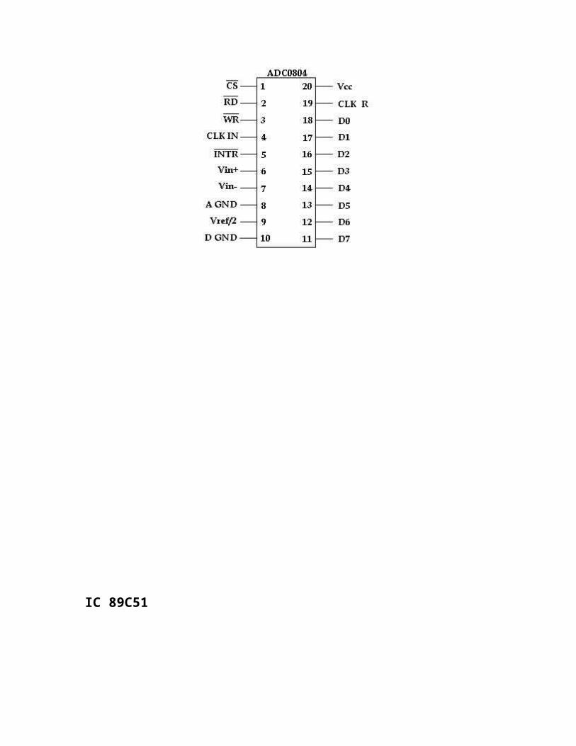
5.8.2. Connection Diagram of ADC0804
Fig.15. Connection Diagram of ADC0804
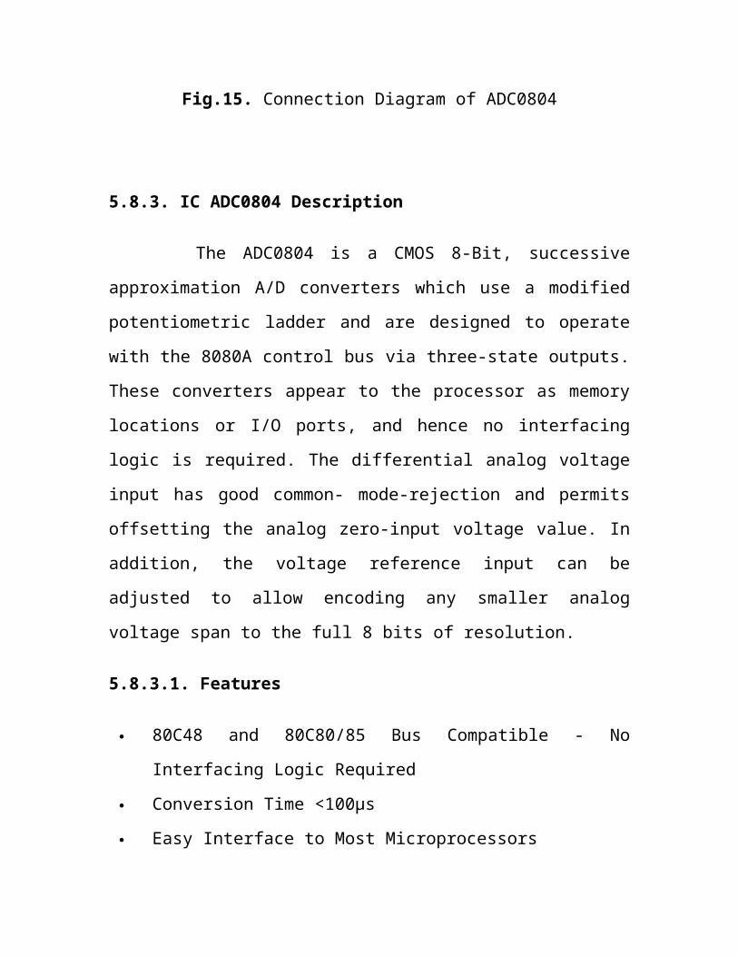
5.8.3. IC ADC0804 Description
The ADC0804 is a CMOS 8-Bit, successive approximation A/D
converters which use a modified potentiometric ladder and are designed to
operate with the 8080A control bus via three-state outputs. These converters
appear to the processor as memory locations or I/O ports, and hence no
interfacing logic is required. The differential analog voltage input has good
common- mode-rejection and permits offsetting the analog zero-input
voltage value. In addition, the voltage reference input can be adjusted to
allow encoding any smaller analog voltage span to the full 8 bits of
resolution.
5.8.3.1. Features
80C48 and 80C80/85 Bus Compatible - No Interfacing Logic
Required
Conversion Time <100µs
Easy Interface to Most Microprocessors
Will Operate in a “Stand Alone” Mode
Differential Analog Voltage Inputs
Works with Band gap Voltage References
TTL Compatible Inputs and Outputs
On-Chip Clock Generator
Analog Voltage Input Range (Single + 5V Supply) 0V to 5V
No Zero-Adjust Required
80C48 and 80C80/85 Bus Compatible - No Interfacing Logic
Required.
SOFTWARE
6. SOFTWARE
6.1. INTRODUCTION TO EMBEDDED SYSTEM
In the literature discussing microprocessors, we often see the
term embedded system. Microprocessors and microcontrollers are widely
used in embedded system products. An embedded product uses a
microprocessor or microcontroller to do one and task only. A printer is an
example of embedded system since the processor inside it performs one task
only ; namely, getting the data and printing it. Contrast this with a Pentium-
based PC (or any x86 IBM-compatible PC). A Pc can be used for any
number of applications such as word processor, print server, bank teller
terminal, video game player, network server, or Internet terminal. Software
for a variety of applications can be loaded and run. Of course the reason a
PC can perform myriad tasks is that it has RAM and an operating system
that loads the application software into RAM and lets the CPU run it. In
embedded system, there is only one application software that is typically
built in ROM.
6.2. IC 89C51 MICROCONTROLLER
The popular 8051 has on-chip ROM in the form of flash
memory. This is ideal for fast development since flash memory can be
erased in seconds compared to twenty minutes or more needed for the 8751.
For this reason the AT89C51 is used in the place of 8751 to eliminate the
waiting time needed to erase the chip and thereby speed up development
time. To use the AT89C51 to develop the microcontroller based system
requires a ROM burner that supports flash memory; however, a ROM eraser
is not needed. Notice that in flash memory we must erase the entire contents
of ROM in order to program it again. This erasing of flash is done by the
PROM burner itself and this why a separate eraser is not needed. To
eliminate the need for a PROM burner we can use AT89C51 that can be
programmed via the serial COM port of an IBM PC.
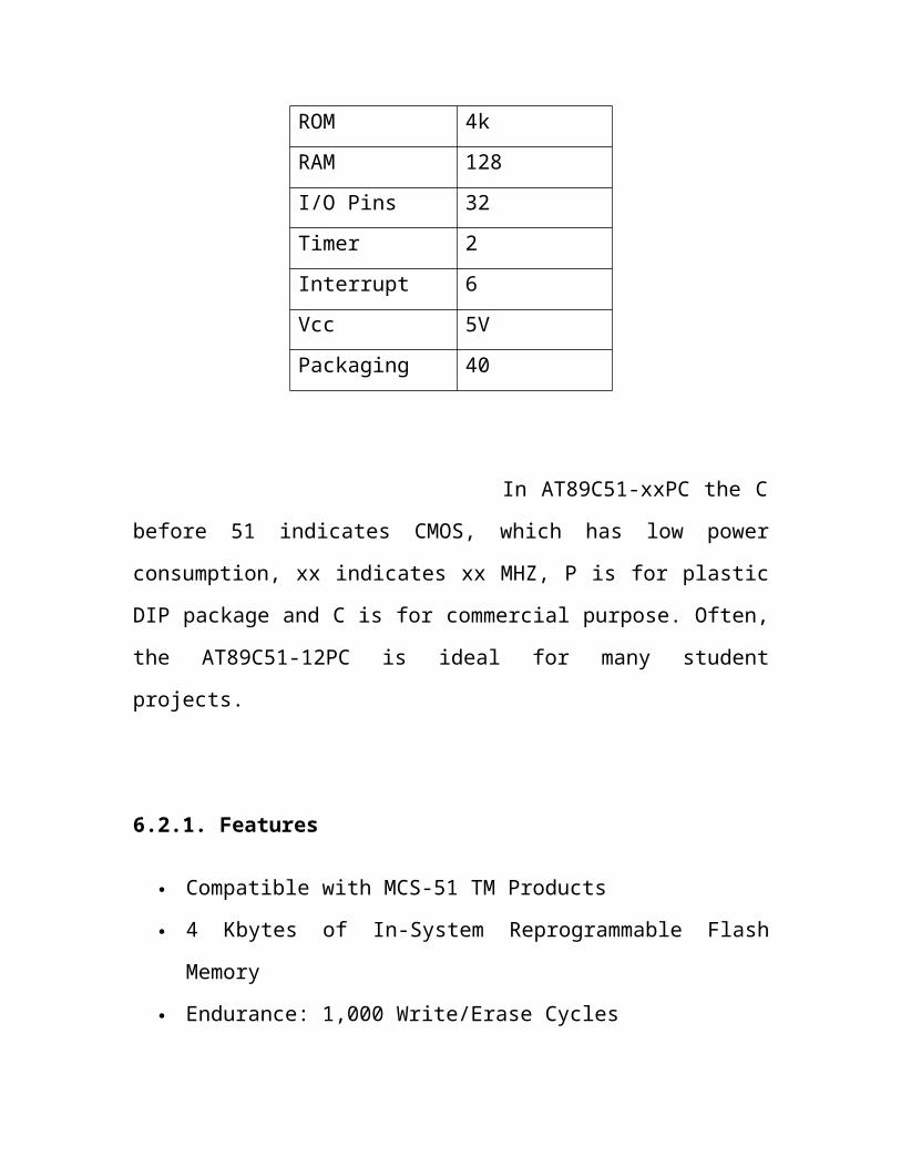
Table.3. Details of IC 89C51
ROM 4k
RAM 128
I/O Pins 32
Timer 2
Interrupt 6
Vcc 5V
Packaging 40
In AT89C51-xxPC the C before 51 indicates CMOS, which
has low power consumption, xx indicates xx MHZ, P is for plastic DIP
package and C is for commercial purpose. Often, the AT89C51-12PC is
ideal for many student projects.
6.2.1. Features
Compatible with MCS-51 TM Products
4 Kbytes of In-System Reprogrammable Flash Memory
Endurance: 1,000 Write/Erase Cycles
Fully Static Operation: 0 Hz to 24 MHz
Three-Level Program Memory Lock
128 x 8-Bit Internal RAM
32 Programmable I/O Lines
Two 16-Bit Timer/Counters
Six Interrupt Sources
Programmable Serial Channel
Low Power Idle and Power Down Modes
6.2.2. Description
The AT89C51 is a low-power, high-performance CMOS 8-bit
Microcomputer with 4 Kbytes of Flash Programmable and Erasable Read
Only Memory (PEROM). The device is manufactured using Atmel’s high
density nonvolatile memory technology and is compatible with the industry
standard MCS-51TM instruction set and pinout. The on-chip Flash allows
the program memory to be reprogrammed in-system or by a conventional
nonvolatile memory programmer. By combining a versatile 8-bit CPU with
Flash on a monolithic chip, the Atmel AT89C51 is a powerful
microcomputer which provides a highly flexible and cost effective solution
to many embedded control applications.
The AT89C51 provides the following standard features: 4
Kbytes of Flash, 128 bytes of RAM, 32 I/O lines, two 16-bit timer/counters,
five vector two-level interrupt architecture, a full duplex serial port, on-chip
oscillator and clock circuitry. In addition, the AT89C51 is designed with
static logic for operation down to zero frequency and supports two software
selectable power saving modes
LIQUID CRYSTAL DISPLAY
7. LIQUID CRYSTAL DISPLAY
The supper twist back-lit Liquid Crystal Display (LCD) serves
as a visual communication link between the audiometer and its operator.
LCD’s do not generate light but they scatter light. LCD’s
consume very less power and they have good contrast ratio.
It is also called an electroluminescent display. The LCD
consists of a thin layer of normally transparent LC material between two
electrodes. When an electric field is applied, the material becomes turbulent,
reflecting and scattering ambient light. It provides excellent brightness under
high ambient light conditions and requires only 50W of power per
segment. This power is much lower as compared to that for the LED. But the
life expectancy is not as high as that of the LED. The required crystal
displays are used in watches, pocket calculators, pocket televisions and
portable instrument displays.
CONCLUSION
8. CONCLUSION
Thus the Embedded Microcontroller Based Audiometer is used
to determine the sensitivity of the human ear. Accurate assessment of the
hearing loss can be done using this device.
The conventional audiometer is analog in nature. In this project
the embedded micro-controller concepts are implemented to make
audiometry more versatile, cost effective and simpler in design.
In future, we can enhance the system by having additional
graphic features, data storage and signal processing advantage of a PC based
system, with the added benefit of economy and portability.
APPENDICIES
9. APPENDICIES
9.1 APPENDIX 1
SPECIFICATIONS
GENERAL
Power - 230v AC
Display - LCD; 16 characters x 2 lines
Presentation - Pure tone
Repetition Rate - Pseudo-random intervals
Standard Accessories - TDH-39 headset, patient response
button, user's guide
Optional Accessories - Carrying case, noise excluding
headphone enclosures, sound
room cords
AUDIOMETER
Frequencies - 250*, 1K*, 500, 1K, 2K, 3K, 4K, 6K,
8K Hz
Hearing Levels - 0-90 dB HL except 250 & 8K Hz to
70 dB HL
9.2 APPENDIX 2
IC DETAILS
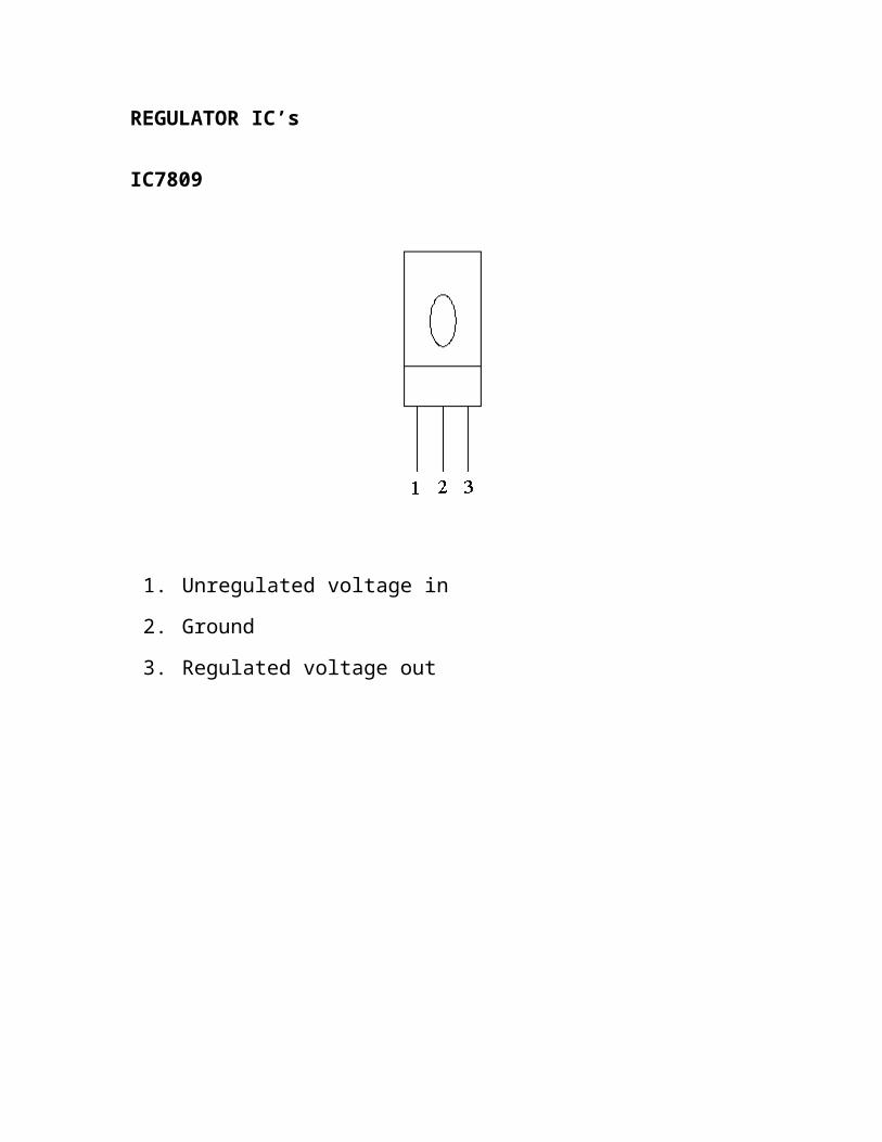
REGULATOR IC’s
IC7809
1. Unregulated voltage in
2. Ground
3. Regulated voltage out
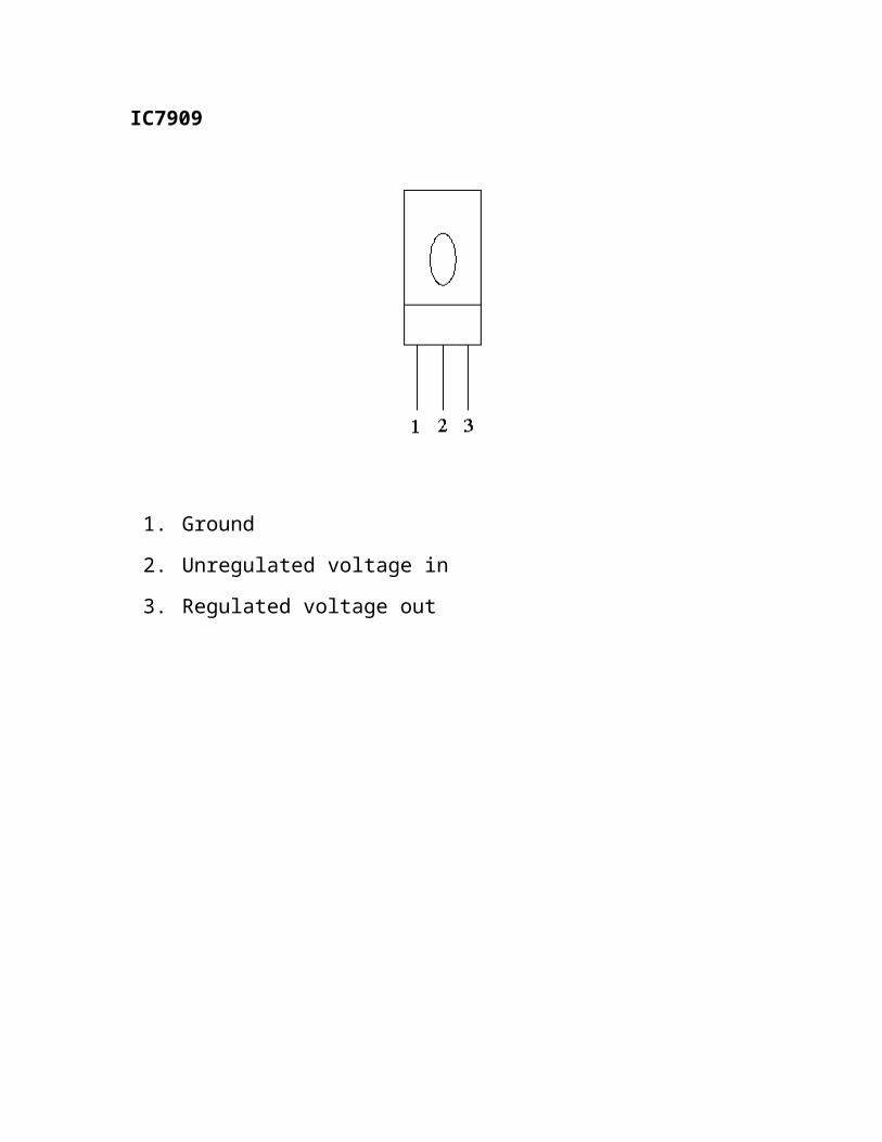
IC7909
1. Ground
2. Unregulated voltage in
3. Regulated voltage out
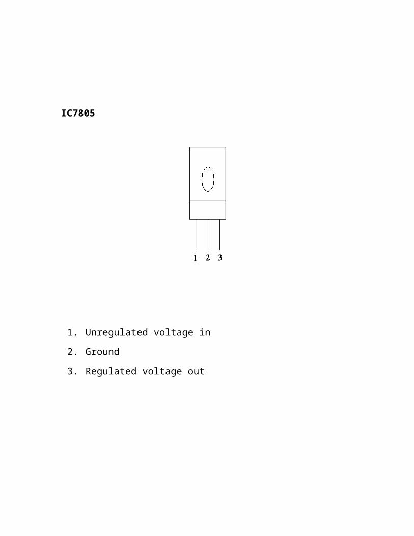
IC7805
1. Unregulated voltage in
2. Ground
3. Regulated voltage out
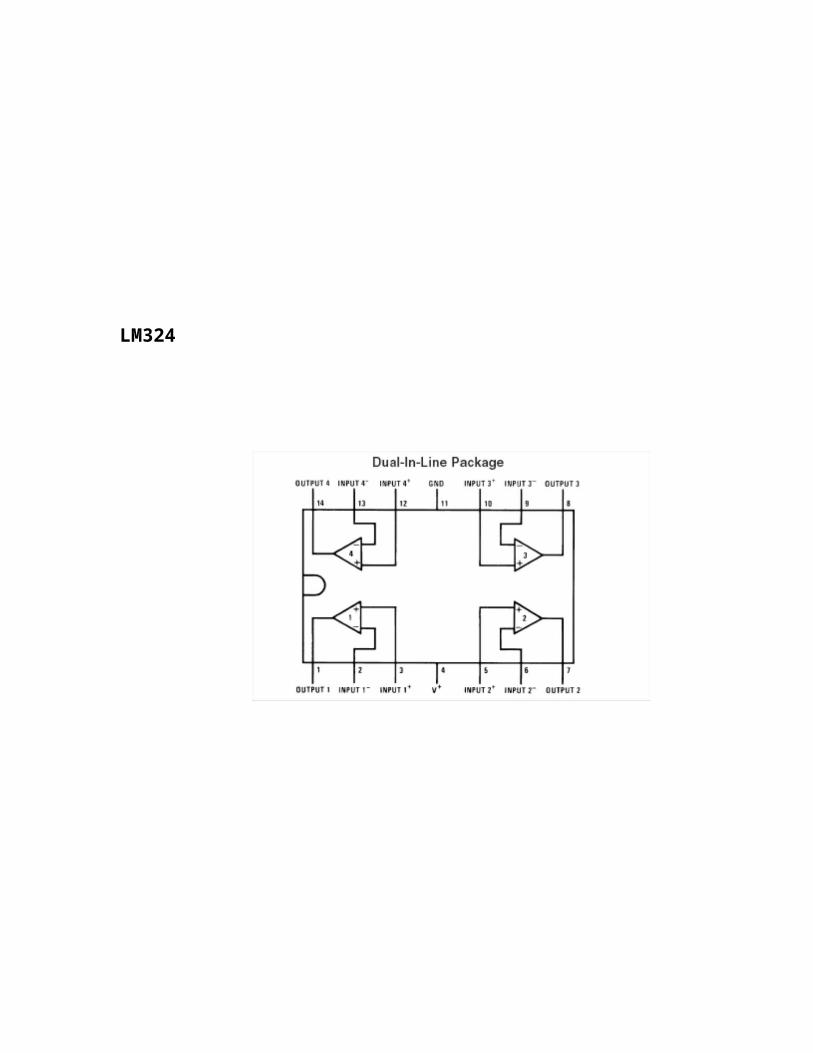
LM324
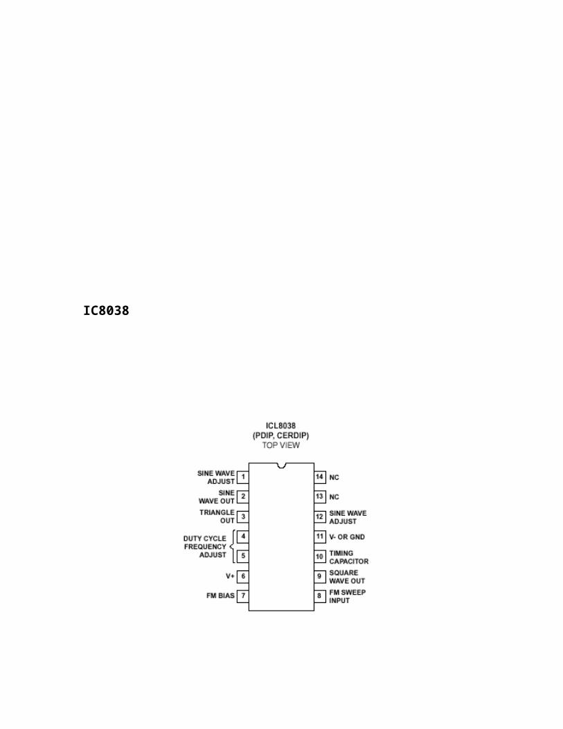
IC8038
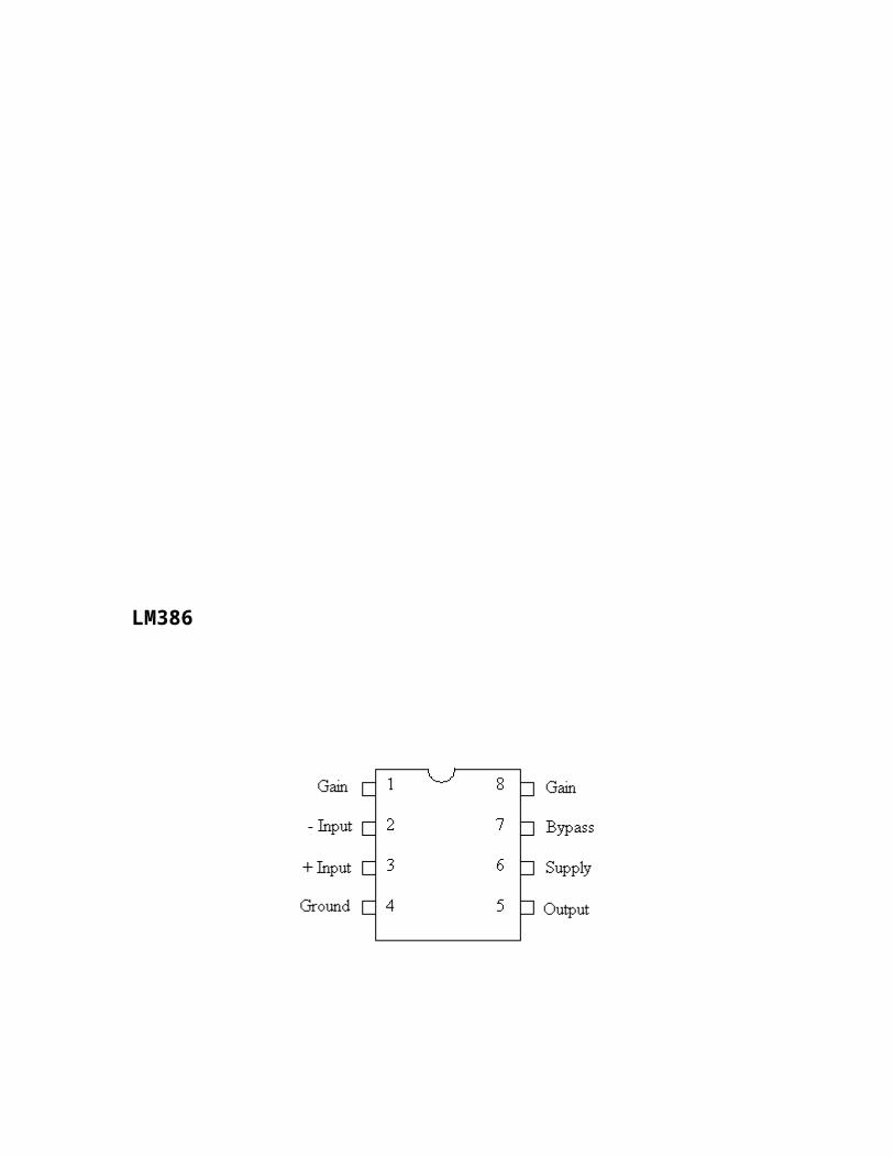
LM386

ADC0804
IC 89C51
9.3 APPENDIX 3
CODING
ORG 0H
CLR A
MOV 80H,A ;Clear port 0
MOV 90H,A ;Clear port 1
MOV 0A0H,A ;clr p2
MOV 0B0H,A;clr p3
MOV R0,A
CL: CLR A
MOV @R0,A
INC R0
CJNE R0,#7EH,CL
CLR 94H
MOV 1FH,#2AH
MOV A,#3CH;
ACALL COM
MOV A,#0EH;curser blink command
ACALL COM
MOV A,#06H;curser on
ACALL COM
MOV A,#1
ACALL COM
ACALL DE
ACALL DE
MOV DPTR,#330H
ACALL BARATI
ACALL DEE
ACALL DEE
ACALL DEE
ACALL DEE
MOV A,#1
ACALL COM
ACALL DEE
ACALL DEE
MOV DPTR,#340H
ACALL BARATI
ACALL DEE
ACALL DEE
ACALL DEE
ACALL DEE
MOV A,#1
ACALL COM
ACALL DEE
ACALL DEE
MOV DPTR,#350H
ACALL BARATI
ACALL DEE
ACALL DEE
ACALL DEE
ACALL DEE
MOV A,#1
ACALL COM
ACALL DEE
ACALL DEE
MOV DPTR,#360H
ACALL BARATI
ACALL DEE
ACALL DEE
ACALL DEE
ACALL DEE
MOV A,#1
ACALL COM
ACALL DEE
ACALL DEE
MOV DPTR,#370H
ACALL BARATI
ACALL DEE
ACALL DEE
ACALL DEE
ACALL DEE
MOV A,#1
ACALL COM
ACALL DEE
ACALL DEE
MOV DPTR,#380H
ACALL BARATI
ACALL DEE
ACALL DEE
ACALL DEE
ACALL DEE
MOV A,#1
ACALL COM
ACALL DEE
ACALL DEE
MOV DPTR,#390H
ACALL BARATI
ACALL DEE
ACALL DEE
ACALL DEE
ACALL DEE
MOV A,#1
ACALL COM
ACALL DEE
ACALL DEE
MOV DPTR,#300H
ACALL BARATI
MOV DPTR,#310H
ACALL RANI
SENI:CLR A
CLR 95H
MOV 1AH,#28H
MOV 1BH,#50H
MOV 89H,#10H;TMOD
MOV 8BH,A
MOV 8DH,A
MOV 22H,#40H
MOV 23H,#42H
MOV 24H,#0FH
MOV 1DH,A
BB: JNB 90H,DD4
ACALL DEE
ACALL DEE
AJMP D4
DD4: JNB 93H,BBB
ACALL ARU
BBB: JB 94H,BB
CLR A
MOV R4,A
MOV R5,A
MOV R6,A
MOV R7,A
L1: JNB 94H,L1
SETB 8EH;TR1
L2: JB 94H,L2
KK: JNB 94H,KK
CLR 8EH;TR1
MOV 1AH,8BH;TL1
MOV 1BH,8DH;TH1
MOV 20H,1BH
;MOV A,1AH
;ADDC A,1AH
;JNC L3
;INC 1BH
;L3:MOV 1AH,A
MOV A,20H
;ADDC A,1BH
;JNC L4
;INC 21H
L4: MOV 1BH,A
L5: MOV A,22H
SUBB A,1AH
INC A
MOV 22H,A
MOV A,23H
SUBB A,1BH
MOV 23H,A
MOV A,24H
SUBB A,21H
MOV 24H,A
JNC LL5
SJMP SENI1
LL5: INC R4
CJNE R4,#10,L5
INC R5
MOV R4,#0
CJNE R5,#10,L5
INC R6
MOV R5,#0
CJNE R6,#10,L5
INC R7
MOV R6,#0
CJNE R7,#10,L5
INC 1DH
MOV R7,#0
SJMP L5
SENI1:ACALL DISPLAY
D12: ;CJNE R5,#0,XX
;CJNE R6,#0,XX
;SJMP XX1
;XX: ACALL DEE
XX1: CLR 97H ;interrupts to adc
ACALL DEE
SETB 97H
MOV A,0A0H
;CPL A
MOV 19H,A
ACALL CAL
;MOV DPTR,#200H
;MOVC A,@A+DPTR
ACALL CAA
;MOV 19H,A
;ACALL CA ;split the full number to display
;ACALL D
ACALL DISPLAY1
; MOV A,12H ;threshold which is in 12h moved to accumulator
; SUBB A,R4 ;port value is available in r4 subtracted with acc
; JNC G4
; SETB 96H ;buzzer & led
;G4: ACALL DEE
; ACALL DEE
; CLR 96H
; JNB 95H,G5; peakhold switch
;SE2: ACALL DEE
; JNB 93H,SE1 ;saving switch
; ACALL DEE
; ACALL DEE
; SJMP SE3
;SE1: JB 95H,SE2
; ACALL DEE
; ACALL DEE
; SJMP D12
;SE3: MOV R0,1AH
; MOV @R0,19H
; INC 1AH
; MOV R0,1BH
; MOV A,R7
; MOV 0F0H,R6

; MUL AB
; MOV @R0,A
; INC 1BH
; INC R0
; MOV A,R5
; MOV 0F0H,R4
; MUL AB
; MOV @R0,A
;INC 1AH
; CLR 0B4H
; CLR 0B0H
; ACALL DEE
; ACALL DEE
; SETB 0B4H
; SETB 0B0H
; MOV 1AH,R0
; SJMP SE2
RE: AJMP SENI
;HH:JNB 90H,HH
D4: ;MOV 1EH,#2AH
;CLR 0B1H;SECOND MODE INDICATION
;SETB 0B2H
MOV DPTR,#320H
ACALL BARATI
MOV R0,#2AH
MOV A,@R0
MOV 1DH,A
INC R0
MOV A,@R0
MOV R7,A
INC R0
MOV A,@R0
MOV R6,A
INC R0
MOV A,@R0
MOV R5,A
INC R0
MOV A,@R0
MOV R4,A
ACALL DISPLAY
INC R0
MOV 28H,R0
MOV A,@R0
ACALL CAL
ACALL DISPLAY1
G6: JNB 91H,G7
MOV R0,28H
INC R0
MOV A,@R0
MOV 1DH,A
INC R0
MOV A,@R0
MOV R7,A
INC R0
MOV A,@R0
MOV R6,A
INC R0
MOV A,@R0
MOV R5,A
INC R0
MOV A,@R0
MOV R4,A
ACALL DISPLAY
INC R0
MOV 28H,R0
MOV A,@R0
ACALL CAL
ACALL DISPLAY1
MOV R0,28H
ACALL DEE
ACALL DEE

G7: JNB 92H,G8
MOV R0,28H
DEC R0
MOV A,@R0
MOV 1DH,A
DEC R0
MOV A,@R0
MOV R7,A
DEC R0
MOV A,@R0
MOV R6,A
DEC R0
MOV A,@R0
MOV R5,A
DEC R0
MOV A,@R0
MOV R4,A
ACALL DISPLAY
DEC R0
MOV 28H,R0
MOV A,@R0
ACALL CAL
ACALL DISPLAY1
ACALL DEE
ACALL DEE
MOV R0,28H
G8: JNB 90H,G6
ACALL DEE
ACALL DEE
MOV R0,#0
MOV DPTR,#300H
ACALL BARATI
AJMP SENI
ARU: MOV R0,1FH;#2AH
MOV @R0,1DH
INC R0
INC 1FH
MOV @R0,07H
INC R0
INC 1FH
MOV @R0,06H
INC R0
INC 1FH
MOV @R0,05H
INC R0
INC 1FH
MOV @R0,04H
INC R0

INC 1FH
MOV @R0,19H
INC R0
INC 1FH
SETB 95H
ACALL DEE
ACALL DEE
ACALL DEE
CLR 95H
RET
BARATI:MOV A,#80H
ACALL COM
B1: CLR A
MOVC A,@A+DPTR
CJNE A,#2DH,C1
RET
C1: ACALL DAT
INC DPTR
SJMP B1
F2: MOV 15H,#240
RANI: MOV A,#0C0H
ACALL COM
BB1: CLR A
MOVC A,@A+DPTR
CJNE A,#2DH,CB1
RET
CB1: ACALL DAT
INC DPTR
SJMP BB1
CAL: MOV 1CH,#0
MOV R1,#0
MOV R2,#0
MOV R3,#0
CJNE A,#0,GF1
SJMP DC
GF1: INC 1CH
INC R1
INC R1
CJNE R1,#10,GF
INC R2
MOV R1,#0
CJNE R2,#10,GF
INC R3
MOV R2,#0
GF: MOV R0,1CH
CJNE A,1CH,GF1
DC: RET
CAA: MOV A,R3
MOV 0F0H,#100
MUL AB
MOV 1EH,A
MOV A,R2
MOV 0F0H,#10
MUL AB
ADDC A,R1
ADDC A,1EH
RET
ADDD:MOV 0F0H,#100
DIV AB
MOV R3,A
MOV A,0F0H
MOV 0F0H,#10
DIV AB
MOV R2,A
MOV R1,0F0H
RET
DISPLAY:MOV A,#8AH
ACALL COM
MOV A,1DH
ADD A,#30H
ACALL DAT
MOV A,R7
ADD A,#30H
ACALL DAT
MOV A,R6
ADD A,#30H
ACALL DAT
MOV A,R5
ADD A,#30H
ACALL DAT
MOV A,R4
ADD A,#30H
ACALL DAT
RET
DISPLAY1: MOV A,#0C6H
ACALL COM
MOV A,R3
ADD A,#30H
ACALL DAT
MOV A,R2
ADD A,#30H
ACALL DAT
MOV A,R1
ADD A,#30H
ACALL DAT
;MOV A,R4
;ADD A,#30H
;ACALL DAT
RET
DAT: MOV 80H,A
SETB 0B7H
CLR 0B5H
SETB 0B6H
CLR 0B6H
ACALL DE
RET
COM:MOV 80H,A
CLR 0B7H
CLR 0B5H
SETB 0B6H
CLR 0B6H
ACALL DE
RET
DE: MOV 17H,#250
KK1: DJNZ 17H,KK1
RET
DEE: MOV 18H,#250
GG1: ACALL DE
ACALL DE
DJNZ 18H,GG1
RET
ORG 300H
DB "FREQUENCY: -"
ORG 310H
DB "POWER: -"
ORG 320H
DB "SAVED FRE: -"
ORG 330H
DB " EMBEDDED -"
ORG 340H
DB " AUDIOMETRY -"
ORG 350H
DB " DONE BY -"
ORG 360H
DB "D.AMBUJAM -"
ORG 370H
DB " V.RANJINI -"
ORG 380H
DB " K.MUTHARASI -"
ORG 390H
DB " S.LAKSHMI -"
END
Instruction Set
Alphabetical List of Instructions
ACALL: Absolute Call
ADD, ADDC: Add Accumulator (With Carry)
AJMP: Absolute Jump
ANL: Bitwise AND
CJNE: Compare and Jump if Not Equal
CLR: Clear Register
CPL: Complement Register
DA: Decimal Adjust
DEC: Decrement Register
DIV: Divide Accumulator by B
DJNZ: Decrement Register and Jump if Not Zero
INC: Increment Register
JB: Jump if Bit Set
JBC: Jump if Bit Set and Clear Bit
JC: Jump if Carry Set
JMP: Jump to Address
JNB: Jump if Bit Not Set
JNC: Jump if Carry Not Set
JNZ: Jump if Accumulator Not Zero
JZ: Jump if Accumulator Zero
LCALL: Long Call
LJMP: Long Jump
MOV: Move Memory
MOVC: Move Code Memory
MOVX: Move Extended Memory
MUL: Multiply Accumulator by B
NOP: No Operation
ORL: Bitwise OR
POP: Pop Value From Stack
PUSH: Push Value Onto Stack
RET: Return From Subroutine
RETI: Return From Interrupt
RL: Rotate Accumulator Left
RLC: Rotate Accumulator Left Through Carry
RR: Rotate Accumulator Right
RRC: Rotate Accumulator Right Through Carry
SETB: Set Bit
SJMP: Short Jump
SUBB: Subtract From Accumulator With Borrow
SWAP: Swap Accumulator Nibbles
XCH: Exchange Bytes
XCHD: Exchange Digits
XRL: Bitwise Exclusive OR
Undefined: Undefined Instruction
REFERENCES

9. REFERENCES
Books
1. G.K. Mithal and Ravi Mittal (2000) ‘Electronic Devices and Circuits’, pp. 726, 758.
2. Muhammad Ali Mazadi and Janice Gillispie Mazadi (2002) ‘The 8051 Microcontroller and Embedded System’
3. D.Roy Choudhury and Shail B. Jain (2004) ‘Linear Integrated Circuits’, pp. 44-93, 380-402
Websites
1. www.electronics-lab.com2. www.earinfo.com
3. www.ee.mut.ac.th/datasheet /
4. www.circuitcellar.com