electronic excitations in topological insulators abstract topological insulators with conducting...
TRANSCRIPT

Electronic excitations in Topological Insulators
studied by Electron Energy Loss Spectroscopy
by
Ganesh Subramanian
A Thesis Presented in Partial Fulfillment of the Requirements for the Degree
Master of Science
Approved October 2013 by the Graduate Supervisory Committee:
John. C. H. Spence, Chair
Allen Nan Jiang Tingyong Chen Candace Chan
ARIZONA STATE UNIVERSITY
December 2013

i
ABSTRACT
Topological insulators with conducting surface states yet insulating bulk states
have generated a lot of interest amongst the physics community due to their varied
characteristics and possible applications. Doped topological insulators have presented
newer physical states of matter where topological order co-exists with other physical
properties (like magnetic order). The electronic states of these materials are very
intriguing and pose the problems and the possible solutions to understanding their unique
behaviors.
In this work, we use Electron Energy Loss Spectroscopy (EELS) – an analytical
TEM tool to study both core-level and valence-level excitations in Bi2Se3 and
Cu(doped)Bi2Se3 topological insulators. We use this technique to retrieve information on
the valence, bonding nature, co-ordination and lattice site occupancy of the undoped and
the doped systems. Using the reference materials Cu(I)Se and Cu(II)Se we try to compare
and understand the nature of doping that copper assumes in the lattice. And lastly we
utilize the state of the art monochromated Nion UltraSTEM 100 to study
electronic/vibrational excitations at a record energy resolution from sub-nm regions in the
sample.

ii
ACKNOWLEDGMENTS
It has been a great 2.5 years at Dr. John Spence’s group. My first thanks are due
to Dr. Amish Shah. Within the 1 month that we had together, he got me into the work and
group ethics and stood through probably the most stupid portions of my alter ego. Most
importantly, he ramped me into TEM and definitely deserves a sincere and friendly
acknowledgement.
Dr. Nan Jiang has been a very close part of our research right from the start. John
holds him in very high regard and it has always been fun interacting with Dr. Nan Jiang
regarding core-loss EELS and FEFF. Saturdays could be interesting as well … and the
few times I had met him on a Saturday, I got to know his kid J We probably have a
longer journey to ride together and so I will reserve my complete appreciation of all his
support for a little later!
Shibom Basu – the nature man :D … partner at crime [except the whole world
would know that he is upto something even before he makes up his mind … lightning fast
is he ;)]. The best compliment he ever received for his TA – ‘He has a great dressing
sense’. Im disappointed every time he comes back alone from California … If I were to
ever trust myself to an investment banker, it would have to be him :D
Nadia – easily the most neat and well-dressed physicist I have come across! I
think Shibom and I together give her a hard fight to keep the average presentation sense
for our group as low as possible :D Music is always an interesting subject to discuss …
need to find the right occasions to do more with her … And ohh, she is a big fan of
Bikram yoga – a yoga mat and tons of sweat is all one needs to get her best wishes J.

iii
Dingjie and Dan are my sole compatriots. With all the action happening in the
neighboring room, they give me a feel of relief to know im not the only person sitting
alone in a window-less room!
Yuin … I have to be careful talking to him because sometimes when I joke I don’t
know if he takes it as an offense J On a totally unrelated note, I will get demoralized if I
sit next to him for 5 minutes … I can never study as much as him.
Chufeng Li – and his gang of friends :D … Chufeng reminds me exactly of what I
would have caricatured as a Chinese monk. I hope I did good enough to give him a
decent opinion of the group and work ethic. A lot to share with him and about him … a
bigger acknowledgement is in store for him, just a little later!
Toshi is the ‘in’ man … If one had to assess popularity votes, he would be the
most sought after person in the TEM area in ASU (leaving out administration). A lot to
learn from him and his experience … im really looking forward to the onward journey J
And finally John - easily the most fun person I have met so far. Lots of energy
and a very practical lifestyle is almost characteristic of him. Asking for opinion is the best
part of interaction with John … when he is in mood he is very witty and it can make your
day. Lots and lots to learn … Lots to observe from close and far. I owe the biggest thanks
to him and hope to be inspired for many more years to come.

iv
TABLE OF CONTENTS
Page
LIST OF ABBREVIATIONS…………………………………………………………….vi
LIST OF FIGURES………………………………………………………………….….viii
CHAPTER
1 INTRODUCTION………………………………………………………...1
1.1 Electron Energy Loss Spectroscopy…………………………………..1
1.2 NION………………………………………………………………….4
1.3 Topological Insulators………………………………………………...6
1.4 Bismuth Selenide…………………………………………………….12
2 EXPERIMENTS…………………………………………………………15
2.1 Samples Instruments and Softwares…………………………………15
2.2 TEM sample preparation…………………………………………….16
2.3 2010F and Core-Loss………………………………………………...18
2.3.1 Preliminary TEM…………………………………………..18
2.3.2 Core-Loss EELS…………………………………………...22
3 CORE-LOSS ANALYSIS……………………………………………….24
3.1 Simulations…………………………………………………………..24
3.1.1 FEFF8.4……………………………………………………24
3.1.1.1 ELNES…………………………………………...25
3.1.1.2 DOS……………………………………………...27
3.1.2 STEMSLICE…………………………………………….....31

v
CHAPTER Page
3.2 AC-STEM……………………………………………………………33
4 LOW-LOSS ANALYSIS………………………………………………...37
4.1 AC-STEM……………………………………………………………37
5 CONCLUSIONS AND FUTURE ROADMAP…………………………42
5.1 CONCLUSIONS…………………………………………………….42
5.2 FUTURE ROADMAP……………………………………………….42
REFERENCES…………………………………………………………………………..43

vi
LIST OF ABBREVIATIONS
EELS – Electron Energy Loss Spectroscopy
MC – Monochromator
FWHM – Full Width at Half Maximum
ZLP – Zero Loss Peak
IR – Infra Red
STEM – Scanning Transmission Electron Microscopy
CFEG – Cold-Field Emission Gun
ABF – Annular Bright Field
MAADF – Medium-angle Annular Dark Field
HAADF – High-angle Annular Dark Field
CCD – Charge-coupled device
ELS – Energy Loss Spectroscopy
DOS – Density of States
LL – Landau Levels
QHE – Quantum Hall Effect
IQHE – Integer Quantum Hall Effect
QSH – Quantum Spin Hall
SQHE – Spin Quantum Hall Effect
TI – Topological Insulator
ARPES – Angle-Resolved Photoemission Spectroscopy
2DEG – Two Dimensional Electron Gas
VB – Valence Band
vii
CB – Conduction Band
HR-TEM – High Resolution - Transmission Electron Microscopy
EDS – Energy Dispersive X-ray Spectroscopy
FIB – Focused Ion Beam
BF – Bright Field
ZA – Zone-Axis
NEFS – Near-edge fine structure
XANES – X-ray absorption near-edge structure
LDOS – Local-density of states
RSMS – Real-space multiple scattering
ELNES – Energy Loss near-edge structure
XAS – X-ray absorption spectroscopy
TDOS – Total-density of states
AC-STEM – Aberration correction Scanning Transmission Electron Microscopy
ROI – Region of Interest

viii
LIST OF FIGURES
FIGURE PAGE
(1.1.i) Schematic of an electron scattering off an atom - (Courtesy: Fig 1.1, Electron Energy Loss Spectroscopy in the Electron
Microscope, R. F. Egerton, 2nd edition, 1996)…………………………….3
(1.1.ii) Representative Image of an EEL Spectrum – (Courtesy: modified from Wikipedia)………………………………………………...4 (1.2.i) Schematic of the Nion UltraSTEMTM100MC at ASU (Courtesy: ref-2)……………………………………………………….…..5 (1.3.i) The Hall Effect – (Courtesy: Wikimedia commons)……………………...7 (1.3.ii) Electron Motion in Quantum Hall Effect………………………………….8 (1.3.iii) Electron Transport in Quantum Spin Hall effect – (Courtesy: refs-11,9)…………………………………………………………………..9 (1.3.iv) ARPES results on Bi-Sb – (Courtesy: ref-3)…………………………….11 (1.4.i) Bi2Se3 crystal structure…………………………………………………..13 (2.2.i) Schematic of a microtome knife and stage………………………………17 (2.3.1.i) Low-mag TEM image of cross-sectional Bi2Se3 ………………………..19 (2.3.1.ii) HRTEM images of cross-sectional Bi2Se 3…………………………...….20 (2.3.1.iii) EDS Spectrum of Cu-Bi2Se3………...…………………………………...21 (2.3.2.i) Experimental Cu-L3 edge for Cu- Bi2Se3, Cu(I)Se and
Cu(II)Se…………………………………………………………………..23 (3.1.1.1.i) FEFF8.4 simulation of Cu-L3 edge for Cu(II)Se………………………...26 (3.1.1.1.ii) FEFF8.4 simulation of Cu-L3 edge for Cu(II)Se………………………...27 (3.1.1.2.i) Cu-L3 edge simulations for tetrahedral Cu [Type-B Cu in
Cu(II)Se]…………………………………………………………………28 (3.1.1.2.ii) Partial (s, p, d) and Total DOS simulations for tetrahedral
Cu [Type-B Cu in Cu(II)Se]……………………………………………..29

ix
(3.1.2.i) STEMSLICE simulation of HAADF-STEM images for cross-sectional Bi2Se3 ................................................................................31
(3.1.2.ii) STEMSLICE simulation of HAADF-STEM images for cross-sectional Cu(II)Se………………………………………………….32
(3.2.i) AC-STEM HAADF image of Cu(II)Se………………………………….33 (3.2ii) STEM-EELS on Cu(II)Se………………………………………………..35 (3.2.iii) STEM-EELS on CuBi2Se3……………………..………………………...36 (4.1.i) Experimental HAADF-STEM image of cross-sectional Bi2Se3……………………………………………………………….……38 (4.1.ii) Experimental Low-loss STEM-EELS on Bi2Se3………………….……..39 (4.1.iii) Experimental Zero-loss region STEM-EELS on Bi2Se3……………..…..41

1
CHAPTER 1
INTRODUCTION
1.1 Electron Energy Loss Spectroscopy
When fast moving electrons interact with a material, the Coulombic (electrostatic)
forces due to the atoms present in the material scatter the incident electrons. Such
scattering causes the incident electrons to change the direction of their momenta and,
many a time, also lose energy. If a spectrometer is attached to the side facing the
transmitted electron beam, that can record and resolve the energy of the electron beam
hitting it, we have the potential of studying various different natures of interactions of the
probe (electron) with electrostatic forces within the material (atom and atomic-electrons).
This process is described as Electron Energy Loss Spectroscopy (EELS) 1. It is so named
because it studies the energy lost by the incident electrons in interacting with matter as it
comes out as the transmitted beam.
Incident electrons as they travel through a sample can go through various
experiences. A majority of the electrons do no interact with any of the atoms and thus
pass through unscathed. In the language of the EEL spectroscopists, we term this as the
‘Zero-loss’ regime. Of those electrons that interact with the material, the two major
contributors to the scattering of the incident electrons are (a) the nucleus and (b) atomic-
electrons. The nucleus is a dense bundle of charge and hence the deflection off a nucleus
is generally very large. In other words, these are typically responsible for very high
scattering angles of the incident beam. This is christened as ‘Elastic Scattering’. This
kind of scattering leads to the formation of a diffraction pattern (periodic arrangement of
the nuclei is reflected by the interference of the electron waves that are scattered off the
2
nuclei). In addition to this, the lattice vibrations (collective mechanical motion of the
atom centers - called as phonons) also scatter the incident electrons. But such interactions
result in very small energy losses (one-tenth of an eV or lesser). These kind of electron-
phonon interactions have been difficult to study using EELS for many reasons. Recent
developments in instrumentation, though, may have broken through this barrier. We will
talk more about this in the next section.
Albeit being a dense bundle of charge, the nucleus is small in comparison to the
vast regions of space present around it. (Typical nuclear radius is 10-5 A° while typical
atomic radius is 1 A° and interatomic distances in a crystal are generally about 2-3A°).
Surrounding the nucleus are the atomic-electrons and the incident electrons can interact
with these electrons too. These sorts of interactions typically involve a considerable
energy exchange and hence are termed ‘Inelastic Scattering’. All atomic-electrons do not
behave similar while interacting with the incident beam. In a typical electron-electron
interaction, the atomic-electron absorbs energy from the incident beam to excite and
make a transition to the unoccupied electronic states above the Fermi level. To
compensate for the ‘hole’ now created in such an excitation, a de-excitation process soon
follows in which an electron from a higher electronic state than that of the initial state of
the excited electron, drops down. Excess energy (if any) will thus be liberated as x-rays
or the kinetic energy of another atomic electron (Auger emission). Inner-shell electrons
have ground-state energies that are a few hundred eV lower than the Fermi level. Such
interactions have scattering angles of the order of a few 10s of mrad and are typically
single-electron transitions. The energy loss recorded on the spectrometer is few 100s of
eVs and this regime is termed as the ‘Core-Loss’ regime.
3
Outer-shell electrons also undergo similar single-electron transitions as long as
they have enough energy (obtained from the incident beam) to excite across the energy
gap (for semiconductors and insulators) and other higher electronic states (for metals).
But they are more typically known for their collective excitations as ‘plasmons’. The
fundamental idea behind such collective excitations is the possibility to share the excess
energy amongst the participating outer-shell atomic-electrons. Both these processes are
found to occur at energy losses at around 5-30 eV. This is termed as the ‘Low Loss’
regime.
Each of the above mentioned regimes posses different valuable information
regarding the crystal structure, bonding, coordination, density of electronic states, valence
etc. Discussing each of these would in itself be a huge task and thus, as and when we
require, appropriate theoretical basis and interpretation will be provided in those sections.
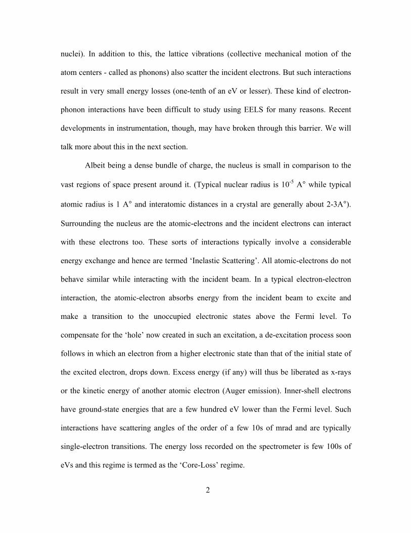
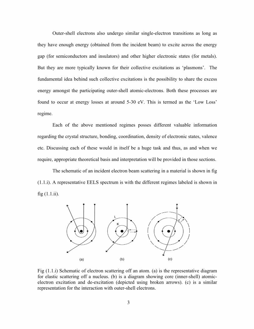
The schematic of an incident electron beam scattering in a material is shown in fig
(1.1.i). A representative EELS spectrum is with the different regimes labeled is shown in
fig (1.1.ii). 1.1 Interaction of Fast Electrons with a Solid 3
Fig. 1.1 A classical (particle) view of electron scattering by a single atom (carbon). (a) Elasticscattering is caused by Coulomb attraction by the nucleus. Inelastic scattering results fromCoulomb repulsion by (b) inner-, or (c) outer-shell electrons, which are excited to a higher energystate. The reverse transitions (de-excitation) are shown by broken arrows
volt and A is the atomic weight of the target nucleus. For E0 = 100 keV, Emax > 1 eVand, in the case of a light element, may exceed the energy needed to displace theatom from its lattice site, resulting in displacement damage within a crystalline sam-ple, or removal of atoms by sputtering from its surface. However, such high-anglecollisions are rare; for the majority of elastic interactions, the energy transfer islimited to a small fraction of an electron volt, and in crystalline materials is bestdescribed in terms of phonon excitation (vibration of the whole array of atoms).
Inelastic scattering occurs as a result of Coulomb interaction between a fast inci-dent electron and the atomic electrons that surround each nucleus. Some inelasticprocesses can be understood in terms of the excitation of a single atomic electroninto a Bohr orbit (orbital) of higher quantum number (Fig. 1.1b) or, in terms ofenergy band theory, to a higher energy level (Fig. 1.2).
Consider first the interaction of a fast electron with an inner-shell electron, whoseground-state energy lies typically some hundreds or thousands of electron voltsbelow the Fermi level of the solid. Unoccupied electron states exist only abovethe Fermi level, so the inner-shell electron can make an upward transition onlyif it absorbs an amount of energy similar to or greater than its original bindingenergy. Because the total energy is conserved at each collision, the fast electronloses an equal amount of energy and is scattered through an angle typically ofthe order of 10 mrad for 100-keV incident energy. As a result of this inner-shellscattering, the target atom is left in a highly excited (or ionized) state and willquickly lose its excess energy. In the de-excitation process, an outer-shell elec-tron (or an inner-shell electron of lower binding energy) undergoes a downwardtransition to the vacant “core hole” and the excess energy is liberated as electro-magnetic radiation (x-rays) or as kinetic energy of another atomic electron (Augeremission).
Fig (1.1.i) Schematic of electron scattering off an atom. (a) is the representative diagram for elastic scattering off a nucleus. (b) is a diagram showing core (inner-shell) atomic-electron excitation and de-excitation (depicted using broken arrows). (c) is a similar representation for the interaction with outer-shell electrons.
4
Fig (1.1.ii) Representative image of an EEL spectrum. The different regions are marked appropriately and the core-loss region magnified in the inset. Since the EEL spectrum is cumulative the background of the spectrum increases with energy loss. 1.2 Nion UltraSTEMTM100MC at ASU
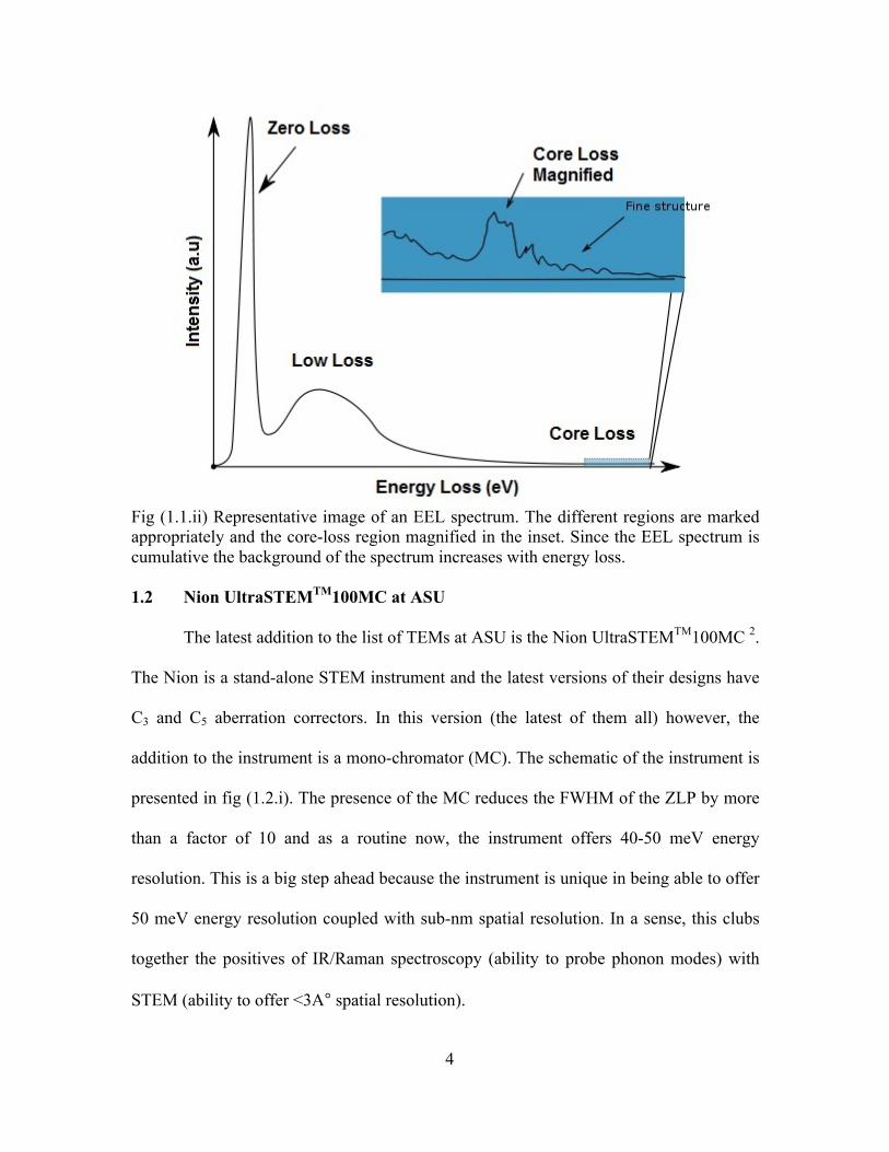
The latest addition to the list of TEMs at ASU is the Nion UltraSTEMTM100MC 2.
The Nion is a stand-alone STEM instrument and the latest versions of their designs have
C3 and C5 aberration correctors. In this version (the latest of them all) however, the
addition to the instrument is a mono-chromator (MC). The schematic of the instrument is
presented in fig (1.2.i). The presence of the MC reduces the FWHM of the ZLP by more
than a factor of 10 and as a routine now, the instrument offers 40-50 meV energy
resolution. This is a big step ahead because the instrument is unique in being able to offer
50 meV energy resolution coupled with sub-nm spatial resolution. In a sense, this clubs
together the positives of IR/Raman spectroscopy (ability to probe phonon modes) with
STEM (ability to offer <3A° spatial resolution).

5
The relevance of this instrument with our work will become obvious in the latter
sections.
Fig (1.2.i) LEFT: Schematic of the Nion UltraSTEMTC100MC installed at ASU. The gun (CFEG) is located at the bottom. The electron beam passes the MC aperture into the slit where the energy selection is made. After narrowing down the beam, it passes through a set of condenser lenses and then the aberration correctors. At this point the beam interacts with the sample and passing through the projector lenses it is received by various detectors. As a typical STEM instrument, it supports ABF, MAADF and HAADF. There is a CCD placed to view the ronchigram and past all that is the ELS detector.
RIGHT: Schematic of the cross-section of the MC showing all lenses and the slit.

6
1.3 Topological Insulators
Topological insulators are a new class of materials identified by the scientific
community as recently as in 2008 3 where the bulk of the material is insulating while the
surface is conducting. Interestingly, one can observe dissipation-less transport of electric
current on any of the 6 surfaces of the material subject to certain conditions. This has
opened a flurry of interesting properties/applications 4 which include:
• Dissipation-less transport
• Spintronics applications
• Fault-tolerant Quantum Computing
• Experimental observation of Majorana Physics
• Topological Superconductors
But the identification of these materials has not been sudden and unexpected. It is
possible to track a serial evolution of the idea of this sort of a property. It all started
with the classical ‘Hall Effect’. On application of an electric field perpendicular to a
magnetic field in a current carrying material, one can observe a voltage drop across
the material in the 3rd direction read as the Hall voltage or the Hall resistance. This
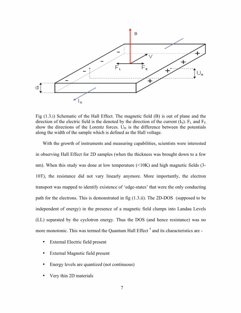
can be observed from fig (1.3.i). The characteristics of Hall Effect are thus –
• External Electric Field present
• External Magnetic Field present
• Continuous Energy Levels observed
• Typically 3D materials.
7
Fig (1.3.i) Schematic of the Hall Effect. The magnetic field (B) is out of plane and the direction of the electric field is the denoted by the direction of the current (IS). FL and FE show the directions of the Lorentz forces. UH is the difference between the potentials along the width of the sample which is defined as the Hall voltage.
With the growth of instruments and measuring capabilities, scientists were interested
in observing Hall Effect for 2D samples (when the thickness was brought down to a few
nm). When this study was done at low temperature (<10K) and high magnetic fields (3-
10T), the resistance did not vary linearly anymore. More importantly, the electron
transport was mapped to identify existence of ‘edge-states’ that were the only conducting
path for the electrons. This is demonstrated in fig (1.3.ii). The 2D-DOS (supposed to be
independent of energy) in the presence of a magnetic field clumps into Landau Levels
(LL) separated by the cyclotron energy. Thus the DOS (and hence resistance) was no
more monotonic. This was termed the Quantum Hall Effect 5 and its characteristics are -
• External Electric field present
• External Magnetic field present
• Energy levels are quantized (not continuous)
• Very thin 2D materials

8
Fig (1.3.ii) Electron Motion in the Quantum Hall Effect. The schematic shows the presence of edge states (propogation of the electrons only on the edge of the 2D system). We can notice that those electrons whose cyclotron orbits are well within the boundaries do not contribute to any current. They become localized and insulating states.
The Quantum Spin Hall (QSH) 6 state is a state of matter proposed to exist in
special, 2D semiconductors with spin-orbit coupling. The QSH is a cousin of the
integer QH state, but, unlike the latter, it does not require the application of a large
magnetic field. It is very important here to note that the QSH state does not break any
discrete symmetries (such as time-reversal or parity) unlike the other previously
mentioned effects.
The first proposal for the existence of a quantum spin Hall state was developed by
Kane and Mele 7 who adapted an earlier model for graphene by Haldane et.al (proposed
in 1988) which exhibits an IQHE. The Kane and Mele model is, two copies of the
Haldane model one over the other, such that the spin up electron exhibits a chiral-IQHE
while the spin down electron exhibits an anti-chiral IQHE. Very recently (in 2006) was a
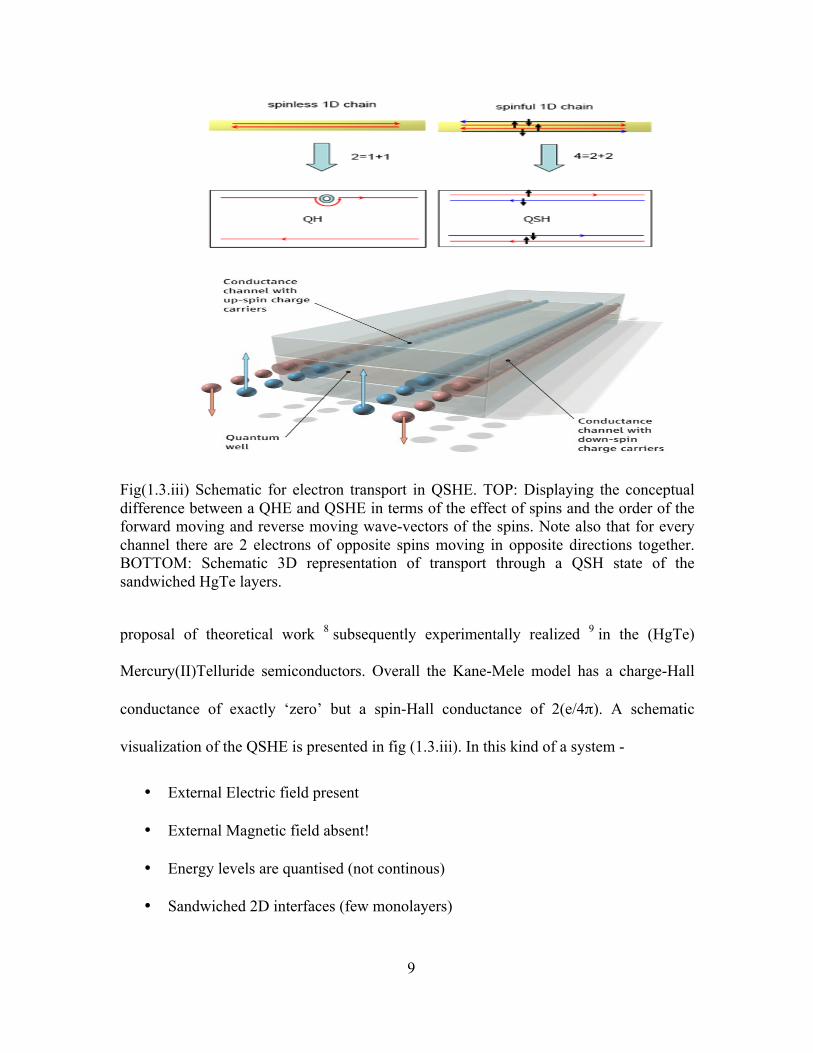
9
Fig(1.3.iii) Schematic for electron transport in QSHE. TOP: Displaying the conceptual difference between a QHE and QSHE in terms of the effect of spins and the order of the forward moving and reverse moving wave-vectors of the spins. Note also that for every channel there are 2 electrons of opposite spins moving in opposite directions together. BOTTOM: Schematic 3D representation of transport through a QSH state of the sandwiched HgTe layers.
proposal of theoretical work 8 subsequently experimentally realized 9 in the (HgTe)
Mercury(II)Telluride semiconductors. Overall the Kane-Mele model has a charge-Hall
conductance of exactly ‘zero’ but a spin-Hall conductance of 2(e/4π). A schematic
visualization of the QSHE is presented in fig (1.3.iii). In this kind of a system -
• External Electric field present
• External Magnetic field absent!
• Energy levels are quantised (not continous)
• Sandwiched 2D interfaces (few monolayers)
10
The concept of topologically protected states as proposed by Kane and Mele 6,10
triggered a lot of interest and opened up the possibility of new materials which could
exhibit similar properties, as mentioned in the above cases, although not necessarily
through the same mechanism. A Topological Insulator (TI) is a material that behaves
as an insulator in its interior or bulk while permitting the movement of charges
(metallic/semi-‐metallic) on its surface. In the bulk of a topological insulator,
the electronic band structure resembles an ordinary band insulator with the Fermi
level in the band gap. On the surface of a topological insulator though, there are
special states that allow surface metallic conduction. Carriers in these surface states
have their spin locked at a right angle to their momentum (spin-‐momentum locking
or topological order). At a given energy the only other available electronic states
have opposite spin, so the "U"-‐turn scattering is strongly suppressed and conduction
on the surface is highly metallic. These states are characterized by an index (known
as Z2 topological invariants) and are an example of topologically ordered states.
Topologically protected edge states (like SQHE) were predicted to occur in quantum
wells (very thin layers) of mercury telluride sandwiched between cadmium telluride and
was observed shortly thereafter. But the surprise came when they were also predicted to
occur in three dimensional bulk solids 11 of binary compounds involving ‘Bismuth’. The
first experimentally realized 3D topological insulator state was discovered in bismuth
antimony 3. The Z2 topological invariants cannot be measured using traditional transport
methods since it requires the separation of surface conduction from that of the bulk.
Hence only a surface characterization technique, like ARPES, could resolve the spin-
sensitive momentum and thereby help differentiate between the bulk and edge states in

11
the system. We can refer to fig (1.3.iv) for the same. Eventually, topologically protected
surface states were also observed in antimony, bismuth selenide, bismuth telluride and
antimony telluride using ARPES.
Fig (1.3.iv) ARPES results on Bi-Sb. A: the number of edge states (corresponds to number of cross-overs and it has to be odd) resolved. B: resistivity measurements done on Bi and Bi0.9-Sb0.1 devices. C: Schematic of the edge state conduction in the Bi-Sb system. (D-I): The Evolution of the Dirac cones in the band structure as the Energy of the probe is altered to resolve the edge state and line-plot along the dotted line.
The surface states of a 3D Topological insulator are thus a new type of 2DEG
(two dimensional electron gas) where electron's spin is locked to its linear momentum. In
a sense it is an extension of the edge-states in a 2D QHE. All the six surfaces possess
these states. The point to note though, is that, the mechanisms for these two processes are

12
not really related. Moreover, although they posses a Dirac-cone like band structure, the
topological surface states differ from Graphene due to the locking of spin and
momentum. Thus as a summary, in characteristics of TIs are:
• External Electric field present
• External Magnetic field absent!
• Energy levels are quantized (not continuous)
• Bulk 3D materials!
1.4 Bismuth Selenide
Bismuth Selenide (Bi2Se3) is a TI with a bulk band gap of around 0.32 eV. It
belongs to the Tetradymite family with an R-3m space group. The lattice parameters are:
a = b = 4.138 A° and c = 28.636 A°. We can refer to Fig (1.4.i) for the unit-cell structure
along specific orientations.
Although it is very recent that Bi2Se3 has been identified as a TI 12, both Bi2Se3
and Bi2Te3 have for long been studied as thermoelectric materials. But Bi2Se3 is a
comfortable candidate to work with because of its relatively higher band gap. Further it
has a single surface state implying simpler detection and analysis of the same. Inherently
it is known to possess two kinds of defects 13 – BiSe (anti-site defects) and VSe (Selenium
vacancies). That apart, researchers have doped Bi2Se3 with various elements as Ca, Mn,
Fe, Cu, Au, Sm etc 14–16, each with a particular property or effect in mind – to reduce the
vacancy induced un-intentional n-doping; to observe the coupled simultaneous behavior
of magnetic and surface effects; to observe variation in thermoelectric coefficients with
interaction/non-interaction of surface states etc. Specifically Cu-Bi2Se3 17,18 displays

13
superconductivity for T < 10K and this is simultaneous to the presence of the surface
states – a topological superconductor! Understanding this is touted to be a big stepping-
stone in realizing quantum computers. This is where our interest in the material arose.
Fig (1.4.i) Bi2Se3 crystal structure. Unit cell viewed along (100). The red atoms correspond to Bi. The dark and light blue atoms correspond to Se (at two non-equivalent sites). The green square and the green stars are the possible sites for dopant atoms to substitute Bi and intercalate in the van der Waals, respectively, gap represented by (b). (a) corresponds to a single set of quintuple layers [Se1-Bi-Se2-Bi-Se1].

14
Very recently a few articles have been published in journals that talk of the issue
of studying Bi2Se3 using TEM and related analytical methods. In the article by Huang et
al. 19, they perform a HAADF-STEM based structural analysis on bulk-grown Bi2Se3 to
identify Bi anti-site defects. This was immediately followed by Liou et al. 20,21 where they
perform angle-resolved TEM-EELS and STEM-EELS experiments on Bi2Se3 to identify
the various peaks in the low-loss regime. They clarify an issue of the 6.3eV plasmon peak
of being bulk in origin (as opposed to prior experiments predicting a surface plasmon
nature). They also perform Molecular Orbital calculations to present a theoretical basis
for their prior claim in the following article. Finally there was a very recent article by Da
et al. 22 where they do HR-TEM studies on Cu-Bi2Se3 and using phase reconstruction
mechanisms they detect the interstitial Copper atoms located in the Bi2Se3 lattice.
Thus, our aim for the experiments boiled down to two big issues – (i) to identify
the position and local environment of the dopant atom (Cu) in the host lattice (Bi2Se3) to
help understand the interaction between magnetic order and topological order and (ii)
understand the effect of local crystal environment on the electronic properties of Bi2Se3
close to the Fermi level. We immediately realized that both these objectives are
obtainable using the EELS technique: the core-loss EELS 23 would provide information
regarding the local environment around the dopant Cu atom – the position, co-ordination,
and valence; the low-loss EELS would provide a list of all the electronic transitions
occurring close the VB-CB region. Thus, the quest to study electronic transitions in
Bi2Se3 and Cu- Bi2Se3 using EELS began…
15
CHAPTER 2
EXPERIMENTS
2.1 Samples, instruments and softwares
The Bi2Se3 and Cu- Bi2Se3 samples were grown using the Bridgeman technique
and obtained from Dr. Yulin Chen from Stanford University (now at Oxford, UK). These
are bulk crystals and the dopant concentration was 2-3%. The reference samples of
99.95% Cu(I)Se were obtained from Sigma Aldrich and 99.5% Cu(II)Se were obtained
from Alfa Aesar. Au-mesh grids of #400 mesh and #1000 mesh were obtained from Ted
Pella and used to deposit the TEM samples of these materials.
The TEM samples were prepared using Leica Ultracut R ultramicrotome. HR-
TEM imaging and TEM-EDS and EELS experiments were performed on the Jeol 2010F.
Most of the HAADF-STEM imaging and STEM-EELS of the Cu(II)Se samples were
done using the Jeol ARM 200F. Some of the HAADF-STEM imaging and STEM-EELS
of Cu(II)Se and all of them for Bi2Se3 were performed on the Nion UltraSTEMTM100MC.
HAADF-STEM image simulations for Cu(II)Se and Bi2Se3 were performed using
the STEMSLICE program from Dr. E. Kirkland. The ELNES and DOS calculations for
the core-loss EELS for Cu(II)Se, Cu(I)Se, Bi2Se3 and Cu- Bi2Se3 were performed using
the FEFF8.4 code.
All EELS data analysis was performed using the Digital Micrograph 2010.
Crystal structure and diffraction simulations were done using the CrystalMaker software
package.

16
2.2 TEM Sample preparations
Bi2Se3 is anisotropic (as can be observed from the unit cell parameters) and is
weakly bonded in the c-axis (van der Waals force between each quintuple layer).
Therefore, similar to Graphene, it can be easily exfoliated along the a-b plane. This
makes it tough to prepare TEM samples because polishing these samples will crush/break
them very easily. FIB and other such milling processes induce a lot of damage (and
defects) to the sample thus altering their structural character. Moreover the samples are
not grown on a substrate (these are bulk grown). So it is all the more vulnerable to losing
integrity. Thus we had to identify a method of sample preparation that can utilize this as
it is and yet make samples that are thin enough to be studied by HRTEM and STEM. This
is when we stumbled upon ‘Ultramicrotomy’.
As we can see in fig (2.2.i), ultramicrotomy is the process of using a
diamond/glass knife to manually/automatically cut thin sections of a given material. This
follows two steps – (i) To embed the material in a resin and then let it age for a couple of
days to harden as a matrix. (ii) To position this matrix on the microtome stage and then
set the knife to cut through this matrix (cutting sections of the resin+material). Prior
knowledge of the orientation of the material can help in suitably embedding it in the resin
so that when the sections are cut, they are very close to the required directions. Further,
the sample holder is generally fitted with a vernier gauge that permits to change the angle
of the sample with respect to the knife in 2 directions in the plane parallel to the knife.
Once this is fixed and calibrated, the first sections of the material is cut at larger
thicknesses (200nm-500nm) to get a feel of the friction offered on the knife as it passes
through the region with the material. At this point if there is no harm happening to the

17
sections, then it is safe to turn the vernier lower so as to obtain thinner sections. The
instrument we use, Leica Ultracut R, can produce sections of the order of 20 – 30 nm
consistently. Below this is not consistent and not predictable. It is very important to
choose the right resin to as a matrix to host the desired material. The criterion to be
looked at is the hardness of sample must be comparable to the hardness of the resin.
Fig (2.2.i) Schematic of the microtome knife and the stage. A: Sample stage. B: Manual knob which on rotation (clockwise) brings the sample-stage down and then raises it back up. C: Sample (resin+material) set on the sample stage. D: Diamond/Glass knife. E: Sections coming off the knife edge and collection into the hollow filled with water. Eventually the TEM grid is dipped from a side, beneath the sections, to collect them on the grid. Use a small filter paper to remove excess water and the sample is ready for TEM analysis.

18
Ultramicrotomy is typically used for polymers, biological materials and other
soft-materials that cannot withstand traditional polishing and/or milling techniques used
to prepare TEM samples. A very big advantage of the method is that it uses substantially
less raw material to prepare the final sample in comparison to polishing methods.
For our work, all our samples were prepared using this method. The resin we used
is Epon and we prepared both plan-view and cross-sections of Bi2Se3, Cu-Bi2Se3, Cu(I)Se
and Cu(II)Se.
2.3 2010F and Core-Loss EELS
2.3.1 Preliminary TEM
Once the samples are ready, we take them to the Jeol 2010F instrument. Typically
this sample is spread out over large regions. And so to start with the high-mag mode
might not be a good idea. It is important to identify the sample regions and then
increment in magnification. A very important step here is to get used to the difference
between strips of resin sections and strips of sample sections. Simple logic will guide us
to realize that the scattering of the sample region will be stronger and so in BF imaging,
the material of interest (Bi2Se3 or Cu-Se) will appear much darker than the resin.
Fig (2.3.1.i) shows relatively low-mag images of the sample on the mesh-grids. It
is important to note here that although the sample might have been identified, there might
still be resin beneath the sample. Depending on how thick the resin layer beneath is, it
might/might not affect spectroscopic information obtained from the sample region. So it
is important to be patient in finding a good region with minimal/no resin (carbon) layers
beneath the material.
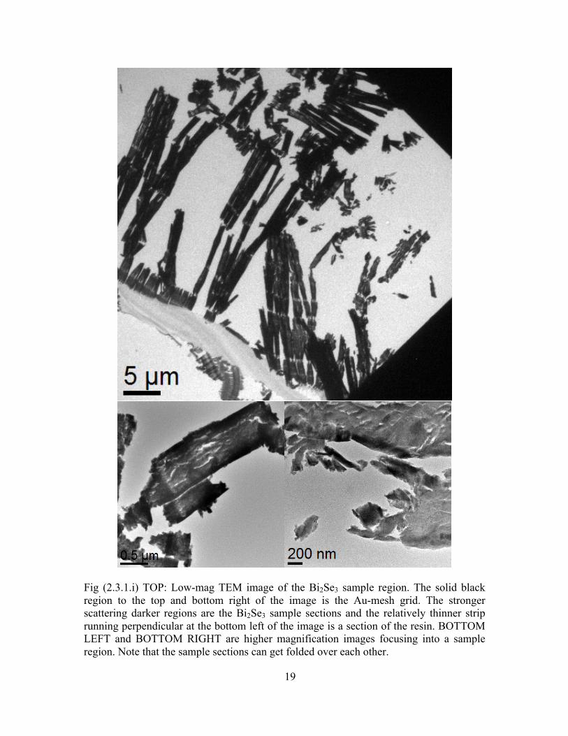
19
Fig (2.3.1.i) TOP: Low-mag TEM image of the Bi2Se3 sample region. The solid black region to the top and bottom right of the image is the Au-mesh grid. The stronger scattering darker regions are the Bi2Se3 sample sections and the relatively thinner strip running perpendicular at the bottom left of the image is a section of the resin. BOTTOM LEFT and BOTTOM RIGHT are higher magnification images focusing into a sample region. Note that the sample sections can get folded over each other.

20
Fig (2.3.1.ii) HRTEM images at high-mag of cross-sectional Bi2Se3. Sample prepared using TOP: 25nm sections and BOTTOM: 50nm sections. Notice the intereference patterns reflecting the quintuple layer sequence in both images. Neither of the images were taken at a ZA orientation.

21
Fig (2.3.1.iii) EDS spectrum of Cu-Bi2Se3. Sample N3D region-1 showing clear indication of Cu-Kα peak and thus presence of Cu. It also highlights Se-Lα, Bi-Lα, Au-Lα, Bi-Lβ, Au-Lβ peaks amongst others. Note that some of the peaks are very close and hence overlap. Hence its imperative to find peaks without overlaps for quantitative analysis (if any).

22
HRTEM images of two different such regions on two different samples are shown
in fig (2.3.1.ii). One of them is obtained out of microtome sections of 50nm and the other
25 nm as mentioned in the figure. Note the image displaying interference patterns
showing the quintuple layer sequence. These are cross-sectional samples of Bi2Se3.
For the Cu- Bi2Se3 samples, before we jump into EELS analysis of the core-loss
regions, it is very important to identify first whether or not we can detect copper. And it
is easily done using preliminary check with the EDS. Fig (2.3.1.iii) is a typical example
of EDS data indicating the presence of Cu. The other peaks corresponding to the Au-grid,
Bi and Se are also highlighted. Once this is done, we are ready to perform EELS
experiments.
2.3.2 Core Loss EELS
In the interest of answering our second objective, we started with obtaining EELS
spectra from Cu-Bi2Se3. We noticed a specific nature of the NEFS. There are quite a few
articles in literature 24,25 that insist on a Cu+1 valence state for the interstitial doping and
we decided to verify this claim too. Moreover core-loss information could also help us
understand why on doping Cu (and to specific sites), the system turns topologically
superconducting 26. An important point to note here is that our initial attempts were at
comparing the Cu-L3 edge of Cu-Bi2Se3 with that of the respective oxides Cu(I)O and
Cu(II)O. The match was very poor and we immediately realized this was a bad
comparison because although the valence states may be similar, the Cu-O system and Cu-
Se system were very different. Thus, we ordered reference samples of Cu(I)Se and
Cu(II)Se. Fig (2.3.2.i) shows typical experimental Cu-L3 edge obtained from EELS in
diffraction mode. This is obtained for Cu-Bi2Se3, Cu(I)Se and Cu(II)Se.

23
Fig (2.3.2.i) Experimental Cu-L3 edge for Cu-Bi2Se3, Cu(I)Se and Cu(II)Se. From direct comparison of the three spectra it is not very easy to determine whether the blue spectra matches with red and green more. This may also suggest that Cu in Bi2Se3 might be a mixed valence state in between +1 and +2.
Right at this point we realized that TEM-EELS will not suffice to elaborate on the
valence of Cu or its location in the atomic lattice. Instead, it led to more questions: (i) Is
the valence closer to +1 or +2 or a mixed state of both? (ii) Is it first theoretically
practical to embark on this experiment?
To answer these questions, we delved deeper into the core-loss analysis.

24
CHAPTER 3
CORE-LOSS ANALYSIS
3.1 Simulations
The moment we saw that after our first set of experiments we had more questions
surrounding us, than answers, we decided that we must try to computationally attack this
issue and understand what is at stake. So the first issue at hand was to simulate the NEFS
for Cu for all the various systems we have and understand them.
3.1.1 FEFF8.4
The FEFF8.4 code 27,28 is a package that calculates the X-ray Absorption near-edge
structure. The input for this code is generated by ATOMS program. What ATOMS does
is generate atomic co-ordinates when crystallographic data about the crystal in question is
fed as input. Now, the FEFF generated XANES spectrum is equivalent of EELS for x-
rays and the LDOS that it calculates is the density of unoccupied states in the crystal. The
FEFF code works on the RSMS technique in which it considers the atom of our choice as
the central atom from which a spherical wave emanates. This wave, in its path outward,
interacts with all its neighbors and thus reflects the 3 most important parameters that we
are interested in, from an EEL spectrum:
a) Nature of neighbor (what element) - through the respective atomic potential
b) Nature of co-ordination (tetrahedral/octahedral) – spatial arrangement of atoms
c) Neighbor distance (bond length) – how strong/weak the interaction is.

25
3.1.1.1 ELNES
As mentioned earlier, the XANES output of the FEFF code is equivalent to the
ELNES. So we start with the aim of simulating the Cu-L3 ELNES for Cu(I)Se and
Cu(II)Se so that we can use these to at least predict using simulations of the qualitative
(and if possible quantitative) differences in the respective spectra amongst each other and
with Cu-Bi2Se3. Interestingly, we observe that for every non-equivalent crystallographic
position of an element, there is an associated NEFS that is unique to that position (as
would be expected since the above mentioned three parameters would be different). Thus
the overall NEFS of the system would be the weighted sum of all these states.
For ex: In Cu(II)Se there are two non-equivalent Cu sites (labeled Type A and Type
B) in the unit cell, thus displaying two different NEFS [as in fig (3.1.1.1.i)]. And the
cumulative spectrum (as it would be) is shown as W.A x 1.75 (multiplied by a factor to
plot it in a manner easy for comparison). The same is also done for Cu(I)Se. In this
system, there are ‘twelve’ different sites of Copper. But they have been clubbed into four
different types (Type: A, B, C and D) putting together sites with similar nearest neighbor
co-ordination under one type. And looking at fig (3.1.1.1.ii) one can observe a similar
variation in the NEFS of Cu for each of the types and also the overall spectrum as a
weighted average. Here the overall spectrum has been shown as W.A x 1.4.
The above observation makes for an interesting argument since, it has been
commonly presumed (as mentioned earlier) in many articles 24,25 that the ‘Cu+1’ state
contributes to doping in the intercalating regions in the Van der Waals gap. And this is
also the specific site that contributes to the superconductivity at low temperatures in this
otherwise non-superconducting system (at 5-10K).

26
Fig (3.1.1.1.i) FEFF8.4 simulations of Cu-L3 edge for Cu(II)Se. Type A and Type B refer to the two non-equivalent Cu atoms as the central atom for the calculation respectively. W.A refers to the weighted average of the aforementioned mentioned spectra which represents the overall spectrum. It is multiplied by a factor of 1.75 only for display. Notice the intensities of the two major peaks are completely reversed for the two cases!
EELS based valence determination for 3d elements 29,30 is a commonly found procedure,
though in this case clearly, the NEFS cannot be attributed to a particular valence since it
is not a one-one relation. Moreover, it also calls for a possible nearest neighbor co-
ordination based classification of the dopant site, which would be more reliable and
specific.

27
Fig (3.1.1.1.ii) FEFF8.4 simulations of Cu-L3 edge for Cu(I)Se. Type A through D refer to the 12 different Cu atoms grouped together into four categories, that are each framed as the central atom for the calculation respectively. Like in Fig (3.1.1.1.i) W.A refers to the weighted average of the aforementioned mentioned spectra which would represent the bulk spectrum of Cu(I)Se. it is multiplied by a factor of 1.4 only for display.
3.1.1.2 DOS
FEFF8.4 apart from providing the NEFS for the central atom also provides the
local density of states (DOS) for each element and for each orbital (s/p/d). We know that
the NEFS in EELS/XAS is a direct consequence of the LDOS of the system. Thus it
makes a good venture to analyse the LDOS and TDOS for the various cases mentioned
below since that will help us understand what are the interacting orbitals and what is the
28
nature of interaction. Since the system in concern is Cu as central atom surrounded by Se
and Bi atoms as the nearest neighbors, our subsequent interest was in simulating the L-
DOS and T-DOS for various cases of neighbor co-ordination.
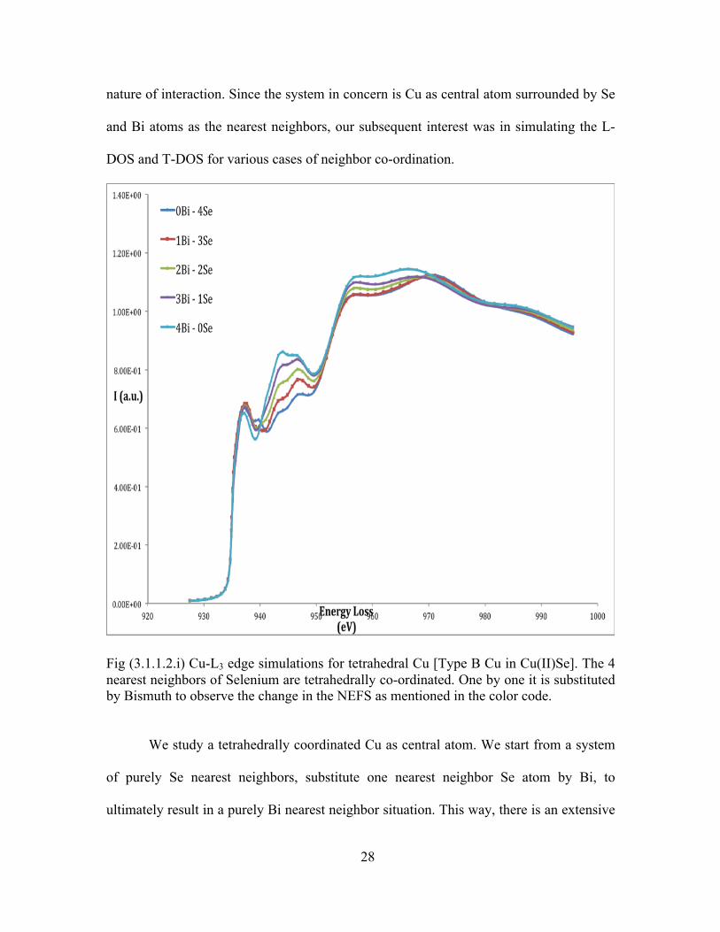
Fig (3.1.1.2.i) Cu-L3 edge simulations for tetrahedral Cu [Type B Cu in Cu(II)Se]. The 4 nearest neighbors of Selenium are tetrahedrally co-ordinated. One by one it is substituted by Bismuth to observe the change in the NEFS as mentioned in the color code.
We study a tetrahedrally coordinated Cu as central atom. We start from a system
of purely Se nearest neighbors, substitute one nearest neighbor Se atom by Bi, to
ultimately result in a purely Bi nearest neighbor situation. This way, there is an extensive

29
library of NEFS and associated DOS for almost all possible cases of the specific
coordination.
Fig (3.1.1.2.ii) Partial (s, p, d) and total DOS simulations for tetrahedral Cu [Type B Cu in Cu(II)Se]. The 4 nearest neighbors of Selenium are tetrahedrally co-ordinated. One by one it is substituted by Bismuth to observe the change in the NEFS as mentioned in the color code. This figure goes in correlation with the NEFS simulations done in Fig (5). The dotted line marked in black denoted by Ef is the Fermi Energy. The Intensities are in arbitrary units and are adjusted so as to present the necessary features as best as possible. The Total DOS is the sum of the individual DOS for each particular case.
30
In fig (3.1.1.2.i) we present the ELNES simulations and in Fig (3.1.1.2.ii) the
corresponding s-DOS, p-DOS, d-DOS and T-DOS for the case of tetrahedrally
coordinated Cu(II)Se (with type B Cu as central atom). From the two figures, we can
easily find the correlation of what we observe in the ELNES to what changes happen in
the DOS. This will be held as a reference, which we will utilize when we can discover the
nearest neighbor co-ordination in the actual system of interest Cu-Bi2Se3. Depending
upon our observation from the experiments, if required, we might do a similar simulation
series for the octahedral Cu system - substituting the Se atoms one by one with Bi.
The two issues that are very clear from simulations are – (a) that each non-
equivalent site of Cu can possibly have a very different NEFS and so it will be wrong to
advocate a valence comparison. Rather, for each different co-ordination, the NEFS will
be unique and that would be a good standard. (b) Cu with majority Bi and Bu with
majority Se neighbors have very different NEFS structures for the major two peaks after
the edge. So obtaining a spectrum from Cu-Bi2Se3 and noticing the nature of the near-
edge structure can be used to close in on the ideal co-ordination in the material of
interest.
But before we push on to experiments, we have one more set of simulations to
perform for comparison. And these must be the HAADF-STEM simulations for Cu(II)Se
and Bi2Se3.

31
3.1.2 STEMSLICE
Simultaneous to the FEFF simulations, we also carried out STEM-HAADF image
simulations using the STEMSLICE code to have an idea of what to expect in our actual
experiments. Our motivation here is bi-directional:
• HAADF-STEM image simulation of Bi2Se3 – aligned with the primary goal of
STEM-EELS experiments on Cu-Bi2Se3 [fig (3.1.2.i)].
• HAADF-STEM image simulation of Cu(II)Se – to distinguish the two non-
equivalent Cu sites. Would be eventually useful if STEM-EELS from both these
Cu sites were to be obtained experimentally [fig (3.1.2.ii)].
Fig (3.1.2.i) STEMSLICE simulation of HAADF-STEM images for cross-sectional Bi2Se3: Columns are well resolved. Brighter dots correspond to Bi and fainter dots correspond to Se. The red box denotes one quintuple layer of [Se-Bi-Se-Bi-Se]. Region between the two successive faint dots is the van der Waals region. Simulation parameters: Projection = <100>; Eo = 200kV; Cs = 0.00mm; df = 0.00 A⁰; Aperture = (0, 10.37) mrad; Size of ψprobe: 256 x 256 pixels.
In the case of Bi2Se3 the atoms are clearly visible and thanks to the relatively
large inter-atomic distances, the atoms are well separated. But as is visible in fig (3.1.2.i),
83Bi being a huge atom scatters much stronger than 34Se. In the eventuality of studying
Cu-Bi2Se3, 29Cu being the lightest element of the three, would probably be difficult to

32
identify purely through HAADF-STEM. The simulations thus present us a point of
concern, a way to get over which would be HAADF-STEM + EDS/EELS.
Fig (3.1.2.ii) STEMSLICE simulation of HAADF-STEM images for cross-sectional Cu(II)Se: dumbbells observed. Relatively bigger atom in the dumbbell is Se. Inclined dumbbells contain Cu Type A and Vertical (horizontal) dumbbells contain Cu Type B. Note that Cu type A and Cu type B actually end up closer together in this orientation. Simulation parameters: Projection = <100>; Eo = 200kV; Cs = 0.00mm; df = 0.00 A⁰; Aperture = (0, 10.37) mrad; Size of ψprobe: 256 x 256 pixels.
For the Cu(II)Se, the simulations show us that the Cu and Se atoms are too close
to be separated perfectly. This means that we should be expecting a dumbbell like
structure in our experiments too. But the two different Copper sites are a part of two
different dumbbells and thus well differentiated. Thus if we can obtain EELS spectra
from dumbbell set that are horizontal and those that are inclined separately, we must
ideally be able to obtain two different Cu L3 NEFS.
Here we would like to mention that we do not perform these simulations for
Cu(I)Se. The reason to go only with Cu(II)Se was because, it seemed practically easier to
work on Cu(II)Se considering it has only ‘two’ non-equivalent Cu sites within its unit cell
as opposed to Cu(I)Se that has ‘twelve’.

33
3.2 AC-STEM
With the simulation of the HAADF-STEM images and the NEFS and DOS with
us, we first utilized the JeoL ARM200F instrument. It has a Cs corrector installed. This is
TEM/STEM instrument and has significantly higher current in the STEM mode than the
Nion UltraSTEMTM100MC. Our aims getting into the experiments were:
• HAADF-STEM (EELS) on Cu(II)Se – To separate the two Cu sites and if
possible obtain the individual EELS spectra from the respective sites.
• HAADF-STEM (EELS) on Cu-Bi2Se3 – Aligned with the primary aim to identify
the site occupancy of Cu and also the nature of the Cu-NEFS (in this case atomic-
column resolved).
Figure (3.2.i) AC-STEM HAADF image of Cu(II)Se. LEFT: The image within the yellow box is the superimposed STEMSLICE simulation. It shows a very good match with experimental result. The two ROIs are the line plots integrated over a thickness of 20 units and their respective plots are on the RIGHT side of the HAADF image. The dumbbells are well resolved and going by the intensity variation, the smaller intensity corresponds to Cu and vice versa, as has been labeled in the line plots. The order of atom arrangement within the dumbbell is also visible thus.

34
Fig (3.2.i) shows a HAADF-STEM image of Cu(II)Se and a line profile from the
image resolving the two dumbbells into their respective Se and Cu peaks. This can be
compared with the STEMSLICE simulations performed (as in previous section) and are
observed to match very well. We can also notice the stronger and weaker reflections in
the dumbbells in the experiments as in our simulations. We would like to mention here
that although in the line-plots that we show here, the intensity variation is clear and looks
consistent, it is not the case for every region even within the displayed image fig (3.2.i).
We think this is because, locally, not every region is perfectly aligned to the ZA. This is
common in microtome prepared samples as compared to mechanically polished samples.
Having resolved the two Cu sites in Cu(II)Se, we were now interested in trying to
obtain the NEFS data from the two different Cu sites that could potentially not just
spatially resolve the Cu, but also attribute their individual and unique electronic structure
identities. Albeit our efforts, for now, we have not been able to obtain any significant
difference in the NEFS of the two different types of Cu. We strongly believe that this
could be due to the much attributed ‘cross-talk’ between neighboring atomic columns that
are not so far from each other (in this case around 2.2 A° apart). This has been explained
in detail in the work by Dr. Rossouw 31,32 and Dr. Steve Pennycook’s group 33. Our case
being further hindered since both the dumbbells in question contain Cu, the intensity of
the Cu NEFS will not reduce/increase dramatically enough to observe a difference. Fig
(3.2.ii.TOP) shows the two survey image with the two different EELS acquisition regions
and fig (3.2.ii.BOTTOM) is both these spectra overlaid – no appreciable difference at all!

35
Figure (3.2.ii) STEM-EELS on Cu(II)Se. TOP: AC-STEM HAADF survey image of Cu(II)Se for EELS data acquisition. The green and the blue ROIs are respectively the inclined and the horizontal regions containing the two different types of Cu [as in fig (3.2.i)]. BOTTOM: The background subtracted EEL spectra of the respective cases. The two individual spectra (green and blue) are overlaid. Clearly there is no observable difference in intensity, peak width or nature/position of the peaks.
36
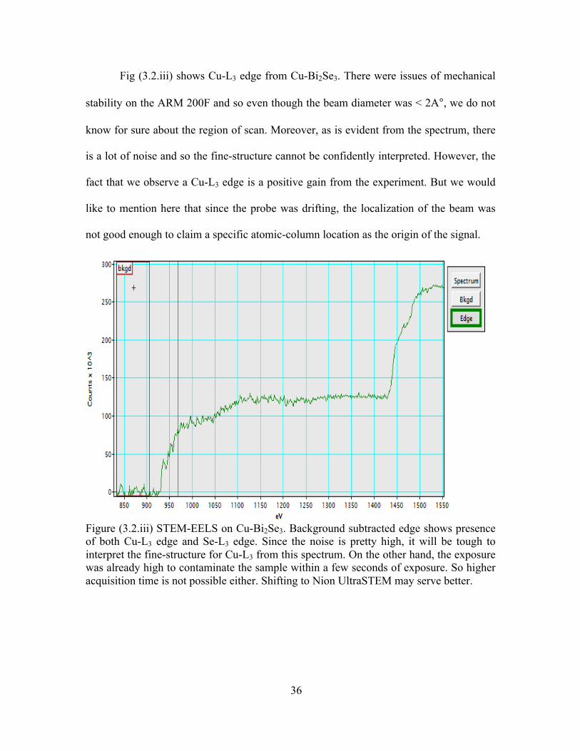
Fig (3.2.iii) shows Cu-L3 edge from Cu-Bi2Se3. There were issues of mechanical
stability on the ARM 200F and so even though the beam diameter was < 2A°, we do not
know for sure about the region of scan. Moreover, as is evident from the spectrum, there
is a lot of noise and so the fine-structure cannot be confidently interpreted. However, the
fact that we observe a Cu-L3 edge is a positive gain from the experiment. But we would
like to mention here that since the probe was drifting, the localization of the beam was
not good enough to claim a specific atomic-column location as the origin of the signal.
Figure (3.2.iii) STEM-EELS on Cu-Bi2Se3. Background subtracted edge shows presence of both Cu-L3 edge and Se-L3 edge. Since the noise is pretty high, it will be tough to interpret the fine-structure for Cu-L3 from this spectrum. On the other hand, the exposure was already high to contaminate the sample within a few seconds of exposure. So higher acquisition time is not possible either. Shifting to Nion UltraSTEM may serve better.

37
CHAPTER 4
LOW LOSS ANALYSIS
4.1 AC-STEM
Apart from the interest in studying the core-level excitations in doped TIs, as has
been mentioned right at the beginning, our interest is also in studying the vibrational and
low-loss spectrum of Bi2Se3. As mentioned in the introduction, Bi2Se3 has a band gap of
around 0.32eV and most of its optical phonon modes exist at <20 meV. Although the
Nion UltraSTEM 2,34 has demonstrated capabilities of very high-energy resolution
(30meV consistently), peaks around 50meV and lower (in absolute values of abscissa)
would be nearly impossible to study because of the presence of the ZLP and its tail. But
as can be seen in 20, there are lots of interesting electronic transitions happening in the
low-loss regime. Moreover, this material has not been studied in such great detail using
high resolution (S)TEM. So most of the electronic structure studies are from 70s and 80s.
Bi2Se3 is known to have defects and although there is a moderate idea of the effect of the
defects (anti-site BiSe and vacancies VSe) 35, there is no study that specifically targets this
issue to reports on the effect of the defects on the electronic states close to VB using a
TEM. And apart from all these aspects, doping the Bi2Se3 sample can (and does) change
the electronic structure around the valence band (since most of the electron transport
happens from this region). Thus we pursued low-loss regime electronic-transition studies
in Bi2Se3.
Fig (4.1.i) is a HAADF-STEM image of the sample with the STEMSLICE
simulated image overlaid. The experimental atom centers are marked with red (Bi) and
blue (Se) dots to visualize how good the agreement is qualitatively. Again, a point to note

38
is that since the samples are made by microtomy, very small and local changes in
orientation is possible, thus shifting away from the ZA and hence not being perfectly
aligned.
Fig (4.1.i) Experimental HAADF-STEM image of cross-sectional Bi2Se3. LEFT: Area 1 raw HAADF-STEM image and RIGHT: Area 2 smoothed-image with Inset on top left as the raw image. Overlaid image is STEMSLICE simulated image for both areas. Bright spots on the experimental image correspond to Bi, the other corresponds to Se. Experiment Parameters: E = 100keV; MC not inserted; Convergence Semi-angle = 30mrad; Beam Current = 70-80 pA; Probe Size ≈ 1.2 A° Simulation Parameters: E = 200 keV; Cs = 0mm; df = 0 A°; Aperture = 0, 10.4mrad; Size of probe ψ (Nx, Ny) = 512x512 pixels; Collection Detector = 50, 200 mrad; (xi, xf, yi, yf, Nxout, Nyout) = (0, 28, 0, 10.6, 64, 64).
Similar to 20 we also performed low-loss measurements at 0.02ev/channel and
0.1ev/channel. It was necessary to use a lower dispersion to obtain a bigger range on the
energy loss. Choosing a higher dispersion gave higher resolution but the energy loss
range was smaller due to the fixed number of pixels on the detector. As we can see in fig
(4.1.ii.a and 4.1.ii.b), we are able to identify various kinds of electronic transitions like

39
Fig (4.1.ii) Experimental low-loss STEM-EELS of Bi2Se3. A: Raw spectrum showing 5 peaks:- (e) is the Bi-O4,5 peak. (d) and (b) are π+σ and the π bulk plasmons respectively. (c) is predicted to be a surface plasmon. (a) is unknown at 2.5-2.8eV. B: Background subtracted spectrum with peaks (e) as above, and (f) as the Se-M4,5 peak. Inset in the bottom-right shows the raw image. Experiment Parameters: E = 100keV; MC inserted!; Convergence Semi-angle = 30mrad; EELS Collection angle = 15 mrad; Energy Resolution = 30 – 50 meV (ZLP FWHM); Beam Current = 50-70 pAmp; Probe Size ≈ 1.5 A°

40
the bulk plasmons (b) and (d); surface plasmons (c); O4,5 edge of Bismuth (e) and M4,5
edge of Selenium (f). There is also a peak (a) at around 2.5-2.8eV whose origin is
unknown to us for now. The Bi-O4,5 edge is actually very well observed in this spectrum.
Operating at the best energy resolution possible of around 40meV and
0.003eV/channel, we tried to observe the phonon region of the low-loss i.e. < 2eV (and
specifically <0.5eV). We found an interesting feature as a shoulder on the tail of ZLP.
We repeated the experiments and found it to be around the same value of roughly
0.32eV! We predict this to be the band-gap in which case it will be the first ever
successful demonstration of identifying a band-gap at such low eV using a TEM.
We would like to highlight the figure (4.1.iii) all together to mention a few things.
In spectrum (4.1.iii.a) the peak labeled (g) corresponds to the band-gap and the same
peak post background subtraction of the ZLP is as observed in fig (4.1.iii.c). Figure
(4.1.iii.b) is the ZLP recorded just before the measurement was made and it shows a
FWHM (Δ) of 0.045eV (45 meV). In spite of that, we can still see a bulge on the lower
end of the ZLP and this is probably due to aberrations that could not be corrected for
during ELS spectrometer alignment.

41
Fig (4.1.iii) Experimental Zero-Loss region STEM-EELS of Bi2Se3. TOP: Raw spectrum showing (g) band-gap transition peak. BOTTOM LEFT: background subtracted data of A clearly showing the transition at 0.32eV. BOTTOM RIGHT: ZLP measured just before the spectrum A was measured. Δ (FWHM) = 45meV and * is tail broadening due to ELS spectrometer aberration. Experiment Parameters: E = 100keV; MC inserted!; Convergence Semi-angle = 30mrad; EELS Collection angle = 15 mrad; Energy Resolution = 30 – 50 meV (ZLP FWHM); Beam Current = 50-70 pAmp; Probe Size ≈ 1.5 A°

42
CHAPTER 5
CONCLUSIONS AND FUTURE ROADMAP
5.1 CONCLUSIONS
• Successful realization of TEM sample preparation process using ultramicrotome
for Bi2Se3, Cu(I)Se and Cu(II)Se bulk crystals.
• Core-loss EELS in diffraction mode shows the dopant Cu does not match closely
with Cu+1 or Cu+2 valence state.
• FEFF8.4 simulations reveal that every non-equivalent site possesses a unique
NEFS. Thus, the overall FS for an atom in a crystal is a weighted average of such
individual contributions. This means, classification based on co-ordination is a
better and unique standard.
• Core-Loss (AC)STEM-EELS of Cu(II)Se shows cross-talk of the two copper
sites.
• Low-Loss (AC)STEM-EELS using Nion reveals band-gap of Bi2Se3! And many
other electronic transitions.
5.2 FUTURE ROADMAP
• Angle-resolved EELS in Nion-UltraSTEM to study unknown peak (a).
• Effect of doping on the low-loss inter/intra band transitions
• Study alternative (heavy) dopants to obtain HAADF-STEM images of dopant
atomic positions.
• Correlate core-loss simulations using FEFF and STEM-EELS from Cu-Bi2Se3 to
predict co-ordination around dopant atom.

43
REFERENCES
1. Egerton, R. F. Electron Energy-Loss Spectroscopy in the Electron Microscope. (Plenum Press, New York, 1996).
2. Krivanek, O. L., Lovejoy, T. C., Dellby, N. & Carpenter, R. W. Monochromated STEM with a 30 meV-wide, atom-sized electron probe. Journal of electron microscopy 62, 3–21 (2013).
3. Hsieh, D. et al. A topological Dirac insulator in a quantum spin Hall phase. Nature 452, 970–4 (2008).
4. Qi, X.-L. & Zhang, S.-C. Topological insulators and superconductors. Reviews of Modern Physics 83, 55 (2010).
5. Klitzing, K. v., Dorda, G. & Pepper, M. New method for high accuracy determination of fine-struture constant based on quantized hall resistance. Physical Review Letters 45, 11–14 (1980).
6. Kane, C. L. & Mele, E. J. Z_{2} Topological Order and the Quantum Spin Hall Effect. Physical Review Letters 95, 146802 (2005).
7. Kane, C. L. & Mele, E. J. Quantum Spin Hall Effect in Graphene. Physical Review Letters 95, 226801 (2005).
8. Bernevig, B. A., Hughes, T. L. & Zhang, S.-C. Quantum spin Hall effect and topological phase transition in HgTe quantum wells. Science (New York, N.Y.) 314, 1757–61 (2006).
9. König, M. et al. Quantum spin hall insulator state in HgTe quantum wells. Science 318, 766–70 (2007).
10. Fu, L., Kane, C. & Mele, E. Topological Insulators in Three Dimensions. Physical Review Letters 98, 106803 (2007).
11. Qi, X. & Zhang, S. The quantum spin Hall effect and topological insulators. Arxiv 1001.1602v1 (2010).
12. Zhang, H. et al. Topological insulators in Bi2Se3, Bi2Te3 and Sb2Te3 with a single Dirac cone on the surface. Nature Physics 5, 438–442 (2009).
13. Horak, J., Stary, Z., Lostak, P. & Pancir, J. ANTI-SITE DEFECTS IN n-Bi,Se, CRYSTALS. J. Phys. Chem. Solids 51, 1353–1360 (1990).

44
14. Hor, Y. S., Checkelsky, J. G., Qu, D., Ong, N. P. & Cava, R. J. Superconductivity and non-metallicity induced by doping the topological insulators Bi2Se3 and Bi2Te3. J Phys Chem Solids 72, 572 (2011).
15. Salman, Z. et al. The Nature of Magnetic Ordering in Magnetically Doped Topological Insulator Bi_2-xFe_xSe_3. Arxiv Preprint 1203.4850 (2012). at <http://arxiv.org/abs/1203.4850>
16. Zhang, D., Richardella, A., Xu, S. & Rench, D. W. Interplay between ferromagnetism, surface states, and quantum corrections in a magnetically doped topological insulator. Cond Mat arxiv:1206, 1–18 (2012).
17. Hor, Y. S. et al. Superconductivity in Cu_{x}Bi_{2}Se_{3} and its Implications for Pairing in the Undoped Topological Insulator. Physical Review Letters 104, 057001 (2010).
18. Wray, L. A. et al. Observation of topological order in a superconducting doped topological insulator. Nature Physics 6, 855–859 (2010).
19. Huang, F.-T. et al. Nonstoichiometric doping and Bi antisite defect in single crystal Bi_{2}Se_{3}. Physical Review B 86, 081104 (2012).
20. Liou, S. C. et al. Plasmons dispersion and nonvertical interband transitions in single crystal Bi_{2}Se_{3} investigated by electron energy-loss spectroscopy. Physical Review B 87, 085126 (2013).
21. Shu, G. J., Liou, S. C. & Chou, F. C. π -bonds in graphene and surface of topological insulator Bi2Se3. Arxiv 1–5 (2013).
22. Das, T., Bhattacharyya, S., Prakash Joshi, B., Thamizhavel, A. & Ramakrishnan, S. Direct evidence of intercalation in a topological insulator turned superconductor. Materials Letters 93, 370–373 (2013).
23. Tafto, J. & Zhu, J. Electron Energy Loss Near Edge Structure (ELNES), A potential technique in the studies of local atomic arrangements. 9, 349–354 (1982).
24. Kriener, M. et al. Electrochemical synthesis and superconducting phase diagram of Cu_{x}Bi_{2}Se_{3}. Physical Review B 84, 054513 (2011).
25. Vasko, A., Tichy, L., Horak, J. & Weissenstein, J. Amphoteric nature of copper impurities in Bi2Se3 crystals. Appl. Phys 5, 217–221 (1974).
26. Bray-Ali, N. & Haas, S. How to turn a topological insulator into a superconductor. Physics 3, 11 (2010).

45
27. Ankudinov, A. L., Ravel, B., Rehr, J. J. & Conradson, S. D. Real-space multiple-scattering calculation and interpretation of x-ray-absorption near-edge structure. 58, 7565–7576 (1998).
28. Moreno, M. S., Jorissen, K. & Rehr, J. J. Practical aspects of electron energy-loss spectroscopy (EELS) calculations using FEFF8. Micron (Oxford, England : 1993) 38, 1–11 (2007).
29. Paterson, J. H. & Krivanek, O. L. ELNES OF 3d TRANSITION-METAL OXIDES H. Variations with oxidation state and crystal sffucture James H. PATERSON. Ultramicroscopy 32, 319–325 (1990).
30. Wang, Z., Yin, J. & Jiang, Y. EELS analysis of cation valence states and oxygen vacancies in magnetic oxides. Micron (Oxford, England : 1993) 31, 571–80 (2000).
31. Findlay, S. D., Allen, L. J., Oxley, M. P. & Rossouw, C. J. Lattice-resolution contrast from a focused coherent electron probe. Part II. Ultramicroscopy 96, 65–81 (2003).
32. Rossouw, C. J., Allen, L. J., Findlay, S. D. & Oxley, M. P. Channelling effects in atomic resolution STEM. Ultramicroscopy 96, 299–312 (2003).
33. Allen, L., Findlay, S., Lupini, A., Oxley, M. & Pennycook, S. Atomic-Resolution Electron Energy Loss Spectroscopy Imaging in Aberration Corrected Scanning Transmission Electron Microscopy. Physical Review Letters 91, 105503 (2003).
34. Krivanek, O. L. et al. High-energy-resolution monochromator for aberration-corrected scanning transmission electron microscopy/electron energy-loss spectroscopy. Philosophical transactions. Series A, Mathematical, physical, and engineering sciences 367, 3683–97 (2009).
35. Taylor, R. E., Leung, B., Lake, M. P. & Bouchard, L.-S. Spin–Lattice Relaxation in Bismuth Chalcogenides. The Journal of Physical Chemistry C 116, 17300–17305 (2012).