electromagnetic wave effects on microwave transistors ...movahhedi.info/research/alsunaidi.pdf ·...
TRANSCRIPT
IEEE TRANSACTIONS ON MICROWAVE THEORY AND TECHNIQUES, VOL. 44, NO. 6, JUNE 1996 799
Electromagnetic Wave Effects on Microwave Transistors Using a Full-Wave Time-Domain :Model Mohammad A. Alsunaidi, S. M. Sohel Imtiaz, Student Member, IEEE, and Samir M. El-Ghazaly, Senior Member, IEEE
Abstract-A detailed full-wave time-domain simulation model for the analysis of electromagnetic effects on the behavior of the suhmicrometer-gate field-effect transistor (FET’s) is presented. The full wave simulation model couples a three-dimensional (3- D) time-domain solution of Maxwell’s equations to the active device model. The active device model is based on the moments of the Boltzmann’s transport equation obtained by integration over the momentum space. The coupling between the two models is established by using fields obtained from the solution of Maxwell’s equations in the active device model to calculate the current densities inside the device. These current densities are used to update the electric and magnetic fields. Numerical results are generated using the coupled model to investigate the effects of electron-wave interaction on the behavior of microwave FET’s. The results show that the voltage gain increases along the device width. While the amplitude of the input-voltage wave decays along the device width, due to the electromagnetic energy loss to the conducting electrons, the amplitude of the output-voltage wave increases as more and more energy is transferred from the electrons to the propagating wave along the device width. The simulation confirms that there is an optimum device width for highest voltage gain for a given device structure. Fourier analysis is performed on the device output characteristics to obtain the gain-frequency and phase-frequency dependencies. The analysis shows a nonlinear energy build-up and wave dispersion at higher frequencies.
E H HdC Hac J JdC J t O t
IC
n Lg
Nd T
PZ
4 t V
vd s
vgs
NOMENCLATURE Electric field. Magnetic field. Dc component of the magnetic field. Ac component of the magnetic field. Current density. Dc component of the current density. Total current density (dc and ac components). Boltzmann’s constant. Gate length. Electron density. Active layer doping density. Position vector. 2-component of electron momentum. Electronic charge. Time. Electron velocity. Drain-to-source dc voltage. Gate-to-source dc voltage.
Manuscript received December 20, 1994; revised February 15, 1996. This work is supported by the U.S. Army Research Office under Contract DAAH04-95- 1-0252.
The authors are with the Department of Electrical Engineering, Arizona State University, Tempe, AZ 85287-5706 USA.
Publisher Item Identifier S 0018-9480(96)03810-0.
Peak value of the ac gate voltage. Electron energy. Equilibrium thermal energy. Permittivity and permeability of the medium, re- spectively. Energy and momentum relaxation times, respec- tively. Low-field electron mobility. Frequency.
I. INTRODUCTION
VER THE past few years, physical modeling of semicon- 0 ductor devices has improved substantially. In fact, the design and characterization of microwave devices and circuits has had a constant shift from the traditional empirical and equivalent circuit methods. With today’s powerful computing capabilities, numerical simulation based on physical modeling can be used to predict and provide better understanding of device behavior. This approach becomes more desirable to understand the physical phenomena resulting from the ever- decreasing device dimensions. Usually, higher voltage gain and operating frequencies in field-effect transisl ors (FET’s) are achieved by using submicrometer-gate length. In such cases, full account should be taken at least in two directions-that along the conducting channel and that normal to it. Recently, several two-dimensional (2-D) computer models have been developed for this purpose (for example [ 11-[6]).
Conventionally, physical modeling of semiconductor de- vices employs a solution of Poisson’s equation to update the electric field inside the device which, in principle, presents no conceptual difficulty. However, interesting physical phe- nomena arise from the manner in ,which charge fluctua- tions and current responses are coupled to the fields. When semiconductor devices are operated a1 high frequencies, the semiconductor transport physics and consequently the device modeling problem become more involved. In such cases, quasi-static semiconductor device models fail to accurately represent the effects of the physical phenomena where the carriers interact with the propagating electromagnetic wave along the device.
The problem of modeling high frequency devices needs special attention. The short-wave period of the propagating wave approaches the electron relaxation time and, because electrons need a finite time to adjust their velocities to the changes in field, electron transport is directly affected by the propagating wave. This fact calls for the full accounting of the varying fields inside the device. In switching and large-
0018-9480/96$05.00 @ 1996 lEEE
800 IEEE TRANSACTIONS ON MICROWAVE THEORY AND TECHNIQUES, VOL. 44, NO. 6, JUNE 1996
signal problems, the time-varying electric fields can be large compared to the dc fields. Also, quasi-static evaluation of the fields does not include the existing magnetic fields. The magnetic fields are generated by the applied wave as well as the moving charges inside the device and their effects have to be inspected. The only acceptable method for representing these various forces is to combine a full-wave dynamic field solution with a semiconductor device model [7].
The moving carriers inside the device become a source of electromagnetic (EM) fields. These EM fields, in tum, affect carrier transport. This coupling is believed to have a significant importance in simulating various electronic devices. El-Ghazaly et al. [8] used a combination of direct solutions of Maxwell’s equations and Monte Carlo (MC) models of photocarrier transport to study the behavior of photoconductive switches. However, for transistor modeling, several tens of picoseconds of simulation time are needed to obtain small and large-signal responses. Therefore, an alternative to the MC approach, which requires very large computer time, has to be used.
In this paper, the electron-wave interaction in submicrometer-gate FET’s is analyzed. The analysis is based on a full wave time-domain simulation model. The full wave simulation model couples a three-dimensional (3-D) time-domain solution of Maxwell’s equations to the active device model. The active device model is based on the moments of the Boltzmann’s transport equation. The coupling between the two models is established by using fields obtained from the solution of Maxwell’s equations in the active device model to calculate the current densities inside the device. These current densities are used to update the electric and magnetic fields. The problem is solved in the time domain because the carrier transport processes are highly nonlinear.
The approach presented in this paper has a clear impact on the way we look at high frequency device modeling. It represents a methodology in which equivalent circuits can be improved by introducing elements representing electromag- netic coupling, parasitics and discontinuities. In the following section, the theoretical analysis of the full-wave model is given. The numerical scheme used in the simulation is based on the finite-difference time-domain method (FDTD) and is presented in Section 111. Finally, numerical results are generated for a 0.2 pm gate MESFET and discussed in Section IV .
11. FULL-WAVE TIME-DOMAIN MODEL
Physical models for high frequency semiconductor devices should be capable of representing short gate effects such as nonisothermal transport and nonstationary electron dynamics as well as the effects related to electromagnetic wave prop- agation. Usually, microwave devices are modeled as active devices embedded between two ideal, lossless transmission lines in simple circuit models [9]. This approach has two main drawbacks: 1) Quasi-TEM transmission lines are used, and 2) the semiconductor device model is developed in total separation from the EM wave. Therefore, direct solutions
of Maxwell’s equations are needed for a more accurate and general approach.
The full-wave physical model used in this work allows a flexible description of the device along with the appropri- ate representation of simulation parameters. The application of the model to different electronic structures, such as the MODFET’s, with different material profiles and boundaries is straightforward. It should be noted, however, that the accuracy of the model is largely affected by the representation of the structure and material data supplied to the model.
A . Active Device Model
The active device model is based on the moments of the B oltzmann’ s transport equation obtained by integration over the momentum space. The integration results in a strongly- coupled highly-nonlinear set of partial differential equations called the conservation equations [ 101-[l l]. These equations provide a time-dependent self-consistent solution for carrier density, carrier energy and carrier momentum and are given
current continuity by
dn - + v at energy conservation
34 + D ‘ (nvE) at = qnv . ( E + vzB)
momentum conservation
npx = qn[E, + (vzB),] - V(nkT) - -. ‘Tm (3)
Similar equations are written for the momentum in the other directions. The electronic current density distribution J inside the active device at any time t is given by
J ( t ) = -qn(t)v(t). (4)
Considering the scale of the problem, the hydrodynamic equations should be solved in their complete form. In most of the reported simulations, the momentum conservation equation is simplified by neglecting the time and spatial dependencies of the electron momentum [2], [3] , [5], [6]. This is equivalent to the assumption that the electron momentum is able to adjust itself to a change in the electric field within a very short time. While this assumption is justified for long-gate devices be- cause of the negligible effects of the overshoot phenomena, it leads to inaccurate estimations of device internal distributions and microwave characteristics for submicrometer-gate devices [4]. Another assumption that is also eliminated in our work is the constant effective mass approximation. The variations in effective mass with respect to time, space and electron energy are all included in our simulation. The transport parameters in the energy and momentum equations are energy-dependent
801 ALSUNAJDJ et ul.: ELECTROMAGNETIC WAVE EFFECTS ON MICROWAVE TRANSISTORS
and obtained from steady-state MC simulations [12]. The low field mobility is taken as [13]
“ /V. s. ( 5 ) 8000
u, = 1 + JN& x 1017
B. Electromagnetic Model
The electromagnetic wave propagation can be completely characterized by solving Maxwell’s equations. These equations are first-order linear coupled differential equations relating the field vectors, current densities and charge densities at any point in space at any time. They must be, however, supplemented by constitutive relations. Assuming uniform, linear, isotropic medium for the dielectric and magnetic relations, Maxwell’s equations are given by
Equation (9) suggests that it is not necessary to find the dc distribution of the magnetic field, since the dc current density carries the needed information about the dc magnetic field distribution. This approach is implemented in our scheme as one of the measures taken to reduce the computation time.
2 ) Time-Domain Solution: After completing the above ini- tializations, the ac excitation is applied. The mesh for the electromagnetic fields are extended along the z-axis, before and after the semiconductor device. The extended regions are made of passive transmission line. At the device input, this passive section allows the correct mode of the excitation wave to develop before it is fed to the active device. At the device output, it is used for absorbing the electromagnetic wave.
The time-domain distribution of the electromagnetic fields are obtained using Maxwell’s equations. The curl of H can - be written, using (9), as
(6)
(7)
The conductivity of the medium is obtained using the active device model.
i3H V x E =-p- at
V x H = V x Hac i- Jdc. (10) dE at V x H = E - + J .
The electric field is then specified as
at E (11) E - - 1 (v Hac + j c i c - p t )
C. Coupling the Two Models
The electromagnetic model simulates the evolution of elec- tric and magnetic fields due to moving free charges. On the other hand, the hydrodynamic model calculates the response of charges to applied field. Hence, the coupling between the two models results in the overall high frequency characteristics of the semiconductor device. The link between the two models is established by properly transforming the physical parameters (e.&., fields and current densities) from one model to the other. The simulation starts by obtaining the steady-state dc solution, using Poisson’s equation and the semiconductor device model. The dc solution is used in the ac analysis as initial values. Then the ac excitation is applied. Maxwell’s equations are solved for the electric and magnetic field distributions. The new fields are used in the semiconductor model to find the current density. This process is repeated for each time interval. The coupling procedure and the mesh arrangements for the various quantities are discussed in detail in the following sections.
1) Initializations: The steady-state dc solutions for electric fields, current densities, carrier density, carrier velocities, carrier energy, and the transport parameters are obtained from the semiconductor model by solving Poisson’s, con- tinuity, energy balance and momentum balance equations. These dc solutions serve as the corresponding initial values inside the active device for the coupled model. Since the dc solution is performed in two-dimensional (2-D) (x-y plane) and the ac analysis is performed in 3-D, all the sections of the semiconductor device along the third dimension (the z- direction) are initialized with the same dc values for the above mentioned quantities. To complete the initialization process, initial magnetic field distribution has to be specified. The following approach is used to obtain the initial magnetic field distribution. At steady-state, Maxwell’s equations become
V x E = O Q x H d c = jdC.
where Jtot is the total current density obtained from the active device. The magnetic field is given by
dH 1 - = - -V x )E. at Y
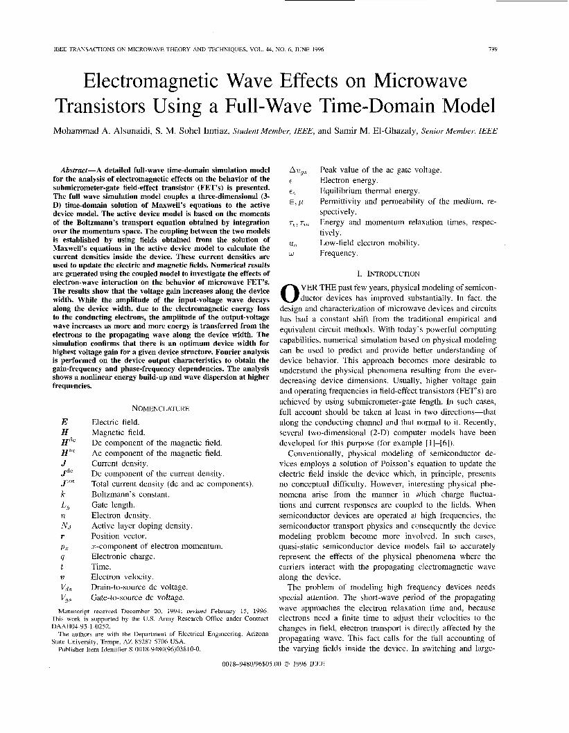
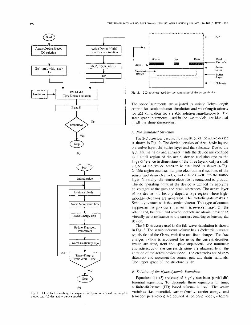
Equations (1 1) and (12) give the electric and magnetic field distributions at each time step. These new values are used by the semiconductor model to update the current density at the same time step. These current densities ,are fed back to the Maxwell’s equations again to calculate the electric and magnetic fields in the following time step. This process of updating the fields and the current densities progresses in time in response to applied excitation and moves on for an appreciable amount of time to study the device behavior. The flowchart in Fig. l(a) outlines the calculkition steps and the coupling procedure between the semiconductor and the electromagnetic models. The flowchart in Fig. 1 (b) describes the sequence of operations in the active device model.
111. IMPLEMENTATION USING FDTD METHOD
Both finite-difference and finite-element schemes were used in semiconductor device simulations. Although the finite- element method provides a flexible way of solving com- plex geometries and requires fewer nodes than the finite difference scheme, it requires a matnix reordering algorithm to deal with the generated complex matrix structure. This process reduces the speed of the solution. The finite-difference method, on the other hand, lends itself naturally to the simple rectangular geometry generally considered for semiconductor device simulations. Also, finite-difference schemes are easier to formulate and considerable information is available on their stability and convergence properties [l4]. In this work, several finite-difference techniques, such as the upwind and the Lax methods, are used in conjunction with the basic finite- difference formulation to achieve stable and accurate solutions.
802 IEEE TRANSACTIONS ON MICROWAVE THEORY AND TECHNIQUES, VOL. 44, NO. 6, JUNE 1996
r-------- - - - - - - - - - - - - - - - - - - - - - - - - -I- I
1 I I I I I I I I
I I I I I I I I
I Air
r= I Time Domain solution
Y i Source Gate Drain I Metal Electrode
-Active Layer
Buffer Layer - Substrate
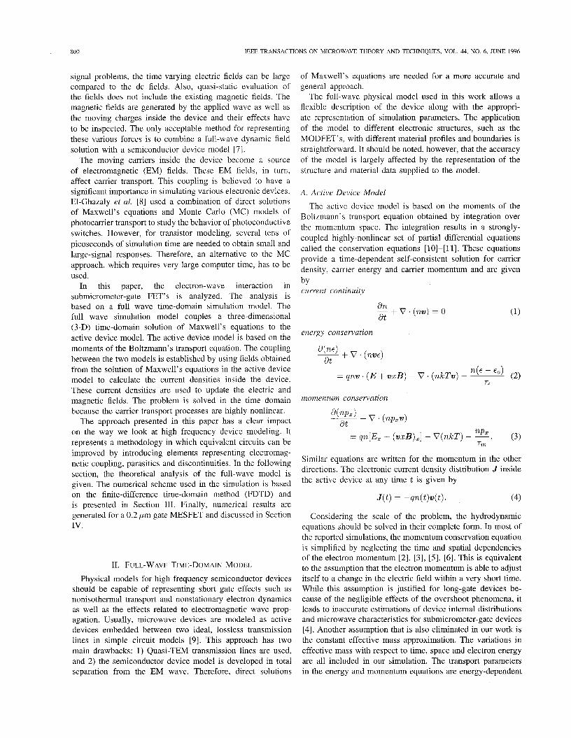
Fig. 2. 2-D structure used for the simulation of the active device. Time Domain solution
The space increments are adjusted to satisfy Debye length criteria for semiconductor simulation and wavelength criteria for EM simulation for a stable solution simultaneously. The same space increments, used in the two models, are identical in all the three dimensions.
A. The Simulated Structure
The 2-D structure used in the simulation of the active device is shown in Fig. 2. The device consists of three basic layers: the active layer, the buffer layer and the substrate. Due to the fact that the fields and currents inside the device are confined to a small region of the actual device and also due to the large difference in dimensions of the three layers, only a small region of the device needs to be simulated as shown in Fig. 2. This region encloses the gate electrode and sections of the source and drain electrodes, and extends well into the buffer layer. Normally, the source electrode is connected to ground. The dc operating point of the device is defined by applying dc voltages at the gate and drain electrodes. The active layer of the device is a heavily doped n-type region where high- mobility electrons are generated. The metallic gate makes a Schottky contact with the semiconductor. This type of contact suppresses the gate current when it is reverse biased. On the other hand, the drain and source contacts are ohmic, presenting virtually zero resistance to the carriers entering or leaving the device.
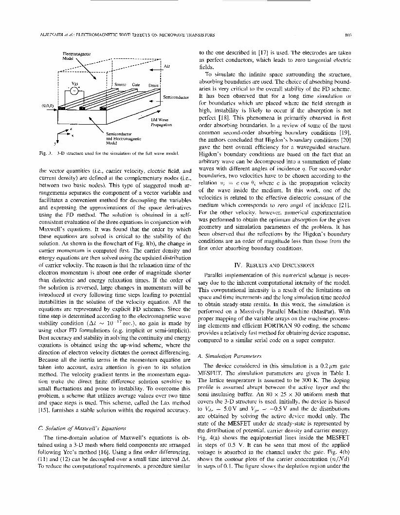
The 3-D structure used in the full-wave simulation is shown in Fig. 3. The semiconductor volume has a dielectric constant equals that of the GaAs, with free and fixed charges. The free charges motion is accounted for using the current densities which are time, field and space dependent. The nonlinear characteristics of the current densities are obtained from the solution of the active device model. The electrodes are of zero thickness and represent the source, gate and drain terminals. The upper space of the structure is air.
B. Solution of the Hydrodynamic Equations
Equations (1)-(3) are coupled highly nonlinear partial dif- ferential equations. To decouple these equations in time, a finite-difference (FD) based scheme is used. The scalar
transport parameters) are defined at the basic nodes, whereas
(b)
model and (b) the active device model. Fig. 1. Flowchart describing the sequence of operations in (a) the coupled (i.e., potential, carrier density, carrier energy, and
ALSUNAIDI et al.: ELECTROMAGNETIC WAVE EFFECTS ON MICROWAVE TRANSISTORS
~
803
Electromagnetic
! ! I
‘ Semiconductor and Electromagnetic
Y Model
Fig. 3. 3-D structure used for the simulation of the full-wave model.
the vector quantities (i.e., carrier velocity, electric field, and current density) are defined at the complementary nodes (Le., between two basic nodes). This type of staggered mesh ar- rangements separates the component of a vector variable and facilitates a convenient method for decoupling the variables and expressing the approximations of the space derivatives using the FD method. The solution is obtained in a self- consistent evaluation of the three equations in conjunction with Maxwell’s equations. It was found that the order by which these equations are solved is critical to the stability of the solution. As shown in the flowchart of Fig. l(b), the change in carrier momentum is computed first. The carrier density and energy equations are then solved using the updated distribution of carrier velocity. The reason is that the relaxation time of the electron momentum is about one order of magnitude shorter than dielectric and energy relaxation times. If the order of the solution is reversed, large changes in momentum will be introduced at every following time steps leading to potential instabilities in the solution of the velocity equation. All the equations are represented by explicit FD schemes. Since the time step is determined according to the electromagnetic wave stability condition (At N 10-17sec.), no gain is made by using other FD formulations (e.g. implicit or semi-implicit). Best accuracy and stability in solving the continuity and energy equations is obtained using the up-wind scheme, where the direction of electron velocity dictates the correct differencing. Because all the inertia terms in the momentum equation are taken into account, extra attention is given to its solution method. The velocity gradient terms in the momentum equa- tion make the direct finite difference solution sensitive to small fluctuations and prone to instability. To overcome this problem, a scheme that utilizes average values over two time and space steps is used. This scheme, called the Lax method [ 151, furnishes a stable solution within the required accuracy.
C. Solution of Maxwell’s Equations
The time-domain solution of Maxwell’s equations is ob- tained using a 3-D mesh where field components are arranged following Yee’s method [16]. Using a first order differencing, (11) and (12) can be decoupled over a small time interval At. To reduce the computational requirements, a procedure similar
to the one described in [17] is used. The electrodes are taken as perfect conductors, which leads to zero tangential electric fields.
To simulate the infinite space surrounding the structure, absorbing boundaries are used. The choice of absorbing bound- aries is very critical to the overall stability of the FD scheme. It has been observed that for a long time simulation or for boundaries which are placed where the field strength is high, instability is likely to occur if the absorption is not perfect [18]. This phenomena is primarily observed in first order absorbing boundaries. In a review of some of the most common second-order absorbing boundary conditions [ 191, the authors concluded that Higdon’s boundary conditions [20] gave the best overall efficiency for a waveguided structure. Higdon’s boundary conditions are based on the fact that an arbitrary wave can be decomposed into a summation of plane waves with different angles of incidence q . For second-order boundaries, two velocities have to be chosen according to the relation TI, = c cos 0, where c is the propagation velocity of the wave inside the medium. In this work, one of the velocities is related to the effective dielectric constant of the medium which corresponds to zero angel of incidence [21]. For the other velocity, however. numerical experimentation was performed to obtain the optimum absorption for the given geometry and simulation parameters of the problem. It has been observed that the reflections by the Higdon’s boundary conditions are an order of magnitude less than those from the first order absorbing boundary conditions.
Iv. RESULTS AND DISCUSSIONS
Parallel implementation of this numerical scheme is neces- sary due to the inherent computational intensity of the model. This computational intensity is a result of the limitations on space and time increments and the long simulation time needed to obtain steady-state results. In this work, the simulation is performed on a Massively Parallel Mrachine (MasPar). With proper mapping of the variable arrays on the machine process- ing elements and efficient FORTRAN 90 coding, the scheme provides a relatively fast method for obtaining device response, compared to a similar serial code on a super computer.
A. Simulation Parameters
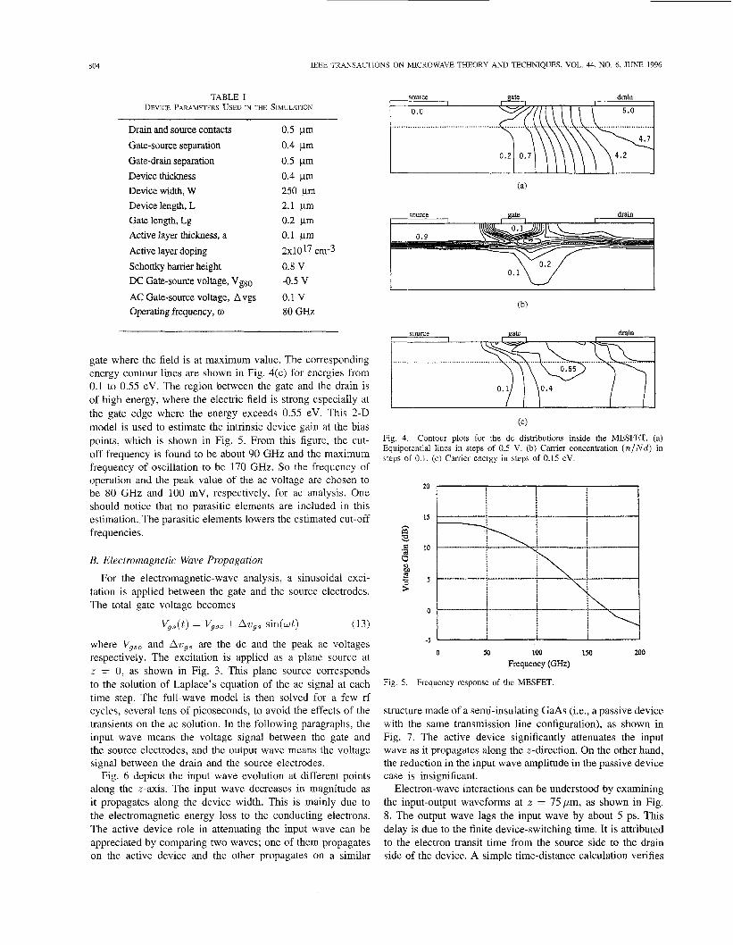
The device considered in this simulation is a 0.2pm gate MESFET. The simulation parameters are given in Table I. The lattice temperature is assumed to be 300 K. The doping profile is assumed abrupt between thie active layer and the semi-insulating buffer. An 80 x 25 x 30 uniform mesh that covers the 3-D structure is used. Initially, the device is biased to V& = 5.0 V and V,, = -0.5 V and the dc distributions are obtained by solving the active device model only. The state of the MESFET under dc steady-state is represented by the distribution of potential, carrier density and carrier energy. Fig. 4(a) shows the equipotential lines inside the MESFET in steps of 0.5 V. It can be seen that most of the applied voltage is absorbed in the channel under the gate. Fig. 4(b) shows the contour plots of the carrier concentration (n /Nd) in steps of 0.1. The figure shows the depletion region under the
804 JEEE TRANSACTIONS ON MICROWAVE THEORY AND TECHNIQUES, VOL. 44, NO. 6, JUNE 1996
TABLE I source drain I
0.0 DEVICE PARAMETERS USED IN THE SIMULATION
............................................... Drain and source contacts 0.5 pm Gate-source separation 0.4 pm Gate-drain separation 0.5 prn Device thickness 0.4 Km Device width, W 250 prn (a)
Device length, L Gate length, Lg Active layer thickness, a Active layer doping Schottky barrier height DC Gate-source voltage, Vgso AC Gate-source voltage, Avgs Operating frequency, w
2.1 pm 0.2 pm 0.1 pm 2x1017 cm-3 0.8 V -0.5 V 0.1 v 80 GHz
gate where the field is at maximum value. The corresponding energy contour lines are shown in Fig. 4(c) for energies from 0.1 to 0.55 eV. The region between the gate and the drain is of high energy, where the electric field is strong especially at the gate edge where the energy exceeds 0.55 eV. This 2-D model is used to estimate the intrinsic device gain at the bias points, which is shown in Fig. 5. From this figure, the cut- off frequency is found to be about 90 GHz and the maximum frequency of oscillation to be 170 GHz. So the frequency of operation and the peak value of the ac voltage are chosen to be 80 GHz and 100 mV, respectively, for ac analysis. One should notice that no parasitic elements are included in this estimation. The parasitic elements lowers the estimated cut-off frequencies.
B. Electromagnetic Wave Propagation
For the electromagnetic-wave analysis, a sinusoidal exci- tation is applied between the gate and the source electrodes. The total gate voltage becomes
(13)
where V,,, and Avgs are the dc and the peak ac voltages respectively. The excitation is applied as a plane source at z = 0, as shown in Fig. 3. This plane source corresponds to the solution of Laplace’s equation of the ac signal at each time step. The full-wave model is then solved for a few rf cycles, several tens of picoseconds, to avoid the effects of the transients on the ac solution. In the following paragraphs, the input wave means the voltage signal between the gate and the source electrodes, and the output wave means the voltage signal between the drain and the source electrodes.
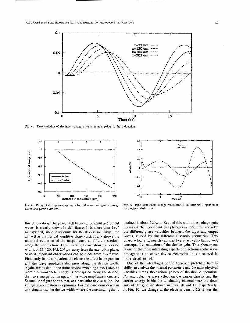
Fig. 6 depicts the input wave evolution at different points along the z-axis. The input wave decreases in magnitude as it propagates along the device width. This is mainly due to the electromagnetic energy loss to the conducting electrons. The active device role in attenuating the input wave can be appreciated by comparing two waves; one of them propagates on the active device and the other propagates on a similar
V,,(t) = V,,, + Avgs sin(wt)
source drain
source
(c)
Fig. 4. Contour plots for the dc distributions inside the MESFET. (a) Equipotential lines in steps of 0.5 V. (b) Carrier concentration ( n / N d ) in steps of 0.1. (c) Carrier energy in steps of 0.15 eV.
0 50 100 150 Frequency (GHz)
Fig. 5. Frequency response of the MESFET.
structure made of a semi-insulating GaAs (i.e., a passive device with the same transmission line configuration), as shown in Fig. 7. The active device significantly attenuates the input wave as it propagates along the z-direction. On the other hand, the reduction in the input wave amplitude in the passive device case is insignificant.
Electron-wave interactions can be understood by examining the input-output waveforms at z = 75pm, as shown in Fig. 8. The output wave lags the input wave by about 5 ps. This delay is due to the finite device-switching time. It is attributed to the electron transit time from the source side to the drain side of the device. A simple time-distance calculation verifies
ALSUNAIDI ef al.: ELECTROMAGNETIC WAVE EFFECTS ON MICROWAVE TRANSISTORS 805
0.1 1 1 1
2=75um - 2=120um ---. 2=165 u m - - - - ~ 2 0 5 um ....--..
-0.05 -
-0.1 I 1 I
0 5 10 15 Time (ps)
Fig. 6. Time variation of the input-voltage wave at several points in the z-direction.
1 -
0.9 -
0.8 -
0.7 -
0.6 -
0.5 I I I I I
0 50 100 150 200 250 Distance in z-direction (um)
Fig. 7. Decay of the input-voltage wave for EM wave propagation through active and passive devices.
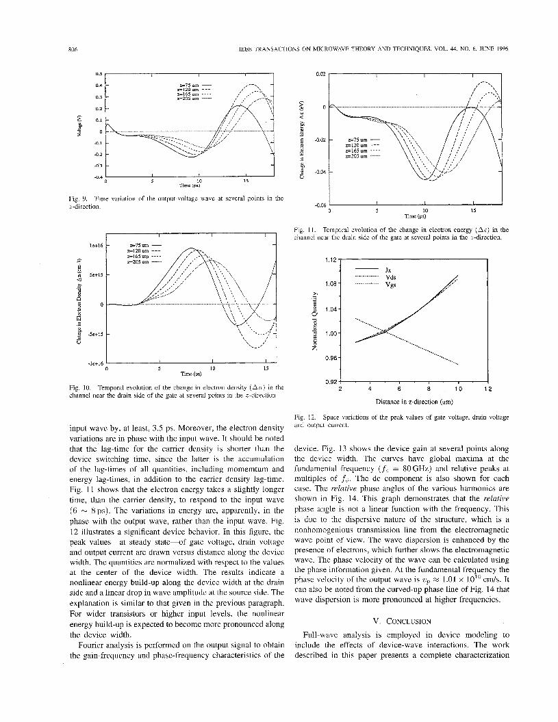
this observation. The phase shift between the input and output waves is clearly shown in this figure. It is more than 180' as expected, since it accounts for the device switching time as well as the normal amplifier phase shift. Fig. 9 shows the temporal evolution of the output wave at different sections along the z direction. These variations are shown at device widths of 75, 120, 165,205 pm away from the excitation plane. Several important observations can be made from this figure. First, early in the simulation, the electronic effect is not present and the wave amplitude decreases along the device width. Again, this is due to the finite device switching time. Later, as more electromagnetic energy is propagated along the device, the wave energy builds up, and the wave amplitude increases. Second, the figure shows that, at a particular device width, the voltage amplification is optimum. For the case considered in this simulation, the device width where the maximum gain is
10 15 l ime (pa)
Input- and output-voltage waveforms of the MESFET. InDut: solid line, output: dashed line.
-
attained is about 120 pm. Beyond this width, the voltage gain decreases. To understand this phenomena, one must consider the different phase velocities between the input and output waves, caused by the different electrode geometries. This phase velocity mismatch can lead to a phase cancellation and, consequently, reduction of the device gain. This phenomena is one of the most interesting aspects of electromagnetic wave propagations on active device electrodes. It is discussed in more detail in [9].
One of the advantages of the approach presented here is ability to analyze the internal parameters and the main physical variables during the various phases of the device operation. For example, the wave effect on the carrier density and the carrier energy inside the conducting channel near the drain side of the gate are shown in Figs. 10 and 11, respectively. In Fig. 10, the change in the electron density (An) lags the
806
.- x 1.0,:
1.04- 6 Ti 4 1.00- E z
0.96 -
0.92
IEEE TRANSACTIONS ON MICROWAVE THEORY AND TECHNIQUES, VOL. 44, NO. 6, JUNE 1996
./. -
-.. *... ..-*:..
.%. %. ---_ .... .-._ *..
+%. .-. ..
0.02 I I 1 I
6.4 oo 10 15
Time (pn)
Fig. 9. z-direction.
Time variation of the output-voltage wave at several points in the
le+16
5e+15
0
-5e+15
-le+16 1 0 5 10 15
Time (ps)
Temporal evolution o f the change in electron density (An) in the Fig. 10. channel near the drain side of the gate at several points in the z-direction.
input wave by, at least, 3.5 ps. Moreover, the electron density variations are in phase with the input wave. It should be noted that the lag-time for the carrier density is shorter than the device switching time, since the latter is the accumulation of the lag-times of all quantities, including momemtum and energy lag-times, in addition to the camer density lag-time. Fig. 11 shows that the electron energy takes a slightly longer time, than the carrier density, to respond to the input wave (6 N 8 ps). The variations in energy are, apparently, in the phase with the output wave, rather than the input wave. Fig. 12 illustrates a significant device behavior. In this figure, the peak values-at steady state-of gate voltage, drain voltage and output current are drawn versus distance along the device width. The quantities are normalized with respect to the values at the center of the device width. The results indicate a nonlinear energy build-up along the device width at the drain side and a linear drop in wave amplitude at the source side. The explanation is similar to that given in the previous paragraph. For wider transistors or higher input levels, the nonlinear energy build-up is expected to become more pronounced along the device width.
Fourier analysis is performed on the output signal to obtain the gain-frequency and phase-frequency characteristics of the
-0.06 I I I 1
0 5 10 15 Time (ps)
Fig. 11. channel near the drain side of the gate at several points in the z-direction.
Temporal evolution of the change in electron energy (At) in the
1.12 ,
2
Distance in z-direction (um)
Space variations o f the peak values of gate voltage, drain voltage Fig. 12. and output current.
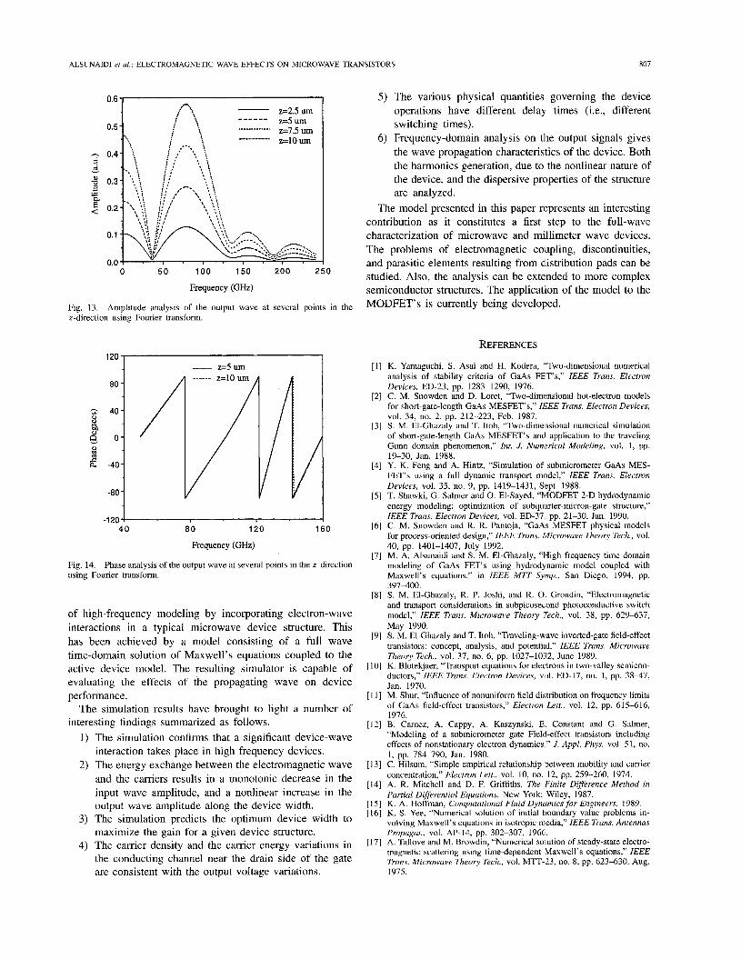
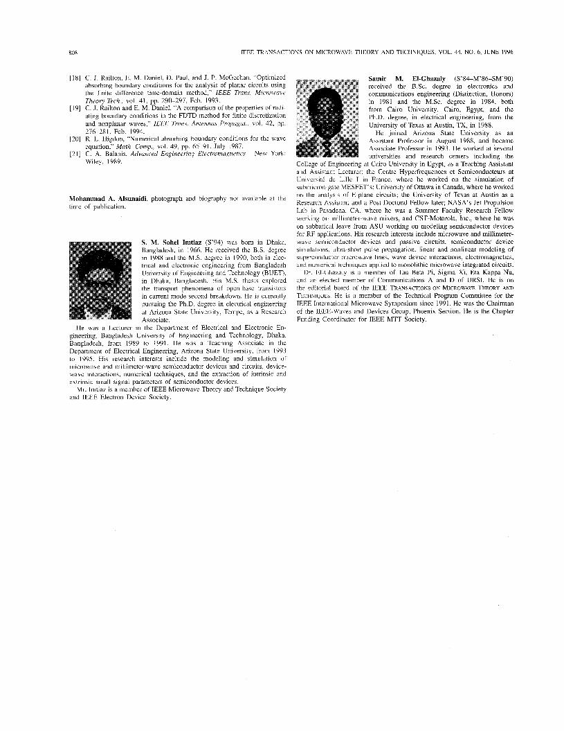
device. Fig. 13 shows the device gain at several points along the device width. The curves have global maxima at the fundamental frequency ( f o = 80 GHz) and relative peaks at multiples of f o . The dc component is also shown for each case. The relative phase angles of the various harmonics are shown in Fig. 14. This graph demonstrates that the relative phase angle is not a linear function with the frequency. This is due to the dispersive nature of the structure, which is a nonhomogenious transmission line from the electromagnetic wave point of view. The wave dispersion is enhanced by the presence of electrons, which further slows the electromagnetic wave. The phase velocity of the wave can be calculated using the phase information given. At the fundamental frequency the phase velocity of the output wave is 'up M 1.01 x lo1' c d s . It can also be noted from the curved-up phase line of Fig. 14 that wave dispersion is more pronounced at higher frequencies.
V. CONCLUSION
Full-wave analysis is employed in device modeling to include the effects of device-wave interactions. The work described in this paper presents a complete characterization
ALSUNAIDI et al.: ELECTROMAGNETIC WAVE EFFECTS ON MICROWAVE TRANSISTORS 807
80 -
3 40- E 8 e 0-
!4 e -40-
-80 -
z=2.5 um z=5 um z=7.5 um z=10 um
------ p! I . : . : % , . . . .. . . __. -. ,
-- 0.5 -
0 50 100 150 200 250
Frequency (GHz)
Fig. 13. z-direction using Fourier transform.
Amplitude analysis of the output wave at several points in the
5 ) The various physical quantities governing the device operations have different delay times (i.e., different switching times).
6) Frequency-domain analysis on the output signals gives the wave propagation characteristics of the device. Both the harmonics generation, due to the nonlinear nature of the device, and the dispersive properties of the structure are analyzed.
The model presented in this paper represents an interesting contribution as it constitutes a first step to the full-wave characterization of microwave and millimeter wave devices. The problems of electromagnetic coupling, discontinuities, and parasitic elements resulting from distribution pads can be studied. Also, the analysis can be extended to more complex semiconductor structures. The application of the model to the MODFET’s is currently being developed.
REFERENCES
I‘=” 1 - z=5um
-1204 4 0 80 120 160
Frequency (GHz)
Fig. 14. using Fourier transform.
Phase analysis of the output wave at several points in the z-direction
of high-frequency modeling by incorporating electron-wave interactions in a typical microwave device structure. This has been achieved by a model consisting of a full wave time-domain solution of Maxwell’s equations coupled to the active device model. The resulting simulator is capable of evaluating the effects of the propagating wave on device performance.
The simulation results have brought to light a number of interesting findings summarized as follows.
The simulation confirms that a significant device-wave interaction takes place in high frequency devices. The energy exchange between the electromagnetic wave and the carriers results in a monotonic decrease in the input wave amplitude, and a nonlinear increase in the output wave amplitude along the device width. The simulation predicts the optimum device width to maximize the gain for a given device structure. The carrier density and the carrier energy variations in the conducting channel near the drain side of the gate are consistent with the output voltage variations.
K. Yamaguchi, S. Asai and H. Kodera, “Two-dimensional numerical analysis of stability criteria of GaAs FET’s,” IEEE Trans. Electron Devices, ED-23, pp. 1283-1290, 1976. C. M. Snowden and D. Loret, “Two-dimensional hot-electron models for short-gate-length GaAs MESFET’s,” IEEE Trans. Electron Devices, vol. 34, no. 2, pp. 212-223, Feb. 1987. S. M. El-Ghazaly and T. Itoh, “Two-dimensional numerical simulation of short-gate-length GaAs MESFET’s and application to the traveling Gunn domain phenomenon,” Int. .I. Numerical Modeling, vol. 1, pp. 19-30, Jan. 1988. Y. K. Feng and A. Hintz, “Simulation of submicrometer GaAs MES- FET’s using a full dynamic transport model,” IEEE Trans. Electron Devices, vol. 35, no. 9, pp. 1419-1431, Sept. 1988. T. Shawki, G. Salmer and 0. El-Sayed, “h4ODFET 2-D hydrodynamic energy modeling: optimization of subquarter-micron-gate structure,” IEEE Trans. Electron Devices, vol. ED-37, pp. 21-30, Jan. 1990. C. M. Snowden and R. R. Pantoja, “GaAs MESFET physical models for process-oriented design,” IEEE Trans. Microwave Theory Tech., vol. 40, pp. 1401-1407, July 1992. M. A. Alsunaidi and S. M. El-Ghazaly, “High frequency time domain modeling of GaAs FET’s using hydrodynamic model coupled with Maxwell’s equations,” in IEEE MTT Symp., San Diego, 1994, pp. 397400. S. M. El-Ghazaly, R. P. Joshi, and R. 0. Grondin, “Electromagnetic and transport considerations in subpicosecond photoconductive switch model,” IEEE Trans. Microwave Theory Tech., vol. 38, pp. 629-637, May 1990. S. M. El-Ghazaly and T. Itoh, “Traveling-wave inverted-gate field-effect transistors: concept, analysis, and potential,” IEEE Trans. Microwave Theory Tech., vol. 37, no. 6, pp. 1027-1032, June 1989. K. Blotekjaer, “Transport equations for electrons in two-valley semicon- ductors,” IEEE Trans. Electron Devices, VOI. ED-17, no. 1, pp. 3 8 4 7 , Jan. 1970. M. Shur, “Influence of nonuniform field distribution on frequency limits of GaAs field-effect transistors,” Electron Letr., vol. 12, pp. 615-616, 1976. B. Camez, A. Cappy, A. Kaszynski, E. Constant and G. Salmer, “Modeling of a submicrometer gate Field-effect transistors including effects of nonstationary electron dynamics,” .I. Appl. Phys. vol. 5 1, no. 1, pp. 784-790, Jan. 1980. C. Hilsum, “Simple empirical relationship between mobility and carrier concentration,” Electron Lett., vol. 10, no. 12, pp. 259-260, 1974. A. R. Mitchell and D. F. Griffiths, The Finite Difference Method in Partial Differential Equations. New York Wiley, 1987. K. A. Hoffman, Computational Fluid Dynamics for Engineers. 1989. K. S. Yee, “Numerical solution of initial boundary value problems in- volving Maxwell’s equations in isotropic media,” IEEE Trans. Antennas Propagat., vol. AP-14, pp. 302-307, 19668. A. Taflove and M. Browdin, “Numerical solution of steady-state electro- magnetic scattering using time-dependent Maxwell’s equations,” IEEE Trans. Microwave Theory Tech., vol. MTT-23, no. 8, pp. 623-630, Aug. 1975.
808 IEEE TRANSACTIONS ON MICROWAVE THEORY AND TECHNIQUES, VOL. 44, NO. 6, JUNE 1996
[18] C. J. Railton, E. M. Daniel, D. Paul, and J. P. McGeehan, “Optimized absorbing boundary conditions for the analysis of planar circuits using the finite difference time-domain method,” IEEE Trans. Microwave Theory Tech., vol. 41, pp. 290-297, Feb. 1993.
[19] C. J. Railton and E. M. Daniel, “A comparison of the properties of radi- ating boundary conditions in the FDTD method for finite discretization and nonplanar waves,” IEEE Trans. Antennas Propagat., vol. 42, pp. 276-281, Feb. 1994.
1201 R. L. Higdon, “Numerical absorbing boundary conditions for the wave equation,” Math. Comp., vol. 49, pp. 65-91, July 1987.
[21] C. A. Balanis, Advanced Engineering Electromagnetics. New York: Wiley, 1989.
Mohammad A. Alsunaidi, photograph and biography not available at the time of publication.
S. M. Sohel Imtiaz (S’94) was born in Dhaka. Bangladesh, in 1966. He received the B.S. degree in 1988 and the M.S. degree in 1990, both in elec- trical and electronic engineering from Bangladesh University of Engineering and Technology (BUET), in Dhaka, Bangladesh. His M.S. thesis explored the transport phenomena of open-base transistors in current mode second breakdown. He is currently pursuing the Ph.D. degree in electrical engineering at Arizona State University, Tempe, as a Research Associate.
He was a Lecturer in the Department of Electrical and Electronic En- gineering, Bangladesh University of Engineering and Technology, Dhaka. Bangladesh, from 1989 to 1991. He was a Teaching Associate in the Department of Electrical Engineering, Arizona State University, from 1993 to 1995. His research interests include the modeling and simulation of microwave and millimeter-wave semiconductor devices and circuits, device- wave interactions, numerical techniques, and the extraction of intrinsic and extrinsic small signal parameters of semiconductor devices.
Mr. Imtiaz is a member of IEEE Microwave Theory and Technique Society and IEEE Electron Device Society.
Samir M. El-Ghazaly (S’84-M’86-SM’90) received the B.Sc. degree in electronics and communications engineering (Distinction, Honors) in 1981 and the M.Sc. degree in 1984, both from Cairo University, Cairo, Egypt, and the Ph.D. degree, in electrical engineering, from the University of Texas at Austin, TX, in 1988.
He joined Arizona State University as an Assistant Professor in August 1988, and became Associate Professor in 1993. He worked at several universities and research centers including the
I
College of Engineering at Cairo University in Egypt, as a Teaching Assistant and Assistant Lecturer; the Centre Hyperfrequences et Semiconducteurs at Universitt de Lille I in France, where he worked on the simulation of submicron-gate MESFET’s; University of Ottawa in Canada, where he worked on the analysis of E-plane circuits; the University of Texas at Austin as a Research Assistant and a Post Doctoral Fellow later; NASA’s Jet Propulsion Lab in Pasadena, CA, where he was a Summer Faculty Research Fellow working on millimeter-wave mixers, and CST-Motorola, Inc., where he was on sabbatical leave from ASU working on modeling semiconductor devices for RF applications. His research interests include microwave and millimeter- wave semiconductor devices and passive circuits, semiconductor device simulations, ultra-short pulse propagation, linear and nonlinear modeling of superconductor microwave lines, wave-device interactions, electromagnetics, and numerical techniques applied to monolithic microwave integrated circuits.
Dr. El-Ghazaly is a member of Tau Beta Pi, Sigma Xi, Eta Kappa Nu, and an elected member of Communications A and D of URSI. He is on the editorial hoard of the IEEE TRANSACTIONS ON MICROWAVE THEORY AND
TECHNIQUES He is a member of the Technical Program Committee for the IEEE International Microwave Symposium since 1991. He was the Chairman of the IEEE-Waves and Devices Group, Phoenix Section. He is the Chapter Funding Coordinator for IEEE MTT Society.