electromagnetic modeling of gan varactor microwave switches
TRANSCRIPT

University of South Carolina University of South Carolina
Scholar Commons Scholar Commons
Theses and Dissertations
1-1-2013
Electromagnetic Modeling of GaN Varactor Microwave Switches Electromagnetic Modeling of GaN Varactor Microwave Switches
YI-HSUAN YANG University of South Carolina
Follow this and additional works at: https://scholarcommons.sc.edu/etd
Part of the Electrical and Electronics Commons
Recommended Citation Recommended Citation YANG, Y.(2013). Electromagnetic Modeling of GaN Varactor Microwave Switches. (Master's thesis). Retrieved from https://scholarcommons.sc.edu/etd/2416
This Open Access Thesis is brought to you by Scholar Commons. It has been accepted for inclusion in Theses and Dissertations by an authorized administrator of Scholar Commons. For more information, please contact [email protected].

Electromagnetic Modeling of GaN Varactor Microwave Switches
by
Yi-Hsuan Yang
Bachelor of Engineering
Ming Chuan University, Taiwan, 2006
Submitted in Partial Fulfillment of the Requirements
For the Degree of Master of Science in
Electrical Engineering
College of Engineering and Computing
University of South Carolina
2013
Accepted by:
Grigory Simin, Director of Thesis
Guoan Wang, Reader
Lacy Ford, Vice Provost and Dean of Graduate Studies

ii
© Copyright by Yi-Hsuan Yang, 2013
All Rights Reserved

iii
ACKNOWLEDGEMENTS
First and foremost, I would like to express my gratitude to my advisor Dr. Grigory Simin
for giving me this good opportunity to do research under his supervision. I am grateful to
him for his guidance, support and encouragement throughout my master’s program.
Without his help, I could have never been where I am.
I am also grateful to my thesis committee member, Dr. Guoan Wang for providing many
helpful suggestions about my research.
I would like to thank all my past and current colleagues in the Microwave
Microelectronics research group. I would specially like to thank Faisal Jahan for his
constant support, suggestion and discussion throughout this work which has greatly
helped me to achieve my goals.
Last, but not least, I would like to thank my family and my friends for their love, support
and encouragement.

iv
ABSTRACT
Microwave switches are important components which have been widely used in
many microwave systems, such as electronic products, satellites communications,
antennas, and radars etc. Traditionally, microwave switches are fabricated using pin
diodes or MEMS, Si MOSFETs or GaAs HEMTs. These devices, due to the material
limitations are suffering from a low breakdown voltage and are unable to handle high
power. III-Nitride based varactor microwave switches provide opportunities for high
power microwave devices, due to highly conducting 2D electron gas in the channel and
high breakdown electric field.
Designing microwave switches typically involves modeling and simulation using
tools such as MATLAB, ADS etc, to save the designing time and cost. However, these
tools are not sufficient for precise simulation of low-loss microwave switches, where
even minor scattering and loss in waveguides incorporating the device, may have
significant effect on the overall switch performance.
In this thesis, HFSS electromagnetic simulation method is introduced to simulate
microwave switches using GaN HFETs and varactors. First, the HFET and varactor
models for HFSS has been developed and validated. Then various types of microwave
switches with operating frequency above 10GHz have been simulated and optimized.
Specific emphasis is made on a novel capacitively coupled contacts (C3) varactor, not
requiring ohmic contacts and gate electrodes. Using HFSS, this thesis demonstrated

v
several modified C3 switch structures, achieving resonance in the operating frequency
range thus greatly increasing the isolation, up to 42dB at 22GHz.

vi
TABLE OF CONTENTS
Acknowledgements ............................................................................................................ iii
Abstract .............................................................................................................................. iv
List of Tables ................................................................................................................... viii
List of Figures .................................................................................................................... ix
CHAPTER 1 Introduction ................................................................................................... 1
1.1 Microwave Switches and Applications ................................................................... 1
1.2 Key Parameters for Microwave Switch .................................................................. 5
1.3 GaN HFET and C3 Varactor .................................................................................. 6
1.4 Electromagnetic Software ..................................................................................... 10
1.5 Outline of This Thesis ........................................................................................... 12
CHAPTER 2 Problem Identification ................................................................................ 14
2.1 Problem Identification .......................................................................................... 14
CHAPTER 3 HFSS simulation of HFET Microwave Switches ....................................... 17
3.1 Introduction ........................................................................................................... 17
3.2 Through ................................................................................................................. 19
3.3 Series Structure (100um) ...................................................................................... 21
3.4 HFET Single Pole Single Throw(SPST) Switch .................................................. 23
CHAPTER 4 HFSS simulation of GaN Varactor Switches .............................................. 27
4.1 Introduction ........................................................................................................... 27

vii
4.2 C3
Varactor Test Structure Design & Simulation ................................................ 30
4.3 C3 Single Pole Single Throw(SPST) Switch (0.5mm/0.5mm) ............................. 33
4.4 C3 Single Pole Double Throw(SPDT) Switch ...................................................... 40
CHAPTER 5 Conclusion and Future work ....................................................................... 47
5.1 Conclusion ............................................................................................................ 47
5.2 Future work ........................................................................................................... 49
References ......................................................................................................................... 50

viii
LIST OF TABLES
Table 1.1: the comparison of different parameters in electromechanical and
solid state switches[5] ......................................................................................................... 4
Table 1.2: the comparison of different switch technologies [4] ......................................... 5
Table 1.3:the comparison of major electronic properties of GaN
to other semiconductors [7] ................................................................................................ 7
Table 1.4: Common EDA simulation software in the market [15][16] ............................ 11
Table 3.1 Material parameter for HFET switch in HFSS ................................................. 22
Table 5.1 Comparison of three different works with improved switch performance ....... 49

ix
LIST OF FIGURES
Figure 1.1 Different applications of microwave switches .................................................. 1
Figure 1.2 The schematic of a HFET structure ................................................................... 8
Figure 1.3 The schematic of a C3 structure ......................................................................... 9
Figure 1.4 FEM three-dimensional mesh [18] .................................................................. 12
Figure 2.1 The comparison results of insertion loss ......................................................... 15
Figure 3.1 A HFET microwave switch ............................................................................. 18
Figure 3.2 The mesh generation of a HFSS through model ............................................. 19
Figure 3.3 HFSS Diagram of through structure ................................................................ 20
Figure 3.4 Through structure shows around 0dB insertion loss ....................................... 20
Figure 3.5 HFSS Series structure diagram ........................................................................ 21
Figure 3.6 HFSS model design for HFET ON/OFF state ................................................. 22
Figure 3.7 Insertion loss and Isolation of series structure ................................................ 23
Figure 3.8 HFSS-SPST 1.05mm/0.75mm structure diagram ........................................... 24
Figure 3.9 Insertion loss and Isolation of HFET-SPST 1.05mm/0.75mm switch ............ 25
Figure 3.10 HFSS-SPST 0.4mm/0.4mm structure diagram ............................................. 26
Figure 3.11 Insertion loss and Isolation of HFET-SPST 0.4mm/0.4mm switch .............. 26
Figure 4.1 Comparison structure of ohmic and C3
contact ............................................... 28
Figure 4.2 The schematic of C3
varactor ........................................................................... 29
Figure 4.3 HFSS model design for C3
device ON/OFF state ............................................ 31

x
Figure 4.4 C3
series 250um structure diagram .................................................................. 32
Figure 4.5 Insertion loss and Isolation of C3
Series structures.......................................... 33
Figure 4.6 Series-shunt MMIC layout .............................................................................. 34
Figure 4.7 Equivalent circuit in ON and OFF states ......................................................... 34
Figure 4.8 Simulated Insertion loss and Isolation over varying frequency with and
without added inductance from MATLAB ....................................................................... 35
Figure 4.9 Insertion loss and Isolation of real C3
SPST switch ........................................ 36
Figure 4.10 C3
SPST 0.5mm/0.5mm structure diagram .................................................... 36
Figure 4.11 Insertion loss and Isolation of C3
SPST 0.5mm/0.5mm switch ..................... 37
Figure 4.12 C3
SPST 0.5mm/0.5mm structure diagram with smooth corner.................... 38
Figure 4.13 Comparison of insertion loss and isolation of C3 SPST 0.5mm/0.5mm switch
with/without smooth corner .............................................................................................. 38
Figure 4.14 Modified C3
SPST 0.5mm/0.5mm structure diagram .................................... 39
Figure 4.15 Insertion loss and Isolation of modified C3 SPST 0.5mm/0.5mm switch ..... 40
Figure 4.16 C3
SPDT 0.25mm/0.2mm structure diagram ................................................. 41
Figure 4.17 Insertion loss and Isolation of C3 SPDT 0.25mm/0.2mm switch .................. 42
Figure 4.18 C3
Modified SPDT 0.25mm/0.2mm structure diagram ................................. 44
Figure 4.19 Insertion loss and Isolation of C3 SPDT modified switch ............................. 45
Figure 4.20 New C3
SPDT design structure diagram........................................................ 46
Figure 4.21 Insertion loss and Isolation of C3 SPDT design switch ................................. 46

1
CHAPTER 1 INTRODUCTION
1.1 MICROWAVE SWITCHES AND APPLICATIONS
Microwave switches, with an electromagnetic spectrum of 300MHz to 30GHz,
are components which have been widely used in many microwave systems, such as
electronic products, satellites communications, antennas, radars and so on, as shown in
the Figure 1.1[1]. These applications make microwave switches become one of the most
important components in RF circuits and wireless communication systems.
(a) 3G cellular multimode devices (b) Radar
(c) Satellite (d) Radar Antennas
Figure 1.1 Different applications of microwave switches

2
Microwave switches can be classified into two main categories:
electromechanical switches and solid state switches. The operating principle of
electromechanical switches is simply mechanically switching the cantilever or membrane
up and down to the contact pad by the theory of electromagnetic induction. So during the
switching process, the contact pad of switch changes its position physically. For
applications require high power or lowest possible loss, electromechanical switches are
usually used. Solid state switches, like PIN diode, MESFETs (Metal Semiconductor Field
Effect Transistor), HEMTs (High Electron Mobility Transistor), HFETs (Heterostructure
Field Effect Transistor), CMOS (Complementary Metal Oxide Semiconductor), etc., are
semiconductor electronic switching devices made out of semiconductor materials by
creating an electron flow path or so called channel. The channel can be turned on or off
by applying positive or negative voltages. For applications required small size, switching
speed or reliability, solid state switches are chosen [2].
In the past decade, a micro-electro-mechanical system (MEMS) switch designed
to operate at RF and millimeter-wave frequencies (0.1 to 100 GHz). It combines the
advantages of both electromechanical and semiconductor switches and provides the
superior performances than PIN diode and FET switches. MEMS switches can provide
low insertion loss (-0.1dB up to 40GHz), high isolation, very low power consumption
(near zero), small size and weight. These high performances are due to the low
capacitance and contact resistance. However, low switching speed (around 2-40us), bad
power handling, high voltage driving and low reliability are still issues for MEMS
switches and need to be further improved[3][4]. Both of electromechanical switches and
solid state switches have their own advantages and disadvantages. An electromechanical

3
switch can have broader bandwidth (DC to 40 GHz or higher) with excellent signal
linearity, very lower insertion loss, good isolation, and high power handling capabilities
up to few hundred watts. However, an electromechanical switch also has disadvantages
such as the limited operating life, slow switching time, and high cost due to more cables
required in the system. On the other hand, solid state switch can switch 100 to 1,000
times faster than electromechanical switches and the size and weight can be reduced, so it
is less expensive than electromechanical switches. Even so, there are still issues for solid
state switch as well. It has limited operating power, limited linearity and can handle only
narrow bandwidth. The insertion loss, DC power consumption and isolation of solid state
switches are also worse than electromechanical switches [5]. Table 1.1 shows the
comparison of different parameters in electromechanical and solid state switches.

4
Table 1.1: the comparison of different parameters in electromechanical and solid
state switches[5]
Electromechanical Solid state
Frequency range from DC from kHz
Insertion loss low high
Return loss good good
Repeatability good excellent
Isolation good good
Switching speed in ms in ns
Settling time < 15 ms < 1 us
Power handling high low
Video leakage none low
Operating life 5 million cycles infinite
ESD immunity high low
Sensitive to vibration RF power overstress,
temperature
Today, there are various switch technologies in commercial market. PIN diode
switches still play an important role in high power and high frequency applications.
Because of the low resistance in the on state, they become a good choice for switching
the RF power. Gallium Arsenide (GaAs) monolithic microwave integrated circuits
(MMICs) can provide good performance for low power and high frequency applications.
However, because of low cost and good integration, CMOS silicon on insulator (SOI)
and silicon on sapphire (SOS) surpass the GaAs MMICs in low power applications. Due
to low insertion loss, high isolation, high power handling and good reliability, GaN
MMICs can replace PIN diode and become promise candidate for high power and high
frequency applications [4].

5
Table 1.2: the comparison of different switch technologies [4]
Switch
Technology/parameter
Monolithic
PIN diode
GaAs
MMICs
CMOS
SOI/SOS
RF
MEMS
GaN
MMIC
Insertion Loss (dB) 0.3-1.5 0.3-2.5 0.3-2.5 0.1-5 0.1-1.5
Isolation (dB) >=30 >=25 >=30 >=30 >=30
Power Handling (W) <=50 <=10 <=50 <=10 <=100
Power Consumption High Low Low Low Low
Switching Speed ns to ns to ns
Ron*Coff (fs) 100-200 224 250 (.18 ) ? 400
Cost High Low SOS-Low
SOI-very Low Medium High
ESD sensitivity Medium High Low High Low
1.2 KEY PARAMETERS FOR MICROWAVE SWITCH
In order to meet the requirement of high performance and well signal control, a
microwave switch has three requirements in general. The first requirement is how well
the switch can transfer the power. A microwave switch should have low insertion loss
(IL), which means when switch is in the on state, the attenuation between input port and
output port should be low. The insertion loss is defined as:
(1.1)
The insertion loss can be effect by parasitic capacitance, resistance, inductance, and
conductance present in the switch and it also dependent on the frequency. For the
insertion loss, it usually needs to be less than 3dB. The second requirement is how well
the switch can block the power. A microwave switch should have high isolation (IS)
which means when switch is in the off state, the attenuation between input port and
output port. Isolation is defined as:
6
(1.2)
A good isolation, typically more than 25dB, can avoid signals from leaking into the
desired signal path. The third requirement is the maximum power that the switch can
transfer when switch is in the on state or the switch can block the power when switch is
in the off state. A microwave switch should have power handling capability as high as
possible. According to different material and design used in a switch, it can have different
ability of power handling. In addition to these three important parameters discussed
above, there are still some other parameters to be considered such as wide frequency
range, high switching speed, low power consumption, reliable, good linearity, longer
operating life and so on [6].
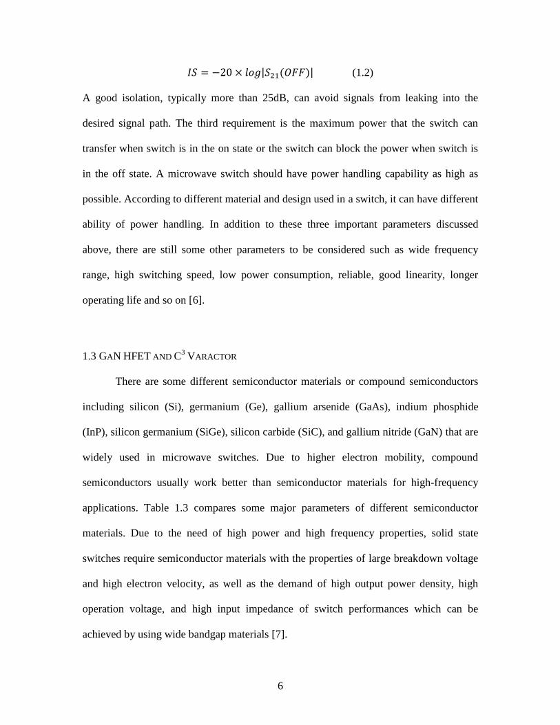
1.3 GAN HFET AND C3 VARACTOR
There are some different semiconductor materials or compound semiconductors
including silicon (Si), germanium (Ge), gallium arsenide (GaAs), indium phosphide
(InP), silicon germanium (SiGe), silicon carbide (SiC), and gallium nitride (GaN) that are
widely used in microwave switches. Due to higher electron mobility, compound
semiconductors usually work better than semiconductor materials for high-frequency
applications. Table 1.3 compares some major parameters of different semiconductor
materials. Due to the need of high power and high frequency properties, solid state
switches require semiconductor materials with the properties of large breakdown voltage
and high electron velocity, as well as the demand of high output power density, high
operation voltage, and high input impedance of switch performances which can be
achieved by using wide bandgap materials [7].

7
Table 1.3:the comparison of major electronic properties of GaN to other semiconductors [7]
Si GaAs 4H-SiC GaN Diamond
1.1 1.42 3.26 3.39 5.45
11.8 13.1 10 9.0 5.5
1350 8500 700
1200(Bulk)
2000(2DEG) 1900
0.3 0.4 3.0 3.3 5.6
Gallium Nitride (GaN), having material properties such as high mobility, high
saturation velocity, high sheet carrier concentration and high breakdown field that can
provide high power for switches, also high heat capacity and thermal conductivity that
can provide good heat handling capability, and chemical inertness providing good
reliability, becomes a novel semiconductor material which can provide superior
performance for high-power and high-temperature microwave applications [8][9]. Thus
GaN has been used in making high power microwave switches, such as AlGaN/GaN
heterostructure field-effect transistor (HFET), AlGaN/AlGaN metal-oxide-semiconductor
heterostructure field-effect transistor (MOSHFETs), etc., which has demonstrated a good
performance in maximum power density, bandwidth, widely operation temperature range,
high switching power and high breakdown voltage[10]. Figure 1.2 shows the schematic
of a HFET structure, which will be used as base components for microwave switch.
HFET is a three terminals device, which is controlled by applying bias on the gate
terminal to deplete the two dimensional electron gas (2DEG) channel. A more detailed
working principle will be described in chapter3.

8
Figure 1.2 The schematic of a HFET structure
Traditional HFET devices were made with Ohmic source and drain contacts,
which increase the difficulty of making devices. Forming Ohmic contacts on GaN
material usually requires annealing temperature over 850ºC [11] which will reduce the
quality of the AlGaN/GaN heterostructure and form additional electron trapping center
that can degrade the device high frequency performance and device reliability. Ohmic
contacts also increase the complicity of the device process due to the face of difficulty in
making good ohmic contact on high Al content AlGaN, which can resulting in the high
contact resistance and the need of precise alignment. Another issue is related to the gate.
In order to avoid the gate breakdown, the space of source-gate and gate-drain need to be
high. However, this also increases the channel length and will cause the higher insertion
loss which is due to the higher ON-resistance. For purpose of overcome these issues, a
new device has been demonstrated.
A novel GaN varactor, namely GaN based voltage controlled capacitor, consisting
the design of capacitively couple contacts (C3), has been proposed and successfully

9
demonstrated an improved performance for a high power microwave switch [12]. The
schematic of the GaN varactor is shown in the Figure 1.3. Instead of using the traditional
ohmic contact, two electrodes with the design of C3 forms the GaN varactor between the
electrodes and the 2DEG channel. This type of design has many advantages such as the
device can be fabricated by using alignment-free technology which decrease the
complicity of device process and no need of annealing process preventing many devices
issues and performance degradation. GaN varactors also show higher microwave power
handling capability, and lower contact resistance as compare to Ohmic contact devices.
Furthermore, GaN varactors can be controlled its ON/OFF states by either applying
positive or negative voltage, instead of only negative voltage for traditional normally ON
HFET devices [10][12][13][14]. The above mentioned merits suggest that GaN varactors
are promising based device for the next generation microwave switch and related
communication systems.
Figure 1.3 The schematic of a C3 structure

10
1.4 ELECTROMAGNETIC SOFTWARE
Because of the increasing of the design for high frequency and high speed
complex electronic systems, engineers use electromagnetic (EM) simulation software to
pre-determine whether the system meet the design requirements. Microwave Electronic
Design Automation (EDA) simulation software is related with the EM field of different
numerical algorithms. Before we learn about microwave EDA software, we need to
know all the numerical algorithms are based on the Maxwell’s equations. Understanding
the Maxwell's equations is the first step to learn the numerical algorithms in EM field.
There are some numerical algorithms used in the frequency domain, such as finite
element method (FEM), method of moment (MoM), finite difference method (FDM),
boundary element method (BEM), and transmission-line-matrix method (TLM). Some
numerical algorithms used in the time domain, such as finite-difference time-domain
(FDTD), and finite integration technology (FIT). Different EDA simulation software
which can be classified into different groups according to the numerical analysis they are
used [15][16]. Table 1.4 listed the most common EDA simulation software in the market.
There is no an absolute advantage that which numerical algorithm has accuracy and
efficiency. Different algorithms have different strengths, and suitable for different
application.

11
Table 1.4: Common EDA simulation software in the market [15][16]
Numerical
algorithms software
MoM
Advanced Design System (ADS), Ansoft Designer,
Sonnet, Microwave Office, Zeland IE3D,
Ansoft Esemble, Super NEC and FEKO
FEM Ansoft HFSS, and the version after ADS 2008
FDTD EMPIRE and XFDTD
FITD CST Microwave Studio
In this thesis, I am using Ansoft HFSS to do EM modeling for microwave
switches. HFSS is one of the EM simulation software by using finite element method.
FEM is a full 3D algorithm which can be used in arbitrary shape of structure. It has
several advantages over MoM and can be applied to many applications such as the Bond-
wire or Solder-balls in the package structure, Z-axis direction arbitrary structure,
transition designs, and interconnect analysis. In addition, FEM can be calculated the
question of finite size substrates, such as the structure of the cavity [17]. However, the
simulation time of FEM is usually slower than MoM especially for multilayer planar
applications. In the FEM, a large structure is divided into thousands of small area and use
volumetric meshing in each sub-region with a local function. The geometric model is
automatically divided into a large number of triangular pyramids, and the center point of
the field quantities inside each triangular pyramid will be saved. Then, the Maxwell’s
equations can be transformed into a matrix problem and extract S-parameters of arbitrary
shape that are solved by using mathematical operations. The way of FEM estimate the
convergence is by comparing before and after operations results. If the error range is less
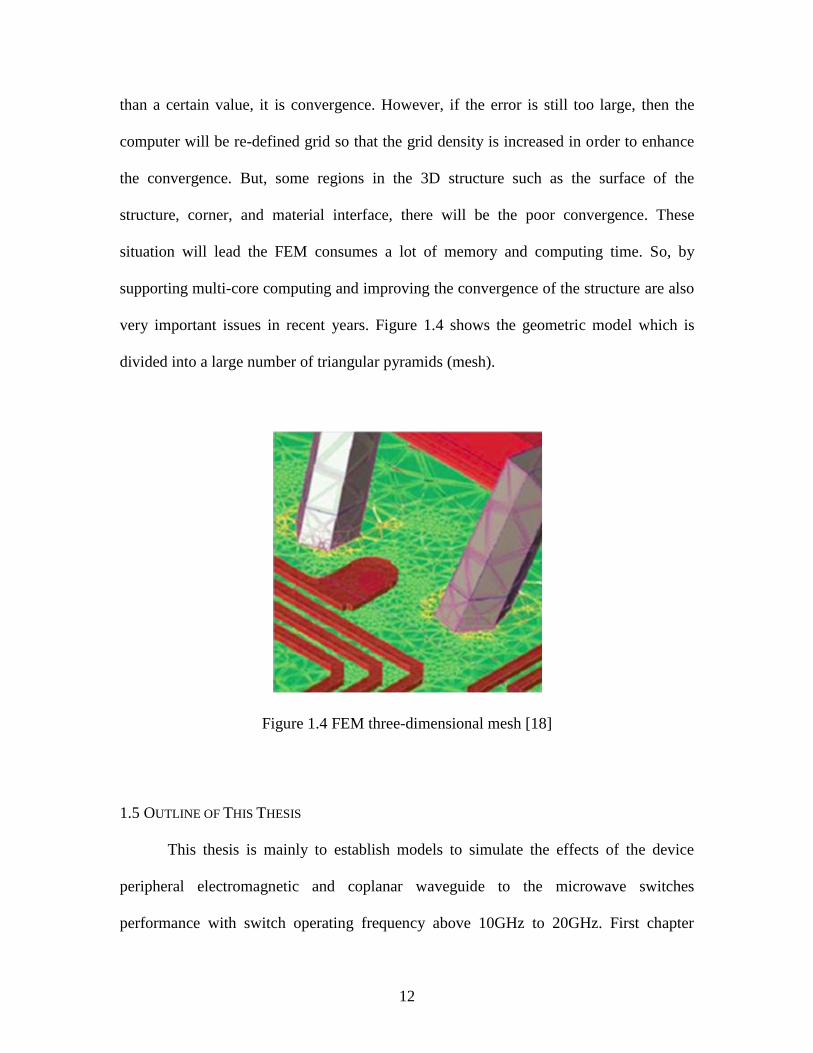
12
than a certain value, it is convergence. However, if the error is still too large, then the
computer will be re-defined grid so that the grid density is increased in order to enhance
the convergence. But, some regions in the 3D structure such as the surface of the
structure, corner, and material interface, there will be the poor convergence. These
situation will lead the FEM consumes a lot of memory and computing time. So, by
supporting multi-core computing and improving the convergence of the structure are also
very important issues in recent years. Figure 1.4 shows the geometric model which is
divided into a large number of triangular pyramids (mesh).
Figure 1.4 FEM three-dimensional mesh [18]
1.5 OUTLINE OF THIS THESIS
This thesis is mainly to establish models to simulate the effects of the device
peripheral electromagnetic and coplanar waveguide to the microwave switches
performance with switch operating frequency above 10GHz to 20GHz. First chapter

13
introduce the background of microwave switches, including its applications, types,
market availability and base transistors used in this thesis. The comparison of the
frequently used Microwave Electronic Design Automation (EDA) simulation software is
also stressed in this chapter. In the second chapter, the problem in the MATLAB
simulation methods is identified. Chapter3 introduces HFSS EM simulation software to
simulate HFET based microwave switches. The newly proposed GaN capacitively
coupled contact (C3) varactor based microwave switches, simulated by establishing HFSS
models, are performed in the chapter 4. Chapter 5 summarizes this thesis and point out
future works.
14
CHAPTER 2 PROBLEM IDENTIFICATION
2.1 PROBLEM IDENTIFICATION
It is important to develop a reliable simulation model for devices before the final
layout and fabrications, which can save time, cost and prevent experiment errors. In the
past, researchers have designed microwave switches by using Advanced Design System
(ADS), PSPICE and other tools employing circuit diagrams and equivalent circuits,
including the input power, device width and length, frequency range, bias and other
parameters that will affect the power go through the switches. Another way is using
MATLAB simulation which is programming the related device formula to simulate low
frequency large signal model to verify the design before final layout [16][17]. Our group
has published several papers by using ADS and MATLAB to accurately simulate III-
nitride microwave switches [18][19][20][21]. However, for higher frequency
applications, typically more than 10 GHz, the effects of electromagnetic wave scattering
and absorption become more significant than at lower frequencies. The simulation result
inaccuracy increases while the operating frequency raise. Figure 2.1 shows the insertion
loss comparative results of from the measurement of a real HFET SPST device and its
MATLAB simulation data. The MATLAB simulation results are well matched with the
device measurement data below 2GHz, however, the inaccuracy increases while the
operating frequency increases. In our case, the insertion loss at 10GHz shows a difference
of 0.5 dB, comparable to the loss itself.

15
In order to get more accurate device properties for microwave switches, a more
accurate simulation tool which can precisely simulate higher frequency microwave
switch, especially the effects of electromagnetic field to the device, is demanded.
Figure 2.1 The comparison results of insertion loss
This thesis adopts HFSS (High Frequency Structure Simulator) 3D structure
simulation to analyze the microwave switch performance. HFSS is the first commercial
electromagnetic field simulation software using a 3D structure. It provides a simple and
intuitive design interface, accurate and adaptive field solution, and electrical performance
analysis capabilities. It can calculate the S-parameters of 3D passive structures of
arbitrary shape and full-wave electromagnetic field. There are many results can be
calculated by using HFSS. For example, basic numerical solution of electromagnetic
fields and the open border issue, the problem of near-and far-field radiation, port

16
characteristic impedance and propagation constant, S-parameters and the corresponding
port impedance normalized S-parameters, and resonant solution.
Although HFSS has many advantages, there are still some issues to be overcome.
Compared with simulating a circuit diagram in ADS, HFSS cost more time which relate
to the specification of computer and operator system. In general, it saves the time when
you simulate a model which has a symmetrical structure.

17
CHAPTER 3 HFSS SIMULATION OF HFET MICROWAVE SWITCHES
3.1 INTRODUCTION
In this chapter, GaN HFET based switches with operating frequency at 10GHz,
including through, series and single pole single throw (SPST), will be simulated by
HFSS. These simulated results will be used to compare with MATLAB simulated results.
MATLAB simulation principles are to find the on-resistance ( ) from its equivalent
circuit, followed by applying the on-resistance to the insertion loss or isolation formula,
which is briefly described here. Figure 3.1 shows an equivalent circuit of a series HFET
microwave switch. During ON state, the on-resistance ( ) is given by:
(3.1)
Where is the contact resistance, , and can be expressed by ungated ( )
and gated ( ) channel sheet resistance, i.e. and
, , where , and are the gate-source space, gate-
drain space and gate length, respectively, and W is the device width. When the device is
fully turned on, . For a typical AlGaN/GaN HFET, the channel
sheet resistance is around 300Ω/sq. From equation 3.1, can be easily calculated by
giving the contact resistance, sheet resistance, source-drain space and the device width.
To find the insertion loss of this HFET microwave switch, equation 3.2 is mostly used,
where and .
.

18
(3.2)
For finding the isolation, equation (3.3) is used, where and f is the switch
operating frequency [21].
(3.3)
As described in the problem identification chapter, the MATLAB simulation result shows
larger error while the device operating at higher frequency.
(a) a cross-session view (b) an equivalent circuit
Figure 3.1 A HFET microwave switch
Instead of simply applying formula to the equivalent circuit which only concerns
the internal circuit, HFSS is able to simulate 3D structure, including its peripheral
electromagnetic field and parasitic effects by dividing the 3D structure to many
blocks(meshes) as shown in Figure 3.2, and finding the relation and interactive effects
between all the meshes.
Sapphire/Sic
GaN
Source DrainAlGaN
Gate
2DEG

19
Figure 3.2 The mesh generation of a HFSS through model
3.2 THROUGH
HFSS is used to first simulate simplest circuit structure, which has no transistors
or HFET devices embedded, namely through structure. Figure 3.3 shows HFSS layout
diagram of the through structure, which only contains one input and one output, where
the two ends are connected by a transmission line and the two red rectangles are grounds.
This through structure is used to verify that this coplanar waveguide has very low signal
loss, which can make sure this transmission line will not affect the overall performance
after embed the HFET devices to form a switch.

20
Figure 3.3 HFSS Diagram of through structure
Figure 3.4 expresses a very low insertion loss at frequency ranging from zero to
20GHz (approach 0dB). This indicating the structure is an ideal transmission line, since
all the signals from the input pass through the transmission line to the output. It can be
used as a base structure for the development of switch devices.
Figure 3.4 Through structure shows around 0dB insertion loss

21
3.3 SERIES STRUCTURE (100UM)
Series structure has one HFET device connecting the input and output, with total
device width of 100um, as shown in Figure 3.5. The fingers area means a HFET device
and the yellow portions between fingers represent 2DGE. Figure 3.6 (a) shows the HFET
cross section view and its HFSS simulation model in ON state. The HFET gate was not
drawn in the HFSS model, this is due to the resistance between the gate and 2DEG is
very small, thus we can assume the two metals are connected to become one piece and
the effect from the gate can be ignored. Figure 3.6(b) express the 2DEG disappeared,
meaning the HFET is in OFF state. The gate was not shown in the HFSS model either,
this is due to the depletion length and the 2DEG length was unknown under this state,
and we are unable to draw a correct dimension for the gate, depletion region and 2DEG.
Instead of putting the gate in the model, we compared the real device isolation to many
HFSS models which have different finger gaps (1 to 5um), using the finger gap (1um)
that shows the best matched result with real device as standard for the series structure
simulation and later HFSS SPST model simulation. The parameters of this model in
HFSS are set as in Table 3.1.
Figure 3.5 HFSS Series structure diagram

22
(a) HFET in the ON state (b) HFET in the OFF state
Figure 3.6 HFSS model design for HFET ON/OFF state
Table 3.1 Material parameter for HFET switch in HFSS
Conductance Permittivity Thickness
2DEG 300Ω/sq 9 0.2um
Finger 1 0.2um
Substrate N/A 9 500um
Figure 3.7(a) shows that the insertion loss of the series structure characterized by
HFSS simulation, MATLAB simulation and real device measurement. All the results are
showing an insertion loss of about 2dB at 10GHz. The device isolation during OFF state
is around -20dB for all the measured data at 10GHz as exhibited in the Figure 3.7(b).
Both insertion loss and isolation characterized by HFSS model, MATLAB simulation and
real device are well matched, indicating the HFSS model, MATLAB simulation can be
used in simulation this type device structures.

23
(a) (b)
Figure 3.7 Insertion loss and Isolation of series structure
3.4 HFET SINGLE POLE SINGLE THROW(SPST) SWITCH
Single pole single throw (SPST) switch is one of the most common switches in
the market. In this section, SPST switches containing different dimension sets of HFET
will be used to verify the correctness of the HFSS simulation model. The data will be
used to compare with the real device measurement and MATLAB simulation. Before
switches were fabricated, different dimension optimization of a MATLAB simulation
was used to find out the best combination of series and shunt device dimensions. Here
SPST switch with series and shunt dimension sets of 1.05mm/ 0.75mm and
0.4mm/0.4mm which shown best insertion loss and isolation results from MATLAB
simulation were chosen.
3.4.1 HFET SPST (1.05MM/0.75MM) DC-10 GHZ SWITCH
Figure 3.8 exhibits a SPST switch, consisting series HFETs with overall device
width of 1.05mm and shunt HFETs with total device width of 0.75mm (found using

24
MATLAB optimization). The insertion loss versus operating frequency curve of this
SPST device is shown in Figure 3.9(a). It shows a clear trend that the insertion loss
increases while the operating frequency increases. Usually the insertion loss is related to
the overall impedance. In the ON state, the on-resistance from the series is almost
frequency independent. Thus the increase of loss is resulted from shunt components,
where the impedance of the off state capacitance is frequency dependent. Also, the HFSS
model showing a well matched result to the real device at 10GHz operating frequency as
compared to the MATLAB simulations. The isolation is shown in Figure 3.9(b), which
also shows a better match for the HFSS model than the MATLAB simulation. The
increase of the isolation is also due to the increase of the overall impedance, which can be
easily explained by applying high frequency value to equation 3.3.
Figure 3.8 HFSS-SPST 1.05mm/0.75mm structure diagram

25
(a) (b)
Figure 3.9 Insertion loss and Isolation of HFET-SPST 1.05mm/0.75mm switch
3.4.2 HFET SPST (0.4MM/0.4MM) DC- 20 GHZ SWITCH
Another HFSS SPST switch model with HFET device width of 0.4mm at both
series and shunt portions is shown in the Figure 3.10. In order to get a good switch
performance at 20GHz, instead of 10GHz, we have used MATLAB simulation to find the
best match of series-shunt configuration, and the series-shunt dimension set of
0.4mm/0.4mm was chosen. Both the insertion and isolation by the HFSS simulation are
close to the real device performance at 20GHz. However, the insertion loss shows
significant error in the MATLAB simulation. This difference is due to reflections and
loss in the coplanar waveguide, not accounted for in MATLAB.

26
Figure 3.10 HFSS-SPST 0.4mm/0.4mm structure diagram
(a) (b)
Figure 3.11 Insertion loss and Isolation of HFET-SPST 0.4mm/0.4mm switch
In this chapter, we have successfully showed that HFSS is able to accurately
simulate the performance of simple through structure and HFET based series structure,
and SPST microwave switches by establishing HFSS models with operating frequency
ranging from 0 to 20GHz.

27
CHAPTER 4 HFSS SIMULATION OF GAN VARACTOR SWITCHES
4.1 INTRODUCTION
The concept of capacitively coupled contact (C3) used in HFET has shown much
higher microwave power handling capability and lower contact resistance as compared to
regular devices with annealed Ohmic contacts [11][13]. Our group have further combined
the concepts of voltage-controlled capacitor (varactor) in our GaN based HFET
microwave switch, and published first GaN capacitively-coupled contact (C3) varactors
based microwave switch for MMICs [12][22], which gives higher flexibility to tune the
source/drain spacing, since the gate has been removed and decrease the overall
impedance. The symmetrical C3 varactor also has advantages such as can be controlled
either by applying positive bias or negative bias, and no need of post annealing process
and gate alignment. The major difference between the traditional ohmic contact based
transistors to the capacitively coupled contact based varactor switches is that the later
does not require DC current flow through the device. Thus instead of flowing the current
through the ohmic contacts, which physically connected to the device channel, the C3
varactor pass the microwave signal through the 2DEG channel by generating strong
capacitively coupling effect between the metal electrode and the 2DEG channel, as
shown in the Figure 4.1.

28
Figure 4.1 Comparison structure of ohmic and C3
contact
As mentioned before that one of the advantages for using the C3 varactor is this
device can be controlled by applying either positive or negative bias. Figure 4.2(a) shows
a layout of C3 varactor device which can be turned off by applying voltage to either of the
contacts with voltage exceeding the contacts pinch-off voltage, typically for Schottky
contacts is around 3~4V as the case here, and around 6- 9V for metal-insulator-
semiconductor (MIS) type contacts. To find the device performance such as insertion loss
and isolation, it is prerequisite to find the device impedance, which can be extracted from
the device equivalent circuit, as shown in the Figure 4.2(b). The impedance of C3
varactor is defined by a series connection of capacitors, attributed to the two electrodes
and channel, and resistors, attributed to the contact resistance and 2DEG resistance. Also,
the existence of the C3 metal contacts and the 2DEG channel, an RC transmission line is
formed between them. And thus the total varactor impedance at zero bias can be found
from equation 4.1 and 4.2:
(4.1)
;
(4.2)

29
Where is the C3 electrode impedance, is the propagation constant, is the
transmission line characteristic impedance, , d is the electrode spacing, f is
the operating frequency, is the channel sheet resistance, is the unit-area
capacitance between the electrode and the channel, and W are the electrode length and
width. While at a low frequency, , and C3 varactor impedance can be
approximated as a series resistor with one-third of the total channel resistance and a series
capacitor with the capacitance equals to a parallel capacitor of the same geometry, as
expressed in the equation 4.3 [12]:
(4.3)
The device insertion loss in ON state is related to channel resistance and the two
contact resistances, which can be reduced by improving growth and device fabrication
processes. Isolation in OFF state is related to the capacitance, which can be reduced by
reformation the device layout.
(a) the C3 varactor layout (b) impedance of C
3 varactor
Figure 4.2 The schematic of C3
varactor

30
In this chapter, we establish HFSS model to simulate the C3 varactor based
microwave switch at as high as 20GHz operating frequency. The MATLAB simulation
results and real device measurement results will be also to compare and verify the
correctness of the HFSS models.
4.2 C3 VARACTOR TEST STRUCTURE DESIGN & SIMULATION
Before starting the establishment of the HFSS model, it is important to understand
the principle behind switching the C3 varactor between ON and OFF state. In the
previous section, Figure 4.2 shows the layout of the C3 varactor, and points out that the
device is a normally ON device. To switch the device to OFF state, a voltage with a value
exceeding any of the electrodes pinch-off voltage is required.
C3 varactor is an active model, which is not able to simulation in HFSS. However,
in either the ON or OFF state, C3 varactor is composed of planar capacitors which are
formed by electrodes on the top and 2DEG layer on the bottom. In this behavior, two
HFSS models to simulating C3 varactor device ON and OFF state are built as shown in
Figure 4.3. During ON state, the 2DEG (yellow block) has the same length as the
dielectric (purple block), indicating the 2DEG is able to couple the single from the input
to the output. During the OFF state, namely an exceeding pinch-off positive voltage has
been applied to the right side finger, inducing more electrons to the right electrode and
further resulting in a depletion region (black block) below the dielectric. Thus the 2DEG
has shorter length resulting in the signal from the input cannot pass through the 2DEG
reach output, since the 2DEG is not long enough to reach the portion under the output
electrode.

31
Appling this ON and OFF simulation methods to microwave switch models which
has multiple fingers, two HFSS simulation models representing the multiple fingers
device ON and OFF states are exhibited in the Figure 4.3(b).
(a) Cross-section view of on/off satae
(b) HFSS Model
Figure 4.3 HFSS model design for C3
device ON/OFF state
After we built this model in HFSS, we use it to simulate for three simply C3
varactor series structures with three different device widths, which are 250um, 500um
and 1000um. The schematic of a C3 varactor series structure in HFSS is shown in Figure
4.4. For initial validation of this device concept, a multi-finger C3 varactor test structure
having the total width of 250, 500 and 1000 um with each electrode 2 um long and 50 um
wide was designed. The gap between the two electrodes was kept 2 um and the 2DEG
sheet resistance was 300 Ohm/Sq.

32
Figure 4.4 C3
series 250um structure diagram
The insertion loss results is showing in the Figure 4.5(a), where all the three
dimensions of the HFSS models are showing good matched to the experimental results
with an insertion loss of around -0.75dB~-0.25dB at 10GHz. Figure 4.5(b) also shows
well matched results of three different devices isolation for HFSS simulation and the real
device measurement. Both of the results have suggested that the establishment of the
HFSS model to simulation this type of microwave switch is able to precisely predict the
microwave switch performance.

33
(a) (b)
Figure 4.5 Insertion loss and Isolation of C3
Series structures
4.3 C3 SINGLE POLE SINGLE THROW(SPST) SWITCH (0.5MM/0.5MM)
In this section, C3 varactor based SPST microwave switch will be simulated. Like
previously mentioned in the HFET section, MATLAB simulation with different sets of
series and shunt device dimensions were used to find the best dimension combination
before the device to be fabricated. Here C3
SPST switch with series and shunt dimension
set of 0.5mm/ 0.5mm was chosen.
The microwave switch for this work was designed by our group using series-shunt
layout that is shown in Figure 4.6. The series and shunt C3 varactors have multi-finger
structure with 2 um electrode length, 2 um gap and single finger width W1=50 um. The
total width of the series and shunt varactors are both 0.5mm, i.e. WSER= WSHT = 10×W1 =
0.5 mm as optimized in MATLAB. For this design, we are able to get a very small off-
state capacitance with COFF = 0.15 pF/mm and to achieve minimal isolation of 25 dB at
18 GHz.

34
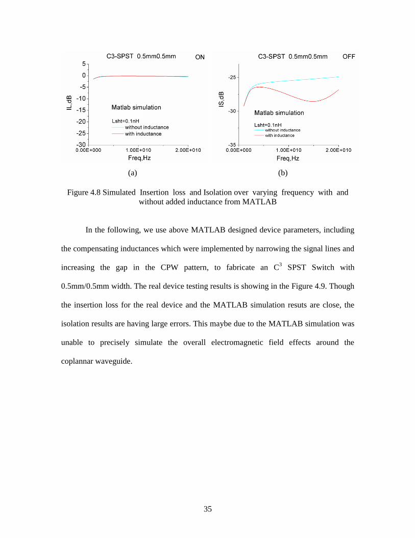
Figure 4.6 Series-shunt MMIC layout
Though from the above MATLAB design we were able to get an isolation of -
25dB at 18GHz, it is needed to further improve of isolation to increase the efficiency. In
order to decrease the simulated isolation, we have added inductances in series varactors
with an inductance value of 0.3nH and in shunt varactors with inductance value of 0.1nH
to compensate the capacitive component of the C3 impedance as shown in the Figure 4.7.
Figure 4.8 shows the insertion loss and isolation simulation results which clearly showing
that after adding the compensating inductance to the simulation device, a resonant
phenomenon occurs at 15GHz with an isolation as low as -28dB.
(a) equivalent circuit in ON state (b) equivalent circuit with L in OFF state
Figure 4.7 Equivalent circuit in ON and OFF states
35
(a) (b)
Figure 4.8 Simulated Insertion loss and Isolation over varying frequency with and
without added inductance from MATLAB
In the following, we use above MATLAB designed device parameters, including
the compensating inductances which were implemented by narrowing the signal lines and
increasing the gap in the CPW pattern, to fabricate an C3 SPST Switch with
0.5mm/0.5mm width. The real device testing results is showing in the Figure 4.9. Though
the insertion loss for the real device and the MATLAB simulation resuts are close, the
isolation results are having large errors. This maybe due to the MATLAB simulation was
unable to precisely simulate the overall electromagnetic field effects around the
coplannar waveguide.

36
(a) (b)
Figure 4.9 Insertion loss and Isolation of real C3
SPST switch
In order to provide a matched simulation results, we establish an HFSS model to
simulation the above fabricated device. HFSS model of the C3 SPST microwave switch is
shown in the Figure 4.10. The ON state insertion loss and OFF state isolation of
MATLAB, HFSS simulation and real device measurement are exhibited in the Figure
4.11(a) and Figure 4.11(b) respectively. Both of the results show that HFSS model can be
used to simulate the real device performance.
Figure 4.10 C3
SPST 0.5mm/0.5mm structure diagram

37
(a) (b)
Figure 4.11 Insertion loss and Isolation of C3
SPST 0.5mm/0.5mm switch
In order to get closer layout design to a real MMIC SPST switch, we also
established SPST model with smooth corner which is shown in Figure 4.12, where we
modified all the corners from a sharp shape to a curve shape as shown in the inset image.
In Figure 4.13, the simulation results of HFSS models with/ without smooth corner are
showing similar insertion loss and isolation, indicating the design of smooth corner will
not have major affects to the device performance. The establishment of HFSS model with
smooth corner will take more time to draw than that without smooth corner. Since the
smooth design did not show any differences from the sharp corner, we will keep using
sharp corner design to establish HFSS model.

38
Figure 4.12 C3
SPST 0.5mm/0.5mm structure diagram with smooth corner
(a) (b)
Figure 4.13 Comparison of insertion loss and isolation of C3 SPST 0.5mm/0.5mm switch
with/without smooth corner
After the successful demonstration of the real device performance by using HFSS
simulation, we would like to use HFSS to further design the switch layout to get a
resonance at different frequency. Since we have demonstrated from the MATLAB
simulation and shown that an additional inductance may induce a compensating
phenomenon, which can be implemented by narrowing the signal lines and increasing the
gap in the CPW pattern. Thus in the Figure 4.14, we are showing a modified C3 SPST

39
switch with an increased ground to signal line space to increase the compensating
inductance.
Figure 4.14 Modified C3
SPST 0.5mm/0.5mm structure diagram
The HFSS simulation results in the Figure 4.15 showing that the resonant
frequency was shifted from 23GHz to 19GHz, which indicates that we are able to
precisely simulate the resonant phenomenon, the space of the ground to signal line can
increase the inductance and the increase of the inductance can shift the resonant
frequency to a lower value. Thus we are able to use HFSS simulation to improve real
device design by modifying the imperfect capacitance compensation effect.

40
(a) (b)
Figure 4.15 Insertion loss and Isolation of modified C3 SPST 0.5mm/0.5mm switch
The above simulation results suggest that the establishment of HFSS model is
able to simulate simple structures such as through, series and SPST microwave switches.
HFSS simulation is also able to provide a higher accuracy than the commonly used
MATLAB simulation. Since HFSS simulation considers not only the transistors
themselves, but also the peripheral electromagnetic field. It is automatically dividing the
established HFSS model to many small blocks (meshes), and summarizing the effects
between each mesh.
4.4 C3 SINGLE POLE DOUBLE THROW(SPDT) SWITCH
In this section, C3 varactor SPDT switch will be discussed. Unlike SPST, which
has only one output, SPDT is a three ends switch, containing one input and two outputs,
which increases switch functionality. A more complicated device is expected to have
more coupling effects, which will increase the difficulty and inaccuracy of the simulation.

41
4.4.1 C3 SPDT SWITCH (0.25MM/0.2MM)
Figure 4.16 express an SPDT HFSS model, where signals go from top input to
either one of the side outputs. Here assume A end switch is ON and 2DEG appear at the
two circles region. This switch has C3 varactors with device width of 0.25mm at the
series portion and 0.2mm at the shunt portion. As mentioned before, the series and shunt
configureation plays a strong funtion to the switch performance. The increase of the shunt
width will improve the isolation, however, that will also increase the insertion loss due to
the increased off-capacitance caused from the larger width. Different sets of series- shunt
dimensions were used to find the best match for switch performance. There exists a large
gap between the signal and ground in the model, this is due to the need of placing the
input and two outputs contact pads.
Figure 4.16 C3
SPDT 0.25mm/0.2mm structure diagram
Insertion loss results are showing in the Figure 4.17(a), where HFSS result is
showing around -2dB, experimental result is around -1.2dB and MATLAB is showing -
0.5dB at 10GHz. Both HFSS and MATLAB shows errors as compare to the experimental
A ON B OFF
2DEG

42
data. However, MATLAB shows a smaller insertion loss than the real device. This can be
explained that due to MATLAB simulation did not consider the peripheral
electromagnetic field and coupling effects from the coplanar waveguide. When the
operating frequency increases, the difference becomes much smaller and the results
match at around 20GHz. The isolation data is exhibited in the Figure 4.17(b). HFSS
simulation also shows a better match to the experimental results while operating at the
higher frequency, where both of the data shows the isolation ranging from -23dB to -
25dB at operating frequency from around 3GHz to 20GHz. However for the MATLAB
simulation data the isolation are ranging from -27dB to -32dB, which shows around 20%
difference to the experimental results. Furthermore, the MATLAB simulation incorrectly
predicts the isolation trend, where the data shows a resonant frequency at around 15GHz.
But, there are no resonant phenomenon exists for the experimental curve.
(a) (b)
Figure 4.17 Insertion loss and Isolation of C3 SPDT 0.25mm/0.2mm switch
43
The establishment of HFSS model to simulate microwave switch at operating
frequency at more than 10GHz is once again verified to be able to predict the loss
performance of the switch in not only simple, but also complicated structure. The
simulation accuracy increases while the operating frequency increases. In the following
section, we will modified the existing C3
SPDT 0.25mm/0.2mm switch and try to design
a new C3 varactor SPDT switch by establishing previously verified HFSS models.
4.4.2 C3 SPDT MODIFIED SWITCH (0.25MM/0.2MM)
An modified (from Figure 4.15 SPDT switch) SPDT HFSS model is shown in the
Figure 4.18. We have found out from the previous section that the real device shown a
worse performance as compare to its MATLAB simulation, and we assume the different
is due to the real deivce has on purposely design a large gap for the insertion of contact
pads. In this design, we would like to test the affects of filling up the bottom gray portion
air gap with the ground metal, also we would like to form the contact pads outside the
coplanar waveguide, since our previous HFET design shows that the contact pads formed
outside the waveguide will not affect the switch performacne. We predict that this will
help to eliminate the OFF state inductance impedance and may result in a decrease of
isolation.

44
Figure 4.18 C3
Modified SPDT 0.25mm/0.2mm structure diagram
Figure 4.19 exhibits the comparative results between the modified and un-
modified switch. The insertion loss did not show much difference after we fill the
additional ground to the device. However, the isolation for the modified structure
showing a large improvement. Also a device resonant phenomenon appears at frequency
of around 22GHz with an isolation of -42dB. We believe that this resonance is coming
from increased capacitance, since the distance between the signal line and ground has
been narrowed, causing a compensating effect and a resonance at the 22GHz operating
frequency.

45
Figure 4.19 Insertion loss and Isolation of C3 SPDT modified switch
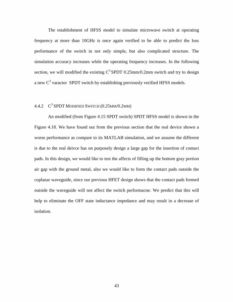
4.4.3 NEW DESIGN OF C3 SPDT SWITCH
In this section, we want to design a C3 SPDT Switch (0.25mm/0.2mm) with a new
coplanar waveguide layout. The structure diagram and design dimensions are showed in
fiqure 4.20. In order to save the simulated time, approach the future fabricated real device
performance and limit the errors which may caused by the complicated structure, we built
a symmetrical layout. The model is simulated while A port is ON. B port is OFF and thus
the 2DEG exist at the white circle region. The insertion loss results in the Figure 4.21
showing a value of -2.2dB at 10GHz, which is similar to the section 4.4.2 SPDT insertion
loss result. The isolation is also showing a resonant phenonmenon with a low isolation of
-41dB at the resonant frequency of 16GHz. We assume this resonant phenonmenon is due
the existance of additional compensating inductance coming from the interaction between
signal line A and siganl singnal line B. In the previous model, the two signal lines are too
far to induce obvious inductance. Another reason for the improved performance, may due
to the signal is parallelly transmit from the input to the output, instead of vertically
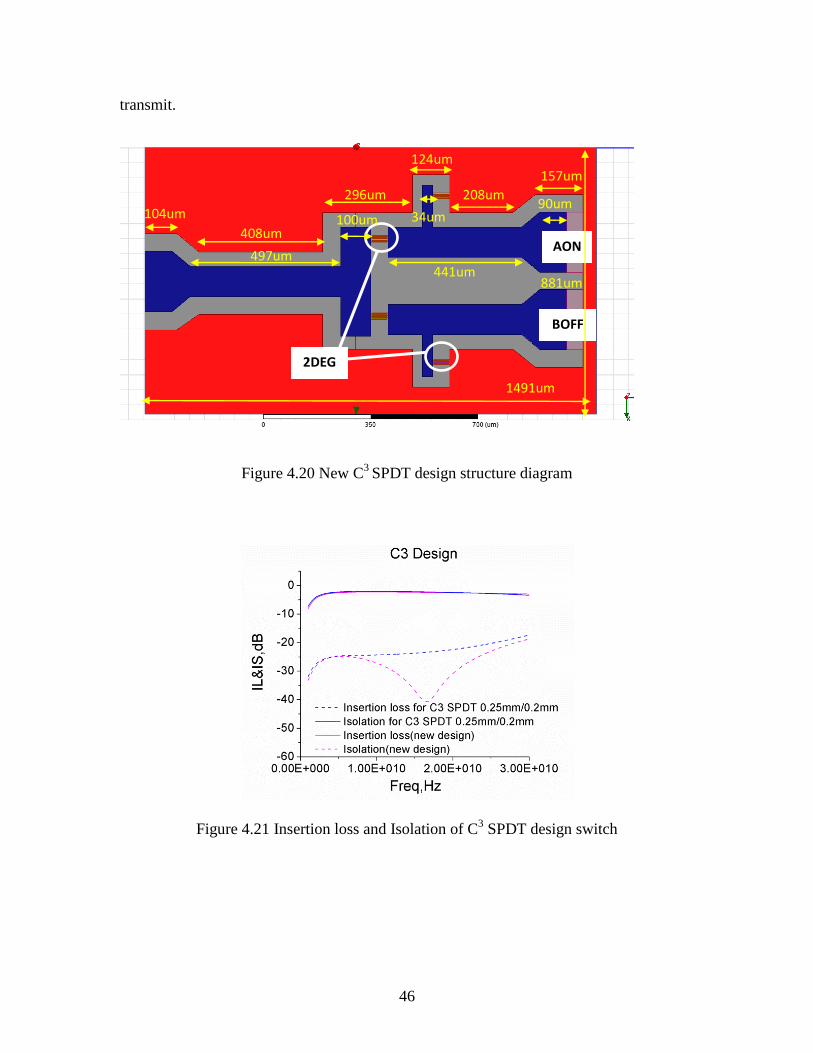
46
transmit.
Figure 4.20 New C3
SPDT design structure diagram
Figure 4.21 Insertion loss and Isolation of C3 SPDT design switch
1491um
34um
2DEG
AON
BOFF
881um
497um
100um
441um
90um 104um
408um
208um 296um
157um 124um

47
CHAPTER 5 CONCLUSION AND FUTURE WORK
5.1 CONCLUSION
This work presents the use of HFSS as a reliable electromagnetic simulation tool
to simulate the effects of the peripheral electromagnetic filed and coplanar waveguide
coupling effects to the GaN HFET and GaN C3 varactor based microwave switches.
Unlike other devices such as power amplifier, which has power loss more than 3dB, GaN
switch has outstanding performance with very low power loss less than 1dB. This low
loss value makes any scattering and loss in waveguides incorporating the device
becoming significant effect in the switch overall performance. Thus a simulation tool that
can precisely simulate low-loss microwave switches is needed. The Device performance
of structures like through, series, SPST and SPDT by using both HFET and GaN varactor
based components were accurately simulated by establishing HFSS models. The
structures were automatically divided by the software to many blocks or called meshes.
The interactions and effects between these meshes were summarized, containing other
parasitic effects from the peripheral metals. Although other simulation software, like
MATLAB and ADS, has quick response time and lower computer specification required,
they are not suitable to simulate high frequency microwave switch or devices, due to they
are unable to consider the overall switch structure effects and thus unable to accurately
simulate the real electromagnetic field effects.

48
In this research, we have shown that HFSS is able to simulate GaN HFET based
structures such as series and SPST switches with two different dimension sets,
1.05mm/0.75mm and 0.4mm/0.4mm, and GaN C3 varactor based structures. In addition
to show the ability of simulating the existing devices, HFSS simulation can be also used
to modify and design new microwave switches in either HFET or C3 varactor based
components. First, we presents a SPST model with smooth corner which can get closer
layout design to a real MMIC SPST switch and it indicates the design of smooth corner
will not have major affects to the device performance in HFSS. Second, we presents that
HFSS is used to simulate C3 varactor SPST switch and shows that by increasing the
ground to signal line space, which is believed to increase the compensating inductance,
and we are able to shift the resonant frequency. This can be used to tuning the RF switch
with a desired resonant frequency. Another example is showing a C3 varactor SPDT
switch with the filling of the ground metal is able to induce compensating inductance and
resulting in an occurrence of resonance with an isolation of -42dB at 22GHz. Thus we are
able to use HFSS to improve the device insertion loss and isolation by modifying the
model dimension or geometrical shape. Last, we also demonstrated the use of HFSS
simulation to design a new model with a descent insertion loss and isolation as low as of -
41dB at the resonant frequency of 16GHz. Table 5.1 shows the comparsion of three
different works with improved switch performance in this thesis.

49
Table 5.1 Comparison of three different works with improved switch performance
Modified C3 SPST
0.5mm/0.5mm
Modified C3 SPDT
0.25mm/0.2mm
New designed C3 SPDT
increasing space between
metal ground and signal line
filling the ground gap parallel input and output
design
Resonant frequency shift Resonant phenomenon
appear at 22GHz with
isolation of 42dB
New coplanar waveguide
design showing resonant
phenomenon with low
isolation of -41dB at
16GHz
5.2 FUTURE WORK
HFSS simulation will be used to modify existing structures to show a resonant
phenomenon for the device without resonance, used in tuning the resonant frequency to
the desired frequency and used to improve the isolation. HFSS will also be used to design
microwave switch with higher than 20GHz operating frequency. Furthermore, since the
compensating inductance is useful to coupling the capacitance and resulting in a resonant
phenomenon, different geometrical shape design for getting a higher inductive efficiency
will be studied. Last, instead of only used in HFET and C3 varactor, HFSS will be used to
simulate other structures, devices and systems.

50
REFERENCES
[1] G. Simin, A. Koudymov, Z.-J. Yang, V. AdivarahanS. Rai, J. Yang, and M. Asif
Khan, “High-power RF switching using III-nitride metal–oxide–semiconductor-
heterojunction capacitors,” IEEE Electron Device Lett., vol. 26, no. 2, pp. 56–58,
February 2005.
[2] Gary Breed, “A Review of RF/Microwave Switching Technologies,” High Frequency
Electronics, pp. 70-72, May 2010.
[3] G. M. Rebeiz, “RF MEMS switches: status of the technology,” IEEE Trans. The 12th
International Conference on Solid State Sensors, Actuators and Microsystems, Boston,
USA, June 2003.
[4] Pat Hindle, “The State of RF and Microwave Switches,” Microwave Journal, Vol. 53,
No. 11, pp 20-36, November 2010.
[5] Agilent Application Note, “Understanding RF/Microwave Solid State Switches and
Their Applications,” No. 5989-7618EN, May 2010.
[6] Sara Nazemzadeh, “A Guide To RF Switching Systems,” The RF & Microwave
Solutions Update, pp34 -44, June 2008.
[7] U. K. Mishra, L. Shen, T. E. Kazior, and Yi-Feng Wu, "GaN-Based RF power
devices and amplifiers" Proc. IEEE, vol.96, no.2, pp.287-305, Feb. 2008.
[8] TriQuint Semiconductor, Inc. “New GaN FETs, Amplifiers and Switches Offer
System Engineers a Way to Reduce RF Board Space and System Prime Power,”
Microwave Journal, 2012.
[9] M.D. Hodge, R. Vetury and J. Shealy, "A Robust AlGaN/GaN HEMT Technology for
RF Switching Applications" Compound Semiconductor IC Symposium, Waikoloa, pp. 1-
4, October 2011.
[10] Pengelly, R., S. Sheppard, T. Smith, B. Pribble, S. Wood, and C. Platis, Commercial
GaN devices for switching and low-noise applications, CS MANTECH Conference, Palm
Springs, CA, May 16--19, 2011.

51
[11] G. Simin , Z. Yang , A. Koudymov , V. Adivarahan , J. Yang and M. Khan "III-
Nitride transistors with capacitively-coupled contacts", Appl. Phys. Lett., vol. 89, no. 3,
pp.33510 2006.
[12] F. Jahan, Y-H. Yang, M. Gaevski, J. Deng, R. Gaska, M. Shur, and G. Simin, “2 –
20 GHz Switch using III-Nitride Capacitively-Coupled Contact Varactors,” IEEE El.
Dev. Lett, Vol.34 No.2, pp.208-210.
[13] G. Simin , Z.-J. Yang and M. Shur, "High-power III-Nitride integrated microwave
switch with capacitively-coupled contacts", Proc. IEEE/MTT-S Int. Microw. Symp.,
pp.457 -460 2007.
[14] G. Simin, B. Khan, J. Wang, A. Koudymov, M. Gaevski, R. Jain, J. Yang, X. Hu,
R. Gaska, and M. Shur "Multigate GaN RF Switches with Capacitively Coupled
Contacts", Electron Device Letters, IEEE, On page(s): 895 - 897 Volume: 30, Issue: 9,
September 2009.
[15] Guy A. E. Vandenbosch and Alexander Vasylchenko (2011). A Practical Guide to
3D Electromagnetic Software Tools, Microstrip Antennas, Prof. Nasimuddin Nasimuddin
(Ed.), ISBN: 978-953-307-247-0, InTech, DOI: 10.5772/14756.
[16] Van Hese, J., J. Sercu, D. Pissoort, and H. S. Lee, "State of the art in EM software
for microwave engineers," Agilent Technologies White Paper, Feb. 2009.
[17] Ansoft Corporation, HFSS v.13user guide
[18] Agilent Technologies, EMPro Workshop
[19] G. Simin, R. Gaska, and M. Shur. "Novel RF devices with multiple capacitively-
coupled electrodes." Microwave Symposium Digest, 2009. MTT'09. IEEE MTT-S
International. IEEE, 2009.
[20] G. Simin, B. Khan, A. Koudymov, M. Gaevski, R. Jain, J. Yang, X. Hu, R. Gaska,
and M. Shur, “Multigate GaN RF Switches With Capacitively Coupled Contacts,” IEEE
El. Dev. Lett, V. 30, N9 pp. 895-897, 2009.
[21] G. Simin, F. Jahan, J. Yang, M. Gaevski, X. Hu, J Deng, R. Gaska and M. Shur, “III
Nitride microwave control devices and ICs,” Smicond. Sci. Technol.28, 074008, 2013.
[22] F. Jahan, Y-H. Yang, M. Gaevski, J. Deng, R. Gaska, M. Shur, and G. Simin, “High
Performance RF Components Using Capacitively-Coupled Contacts Over III-N
Heterostructures,” Proceedings of 63rd IEEE Electronic Components and Technology
Conference, May 2013, pp.2002-2005.