electrolyte-based organic electronic...
TRANSCRIPT
Linköping Studies in Science and Technology
Licentiate Thesis No. 1330
Electrolyte-Based Organic Electronic Devices
Elias Said
LiU-TEK-LIC-2007:39
Dept. of Science and Technology
Linköping University, LiU Norrköping
SE-601 74 Norrköping
Norrköping 2007

LiU-TEK-LIC-2007:39
Printed by UniTryck, Linköping, Sweden 2007
ISBN: 978-91-85895-90-8
ISSN: 0280-7971
Abstract
The discovery of semi-conducting and conducting organic materials has opened new
possibilities for electronic devices and systems. Applications, previously unattainable for
conventional electronics, have become possible thanks to the development of conjugated
polymers. Conjugated polymers that are both ion- and electron conducting, allow for
electrochemical doping and de-doping via reversible processes as long as both forms of
conduction remain available. Doping causes rearrangement of the π-system along the polymer
backbone, and creates new states in the optical band gap, resulting in an increased electronic
conductivity and also control of the color (electrochromism). Doping can also occur by charge
injection at a metal – semiconducting polymer interface. Electrochemical electronic devices
and solid state devices based on these two types of doping are now beginning to enter the
market.
This thesis deals with organic based-devices whose working mechanism involves electrolytes.
After describing the properties of conjugated polymers, fundamentals on electrolytes (ionic
conductivity, types, electric double layer and the electric field distribution) are briefly
presented. Thereafter, a short review of the field of organic field effect transistors as well as a
description of transistors that are gated via an electrolyte will be reviewed.
Paper I present a novel technique to visualize the electric field within a two-dimensional
electrolyte by applying the electrolyte over an array of electronically isolated islands of
electrochromic polymer material on a plastic foil. By observing the color change within each
polymer island the direction and the magnitude of the electric field can be measured. This
technology has applications in electrolyte evaluation and is also applicable in bio-analytical
measurements, including electrophoresis. The focus of paper II lies on gating an organic field
effect transistor (OFET) by a polyanionic proton conductor. The large capacitance of the
electric double layer (EDL) that is formed at organic semiconductor/polyelectrolyte upon
applying a potential to the gate, results in low operation voltages and fast response. This type
of transistor that is gated via electric double layer capacitor is called EDLC-OFET. Because
an electrolyte is used as a gate insulator, the role of the ionic conductivity of the electrolyte is
considered in paper III. The effect on the electronic performance of the transistor is studied as
well by varying the humidity level.

A
Acknowledgements
The work presented in this licentiate thesis would not have been performed without many
help and support from some people.
Firstly, I would like to express my gratitude to my supervisor Prof. Magnus Berggren for
giving me the opportunity to work and study at one of the most outstanding research areas and
environments as well as for all his help and support. I would like also to thank my co-
supervisor Assoc. Prof. Xavier Crispin, who always had time for me when I needed help, for
his patience, support and encouragement. Thank you Xavier for all the help with this thesis.
Thanks go to my co-supervisor Docent Nathaniel D. Robinson for all guidance and support,
and for all time he has spent helping me and answering my questions.
Special thanks to the Organic Electronic research group that consists of Magnus, Xavier,
Sophie, PeO, Peter, Payman, Joakim, Fredrik, Lars, Oscar, Maria and the recently joined
members; Isak, Klas, Xiangjun, Georgios, Daniel, Yu and Hiam, for many valuable
discussions, great friendship and after-work leisure activities. I should not forget thanking the
former members of the Organic Electronic group Dr. David, Dr. Max, Docent Nate, Emilien
and Linda. Thank you Sophie for all the administrational help. I would also like to thank the
personal at ACREO for all help I got in the lab.
Thanks to a lot of people at ITN for various reason: Prof. Stan Miklavcic in guidance of my
first work at ITN, Dr. George Baravdish for giving me the opportunity and helping me
teaching, Mari Stadig-Degerman for all the fun we had in the preparation and teaching Kemi
A for Basåret, Frédéric Cortat and Martin Evaldsson for all the fun and discussions in various
subjects.
I want to thank my friends Allan Huynh, Mattias Andersson and Henry Behnam for their
friendship.
Finally, I would like to thank my dear father and mother; David and Sara, my brothers;
Maurice and Robert, and my sister with family; Lilian, Simon and little David, for their love,
joy and support.
Elias Said, Norrköping, September 2007

A

List of included papers
Paper I:
Visualizing the Electric Field in Electrolytes Using Electrochromism from a Conjugated
Polymer
Elias Said, Nathaniel D. Robinson, David Nilsson, Per-Olof Svensson, Magnus Berggren
Electrochemical and Solid-State Letters, 8 (2) H12-H16 (2005)
Contribution: All the experimental work except the theoretical result. Wrote the first draft and
was involved in the final editing of the paper.
Paper II:
Polymer field-effect transistor gated via a poly(styrenesulfonic acid) thin film
Elias Said, Xavier Crispin, Lars Herlogsson, Sami Elhag, Nathaniel D. Robinson and Magnus
Berggren
Applied Physics Letters, 89, 143507 (2006)
Contribution: All the experimental work. Wrote the first draft and was involved in the final
editing of the paper.
Paper III:
Role of the ionic currents in electrolyte-gated organic field effect transistors
Elias Said, Oscar Larsson, Magnus Berggren and Xavier Crispin
Manuscript
Contribution: All the experimental work. Wrote the first draft and was involved in the final
editing of the paper.

Contents
Contents
1 INTRODUCTION TO PLASTIC ELECTRONICS 1
2 POLYMERS: FROM INSULATORS TO CONDUCTORS 3
2.1 BACKGROUND 3 2.2 ELECTRICAL PROPERTIES (CONDUCTIVITY) OF CONJUGATED POLYMERS 5 2.3 TRANSPORT OF CHARGE CARRIES IN CONJUGATED POLYMERS 6 2.4 PROPERTIES OF CONJUGATED POLYMERS 8 2.4.1 ELECTROCHROMISM 8 2.4.2 ELECTROLUMINESCENCE AND PHOTOVOLTAIC EFFECT 10 2.5 EXAMPLES OF SPECIFIC CONJUGATED MATERIALS 10 2.5.1 POLY(3,4-ETHYLENEDIOXYTHIOPHENE) 10 2.5.2 POLY(3-HEXYLTHIOPHENE) 12 2.5.3 POLYANILINE 13
3 ELECTROLYTES 15
3.1 SOLID ELECTROLYTES 16 3.1.1 POLYMER ELECTROLYTES 16 3.1.2 POLYELECTROLYTES 17 3.2 ELECTRIC DOUBLE LAYER CAPACITORS 17 3.3 ELECTRIC FIELD IN ELECTROLYTES 20
4 ORGANIC FIELD EFFECT TRANSISTORS 21
4.1 WORKING PRINCIPLES 21 4.2 DEVICE STRUCTURES AND SEMICONDUCTOR MATERIALS 23 4.3 OFET CHARACTERISTICS 24 4.4 ELECTROLYTE-GATED OFETS 26 4.5 HUMIDITY EFFECT 29
5 SUMMARY OF THE INCLUDED PAPERS 31
5.1 PAPER I 31 5.2 PAPER II 31 5.3 PAPER III 32
6 REFERENCES 33
PAPER I 39
PAPER II 55
PAPER III 65

Introduction to Plastic Electronics
1 Introduction to Plastic Electronics
Since discovery of the world’s first transistor in 1947, thin film transistors made of inorganic
semiconductor materials, such as silicon, are today dominating the electronic industry.
Nowadays the processing methods for fabricating modern devices become increasingly more
complex resulting in higher production cost. Because the size of transistors becomes very
small, the device density, on for example processor chips, is increased giving rise to cost
reduction (per transistor). However, the transistor size is now approaching critical dimensions
that give rise to short channel effect in transistor channel (< 100 nm) or electron tunneling for
very narrow channel (< 30 Å). Beside the high cost that limits the range of applications in
daily life applications, their poor mechanical flexibility also limits their use on applications
requiring flexible substrates.
When organic semiconductors and conductors became available, new outlooks for electronic
systems have been opened. Optoelectronic devices that were previously thought to be
unsuitable in some applications, such as food industry, are now brought closer to nearly every
product. For instance they can be produced on plastic substrates and applied on packages.
Compared to silicon based components, organic based electronic devices as a promising
future despite their lower performance as a semiconductor because of several unique
properties of organic materials. First, many of them can be processed in solution and do not
require high purity levels. This makes possible to produce components using conventional
printing techniques, which allows large area, high volume and low-cost applications. In
comparison, building a silicon chip usually takes weeks of work and requires ultra clean
working environment. Organic devices can be faster produced under less carefully controlled
conditions. Second, organic devices can be made and integrated together with other
applications simultaneously. For example an organic sensor device that is woven in textile.
Third, they are flexible and light. Because the devices are made by thin films, they become
lightweight. It will be a weight reduction when an electronic news papers replace the
conventional news papers, because of less materials are used in production (up to 80% paper
reduction according to plastic logic, www.plasticlogic.com). Thanks to these features, the
organic electronic industry is expected to become as big as the silicon industry and will have a
large impact on our daily life.
1
Introduction to Plastic Electronics
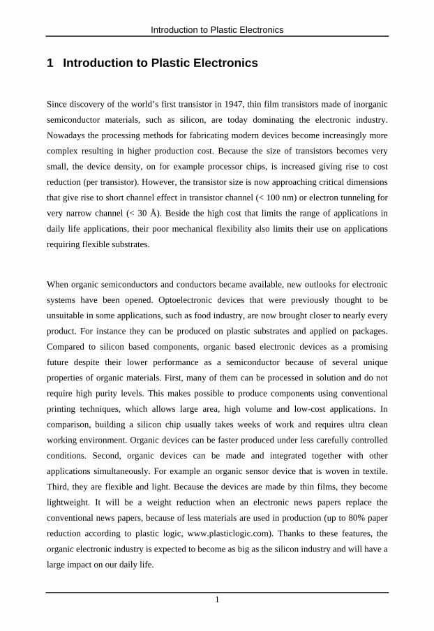
Figure 1. A mobile device rollable polymer display for reading personal information,
newspapers and books (By Polymervision, see www.polymervision.com).
One of the earliest applications of conductive polymer was to produce antistatic coatings,
lightweight batteries and materials for circuit boards. Today, few of organic (opto)electronic
devices start to move from R&D and labs into the market; such that in the next couple of
years low cost and even disposable plastic electronic devices will emerge. Already displays
that use organic light-emitting diodes (OLED) are found on the market. Another example of
polymer displays that entered the market is shown in figure 1. Unlike conventional displays,
polymer display can be rollable, which enables for instance mobile devices to incorporate a
display that is larger than the device itself. It should be noted that plastic electronics never
will match the switching speed and miniaturization of conventional electronics but they will
complete and go to places that conventional semiconducting industry cannot reach.
This thesis deals with organic based-devices whose working mechanism involves electrolytes.
After describing the properties of conjugated polymers in chapter 2, fundamentals on
electrolytes (ionic conductivity, types, electric double layer and the electric field distribution)
are briefly presented in chapter 3. Chapter 4 gives a short review of the field of organic field
effect transistors as well as a description of transistors that are gated via an electrolyte.
2
Polymers: From Insulators to Conductors
2 Polymers: From Insulators to Conductors
2.1 Background
Polymers that are assigned as conventional polymers, even called plastics, have been
considered under long time as insulators. At the beginning, polymers served in clothes, tools,
plastic bags, wire shielding and many others applications1. A huge interest in polymer science
started when important discoveries concerning modification and creation of semi-synthetic
polymeric materials as rubber were made from natural polymers. This gave later rise to the
development of a large number of fully-synthetic polymers, such as polystyrene and
poly(methyl methacrylate). Polymers are macromolecules that are formed by linking together
monomers in a chain through chemical reaction known as polymerization2. The formed
polymer chains can have linear, branched or a network structure.
The main element in many polymers is the carbon atom C. The valence electron configuration
for a C atom is 2s22p2 or 2s22px12py
1. With this configuration, the C atom can form two bonds
and not four with other atoms. Forming four bonds require that one 2s electron is excited to an
orbital with higher energy leading to the configuration 2s12px12py
1pz1. This process is called
promotion3. The unpaired electrons in separate orbitals of the promoted C atom can be paired
with other four electrons in orbitals that are provided by four other atoms. Notice that
excitation of the 2s electron to a higher orbital requires an investment of energy. But for C
atom case the energy is more than recovered when forming four bonds instead for two with
other atoms. This model was historically introduced like this and still is used when one
describes the C atom. However, it should be noted that this just is a model and doesn’t
represent the reality. The C atoms in polyethylene chain, which consists of a monomeric
repeat unit -(CH2 – CH2)n- are sp3 hybridized and each C atom binds to other four adjacent
atoms by sigma (σ) bond (figure 2.1a). The wavefunction of the σ-electrons are formed by the
large overlap between the sp3 hybrid atomic orbitals, which in turns form wide σ-bands, but
also large bandgap between the σ-band and the σ*-band. For polyethylene, the optical
bandgap is on the order of 8 eV4. The high bandgap makes conventional polymers electrical
insulators.
3
Polymers: From Insulators to Conductors
σ orbital π orbital
a)
b)
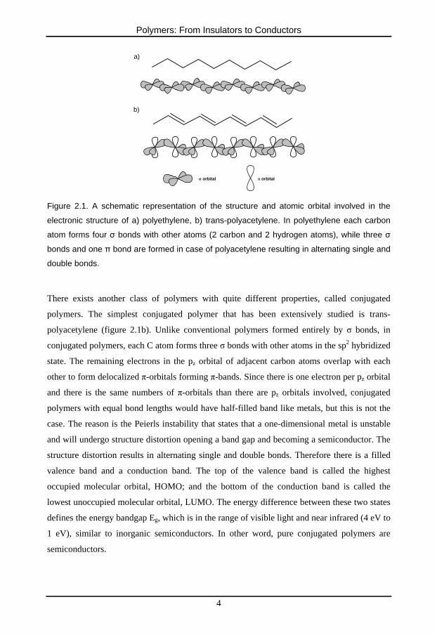
Figure 2.1. A schematic representation of the structure and atomic orbital involved in the
electronic structure of a) polyethylene, b) trans-polyacetylene. In polyethylene each carbon
atom forms four σ bonds with other atoms (2 carbon and 2 hydrogen atoms), while three σ
bonds and one π bond are formed in case of polyacetylene resulting in alternating single and
double bonds.
There exists another class of polymers with quite different properties, called conjugated
polymers. The simplest conjugated polymer that has been extensively studied is trans-
polyacetylene (figure 2.1b). Unlike conventional polymers formed entirely by σ bonds, in
conjugated polymers, each C atom forms three σ bonds with other atoms in the sp2 hybridized
state. The remaining electrons in the pz orbital of adjacent carbon atoms overlap with each
other to form delocalized π-orbitals forming π-bands. Since there is one electron per pz orbital
and there is the same numbers of π-orbitals than there are pz orbitals involved, conjugated
polymers with equal bond lengths would have half-filled band like metals, but this is not the
case. The reason is the Peierls instability that states that a one-dimensional metal is unstable
and will undergo structure distortion opening a band gap and becoming a semiconductor. The
structure distortion results in alternating single and double bonds. Therefore there is a filled
valence band and a conduction band. The top of the valence band is called the highest
occupied molecular orbital, HOMO; and the bottom of the conduction band is called the
lowest unoccupied molecular orbital, LUMO. The energy difference between these two states
defines the energy bandgap Eg, which is in the range of visible light and near infrared (4 eV to
1 eV), similar to inorganic semiconductors. In other word, pure conjugated polymers are
semiconductors.
4

Polymers: From Insulators to Conductors
2.2 Electrical properties (conductivity) of conjugated polymers
To increase the conductivity of the conjugated polymers, doping of these materials is
necessary. Doping can be obtained chemically via a redox molecule or electrochemically by
charge transfer with an electrode. The first high conducting polyacetylene was achieved via
chemical doping when a film of polymer was exposed to iodine vapor. Figure 2.2 illustrates
the range of conductivities for polyacetylene5 and other conjugated polymers compared with
other common materials. In electrochemical doping, the doping level is determined by the
applied voltage between the conducting polymer and the counter electrode. The doping charge
is supplied by the electrode to the polymer; while oppositely charged ions migrate from the
electrolyte to balance the electronic doping charge. This resembles an electrochemical cell.
Doping is reversible (if not kinetically blocked via one step in the mechanism). The
electrochemical doping of the π-polymer is illustrated by the following formulas:
(π-polymer)n + [M+X-]solution [(π-polymer)+yX-y]n + M electrode (p-type doping)
(π-polymer)n + [M]electrode [(M+)y(π-polymer)-y]n + [M+X-]solution (n-type doping)
Figure 2.2. Electrical conductivities of conjugated polymers compared with other common
materials.
As mentioned previously, electrochemically doping and undoping must involve counterion to
stabilize the doped state. Doping can also occur without involving any ions by charge
injection at a metal – semiconducting polymer interface. At the interface the polymer can be
5
Polymers: From Insulators to Conductors
oxidized upon hole injection into HOMO or reduced when electrons are injected into empty
bands. The induced charge carriers will lead to increase the electrical conductivity at the
polymer interface. However, this induced conductivity (or the doping) is maintained as long
as the carriers are injected (e.g. by applying the bias voltage). Upon removal the carrier
injection, the doped polymer at the interface returns to its original state. While in case of
electrochemical doping, the doping level is permanent until carriers are intentionally removed
by undoping.
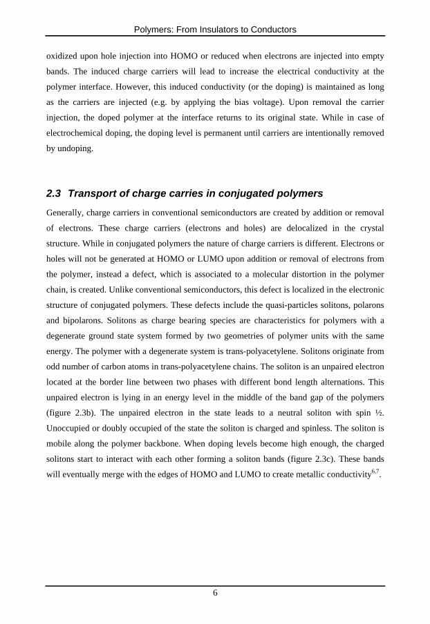
2.3 Transport of charge carries in conjugated polymers
Generally, charge carriers in conventional semiconductors are created by addition or removal
of electrons. These charge carriers (electrons and holes) are delocalized in the crystal
structure. While in conjugated polymers the nature of charge carriers is different. Electrons or
holes will not be generated at HOMO or LUMO upon addition or removal of electrons from
the polymer, instead a defect, which is associated to a molecular distortion in the polymer
chain, is created. Unlike conventional semiconductors, this defect is localized in the electronic
structure of conjugated polymers. These defects include the quasi-particles solitons, polarons
and bipolarons. Solitons as charge bearing species are characteristics for polymers with a
degenerate ground state system formed by two geometries of polymer units with the same
energy. The polymer with a degenerate system is trans-polyacetylene. Solitons originate from
odd number of carbon atoms in trans-polyacetylene chains. The soliton is an unpaired electron
located at the border line between two phases with different bond length alternations. This
unpaired electron is lying in an energy level in the middle of the band gap of the polymers
(figure 2.3b). The unpaired electron in the state leads to a neutral soliton with spin ½.
Unoccupied or doubly occupied of the state the soliton is charged and spinless. The soliton is
mobile along the polymer backbone. When doping levels become high enough, the charged
solitons start to interact with each other forming a soliton bands (figure 2.3c). These bands
will eventually merge with the edges of HOMO and LUMO to create metallic conductivity6,7.
6

Polymers: From Insulators to Conductors
Figure 2.3. a) The energy diagram of a neutral polymer chain. The difference between high
occupied molecular orbital (HOMO) and low unoccupied molecular orbital (LUMO) defines
the bandgap Eg. b) The oxidation and reduction of the neutral soliton (left) results in positive
(center) and negative (right) soliton. c) High redox-doping forms soliton band.
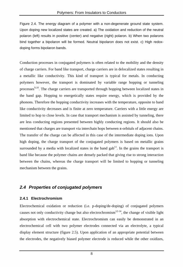
Most of conjugated polymer systems are non-degenerate ground state systems. In these
polymers the interchange of the single and double bonds produces higher energy geometric
configuration. Addition/removal of an electron on a neutral segment causes distortion and
formation of a localized defect that moves together with the charge. This combination of an
additional charge coupled to local lattice distortion is called a polaron8. Depending on the sign
of the charge remove, one speaks about positive polarons or negative polarons. The polaron
has a localized electronic state in the bandgap. Upon further addition of charges to the
polymer chain, two charges might couple together, despite electrostatic repulsion, thanks to
lattice distortion to create bipolarons. At high enough doping level a bipolaron band is formed
and eventually merges with the HOMO and LUMO bands respectively to produce partially
filled bands and metallic like conductivity. Unlike polarons, bipolarons are always charged
and have zero spin.
7
Polymers: From Insulators to Conductors
Figure 2.4. The energy diagram of a polymer with a non-degenerate ground state system.
Upon doping new localized states are created. a) The oxidation and reduction of the neutral
polaron (left) results in positive (center) and negative (right) polaron. b) When two polarons
bind together a bipolaron will be formed. Neutral bipolaron does not exist. c) High redox-
doping forms bipolaron bands.
Conduction processes in conjugated polymers is often related to the mobility and the density
of charge carriers. For band like transport, charge carriers are in delocalized states resulting in
a metallic like conductivity. This kind of transport is typical for metals. In conducting
polymers however, the transport is dominated by variable range hopping or tunneling
processes9,10. The charge carriers are transported through hopping between localized states in
the band gap. Hopping to energetically states require energy, which is provided by the
phonons. Therefore the hopping conductivity increases with the temperature, opposite to band
like conductivity decreases and is finite at zero temperature. Carriers with a little energy are
limited to hop to close levels. In case that transport mechanism is assisted by tunneling, there
are less conducting regions presented between highly conducting regions. It should also be
mentioned that charges are transport via interchain hops between π-orbitals of adjacent chains.
The transfer of the charge can be affected in this case of the intermediate doping ions. Upon
high doping, the charge transport of the conjugated polymers is based on metallic grains
surrounded by a media with localized states in the band gab11. In the grains the transport is
band like because the polymer chains are densely packed that giving rise to strong interaction
between the chains, whereas the charge transport will be limited to hopping or tunneling
mechanism between the grains.
2.4 Properties of conjugated polymers
2.4.1 Electrochromism
Electrochemical oxidation or reduction (i.e. p-doping/de-doping) of conjugated polymers
causes not only conductivity change but also electrochromism12-14, the change of visible light
absorption with electrochemical state. Electrochromism can easily be demonstrated in an
electrochemical cell with two polymer electrodes connected via an electrolyte, a typical
display element structure (figure 2.5). Upon application of an appropriate potential between
the electrodes, the negatively biased polymer electrode is reduced while the other oxidizes,
8

Polymers: From Insulators to Conductors
causing a color change in one or both of the electrodes. This doping/de-doping redox switch is
fully reversible and can be repeated many times15.
Figure 2.5. Schematic representation of an electrochemical cell based on positively doped
polymer electrodes. When a voltage is applied the positively biased polymer electrode is
oxidized while the other reduces. At the oxidized polymer electrode, the concentration of
positive (bi)polarons is increased, therefore anions A- (or cations C-) migrate into (out) the
polymer film in order to maintain the electroneutrality. On the contrary, the reduced electrode
undergoes a decrease of positive polaron and the migration of oppositely charged ions
occurs from the electrolyte. This type of cell is typically used as a display element.
Doping of the conjugated polymers causes rearrangement of the π-system along the polymer
backbone, and creates new states in the optical bandgap (polaron and bipolaron are formed
inside the bandgap), resulting in an increased electronic conductivity and also control of the
color change. This feature makes conjugated polymers useful in many applications as
displays16, smart windows17 and determining the direction and the magnitude of the electric
field in electrolytes18. The color change between doped and undoped forms of the polymer
depends on the magnitude of the bandgap of the undoped polymer. Thin films of polymers
with bandgaps greater than 3 eV are colorless and transparent in undoped form, but colored in
the doped state. While for bandgaps in order to or less than 1.5 eV, polymer films are colored
in undoped state and transparent in doped state, since the polaronic states create optical
absorption in the infra-red region. Polymers with intermediate bandgaps, as polypyrrole, will
switch between distinct colors. In case of polypyrrole, the color change is from yellow-green
(insulating) to blue-violet (conductive) upon reversible oxidation8.
9
Polymers: From Insulators to Conductors
2.4.2 Electroluminescence and photovoltaic effect
Electrochromism described in previous section occurs when the polymer film is
chemically/electrochemically doped in present of counter ions. In a typical polymer light
emitting diode, the conjugated polymer is not doped and sandwiched between two metal
electrodes. The hole injection at anode together with electron injection at the cathode result in
generation of positive and negative quasi-particles (polarons) in the polymer film. Each
particle is transported, thanks to the applied electric field present across the polymer film until
they meet and form an excited but neutral species called exciton. The relaxation of the exciton
to the electronic ground state takes place via light emission (i.e. radiative), called
electroluminescence; or via non-radiative decay. It is only a small amount of the excitons (~
25%) that contributes to light emission10. The wavelength of the emitted light can be tuned
within the visible region depending on which polymer is used.
Exciton can also be generated when a photon with an energy that is matched to the bandgap of
the polymer is absorbed. Recombination of the excitons will give rise to fluorescence. For
photovoltaic applications, the exciton (electron-hole pair) must be separated in a hole and an
electron and the recombination of the exciton is undesirable. Therefore the diffusion length of
the exciton should be long such that the exciton has a chance to meet an active centre (such as
a volume heterojunction) or an internal field, which gives rise to hole and electron
separation10. These charges will be then diffuse towards the electrodes. For organic solar
cells, efficiencies of 4-5% have been reached19.
2.5 Examples of specific conjugated materials
2.5.1 Poly(3,4-ethylenedioxythiophene)
Poly(3,4-ethylenedioxythiophene), abbreviated as PEDOT, is one of the most successful
conducting polymers, which was developed by the scientists at the Bayer AG research
laboratories in Germany20. PEDOT is synthesized by chemical or electrochemical
polymerization of EDOT monomers in an aqueous solution comprising the the electrolyte.
The positive doping charges carried by PEDOT is balanced by the counter anion poly(styrene
sulfonic) (PSS-). The resulting polymer blend PEDOT-PSS has been intensively investigated
and used in different research applications (figure 2.6). In the work presented in paper 1, thin
10

Polymers: From Insulators to Conductors
film of PEDOT:PSS, 200 nm thick (named OrgaconTM foil21) on plastic substrate has been
used.
Figure 2.6. The chemical structure of poly(3,4-ethylenedioxythiophene), PEDOT (lower part
of the figure) with poly(styrene sulfonic) acid, PSS-, as counterion (upper part). The positive
polaron responsible for the charge transport in PEDOT:PSS is also sketched.
Neutral PEDOT has a bandgap of 1.6 – 1.7 eV that makes it deep blue in color. The bandgap
can be controlled by using various oxidative agents giving rise to neutral polymers with colors
ranging over entire rainbow of colors20. Thanks to the low oxidation potential, films of neutral
PEDOT are not stable and oxidize rapidly in air. Therefore handling under an inert
atmosphere is required. In the doped and conducting (oxidized) state, PEDOT:PSS films with
conductivities between 1 and 10 S/cm are highly stable and have high transparency in the
visible region (strong near infrared absorption)22. The reduction formula of the doped PEDOT
is represented by the half reaction
−+−+−+ +→++ PSSMPEDOTeMPSSPEDOT :: 0
where +M denotes a positively charged ion and an electron. Reducing to the neutral state
results in a decrease in the number of charge carriers in PEDOT, giving rise to a decrease in
conductivity
−e
23 and a shift of the optical absorption spectrum from the near infrared region into
the visible region. The positive charge in doped PEDOT is delocalized over several monomer
11

Polymers: From Insulators to Conductors
units20. Thus, the representation PEDOT+ in the above equation is intended to represent a
group of consecutive monomer units.
The electrical conductivity of PEDOT can be enhanced through morphology change. For
example, conductivity of PEDOT:PSS has been increased three orders of magnitude when a
secondary dopant diethylene glycol (DEG) added to the PEDOT:PSS emulsion24. The origin
of the high conductivity is attributed to the phase separation of the excess PSS from the
PEDOT:PSS regions, which results in better pathways for conduction and an interconnected
three dimensional conducting network.
PEDOT:PSS was initially developed for antistatic applications in the photographic industry21,
but it took no long time to find the ability of this conducting polymer in other applications.
Thanks to its high stability and conductivity, easy processability and even the electrochromic
properties, PEDOT:PSS is a one of the promising candidate for developments in the area of
the cheap and flexible electronic systems. It can now be found as the electrode or conductor
material in electrochemical transistors25, organic field effect transistors26, organic light
emitting diodes27, electrochemical displays16, smart windows17, batteries and capacitors28,29.
2.5.2 Poly(3-hexylthiophene)
Polythiophene and its derivative, the poly(3-hexylthiophene) (P3HT) is one of the most
studied semiconducting polymer thanks to its good solubility and processability30. It is stable
both in doped and undoped state. The 3-hexyl substituent in a thiophene ring can be
incorporated into a polymer chain with two different regio-regularities31, shown in figure
2.7a: head to tail (HT) and head to head (HH). A regio-random P3HT consists of both HH and
HT 3-hexylthiophene in a random pattern, while a regio-regular P3HT (figure 2.7b) has only
one kind of 3-hexylthiophene, either HH or HT. Regio-regular P3HT has great potentials as
organic semiconductors in organic electronics because its strong tendency to self assemble
into crystallites with ordered structures upon casting into thin films, giving rise to carrier
mobilities in order of 0.1 cm2 V-1s-1 32. While the regio-random P3HT has a twisted chain
conformation with poor packing and low crystallinity, resulted in mobilities of only 10-4 cm2
V-1s-1 31 and higher optical band gap than its regio-regular structure has a lower bandgap. The
12
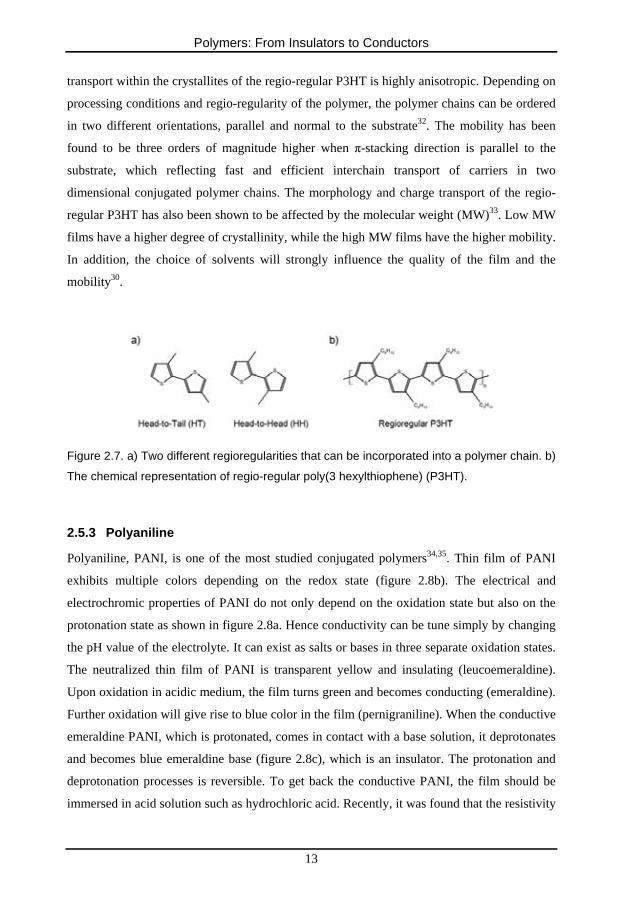
Polymers: From Insulators to Conductors
transport within the crystallites of the regio-regular P3HT is highly anisotropic. Depending on
processing conditions and regio-regularity of the polymer, the polymer chains can be ordered
in two different orientations, parallel and normal to the substrate32. The mobility has been
found to be three orders of magnitude higher when π-stacking direction is parallel to the
substrate, which reflecting fast and efficient interchain transport of carriers in two
dimensional conjugated polymer chains. The morphology and charge transport of the regio-
regular P3HT has also been shown to be affected by the molecular weight (MW)33. Low MW
films have a higher degree of crystallinity, while the high MW films have the higher mobility.
In addition, the choice of solvents will strongly influence the quality of the film and the
mobility30.
Figure 2.7. a) Two different regioregularities that can be incorporated into a polymer chain. b)
The chemical representation of regio-regular poly(3 hexylthiophene) (P3HT).
2.5.3 Polyaniline
Polyaniline, PANI, is one of the most studied conjugated polymers34,35. Thin film of PANI
exhibits multiple colors depending on the redox state (figure 2.8b). The electrical and
electrochromic properties of PANI do not only depend on the oxidation state but also on the
protonation state as shown in figure 2.8a. Hence conductivity can be tune simply by changing
the pH value of the electrolyte. It can exist as salts or bases in three separate oxidation states.
The neutralized thin film of PANI is transparent yellow and insulating (leucoemeraldine).
Upon oxidation in acidic medium, the film turns green and becomes conducting (emeraldine).
Further oxidation will give rise to blue color in the film (pernigraniline). When the conductive
emeraldine PANI, which is protonated, comes in contact with a base solution, it deprotonates
and becomes blue emeraldine base (figure 2.8c), which is an insulator. The protonation and
deprotonation processes is reversible. To get back the conductive PANI, the film should be
immersed in acid solution such as hydrochloric acid. Recently, it was found that the resistivity
13

Polymers: From Insulators to Conductors
of PANI film decreased when the temperature was lowered down to 5K indicating the
metallic behaviour of the film36. It is useful as a stable and low-cost conductor37,
electrochromic display window14, electrodes in organic transistors38, ion and pH sensors39 and
battery materials40.
Figure 2.8. a) The redox and protonation states of PANI. b) An image showing the multi
electrochromism properties of green protonated emeraldine film when it became oxidized
(pernigraniline) and reduced (leucoemeraldine). Notice that the PANI film was in contact with
a gelled electrolyte that in turn was connected to the outer electrodes. c) Deprotonation of
emeraldine film when immersing it in a solution with different pH. The contrast of the blue
color is strong at high pH levels.
14
Electrolytes
3 Electrolytes
The chemical compound that dissociate in ions in a solvent is called an electrolyte. Due to the
electrostatic interaction between solvent and the ions, the ions are surrounded by solvent
molecules. This process is commonly known as solvation. Electrolytes behave as electrically
conductive medium thanks to the solvated ions. Electrolytes can be found in liquid phase, but
also as molten electrolytes and solid electrolytes. Depending on the concentration of the salt,
the ionic conductivity might or might not vary drastically. Depending on the solute
dissociation that forms free ions, electrolytes are usually divided into two classes, strong and
weak electrolytes. In strong electrolyte (e.g., salts or strong acids), all or high amount of the
solute is dissociated and the ionic conductivity is quasi constant with the electrolyte
concentration. If the solute is partially dissociated in aqueous solution, the ionic conductivity
depends strongly on the solute concentration and this is called a weak electrolyte (e.g., weak
acids and bases). In addition, the choice of the solvent should be considered in
electrochemical applications. Each solvent has a defined potential window before it becomes
decomposed. For example water has narrow potential window (~3V) than acetonitrile
(~6V)41, which makes it not suitable for electrochemical measurements that require high
potentials.
The ionic conductivity, ĸ, of an electrolyte is given by
m)(inyResistivit1
Ω=κ , measured in S m-1
The ionic conductivity depends on the number of ions present and is usually expressed in
terms of the molar conductivity, defined via the relationship between the conductivity and the
concentration,
cκ
==ionConcentrattyConductivityconductiviMolar
The conductivity of the electrolytes can easily be measured using impedance spectroscopy
techniques42,43. For solid electrolytes, four probes techniques can also be used in measuring
the conductivity, which comes directly from
VLj Δ= /κ
15

Electrolytes
where j is the current density (current divided by the thickness t and width w of the
electrolyte), ΔV is the potential measured between two of the four fingers, and L is the
distance between the measured fingers. The ionic conductivity of solid electrolytes is usually
several orders of magnitude lower than the ionic conductivity of liquid electrolytes, because it
is limited by both low mobility and low concentration of ions. The ions in solid electrolytes
are introduced in a non-ionic matrix that conducts easily ions.
3.1 Solid electrolytes
Most solid electrolytes are polymer-based. The advantages of using solid electrolytes in
practical applications are many. The chemical and electrochemical stability and the flexibility
of the material makes it mechanically robust; thin films are easily processed on large areas.
Solid electrolytes are divided into two general categories: polymer electrolyte and
polyelectrolytes.
3.1.1 Polymer electrolytes
Polymer electrolytes are composed of a salt dispersed in a neutral polymer matrix (that is not
it-self an electrolyte)44. The salt is dissociated in ions screened by the polymer matrix. The ion
motion is coupled to local motion of polymer chain and transition between ion coordinating
sites44. The most studied polymer electrolytes are poly(ethylen oxide) (PEO) (figure 3.1a) that
consists of the repeating units of ether groups (-CH2CH2O-)n43,44 and its low molecular weight
polymer poly(ethylene glycol) (PEG)45,46. PEO is still one of the useful candidates in
designing new types of batteries47. PEO exhibits low ionic conductivity (10-9 - 10-8 S cm-1) at
room temperature because of its tendency to crystallize. Depending on the molecular weight,
the melting point of PEO varies from 60 oC for low weight to 66 oC. Thanks to the high
ability to dissolve high concentration of salts such as lithium and sodium salts, the crystalline
phase is suppressed enhancing the amorphous phase that results in higher ionic conductivity48.
PEO is soluble in water and a number of common organic solvents.
16

Electrolytes
Figure 3.1. a) The ether group repeating unit of poly(ethylene oxide) (PEO). b) Poly(styrene
sulfonate) (PSS-) with counter ion H+ (left) and Na+ (right).
3.1.2 Polyelectrolytes
Polyelectrolytes are polymers that bear ionized units49. The small mobile counter ions in
polyelectrolyte aqueous solutions dissociate making the immobile polymer chains charged.
The conductivity of aqueous polyelectrolyte solutions is in order of 0.1 µS cm-1 42. The
polyelectrolytes presented in Fig. 3.1.b are strong polyelectrolytes in solution. However, in
solid phase, because of the lack of screening solvent, the electrostatic potential attraction
between the immobile ions and the charged polymer chain is large and some mobile ions
remain bound to the polymer chains. This is known as a counter ion condensation
phenomena42,49 that divides the counter ions into bound and free counter ions. Bound counter
ions will stay in the vicinity of the charged polymer, while the free will dissociate from the
polymer chain and interacts through a screened Coulomb potential42. Poly(styrene sulfonate)
(PSS-) either with protons as counter ions or sodium (Na+) is displayed in figure 3.1b. Another
well-known proton conductor is NafionR. NafionR has been used as material for sensing
humidity in an electrochemical transistor50. When a nafionR film is exposed to water, it
becomes hydrolyzed allowing for effective proton transport across the film. Gelled PSS:Na
has been prepared as mixed together with other hygroscopic material to achieve higher ionic
conductivity in amorphous or semi-solid phase for using in electrochemical devices16,50,51.
The PSS:Na based electrolyte conductivity is in order of 10 µS cm-1 18.
3.2 Electric double layer capacitors
An interesting feature of electrolytes is its ability to form electric double layer capacitors
(EDLCs). Electrolytes are electron insulators but ionic conductors. Upon contact with two
oppositely charged ion-blocking electrodes sandwiching a common electrolyte (figure 3.2a),
the anions migrate towards the anode, while the cations migrate towards the cathode (figure
17

Electrolytes
3.2b). At the electrolyte/electrode interfaces, electrical double layers are then formed (figure
3.2c). The formed double layer can be seen as two-plate capacitor separated by a distance of
few angstroms, typically the thickness of the first solvation shell around the ions. Because of
this small distance, the capacitance of this model plate capacitor is large41. The resulting
EDLCs’ capacitance can reach high values, up to 500 µF cm-2 52. These capacitances are
almost independent on the thickness of the electrolytes, since the capacitors are formed in the
vicinity of the electrode surfaces. Thanks to charge separation that is formed within
microseconds EDLCs respond quickly to an applied electric field41. EDLCs can be
characterized using impedance spectroscopy. The effective capacitance for a capacitor with
poly(vinyl phosphonic acrylic acid) P(VPA-AA) electrolyte is of the order of 10 µF cm-2 at
100 Hz25.
Figure 3.2. The principle of the electric double layer capacitor (EDLC). a) A common
electrolyte is sandwiched between two ion blocking electrodes. At time t = 0 with no potential
difference between the electrodes, the ions are distributed uniformly in the electrolyte
medium. a) Upon applying a voltage at t = t1 anions (A-) start to move towards the positively
charge electrode, while the cations (C+) moves to the negatively charge electrode. c) After a
while at t2 > t1, the ions start to pack near the electrode interfaces giving rise to formation of
the electric double layer (EDL). The thickness of the double layer is in order of molecule size.
The structure of the electric double layer is currently described by Gouy-Chapman-Stern
(GCS) model41. The thicknesses of the double layer at the electrode and the electrolyte sides
are not the same, because of the charges at both sides are confined differently. However, it is
dominated by the electrolyte side. The interaction between solvated ions and the charged
18

Electrolytes
electrode is mostly electrostatic, while specific adsorption of ions may take place too. At the
electrolyte side double layer consists of a compact (Helmholtz) layer of ions next to the
electrode surface followed by a diffuse layer that extends into electrolyte bulk (figure 3.3).
Ions at different position in diffuse layer do not have the same energy due to the variation of
the electrostatic potential. Therefore the thickness of the diffuse layer will be varied when the
potential profile across the layer is modified. As the electrode potential becomes higher, the
diffuse layer becomes more compact. Also, the thickness is dependent on the ionic
concentration of the electrolyte. Higher ionic concentration gives rise to more compact diffuse
layer, i.e. the charges in electrolyte become more tightly compressed against the compact
layer. According to this model, the double layer equivalently is made of two capacitors in
series with capacitances representing both compact and diffuse layer. The potential profile
(solid curve) through the electrode side of the double layer according to GCS model in shown
as the inset in figure 3.3. The potential profile in the compact layer, shown in the figure 3.3, is
linear because of the assumption of constant capacitance of this layer (according to Helmholtz
model)41.
Figure 3.3. The arrangement of ions in the electric double layer (EDL) according to Gouy-
Shapman-Stern (GCS) model. The double layer is formed by a compact layer of ions next to
the electrode followed by a diffuse layer extending into bulk solution. The capacitance of the
EDL (Cd) is equivalently the total capacitance of both compact (CH) and diffuse layer (CD).
When CH >> CD the Cd is approximately equal to CD, while at very high CD the Cd is almost
the same as CH. The solid curve (as inset) shows the variation of the electrostatic potential
with distance from the electrode/electrolyte interface into the bulk. As in the GCS model, the
more concentrated the electrolyte is, the thinner is the diffuse layer.
19
Electrolytes
3.3 Electric field in electrolytes
The electric field in electrolytes has an important role on the performance of electrolyte-based
devices. For instance, the stability, selectivity and efficiency of polymer electrolyte fuel
cells53,54, batteries55 and electrochemical sensors50 depend on the electric field inside the
electrolyte. However, the field is difficult to be measured in real devices. Commonly, the field
is determined by measuring the potential along the electrolyte by electrical probes56 that are
coupled to external conducting lines. The difference in potential between the probes is then
taken to calculate the electric field. This measurement method usually requires considerable
hardware both for contacting the electrolyte and measuring the potential at each contact. The
resolution of the measurement is limited to the electrical connection i.e. the size of the probe
that can be manufactured.
20
Organic Field Effect Transistors
4 Organic Field Effect Transistors
Organic field-effect transistors (OFETs) have since the discovery in 198757 had a march of
progress. Nowadays OFETs have started to find applications that other conventional inorganic
transistors can not compete with. They serve as the main component in low cost and flexible
electronic circuits58. Their performance is now compared with that of amorphous silicon (a-
Si:H) transistors, which is widely used in large area applications such as active matrix liquid
crystal displays (LCDs). They offer a promising platform for many new opportunities e.g. for
flexible display back planes59,60 and integration of logic circuitry into low-cost electronic
products61. Prototypes that OFETs already have been demonstrated in such as radio frequency
identification tags (RFID)62-65 are now coming close to enter into the market.
4.1 Working principles
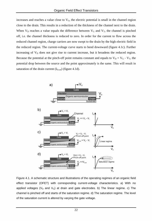
An OFET essentially consists of four different components: an electrical conducting material,
an insulating material, an organic semiconducting material and a carrier substrate (figure
4.1a). The organic semiconducting film that connects two electrodes, the source and drain
with a gap of length L and width W (channel dimension), is separated from a third electrode,
the gate by a thin film dielectric insulator. It can be seen as a two-plate capacitor placed
between two electrodes. The conductivity of one plate that lies between the electrodes is
altered by the voltage applied to the second plate of the capacitor. With no potential
difference between the source and drain (VD), applying a voltage to the gate (VG) charges are
injected from the grounded source electrode in the semiconductor and spread to charge the
capacitor at the insulator/semiconductor interface resulting in a doped conductive channel.
The density of the charges dependents on the gate voltage.
The operation mode of OFET is similar of conventional FET66 as illustrated in figures 4.1b-d.
The channel conductance is not only controlled by the potential on the gate, but also by VD.
Upon applying VG before VD the concentration of charge carriers in the channel is uniform. A
minimum voltage on the gate is often required to turn the channel on. This voltage is called
the threshold voltage (VT). When small VD is applied, the drain current (ID) follows Ohm’s
law, i.e. the channel conductance is constant. This is the linear regime (figure 4.1b). As VD
21
Organic Field Effect Transistors
increases and reaches a value close to VG, the electric potential is small in the channel region
close to the drain. This results in a reduction of the thickness of the channel next to the drain.
When VD reaches a value equals the difference between VG and VT, the channel is pinched
off, i.e. the channel thickness is reduced to zero. In order for the current to flow across the
reduced channel region, charge carriers are now swept to the drain by the high electric field in
the reduced region. The current-voltage curve starts to bend downward (figure 4.1c). Further
increasing of VD does not give rise to current increase, but it broadens the reduced region.
Because the potential at the pinch-off point remains constant and equals to VD = VG - VT, the
potential drop between the source and the point approximately is the same. This will result in
saturation of the drain current (ID,sat) (figure 4.1d).
Figure 4.1. A schematic structure and illustrations of the operating regimes of an organic field
effect transistor (OFET) with corresponding current-voltage characteristics. a) With no
applied voltages (VD and VG) at drain and gate electrodes. b) The linear regime. c) The
channel is pinched off and starts of the saturation regime. d) The saturation regime. The level
of the saturation current is altered by varying the gate voltage.
22
Organic Field Effect Transistors
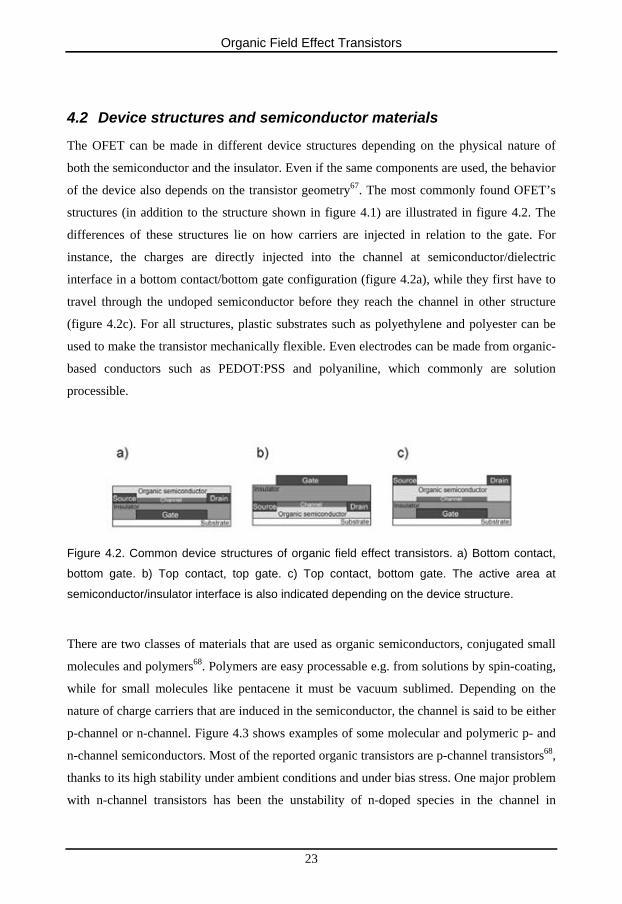
4.2 Device structures and semiconductor materials
The OFET can be made in different device structures depending on the physical nature of
both the semiconductor and the insulator. Even if the same components are used, the behavior
of the device also depends on the transistor geometry67. The most commonly found OFET’s
structures (in addition to the structure shown in figure 4.1) are illustrated in figure 4.2. The
differences of these structures lie on how carriers are injected in relation to the gate. For
instance, the charges are directly injected into the channel at semiconductor/dielectric
interface in a bottom contact/bottom gate configuration (figure 4.2a), while they first have to
travel through the undoped semiconductor before they reach the channel in other structure
(figure 4.2c). For all structures, plastic substrates such as polyethylene and polyester can be
used to make the transistor mechanically flexible. Even electrodes can be made from organic-
based conductors such as PEDOT:PSS and polyaniline, which commonly are solution
processible.
Figure 4.2. Common device structures of organic field effect transistors. a) Bottom contact,
bottom gate. b) Top contact, top gate. c) Top contact, bottom gate. The active area at
semiconductor/insulator interface is also indicated depending on the device structure.
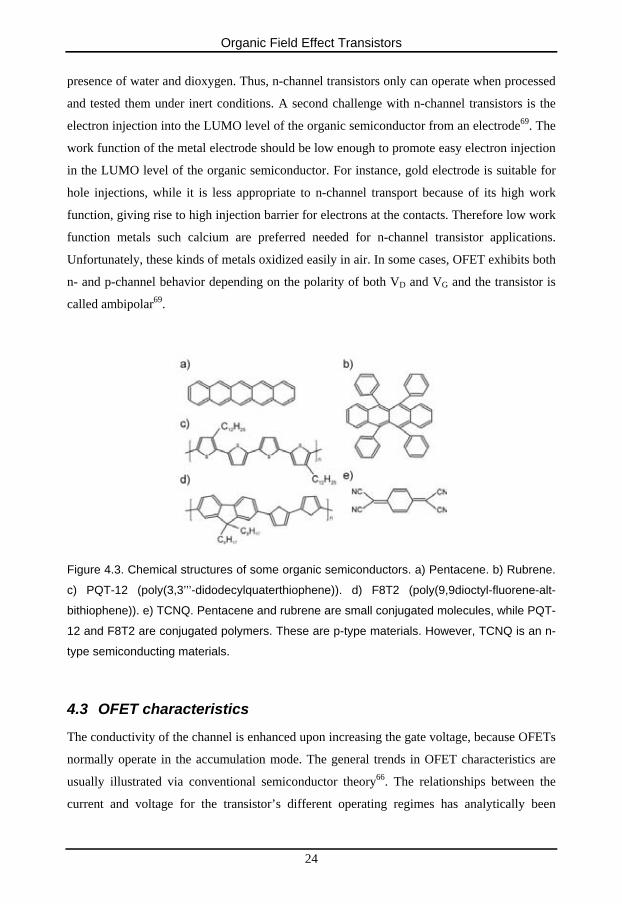
There are two classes of materials that are used as organic semiconductors, conjugated small
molecules and polymers68. Polymers are easy processable e.g. from solutions by spin-coating,
while for small molecules like pentacene it must be vacuum sublimed. Depending on the
nature of charge carriers that are induced in the semiconductor, the channel is said to be either
p-channel or n-channel. Figure 4.3 shows examples of some molecular and polymeric p- and
n-channel semiconductors. Most of the reported organic transistors are p-channel transistors68,
thanks to its high stability under ambient conditions and under bias stress. One major problem
with n-channel transistors has been the unstability of n-doped species in the channel in
23
Organic Field Effect Transistors
presence of water and dioxygen. Thus, n-channel transistors only can operate when processed
and tested them under inert conditions. A second challenge with n-channel transistors is the
electron injection into the LUMO level of the organic semiconductor from an electrode69. The
work function of the metal electrode should be low enough to promote easy electron injection
in the LUMO level of the organic semiconductor. For instance, gold electrode is suitable for
hole injections, while it is less appropriate to n-channel transport because of its high work
function, giving rise to high injection barrier for electrons at the contacts. Therefore low work
function metals such calcium are preferred needed for n-channel transistor applications.
Unfortunately, these kinds of metals oxidized easily in air. In some cases, OFET exhibits both
n- and p-channel behavior depending on the polarity of both VD and VG and the transistor is
called ambipolar69.
Figure 4.3. Chemical structures of some organic semiconductors. a) Pentacene. b) Rubrene.
c) PQT-12 (poly(3,3’’’-didodecylquaterthiophene)). d) F8T2 (poly(9,9dioctyl-fluorene-alt-
bithiophene)). e) TCNQ. Pentacene and rubrene are small conjugated molecules, while PQT-
12 and F8T2 are conjugated polymers. These are p-type materials. However, TCNQ is an n-
type semiconducting materials.
4.3 OFET characteristics
The conductivity of the channel is enhanced upon increasing the gate voltage, because OFETs
normally operate in the accumulation mode. The general trends in OFET characteristics are
usually illustrated via conventional semiconductor theory66. The relationships between the
current and voltage for the transistor’s different operating regimes has analytically been
24
Organic Field Effect Transistors
derived by assuming the gradual channel approximation: the electric field across the channel
(at the semiconductor/insulator interface ) is much larger than that along the channel (between
source and drain). These are given by:
( ) ( ) DDTGilinearlinearD VVVVCLWI )2/(/, −−= μ (eq. 4.1a)
( ) ( )2, 2/ TGisaturationsaturationD VVCLWI −= μ (eq. 4.1b)
where and is the drain current of the linear and saturation regime, W and L
the channel width and length, C
linearDI , saturationDI ,
i the capacitance per unit area of the insulator layer, µlinear and
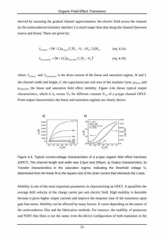
µsaturation the linear and saturation field effect mobility. Figure 4.4a shows typical output
characteristics, which is ID versus VD for different constant VG, of a p-type channel OFET.
From output characteristics the linear and saturation regimes are clearly shown.
Figure 4.4. Typical current-voltage characteristics of a p-type organic field effect transistor
(OFET). The channel length and width was 3.5µm and 200µm. a) Output characteristics. b)
Transfer characteristics in the saturation regime, indicating the threshold voltage VT
determined from the linear fit to the square root of the drain current that intersects the x-axis.
Mobility is one of the most important parameters in characterizing an OFET. It quantifies the
average drift velocity of the charge carrier per unit electric field. High mobility is desirable
because it gives higher output currents and improve the response time of the transistors upon
gate bias stress. Mobility can be affected by many factors. It varies depending on the nature of
the semiconductor film and the fabrication methods. For instance, the mobility of pentacene
and P3HT thin films is not the same; even the device configuration of both transistors is the
25
Organic Field Effect Transistors
same. Pentacene, which is vacuum deposited, has higher mobility (1.5 cm2 V-1s-1)70,71 than
regio-regular P3HT (0.1 cm2 V-1s-1)32, which directly is processed from a solution. The purity
of the material and the choice of solvent influence the mobility. Annealing the film after
deposition by spin-coating has been shown to give rise systematically to higher mobility due
to the complete removal of solvent in the semiconductor films. In some case, the enhancement
of mobility by annealing can be due to morphology change accompanied with a better
molecular packing72,73. It was also shown that the mobility is both drain and gated voltage
dependent74. From the equation above, the linear and saturation mobilities can be determined:
⎟⎟⎠
⎞⎜⎜⎝
⎛⎟⎟⎠
⎞⎜⎜⎝
⎛∂
∂=
DiG
linearDlinear VCW
LV
I ,μ (eq. 4.2a)
½½, 2)(
⎟⎟⎠
⎞⎜⎜⎝
⎛⎟⎟⎠
⎞⎜⎜⎝
⎛
∂∂
=iG
saturationDsaturation CW
LV
Iμ (eq. 4.2b)
Figure 4.4b shows a semilog plot of ID and square root of ID versus VG at constant VD in the
saturation regime, called transfer characteristics. The saturation mobility can easily be
calculated by extracting the gradient of the square root of ID. From transfer characteristics,
threshold voltage (VT) can be obtained by a linear fit to the square root of ID that intersects
with the VG-axis. Another important parameter that can be extracted from the transfer
characteristic is the On/Off current ratio, the ratio between ID in the on-state (at particular VG)
and ID in the off-state (at VG = 0V), ID,On/ID,Off. High On/Off current ratio is required for the
transistor to be integrated in circuits. The On/Off ratio for P3HT based transistor was obtained
as high as 106 75.
4.4 Electrolyte-gated OFETs
Most of organic semiconductor properties in OFET have been characterized using thermally
grown SiO2 as the insulator because of its ready availability. The use of these kinds of OFETs
in cheap electronics is not favorable, because of the requirement for very high operation
voltages. In order to make them applicable in electronics, the operation voltage should be
reduced without worsening the output current. The crucial parameter that governs the
operating voltage is the capacitance (per area) of the insulator Ci. From the relationship (eq
26

Organic Field Effect Transistors
4.1) between current throughput, gate voltage and capacitance it is clear that to obtain low
operating voltages, but keeping the output current high, Ci should be high. The capacitance
depends on both the dielectric constant (k) and the thickness of the insulator. Various kinds of
insulators with high capacitance have been investigated76: inorganic insulating materials with
high k such as aluminum oxide (Al2O3, k = ~10) and titanium oxide (TiO2, k = ~41), and
polymeric dielectric materials such as polyvinylalcohol (PVA, k = ~10) and polyvinylphenol
(PVP, k = ~4). In addition, self-assembled monolayer (SAM), which has a thickness of
molecular monolayer (~2 nm), has been used as a gate dielectric and the capacitance reached
the order of 1µF cm-1 77.
Beside their necessity of high capacitance, the insulating materials also should fulfill demands
specific to organic electronics i.e. low-cost, compatible with flexible substrates, processible
from solutions, insoluble in the solvent used for deposition of the organic semiconductor and
should be compatible with the gate electrode materials. Electrolytes have been found to be a
great materials to gate transistors (figure 4.5a)16,25,78-83. These types of dielectrics are usually
composed of a salt distributed in a solution or matrix, e.g., polymer gel. When a gate potential
is applied, the ions in the electrolyte redistribute and migrate into the semiconductor leading
to electrochemical doping (dedoping) in the bulk of the organic semiconductor. Thus, the
channel is opened (closed). These transistors are classified as electrochemical (EC) transistors
(Figure 4.5b). They can typically operate at low drive voltages (< 2 V) and be processed using
low-cost production techniques. But however, they respond slowly. One of the successful EC
transistors has been reported by Nilsson et al16. The presented transistor was based on lateral
architecture and the electrodes consisted only of a thin film of PEDOT:PSS on plastic
substrate, while a calcium chloride based gel was the electrolyte. The area that was covered
with electrolyte between the source and drain defined the channel. This resulted in all-organic
EC transistor. Here the conductivity of the channel was decreased upon applying a gate
voltage because of the reduction of the PEDOT:PSS channel, thus the On-state is defined at
zero applied gate voltage.
27
Organic Field Effect Transistors
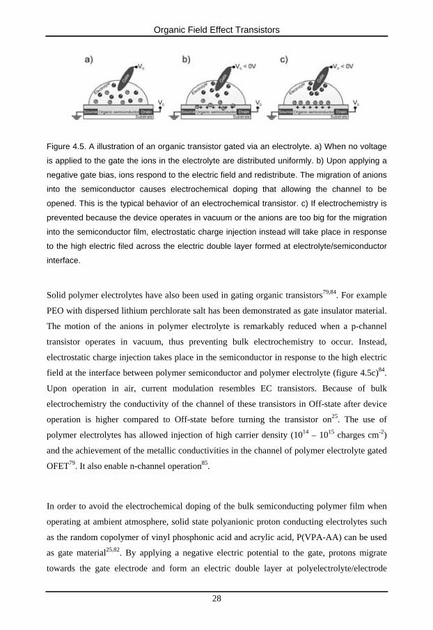
Figure 4.5. A illustration of an organic transistor gated via an electrolyte. a) When no voltage
is applied to the gate the ions in the electrolyte are distributed uniformly. b) Upon applying a
negative gate bias, ions respond to the electric field and redistribute. The migration of anions
into the semiconductor causes electrochemical doping that allowing the channel to be
opened. This is the typical behavior of an electrochemical transistor. c) If electrochemistry is
prevented because the device operates in vacuum or the anions are too big for the migration
into the semiconductor film, electrostatic charge injection instead will take place in response
to the high electric filed across the electric double layer formed at electrolyte/semiconductor
interface.
Solid polymer electrolytes have also been used in gating organic transistors79,84. For example
PEO with dispersed lithium perchlorate salt has been demonstrated as gate insulator material.
The motion of the anions in polymer electrolyte is remarkably reduced when a p-channel
transistor operates in vacuum, thus preventing bulk electrochemistry to occur. Instead,
electrostatic charge injection takes place in the semiconductor in response to the high electric
field at the interface between polymer semiconductor and polymer electrolyte (figure 4.5c)84.
Upon operation in air, current modulation resembles EC transistors. Because of bulk
electrochemistry the conductivity of the channel of these transistors in Off-state after device
operation is higher compared to Off-state before turning the transistor on25. The use of
polymer electrolytes has allowed injection of high carrier density (1014 – 1015 charges cm-2)
and the achievement of the metallic conductivities in the channel of polymer electrolyte gated
OFET79. It also enable n-channel operation85.
In order to avoid the electrochemical doping of the bulk semiconducting polymer film when
operating at ambient atmosphere, solid state polyanionic proton conducting electrolytes such
as the random copolymer of vinyl phosphonic acid and acrylic acid, P(VPA-AA) can be used
as gate material25,82. By applying a negative electric potential to the gate, protons migrate
towards the gate electrode and form an electric double layer at polyelectrolyte/electrode
28
Organic Field Effect Transistors
interface. The remaining immobile polyanion chains stay close to the positively doped organic
semiconductor, allowing the formation of p-channel. Because the polyanionic chains are
immobile, they cannot penetrate the semiconductor layer, thus preventing electrochemistry in
the bulk of the channel. Unlike EC transistors that require several of seconds to switch,
OFETs gated via electric double layer capacitor (EDLC-OFET) exhibit transients in kilohertz
region. The quick formation of double layers at polyelectrolyte/electrode and
polyelectrolyte/semiconductor interfaces result in low voltage operation (< 1V) and high
output current (in µA range for L/W=7/200). Employing polyelectrolytes as gate insulator, the
thickness of the insulator and the position of gate electrode become less important since the
EDLC spontaneously forms at insulator/semiconductor interface upon applying a gate bias25.
As a result, the devices could be produced cheaply via e.g. printing techniques.
4.5 Humidity effect
The device operation of OFETs is known to be influenced by the environmental species, such
as water and oxygen86-90. These species degrade their electrical performance. Field effect
mobility of several organic semiconductors has been shown to decrease upon exposure to
moisture87,91. For polythiophenes, the effect of water present in the atmosphere is large
compared to the p-type doping effect of oxygen92. Oxygen will enhance the p-type doping
through penetration in the polythiophene layer. This will give rise to a slight increase of the
conductivity of the polymer film. The mobility in polythiophene-based transistors decreases
approximately 60% at high humidity levels, compared to the mobility in a fully dry
atmosphere. The presence of water molecules under transistor operation, which are large
compared to the number of charge carriers, interacts with the polymer chains. It was found
that the accumulation layer at ambient atmosphere with 40% relative humidity contains nearly
equal numbers of water molecules and carriers91. The water molecules stabilize the holes
giving rise to traps sites that reduce their mobility. Because of mobile ionic charges can be
induced by adsorption of water vapor in the semiconductor layer, the off-current increases
with humidity. In addition, the threshold voltage increases too87,88. The combined effects of
decreasing the on-current and increasing the off-current with humidity results in a reduction
of the on/off current ratio. Therefore encapsulation of OFET is necessary for reliable
operation.
29

Organic Field Effect Transistors
The use of polymeric gate dielectrics in OFET is also affected by humidity. Here, it is
difficult to separate the humidity effect on both semiconducting layer and dielectric. Unlike
traditional OFET, transistor gated via a hygroscopic gate dielectric such as polyvinylphenol,
PVP takes advantage of ambient moisture93. The performance of the device is greatly
enhanced by moisture in the hygroscopic insulator. This is attributed to the ionic process that
occurs in the moisturized gate insulator close to the semiconductor interface. The hygroscopic
transistor’s output characteristics is lost in dry atmosphere. On the contrary, characteristics of
traditional OFETs (not gated with an electrolyte) are improved when operating in a moisture
free environment. In addition, humidity also enhances the degree of surface polarization,
which results in an increase of the drain current due to the accumulation of extra charge
carriers94. On the other hand, the conductivity in electrolytes is well known to be dependent
on the humidity. The change in response with humidity is the basic principle of some
humidity sensors16,95. The characteristics of the electrolyte gated transistors therefore changes
with humidity, i.e., it is a key parameter that governs the performance of the transistors.
30

Summary of the Included Papers
5 Summary of the Included Papers
5.1 Paper I
The paper reports on the induced electrochromism observed in the conducting polymer blend
poly(3,4-ethylenedioxythiophene)- polystyrene sulphonate (PEDOT:PSS). A patterned thin
film of PEDOT:PSS in direct contact with a thin film of gel electrolyte was used to visualize
the electric field in the electrolyte driven by an external anode and cathode. The oxidation
state, and thus the color, of the PEDOT within small electronically isolated thin-film islands
varies with the strength and direction of the electric field in said electrolyte. Both the
magnitude and direction of the electric field along the electrolyte can be estimated from the
level of induced electrochromism in each island, measured with a simple flatbed scanner. This
electric field visualization technique can be used to detect local concentration or mobility in a
2-dimensional electrolyte and to study the transport of charges in electrolytes. Because the
measurement is made optically, the electrolyte variations can be measured without direct
electrical connections. The presented technique may be relevant for areas such as
electrophoresis, electrochemical devices and for general development for electrolytes.
5.2 Paper II
The acidic polyelectrolyte, poly(styrenesulfonic acid) (PSSH) is used to gate an organic field
effect transistor. Thanks to the large capacitance of the electric double layer that is formed at
the interface between the electrolyte and organic semiconductor, the transistor operates at low
drive voltages and responds fast to the applied gate bias stress. This type of field effect
transistors gated via electric double layer capacitors is called EDLC-OFETs. Because the
polyanionic chains are almost immobile, they cannot penetrate into the organic semiconductor
film when the gate is negatively biased, thus preventing electrochemical doping in the bulk of
the semiconductor layer. The capacitance of the double layer is essentially thickness
independent. This will in turn give rise to ease in the design and manufacturing requirements
of the OFET, resulting in robust and low-cost plastic electronics.
31

Summary of the Included Papers
5.3 Paper III
Because a polyelectrolyte is used as a gate insulator in polymer transistor, the ionic
conductivity of polyelectrolyte should be considered. This ionic conductivity is known to
depend on relative humidity (RH). This paper presents the role of the ionic conductivity in the
electrolyte insulating layer and study the effect on the electronic performance of OFETs by
varying the humidity level. At low RH the drain current is almost purely electronic, while the
ionic contribution to the current becomes more and more visible upon increasing the
humidity. This will in turn give rise to enlargement the off current resulting in a decrease of
the on/off current ratio. The capacitance and the ionic resistance in the polyelectrolyte layer
are studied as well. In addition, a qualitative model that illustrates the trends of the transfer
characteristics when varying the RH is proposed.
32

References
6 References
[1] R. J. Young and P. A. Lovell, Introduction to Polymers, Second ed. (Chapman & Hall, 1991).
[2] J. William D. Callister, Materials Science and Engineering, An Introduction, Seventh ed. (Wiley, 2007).
[3] P. Atkins and L. d. Paula, Physical Chemistry, Vol. Seventh (Oxford, 2002).
[4] W. R. Salaneck, R. H. Friend, and J. L. Bredas, Physics Reports 319, 231-251 (1999).
[5] A. J. Heeger, Angewandte Chemie International Edition 40, 2591-2611 (2001).
[6] C. K. Chiang, C. R. Fincher, Y. W. Park, A. J. Heeger, H. Shirakawa, E. J. Louis, S. C. Gau, and A. G. MacDiarmid, Physical Review Letters 39, 1098 (1977).
[7] W. P. Su, J. R. Schrieffer, and A. J. Heeger, Physical Review Letters 42, 1698 (1979).
[8] A. O. Patil, A. J. Heeger, and F. Wudl, Chem. Rev. 88, 183-200 (1988).
[9] M. Jaiswal and R. Menon, Polymer International 55, 1371-1384 (2006).
[10] A. Moliton and R. C. Hiorns, Polymer International 53, 1397-1412 (2004).
[11] A. J. Epstein, Insulator-Metal Transition and Metallic State in Conducting Polymers, Vol. I (CRC Press, New York, 2007).
[12] A. A. Argun, P. H. Aubert, B. C. Thompson, I. Schwendeman, C. L. Gaupp, J. Hwang, N. J. Pinto, D. B. Tanner, A. G. MacDiarmid, and J. R. Reynolds, Chem. Mater. 16, 4401-4412 (2004).
[13] R. J. Mortimer, A. L. Dyer, and J. R. Reynolds, Displays 27, 2-18 (2006).
[14] P. R. Somani and S. Radhakrishnan, Materials Chemistry and Physics 77, 117-133 (2003).
[15] C. Carlberg, X. Chen, and O. Inganäs, Solid State Ionics 85, 73-8 (1996).
[16] P. Andersson, D. Nilsson, P. O. Svensson, M. Chen, A. Malmström, T. Remonen, T. Kugler, and M. Berggren, Advanced Materials 14, 1460-1464 (2002).
[17] H. W. Heuer, R. Wehrmann, and S. Kirchmeyer, Advanced Functional Materials 12, 89-94 (2002).
[18] E. Said, N. D. Robinson, D. Nilsson, P.-O. Svensson, and M. Berggren, Electrochemical and Solid-State Letters 8, H12-H16 (2005).
[19] A. J. Mozer and N. S. Sariciftci, Conjugated Polymer-Based Photovoltaic Devices, Vol. 2 (CRC Press, New York, 2007).
33
References
[20] L. B. Groenendaal, F. Jonas, D. Freitag, H. Pielartzik, and J. R. Reynolds, Advanced Materials 12, 481-94 (2000).
[21] OrgaconTMEL350., (http://www.agfa.com/docs/sp/sfc/OrgaconEL350_datasheet.pdf).
[22] J. C. Gustafsson-Carlberg, O. Inganas, M. R. Andersson, C. Booth, A. Azens, and C. G. Granqvist, Electrochimica Acta 40, 2233-2235 (1995).
[23] T. Johansson, L. A. A. Pettersson, and O. Inganäs, Synthetic Metals 129, 269-274 (2002).
[24] X. Crispin, F. L. E. Jakobsson, A. Crispin, P. C. M. Grim, P. Andersson, A. Volodin, C. vanHaesendonck, M. VanderAuweraer, W. R. Salaneck, and M. Berggren, Chem. Mater. 18, 4354-4360 (2006).
[25] L. Herlogsson, X. Crispin, N. D. Robinson, M. Sandberg, O. J. Hagel, G. Gustafsson, and M. Berggren, Advanced Materials 19, 97-101 (2007).
[26] J. Z. Wang, Z. H. Zheng, H. W. Li, W. T. S. Huck, and H. Sirringhaus, Nat Mater 3, 171-176 (2004).
[27] F. L. E. Jakobsson, X. Crispin, L. Lindell, A. Kanciurzewska, M. Fahlman, W. R. Salaneck, and M. Berggren, Chemical Physics Letters 433, 110-114 (2006).
[28] E. Frackowiak, V. Khomenko, K. Jurewicz, K. Lota, and F. Beguin, Journal of Power Sources 153, 413-418 (2006).
[29] L.-J. Her, J.-L. Hong, and C.-C. Chang, Journal of Power Sources 157, 457-463 (2006).
[30] B. Zhenan, D. Ananth, and J. L. Andrew, Applied Physics Letters 69, 4108-4110 (1996).
[31] M. Jeffries-El and R. D. McCullough, Regioregular Polythiophenes, Vol. 1 (CRC Press, New York, 2007).
[32] H. Sirringhaus, P. J. Brown, R. H. Friend, M. M. Nielsen, K. Bechgaard, B. M. W. Langeveld-Voss, A. J. H. Spiering, R. A. J. Janssen, E. W. Meijer, P. Herwig, and D. M. de Leeuw, Nature 401, 685-688 (1999).
[33] R. J. Kline, M. D. McGehee, E. N. Kadnikova, J. Liu, and J. M. J. Fréchet, Advanced Materials 15, 1519-1522 (2003).
[34] A. G. MacDiarmid, Angewandte Chemie International Edition 40, 2581-2590 (2001).
[35] H. Shirakawa, A. McDiarmid, and A. Heeger, Chemical Communications, 1-4 (2003).
[36] K. Lee, S. Cho, S. Heum Park, A. J. Heeger, C.-W. Lee, and S.-H. Lee, Nature 441, 65-68 (2006).
[37] B. H. Kim, D. H. Park, J. Joo, S. G. Yu, and S. H. Lee, Synthetic Metals 150, 279-284 (2005).
34

References
[38] T. G. Backlund, H. G. O. Sandberg, R. Osterbacka, H. Stubb, T. Makela, and S. Jussila, Synthetic Metals 148, 87-91 (2005).
[39] T. Lindfors and A. Ivaska, Journal of Electroanalytical Chemistry 531, 43-52 (2002).
[40] C. Y. Wang, V. Mottaghitalab, C. O. Too, G. M. Spinks, and G. G. Wallace, Journal of Power Sources 163, 1105-1109 (2007).
[41] E. Bard and L. Faulkner, Electrochemical Methods: Fundamentals and Applications (Wiley, New York, 2001).
[42] F. Bordi, C. Cametti, and R. H. Colby, Journal of Physics Condensed Matter 16, 1423-1463 (2004).
[43] X. Qian, N. Gu, Z. Cheng, X. Yang, E. Wang, and S. Dong, Journal of Solid State Electrochemistry 6, 8-15 (2001).
[44] F. M. Gray, Solid Polymer Electrolyte—Fundamentals and Technological Applications (VCH Publishers, New York, 1991).
[45] K.-H. Lee, J.-K. Park, and H.-D. Kim, Journal of Polymer Science Part B: Polymer Physics 34, 1427-1433 (1996).
[46] J. T. Singh and S. V. Bhat, Bulletin of Materials Science 26, 707-714 (2003).
[47] F. B. Dias, L. Plomp, and J. B. J. Veldhuis, Journal of Power Sources 88, 169-191 (2000).
[48] A. Manuel Stephan, European Polymer Journal 42, 21-42 (2006).
[49] F. J. Jean-Louis Barrat, in Advances in Chemical Physics, edited by S. A. R. I. Prigogine (2007), p. 1-66.
[50] P. Andersson, D. Nilsson, P.-O. Svensson, M. Chen, A. Malmstrom, T. Remonen, T. Kugler, and M. Berggren, Advanced Materials 14, 1460-1464 (2002).
[51] D. Nilsson, M. Chen, T. Kugler, T. Remonen, M. Armgarth, and M. Berggren, Advanced Materials 14, 51-54 (2002).
[52] S. Mitra, A. K. Shukla, and S. Sampath, Journal of Power Sources 101, 213-218 (2001).
[53] A. B. Geiger, R. Eckl, A. Wokaun, and G. G. Scherera, Journal of the Electrochemical Society 151, A394-A398 (2004).
[54] M. M. Mench, C. Y. Wang, and M. Ishikawa, Journal of the Electrochemical Society 150, A1052-A1059 (2003).
[55] N. Boden, S. A. Leng, and I. M. Ward, Solid State Ionics 45, 261-270 (1991).
[56] S. J. C. Cleghorn, C. R. Derouin, M. S. Wilson, and S. Gottesfeld, Journal of Applied Electrochemistry 28, 663-672 (1998).
35
References
[57] H. Koezuka, A. Tsumura, and T. Ando, Synthetic Metals 18, 699-704 (1987).
[58] Y. Sun, Y. Liu, and D. Zhu, Journal of Materials Chemistry 15, 53-65 (2005).
[59] Gerwin H. Gelinck, H. Edzer, A. Huitema, Erik van Veenendaal, Eugenio Cantatore, Laurens Schrijnemakers, Jan B. P. H. van der Putten, Tom C. T. Geuns, Monique Beenhakkers, Jacobus B. Giesbers, Bart-Hendrik Huisman, Eduard J. Meijer, Estrella Mena Benito, Fred J. Touwslager, Albert W. Marsman, B. J. E. V. Rens, and D. M. D. Leeuw, Nature 3, 106-110 (2004).
[60] H. E. A. Huitema, G. H. Gelinck, J. B. P. H. van der Putten, K. E. Kuijk, C. M. Hart, E. Cantatore, P. T. Herwig, A. J. J. M. van Breemen, and D. M. de Leeuw, Nature 414, 599-599 (2001).
[61] H. Klauk, U. Zschieschang, J. Pflaum, and M. Halik, Nature 445, 745-748 (2007).
[62] P. F. Baude, D. A. Ender, T. W. Kelley, M. A. Haase, D. V. Muyres, and S. D. Theiss, in Organic semiconductor RFID transponders, 2003, p. 8.1.1-8.1.4.
[63] V. Subramanian, P. C. Chang, J. B. Lee, S. E. Molesa, and S. K. Volkman, Components and Packaging Technologies, IEEE Transactions on [see also Components, Packaging and Manufacturing Technology, Part A: Packaging Technologies, IEEE Transactions on] 28, 742-747 (2005).
[64] V. Subramanian, J. M. J. Frechet, P. C. Chang, D. C. Huang, J. B. Lee, S. E. Molesa, A. R. Murphy, D. R. Redinger, and S. K. Volkman, Proceedings of the IEEE 93, 1330-1338 (2005).
[65] R. Rotzoll, S. Mohapatra, V. Olariu, R. Wenz, M. Grigas, K. Dimmler, O. Shchekin, and A. Dodabalapur, Applied Physics Letters 88, 123502 (2006).
[66] S. M. Sze, John Wiley Sons (1981).
[67] H. Sirringhaus, Advanced Materials 17, 2411-2425 (2005).
[68] A. Facchetti, Materials Today 10, 28-37 (2007).
[69] J. Zaumseil and H. Sirringhaus, Chem. Rev. 107, 1296-1323 (2007).
[70] H. Klauk, M. Halik, U. Zschieschang, G. n. Schmid, W. Radlik, and W. Weber, Journal of Applied Physics 92, 5259 (2002).
[71] Y. Y. Lin, D. J. Gundlach, S. F. Nelson, and T. N. Jackson, Electron Device Letters, IEEE 18, 606-608 (1997).
[72] M. X. Chen, E. Perzon, N. Robisson, S. K. M. Jonsson, M. R. Andersson, M. Fahlman, and M. Berggren, Synthetic Metals 146, 233-236 (2004).
[73] A. Zen, J. Pflaum, S. Hirschmann, W. Zhuang, F. Jaiser, U. Asawapirom, J. P. Rabe, U. Scherf, and D. Neher, Advanced Functional Materials 14, 757-764 (2004).
36

References
[74] M. Chen, X. Crispin, E. Perzon, M. R. Andersson, T. Pullerits, M. Andersson, O. Inganas, and M. Berggren, Applied Physics Letters 87, 252105 (2005).
[75] M. J. Panzer and C. D. Frisbie, Advanced Functional Materials 16, 1051-1056 (2006).
[76] A. Facchetti, M. H. Yoon, and T. J. Marks, Advanced Materials 17, 1705-1725 (2005).
[77] M. Halik, H. Klauk, U. Zschieschang, G. Schmid, C. Dehm, M. Schutz, S. Maisch, F. Effenberger, M. Brunnbauer, and F. Stellacci, Nature 431, 963-966 (2004).
[78] S. Chao and W. M. S., Journal of the American Chemical Society 109, 6627-31 (1987).
[79] A. S. Dhoot, J. D. Yuen, M. Heeney, I. McCulloch, D. Moses, and A. J. Heeger, PNAS 103, 11834-11837 (2006).
[80] I. N. Hulea, H. B. Brom, A. J. Houtepen, D. Vanmaekelbergh, J. J. Kelly, and E. A. Meulenkamp, Physical Review Letters 93, 166601-4 (2004).
[81] M. J. Panzer, C. R. Newman, and C. D. Frisbie, Applied Physics Letters 86, 103503 (2005).
[82] E. Said, X. Crispin, L. Herlogsson, S. Elhag, N. D. Robinson, and M. Berggren, Applied Physics Letters 89, 143507 (2006).
[83] M. Taniguchi and T. Kawai, Applied Physics Letters 85, 3298-3300 (2004).
[84] M. J. Panzer and C. D. Frisbie, J. Am. Chem. Soc. 129, 6599-6607 (2007).
[85] M. J. Panzer and C. D. Frisbie, J. Am. Chem. Soc. 127, 6960-6961 (2005).
[86] M. L. Chabinyc, R. A. Street, and J. E. Northrup, Applied Physics Letters 90, 123508 (2007).
[87] L. Dawen, B. Evert-Jan, N. Robert, M. Hyunsik, K. Howard, and B. Zhenan, Applied Physics Letters 86, 042105 (2005).
[88] W. Kim, A. Javey, O. Vermesh, Q. Wang, Y. Li, and H. Dai, Nano Lett. 3, 193-198 (2003).
[89] H. Satoshi, Y. Manabu, U. Sei, K. Takehito, T. Noriyuki, K. Toshihide, and Y. Kiyoshi, Journal of Applied Physics 95, 5088-5093 (2004).
[90] Q. Yong, H. Yuanchuan, D. Guifang, W. Liduo, X. Junfeng, and M. Yaning, Applied Physics Letters 83, 1644-1646 (2003).
[91] M. L. Chabinyc, F. Endicott, B. D. Vogt, D. M. DeLongchamp, E. K. Lin, Y. Wu, P. Liu, and B. S. Ong, Applied Physics Letters 88, 113514 (2006).
[92] S. Hoshino, M. Yoshida, S. Uemura, T. Kodzasa, N. Takada, T. Kamata, and K. Yase, Journal of Applied Physics 95, 5088-5093 (2004).
37
References
[93] H. G. O. Sandberg, T. G. Bäcklund, R. Österbacka, and H. Stubb, Advanced Materials 16, 1112-1115 (2004).
[94] T. Jung, A. Dodabalapur, R. Wenz, and S. Mohapatra, Applied Physics Letters 87, 182109 (2005).
[95] Z.-T. Zhu, J. T. Mason, R. Dieckmann, and G. G. Malliaras, Applied Physics Letters 81, 4643-4645 (2002).
38