electroless nickel bumping of aluminium bondpads. part … · loughborough university institutional...
TRANSCRIPT

Loughborough UniversityInstitutional Repository
Electroless nickel bumping ofaluminium bondpads. Part 1- surface pre-treatment and
activation
This item was submitted to Loughborough University's Institutional Repositoryby the/an author.
Citation: HUTT, D. A. ...et al, 2002. Electroless nickel bumping of aluminiumbondpads. Part 1 - surface pre-treatment and activation. IEEE transactions oncomponents and packaging technology, 25 (1), pp. 87-97
Additional Information:
• This is a journal article. It was published in the jour-nal IEEE transactions on components, packaging and man-ufacturing technologies [ c© IEEE], and is available from:http://ieeexplore.ieee.org/xpl/RecentIssue.jsp?punumber=6144. Per-sonal use of this material is permitted. However, permission toreprint/republish this material for advertising or promotional purposes orfor creating new collective works for resale or redistribution to servers orlists, or to reuse any copyrighted component of this work in other worksmust be obtained from the IEEE.
Metadata Record: https://dspace.lboro.ac.uk/2134/3787
Publisher: c© Institute of Electrical and Electronics Engineers (IEEE)
Please cite the published version.

This item was submitted to Loughborough’s Institutional Repository (https://dspace.lboro.ac.uk/) by the author and is made available under the
following Creative Commons Licence conditions.
For the full text of this licence, please go to: http://creativecommons.org/licenses/by-nc-nd/2.5/

IEEE TRANSACTIONS ON COMPONENTS AND PACKAGING TECHNOLOGIES, VOL. 25, NO. 1, MARCH 2002 87
Electroless Nickel Bumping of AluminumBondpads—Part I: Surface Pretreatment and
ActivationDavid A. Hutt, Changqing Liu, Paul P. Conway, David C. Whalley, and Samjid H. Mannan
Abstract—Electroless nickel bumping of aluminum (Al) bond-pads followed by solder paste printing is seen as one of the lowestcost routes for the bumping of wafers prior to flip-chip assembly.However, the electroless nickel bumping of Al bondpads is notstraightforward and a number of activation steps are necessary toenable the nickel deposit to form a strong, electrically conductivebond with the Al. For the electroless nickel coating of mechanicalcomponents made of aluminum, a zincate activation process hasbeen used for many years, however extension of these techniquesto semiconductor wafers requires careful control over thesepretreatments to avoid damage to the very thin bondpads. Thispaper reports a number of experiments designed to characterizethe activation of Al bondpads to electroless nickel plating, focusingon the effects of solution exposure time and bondpad composition.In addition, the results are discussed in the context of otherstudies presented in the literature to provide an understandingof the mechanism of the zincate activation process applied to Albondpads.
Index Terms—Electroless nickel, flip-chip, under bump metal-lization (UBM), wafer bumping, zincate.
I. INTRODUCTION
F LIP-CHIP technology is being taken up rapidly as thedemand for smaller, lighter and higher performance
electronic devices continues. Although invented in the 1960’s,it is only in recent years that the flip-chip process has beeninvestigated in detail to identify reliable low cost manufacturingroutes that can match the forecast demands of consumer prod-ucts. As a result of this interest, many different process routeshave been devised for the solder bumping of bare die, theirattachment to the circuit board and subsequent underfilling.
Presently, the majority of semiconductor devices use an Alalloy as the interconnection medium within the device andthe terminations, or “bondpads,” are similarly made of Al.However, the recent introduction of Cu as a replacement to Alwithin devices may eventually change this. The Al metalliza-tion is adequate for traditional packaging of components using
Manuscript received September 3, 2001, 2001; revised December 20, 2001.This work was supported by the Engineering and Physical Sciences ResearchCouncil under Grant GR/L61767, Celestica Limited, Mitel Semiconductor,Multicore Solders, DEK Printing Machines, Matra BAE, Intarsia Corporation,and Queen’s University of Belfast. This work was recommended for publicationby Associate Editor P. Garrou upon evaluation of the reviewers’ comments.
D. A. Hutt, C. Liu, P. P. Conway, and D. C. Whalley are with the WolfsonSchool of Mechanical and Manufacturing Engineering, Loughborough Univer-sity, Loughborough, Leicestershire LE11 3TU, U.K.
S. H. Mannan is with the Department of Mechanical Engineering, King’sCollege London, London WC2R 2LS, U.K.
Publisher Item Identifier S 1521-3331(02)02312-7.
wirebonding interconnection methods, however, for solderbumping, the Al bondpad requires an under bump metallizationlayer (UBM) to be deposited. This provides a solderableinterface on top of the otherwise unsolderable Al surface andhelps to protect the fragile bondpads from fluxes and solderdissolution during reflow.
A number of under bump metallization routes have been de-veloped for the preparation of Al bondpads. Of these the elec-troless nickel plating process appears to offer a low cost, highvolume solution, especially when combined with solder pasteprinting for solder bumping [1]–[6]. The technique is a chem-ical process and is maskless, such that no lithographic stepsor tooling are required and is therefore cost effective. In ad-dition, the electroless nickel process is well characterized andhas been employed for many decades for the finishing of en-gineering components and, more recently, for the finishing ofcopper tracks on PCB’s together with a gold flash to improvesolderability [7], [8]. The extension of this technology to thebumping of small isolated Al bondpads, as compared to the rel-atively large area features for which electroless nickel has beenpreviously employed, presents new challenges and this papersets out to identify some of these issues.
The direct plating of electroless nickel onto Al is not reliableand if successful leads to poor quality deposits with low adhe-sion. It has been known for many years that only the Group 8transition metals can be coated directly with electroless nickel[7], [8]. Therefore for other materials, a number of activationprocesses have been developed to create nucleation sites on thesurface around which Ni can grow. Al falls into the class ofmetals that are not directly active to electroless Ni plating, butwill begin to coat after some nuclei have formed at the sur-face. However, the deposits formed in this way are not of goodquality and, in order to improve the adhesion and propertiesof the films, the pretreatment zincate process was developed[9]–[13], which involves the exposure of the component to asolution containing zincate ([Zn(OH)] ) ions. Generally, ahighly alkaline solution is employed with the basic compo-nents being ZnO and NaOH. In addition, additives are oftenincorporated usually in the form of complexing agents such aspotassium sodium tartrate and other metal ions such as Fe, Cu,and Ni [9], [13], [14].
The use of electroless nickel for the formation of the UBMin flip-chip assembly has prompted a number of studies of thezincate activation process applied to Al bondpads [15]–[20].The etching and pretreatment stage of the bumping process hasan important role to play in determining the overall properties
1521–3331/02$10.00 © 2002 IEEE

88 IEEE TRANSACTIONS ON COMPONENTS AND PACKAGING TECHNOLOGIES, VOL. 25, NO. 1, MARCH 2002
and reliability of the final solder bumped flip chip. In partic-ular, the adhesion of the nickel layer to the bondpad is criticallydependent on the nature of the zincate process used. It is un-clear exactly how the zincate process promotes the electrolessnickel deposition on the Al surface, however, its importancein the improvement of the nucleation process has been clearlydemonstrated [2]. Based on the earlier studies of aluminumalloy mechanical component coating, it has been found that theadhesion of the Nickel–Phosporous (NiP) deposits can be im-proved dramatically by partially etching off the previous zinclayer using nitric acid and then repeating the zincate process:a so-called “double zincate” treatment. A number of studieshave shown that thin, fine grained deposits, produce better ad-hering Ni films and that this structure is promoted by multiplezincation treatments. This approach has therefore been carriedforward into the process route developed for the treatment ofAl bondpads.
In this paper, the activation of the Al surface and the sub-sequent adhesion of the electroless nickel deposit will be dis-cussed based on experimental studies and information presentedby other groups in the literature. In part 2 of this study, the keyissues in the electroless nickel deposition process will be pre-sented [21].
II. EXPERIMENTAL
The overall process route used in this work is shown in Fig. 1.Each stage was investigated to assess its impact on the bumpingquality. The process begins with etching of the Al surface usingsodium hydroxide and nitric acid which is followed by a zincateactivation step, before the final electroless nickel plating step.The following sections describe the materials and bath compo-sitions that were used in these studies.
A. Wafers
The majority of the bare test die (wafer Types A and B) usedin these experiments. The majority of the bare test die (waferTypes A and B) used in these experiments consisted of a pe-ripheral array of daisy chain interconnected bondpads at pitchesof 225 m and 300 m. These provided bondpads octagonalin shape that measured 90m across the flats, but had circularopenings in the silicon nitride passivation of 75m diameter.Wafer type B also had octagonal bondpads intended for BGAinterconnection that were 600m across with a 580m diam-eter opening in the passivation. Many of these larger bondpadswere electrically connected to the inner array of smaller bond-pads. The Al thickness of all bondpads was 3m and consistedof Al with 1 Wt%Cu. In addition to bare die, macroscopic testsamples of Al coated Si wafers were also supplied. These hadan AlCu (1%) coating of 1 m thickness that was deposited inthe same manner as the interconnections on the die. For the ma-jority of experiments, only segments of wafers were used, whichwere prepared by scribing and breaking into approximately 20mm 20 mm pieces.
A third type of test wafer (wafer Type C) was fabricated by theQueen’s University of Belfast to examine the effect of bondpadpitch on the bumping process. These wafers had peripheral and
Fig. 1. Process route for electroless nickel bumping of Al bondpads.
full array daisy chain patterns with pitches of 150, 125, 100,and 90 m. The bondpads were octagonal in shape, measuring60 m across the flats except for the 90m pitch pads that were50 m across. In all cases, the openings in the SiOpassivationwere circular. These wafers were metallized with pure Al thatwas only 1 m thick.
B. Etchants (Sodium Hydroxide and Nitric Acid)
For oxide removal and cleansing of the bondpads, sodiumhydroxide (NaOH) and nitric acid (HNO) etchants were used.First, the die were etched in a 5 wt% (1.25 M) NaOH solution inwater for a period of 5 to 30 s at room temperature. The degreeof etching depended on the individual device and the etch timewas kept to a minimum to prevent excessive removal of Al fromthe bondpad. Following the NaOH etch, the die were rinsed withwater and then dipped into a 50% (10 M) nitric acid solution for20 s, again at room temperature. The die were then rinsed withdeionised water before proceeding to the zincate activation step.The concentrated nitric acid etch is used to remove the metal“smut” materials left behind by the NaOH etch and helps toremove any remaining organic residues on the pad surface. Anumber of studies have employed 5% hydrofluoric acid in thissolution, however it was felt that this was not necessary for theAl or AlCu pads and could have led to damage of the SiOwafercoating.
C. Zincate Activation
Initial studies employed a zincate solution prepared from in-dividual components of ZnO and NaOH, similar in compositionto a number of published baths. However, while these activatedthe surface sufficiently for electroless nickel bumping to takeplace, initial trials showed that they did not provide strong ad-hesion between the deposit and the bondpad surface. A commer-cially available solution was therefore used for the main trials,which was a modified, alkaline zincate bath.

HUTT et al.: ELECTROLESS NICKEL BUMPING OF ALUMINUM BONDPADS I 89
The zincate treatment was applied to the die at room temper-ature, immediately after the etching processes, by dipping theminto the solution for periods of 10 to 60 s and then rinsing withdeionised water. For samples that were to have a double zincatetreatment, a second etch in 50% HNOfor 10 to 20 s was carriedout followed by a rinse and a repeat application of the zincatetreatment.
D. Electroless Nickel Plating
After zincate activation of the Al surface, the die were platedin the electroless nickel bath. Again, a number of different bathswere evaluated to determine any effects the composition of theplating solution might have on the bumping process. Details ofthese baths are given in Part 2 of this study. For the studies pre-sented here, a standard hypophosphite based electroless nickelplating solution operating at a pH of 4.6–4.8, was prepared fromindividual compounds to provide complete control over the bathcomposition. In general a bath volume of 3.2 l was employedduring these studies, with the temperature controlled at 85Cproducing a plating rate of 18–20m hr .
III. RESULTS: WAFER TYPE A AND B
A. Al Bondpad Etches
The influence of each stage of the bumping process on thebondpads was investigated. Fig. 2 shows the morphology of theAlCu bondpad before and after etching for 20 s with 5% NaOHsolution. For the untreated sample, the grain structure of the3 m thick AlCu is clearly visible. After etching, the surface stilldisplayed the grain structure, which appeared slightly clearerand there were small etch pits across most of the surface. Afteretching the surface with 50% nitric acid solution for 20 s, thesurface of the bondpad showed very little further change.
B. Zincate Treatments
The surfaces of the AlCu (1%) bondpads following single anddouble zincate treatments were investigated using SEM obser-vation. Fig. 3 shows examples of the surface morphology of thebondpads following such treatments. In Fig. 3(a), a single zin-cate treatment of 20 s has been applied to the bondpad producingmany large particles across the surface which were identifiedby energy dispersive analysis of X-ray (EDX) as zinc. The zincclusters appear to be concentrated around the grain boundariesin the Al structure seen on the bare bondpads, which is sim-ilar to the observations of Monteiroet al. [12] who investigatedthe zincate treatment of large Al materials and Baggerman andSchwarzbach [19] who studied Al bondpads. Closer examina-tion of the bondpad surface showed that the Al surface betweenthe large zinc clusters had become pitted.
For a double zincate treatment, the first zincate layer was fullyetched away by immersion in the 50% HNObath. Observationof the bondpad surface after this treatment (Fig. 4) revealed thecomplete removal of the zinc particles and showed the under-lying pitting in the Al surface that could be seen in Fig. 3(a).This was again in agreement with Monteiroet al. [12] but, incontrast to other studies where residual amounts of zinc were
Fig. 2. SEM images of Al bondpads on wafer type A (a) before treatment and(b) after 20 s etching in 5% NaOH solution.
detected [10], [22], EDX analysis indicated no zinc present onthe surface. To determine if this was a result of the insensitivityof EDX to thin layers of material, this was further investigatedby using X-ray photoelectron spectroscopy (XPS) analysis ofAl films of the same composition sputtered onto Si wafers. TheXPS results obtained from these larger samples (Fig. 5) sup-ported the EDX results showing no zinc on the surface after only5 s etching in 50% HNOsolution.
After removal of the first zincate layer, the zincate treatmentwas repeated to deposit a fresh layer. Fig. 3(c) shows SEM im-ages of the surface morphology of the bondpads after a 20 sdouble zincate treatment. In agreement with other studies, thisshows clearly that this treatment produces a more uniform zinclayer, which is comprised of many small zinc clusters, in con-trast to the single zincate process. Some evidence of the grainboundary structure of the original Al can still be seen, but is nowmuch less significant.
Similar results were obtained for bondpads given 60 s treat-ments. The single 60 s zincate treatment [Fig. 3(b)] produceda more uniform zinc layer compared to the 20 s single treat-ment, but this was still comprised of large individual particles.

90 IEEE TRANSACTIONS ON COMPONENTS AND PACKAGING TECHNOLOGIES, VOL. 25, NO. 1, MARCH 2002
Fig. 3. Surface of bondpads on wafer type A following zincate pretreatment: (a) 20 s single zincate, (b) 60 s single zincate, (c) 20 s double zincate, and(d) 60 sdouble zincate. The images shown in each column were recorded with the same magnification for direct comparison (right hand column at higher magnificationthan left).
Similarly, a double zincate treatment of 60 s duration [Fig. 3(d)]produced a thinner, denser and more uniform zincate layer com-pared to the single zincate treatment.
For the results presented in Fig. 3, the zincate treatment pro-duced a uniform effect across all the bondpads of the die. How-ever, for other batches of wafers, the zincate treatment produceddiffering degrees of zincate growth on the bondpads across aparticular chip. This was very noticeable for single zincate treat-ments and Fig. 6 shows an example of the different zincatelayers that could be obtained. For double zincate treated sam-
ples, the zincate structure across the bondpads on the die wasmore consistent and resembled that observed in Fig. 3(c). Thereason for this variation was unclear but comparison of the im-ages in Figs. 3(a) and 6 indicates that the bondpad microstruc-tures may have been different and might, therefore, be relatedto variations in the manufacture of the wafer batches.
C. Adhesion of Electroless Nickel Bumps to Bondpads
The effect of the pretreatment processes on the adhesion ofthe electroless nickel bumps to the bondpads was characterized

HUTT et al.: ELECTROLESS NICKEL BUMPING OF ALUMINUM BONDPADS I 91
Fig. 4. SEM images of the bondpad surface following 50% HNOetching for10 s after a single zincate treatment.
Fig. 5. Zn 2 p XPS spectra obtained from Si samples coated with AlCu(1 wt%). Top curve after 40 s single zincate treatment, bottom curve, after 40 ssingle zincate treatment and 5 s etch in 50% HNOsolution.
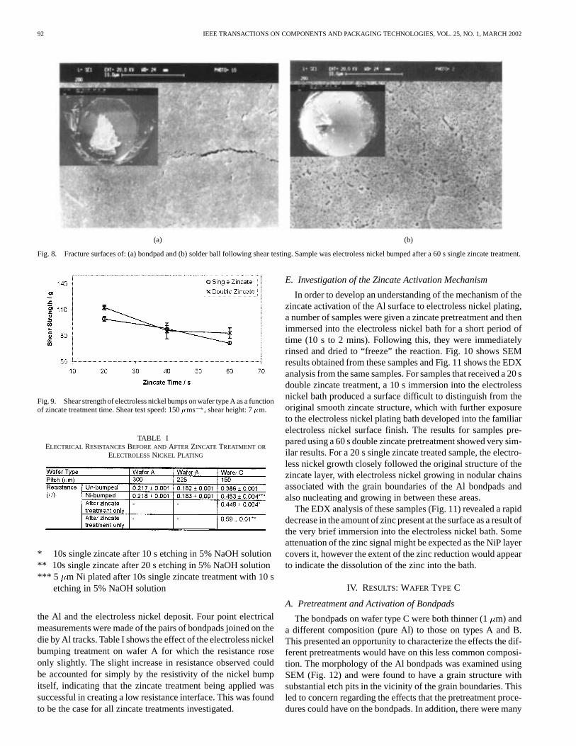
using shear testing with a range of structures. Due to difficultiesin carrying out shear tests directly on NiP bumps, initial trialswere conducted on the large BGA sized bondpads of wafer typeB, which were solder bumped by reflowing BGA solder ballsonto them. A number of these die were bumped, using a range ofzincate treatments and were then characterized by shear testing.Fig. 7 shows the results of these tests and indicates that for themajority of single and double zincate treatments the shear forcewas very similar, which could be correlated with SEM obser-vations of the fracture surface that clearly indicated that shearfailure always occurred through the solder material. The onlyexception to this was the 60 s single zincate treated sample,which exhibited reduced shear strength and where many frac-tures could be seen at the NiP–Al interface (Fig. 8).
Following these initial measurements, further experimentswere conducted to determine directly the shear strength ofthe electroless nickel bumps. These measurements need to bemade with great care, as the size and shape of the NiP bumpscan strongly influence the results. It is very difficult to testNiP bumps of only 5 m height, as the shear tool cannot gain
Fig. 6. SEM images obtained from a 20 s single zincate treated sampleshowing different surface finish to that obtained in Fig. 3(a).
Fig. 7. Shear test results as a function of zincate activation time for BGA solderballs attached to the large bondpads (580�m passivation opening) of wafer typeB. Shear speed: 250�ms , Shear height: 50�m.
purchase on the bump edge and skids over the hard materialsurface. In order to overcome this issue, early trials used thick(30 m) bumps that were deposited to create tall featuresthat could be easily engaged by the shear test tool. However,the substantial isotropic overgrowth of the nickel bump ontothe passivation surrounding the bondpad resulted in the shearstrength of the Al pad attached to the Si surface being measuredinstead of the desired NiP–Al interface. Further samples weretherefore prepared with a 15m bump height that allowedrelatively easy testing without further complications. Theseresults are presented in Fig. 9 and show a general declinein the shear strength of the interface as the zincate time isincreased. Furthermore, for a fixed zincate time, the doublezincate treatment provided a higher strength interface than thesingle treatment, in general agreement with other studies in theliterature [15]–[17], [23].
D. Electrical Resistance of Bumped Structures
The electrical resistance of daisy chained bondpads on waferA were measured before and after electroless nickel bumpingto ensure that the treatments were removing the oxide layer onthe Al surface and creating a low resistance interface between
92 IEEE TRANSACTIONS ON COMPONENTS AND PACKAGING TECHNOLOGIES, VOL. 25, NO. 1, MARCH 2002
(a) (b)
Fig. 8. Fracture surfaces of: (a) bondpad and (b) solder ball following shear testing. Sample was electroless nickel bumped after a 60 s single zincatetreatment.
Fig. 9. Shear strength of electroless nickel bumps on wafer type A as a functionof zincate treatment time. Shear test speed: 150�ms , shear height: 7�m.
TABLE IELECTRICAL RESISTANCESBEFORE ANDAFTER ZINCATE TREATMENT OR
ELECTROLESSNICKEL PLATING
* 10s single zincate after 10 s etching in 5% NaOH solution** 10s single zincate after 20 s etching in 5% NaOH solution*** 5 m Ni plated after 10s single zincate treatment with 10 s
etching in 5% NaOH solution
the Al and the electroless nickel deposit. Four point electricalmeasurements were made of the pairs of bondpads joined on thedie by Al tracks. Table I shows the effect of the electroless nickelbumping treatment on wafer A for which the resistance roseonly slightly. The slight increase in resistance observed couldbe accounted for simply by the resistivity of the nickel bumpitself, indicating that the zincate treatment being applied wassuccessful in creating a low resistance interface. This was foundto be the case for all zincate treatments investigated.
E. Investigation of the Zincate Activation Mechanism
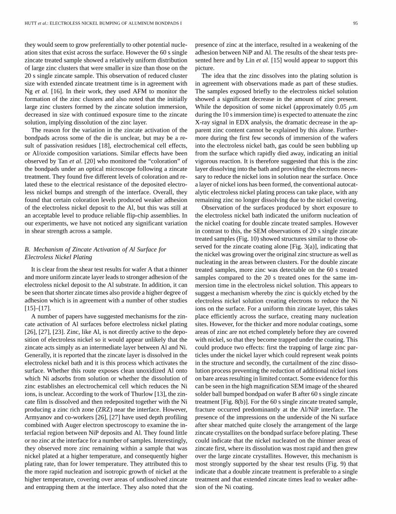
In order to develop an understanding of the mechanism of thezincate activation of the Al surface to electroless nickel plating,a number of samples were given a zincate pretreatment and thenimmersed into the electroless nickel bath for a short period oftime (10 s to 2 mins). Following this, they were immediatelyrinsed and dried to “freeze” the reaction. Fig. 10 shows SEMresults obtained from these samples and Fig. 11 shows the EDXanalysis from the same samples. For samples that received a 20 sdouble zincate treatment, a 10 s immersion into the electrolessnickel bath produced a surface difficult to distinguish from theoriginal smooth zincate structure, which with further exposureto the electroless nickel plating bath developed into the familiarelectroless nickel surface finish. The results for samples pre-pared using a 60 s double zincate pretreatment showed very sim-ilar results. For a 20 s single zincate treated sample, the electro-less nickel growth closely followed the original structure of thezincate layer, with electroless nickel growing in nodular chainsassociated with the grain boundaries of the Al bondpads andalso nucleating and growing in between these areas.
The EDX analysis of these samples (Fig. 11) revealed a rapiddecrease in the amount of zinc present at the surface as a result ofthe very brief immersion into the electroless nickel bath. Someattenuation of the zinc signal might be expected as the NiP layercovers it, however the extent of the zinc reduction would appearto indicate the dissolution of the zinc into the bath.
IV. RESULTS: WAFER TYPE C
A. Pretreatment and Activation of Bondpads
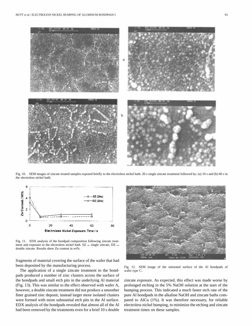
The bondpads on wafer type C were both thinner (1m) anda different composition (pure Al) to those on types A and B.This presented an opportunity to characterize the effects the dif-ferent pretreatments would have on this less common composi-tion. The morphology of the Al bondpads was examined usingSEM (Fig. 12) and were found to have a grain structure withsubstantial etch pits in the vicinity of the grain boundaries. Thisled to concern regarding the effects that the pretreatment proce-dures could have on the bondpads. In addition, there were many
HUTT et al.: ELECTROLESS NICKEL BUMPING OF ALUMINUM BONDPADS I 93
Fig. 10. SEM images of zincate treated samples exposed briefly to the electroless nickel bath. 20 s single zincate treatment followed by: (a) 10 s and (b) 60 s inthe electroless nickel bath.
Fig. 11. EDX analysis of the bondpad composition following zincate treat-ment and exposure to the electroless nickel bath. SZ= single zincate, DZ=double zincate. Results show Zn content in wt%.
fragments of material covering the surface of the wafer that hadbeen deposited by the manufacturing process.
The application of a single zincate treatment to the bond-pads produced a number of zinc clusters across the surface ofthe bondpads and small etch pits in the underlying Al material(Fig. 13). This was similar to the effect observed with wafer A,however, a double zincate treatment did not produce a smootherfiner grained zinc deposit, instead larger more isolated clusterswere formed with more substantial etch pits in the Al surface.EDX analysis of the bondpads revealed that almost all of the Alhad been removed by the treatments even for a brief 10 s double
Fig. 12. SEM image of the untreated surface of the Al bondpads ofwafer type C.
zincate exposure. As expected, this effect was made worse byprolonged etching in the 5% NaOH solution at the start of thebumping process. This indicated a much faster etch rate of thepure Al bondpads in the alkaline NaOH and zincate baths com-pared to AlCu (1%). It was therefore necessary, for reliableelectroless nickel bumping, to minimize the etching and zincatetreatment times on these samples.

94 IEEE TRANSACTIONS ON COMPONENTS AND PACKAGING TECHNOLOGIES, VOL. 25, NO. 1, MARCH 2002
(a)
(b)
Fig. 13. Zincate structure on wafer type C after: (a) single and (b) doubletreatments.
B. Adhesion of Electroless Nickel Bumps to Wafer C Bondpads
The adhesion of electroless nickel bumps plated onto thebondpads of wafer C was investigated using shear testing in thesame manner as for wafers A and B. Table II shows the resultsof these tests for samples with a variety of pretreatments. Incontrast to the results obtained for wafer A, the length of theinitial NaOH etch had a substantial effect on the shear strengthof the bumps. In particular, for a 10 s double zincate treatment,the shear strength could be more than doubled by etching withNaOH for only 10 s instead of 20 s.
C. Electrical Characterization of Electroless Nickel BumpedWafer C
Table I shows the results of four point resistance measure-ments made on pairs of bondpads linked by an Al track. Afterelectroless nickel bumping, the resistance had increased signif-icantly in contrast to the results obtained with wafer A, how-ever in order to identify whether this was entirely due to theelectroless nickel bump or another factor, results were taken forsamples at various stages of the pretreatment process. Theserevealed that the majority of the resistance change was taking
TABLE IISHEAR STRENGTH (IN GRAM FORCE) OF ELECTROLESSNICKEL BUMPS ON
WAFER TYPE C AS A FUNCTION OF ZINCATE TREATMENT TIME
place as a result of the activation steps and was strongly affectedby the NaOH etch time, leading to the conclusion that the resis-tance change was a result of the thinning of the Al pad ratherthan the incomplete removal of an oxide layer.
V. DISCUSSION
While there have been many studies in the literature regardingthe zincate activation of Al, many of them relate to the activa-tion of large engineering parts rather than small features such asAl bondpads. In addition, the studies that characterize the ad-hesion of deposits are based on a variety of electroless nickelbath formulations and zincate treatments, which could signifi-cantly influence the results. The following discussion attemptsto correlate the results of many of these studies with observa-tions made during the experiments reported here and also aimsto provide an overview of the key features of the zincate processthat influence the reliability of the bumping process.
A. Mechanism of Zincate Deposition
The mechanism of the initial zincate deposition onto the Alsurface has been described by a number of other research groups[24], [25], [11]–[14], [2], [19]. The process is a redox one in-volving the dissolution of Al metal from the surface thereby re-leasing electrons to reduce Zn ions from solution. This can besummarized by the following equations [2]:
Anodic dissolution of aluminum:
Cathodic deposition of zinc:
The SEM images of the single zincate step [Figs. 3(a) and 13] in-dicate that this process is not completely uniform and produceslarge clusters of zinc preferentially at the grain boundaries ofthe Al pad. What appears to be occurring is the dissolution ofthe Al between the grain boundaries leading to the formation ofthe pits that are visible in the background of Figs. 3(a). Thesepits persist after the Zn is etched away by the nitric acid andpresumably provide a new set of nucleation sites for the secondzincate deposition step leading to a more uniform and regulargrowth. The enhanced growth at the grain boundaries could beexpected due to the higher surface free energy of these regions,which capture the Zn atoms during deposition. Baggerman andSchwarzbach [19] suggest that this is due to a thinner aluminumoxide layer in these regions, which is broken down more rapidlythan elsewhere by the zincate solution, leading to the early nu-cleation of zinc clusters at these sites. Once these nuclei form
HUTT et al.: ELECTROLESS NICKEL BUMPING OF ALUMINUM BONDPADS I 95
they would seem to grow preferentially to other potential nucle-ation sites that exist across the surface. However the 60 s singlezincate treated sample showed a relatively uniform distributionof large zinc clusters that were smaller in size than those on the20 s single zincate sample. This observation of reduced clustersize with extended zincate treatment time is in agreement withNg et al. [16]. In their work, they used AFM to monitor theformation of the zinc clusters and also noted that the initiallylarge zinc clusters formed by the zincate solution immersion,decreased in size with continued exposure time to the zincatesolution, implying dissolution of the zinc layer.
The reason for the variation in the zincate activation of thebondpads across some of the die is unclear, but may be a re-sult of passivation residues [18], electrochemical cell effects,or Al/oxide composition variations. Similar effects have beenobserved by Tanet al. [20] who monitored the “coloration” ofthe bondpads under an optical microscope following a zincatetreatment. They found five different levels of coloration and re-lated these to the electrical resistance of the deposited electro-less nickel bumps and strength of the interface. Overall, theyfound that certain coloration levels produced weaker adhesionof the electroless nickel deposit to the Al, but this was still atan acceptable level to produce reliable flip-chip assemblies. Inour experiments, we have not noticed any significant variationin shear strength across a sample.
B. Mechanism of Zincate Activation of Al Surface forElectroless Nickel Plating
It is clear from the shear test results for wafer A that a thinnerand more uniform zincate layer leads to stronger adhesion of theelectroless nickel deposit to the Al substrate. In addition, it canbe seen that shorter zincate times also provide a higher degree ofadhesion which is in agreement with a number of other studies[15]–[17].
A number of papers have suggested mechanisms for the zin-cate activation of Al surfaces before electroless nickel plating[26], [27], [23]. Zinc, like Al, is not directly active to the depo-sition of electroless nickel so it would appear unlikely that thezincate acts simply as an intermediate layer between Al and Ni.Generally, it is reported that the zincate layer is dissolved in theelectroless nickel bath and it is this process which activates thesurface. Whether this route exposes clean unoxidized Al ontowhich Ni adsorbs from solution or whether the dissolution ofzinc establishes an electrochemical cell which reduces the Niions, is unclear. According to the work of Thurlow [13], the zin-cate film is dissolved and then redeposited together with the Niproducing a zinc rich zone (ZRZ) near the interface. However,Armyanov and co-workers [26], [27] have used depth profilingcombined with Auger electron spectroscopy to examine the in-terfacial region between NiP deposits and Al. They found littleor no zinc at the interface for a number of samples. Interestingly,they observed more zinc remaining within a sample that wasnickel plated at a higher temperature, and consequently higherplating rate, than for lower temperature. They attributed this tothe more rapid nucleation and isotropic growth of nickel at thehigher temperature, covering over areas of undissolved zincateand entrapping them at the interface. They also noted that the
presence of zinc at the interface, resulted in a weakening of theadhesion between NiP and Al. The results of the shear tests pre-sented here and by Linet al. [15] would appear to support thispicture.
The idea that the zinc dissolves into the plating solution isin agreement with observations made as part of these studies.The samples exposed briefly to the electroless nickel solutionshowed a significant decrease in the amount of zinc present.While the deposition of some nickel (approximately 0.05mduring the 10 s immersion time) is expected to attenuate the zincX-ray signal in EDX analysis, the dramatic decrease in the ap-parent zinc content cannot be explained by this alone. Further-more during the first few seconds of immersion of the wafersinto the electroless nickel bath, gas could be seen bubbling upfrom the surface which rapidly died away, indicating an initialvigorous reaction. It is therefore suggested that this is the zinclayer dissolving into the bath and providing the electrons neces-sary to reduce the nickel ions in solution near the surface. Oncea layer of nickel ions has been formed, the conventional autocat-alytic electroless nickel plating process can take place, with anyremaining zinc no longer dissolving due to the nickel covering.
Observation of the surfaces produced by short exposure tothe electroless nickel bath indicated the uniform nucleation ofthe nickel coating for double zincate treated samples. Howeverin contrast to this, the SEM observations of 20 s single zincatetreated samples (Fig. 10) showed structures similar to those ob-served for the zincate coating alone [Fig. 3(a)], indicating thatthe nickel was growing over the original zinc structure as well asnucleating in the areas between clusters. For the double zincatetreated samples, more zinc was detectable on the 60 s treatedsamples compared to the 20 s treated ones for the same im-mersion time in the electroless nickel solution. This appears tosuggest a mechanism whereby the zinc is quickly etched by theelectroless nickel solution creating electrons to reduce the Niions on the surface. For a uniform thin zincate layer, this takesplace efficiently across the surface, creating many nucleationsites. However, for the thicker and more nodular coatings, someareas of zinc are not etched completely before they are coveredwith nickel, so that they become trapped under the coating. Thiscould produce two effects: first the trapping of large zinc par-ticles under the nickel layer which could represent weak pointsin the structure and secondly, the curtailment of the zinc disso-lution process preventing the reduction of additional nickel ionson bare areas resulting in limited contact. Some evidence for thiscan be seen in the high magnification SEM image of the shearedsolder ball bumped bondpad on wafer B after 60 s single zincatetreatment [Fig. 8(b)]. For the 60 s single zincate treated sample,fracture occurred predominantly at the Al/NiP interface. Thepresence of the impressions on the underside of the Ni surfaceafter shear matched quite closely the arrangement of the largezincate crystallites on the bondpad surface before plating. Thesecould indicate that the nickel nucleated on the thinner areas ofzincate first, where its dissolution was most rapid and then grewover the large zincate crystallites. However, this mechanism ismost strongly supported by the shear test results (Fig. 9) thatindicate that a double zincate treatment is preferable to a singletreatment and that extended zincate times lead to weaker adhe-sion of the Ni coating.

96 IEEE TRANSACTIONS ON COMPONENTS AND PACKAGING TECHNOLOGIES, VOL. 25, NO. 1, MARCH 2002
It is clear from the results that for wafer type C, havingpure Al bondpads, the pretreatment regime was critical tomaintaining the structural integrity of the bondpad. The AlCu(1 wt%) pads of wafers A and B did not show significantetching by either the NaOH or zincate treatments. In addition,these pads were much thicker and would not have been asstrongly affected by the same degree of etching. Luet al. [28]studied the zincate activation of Al and AlCuSi bondpads andnoted that the AlCuSi pads etched much faster than the pureAl. In this study it was found that the Al pads etched faster thanthe AlCu ones. This difference between the two studies may beattributable to the more uneven surface morphology of thesepads to begin with. It is the high rate of etching and potential fordamage of the bondpad by the pretreatments that has promptedsome researchers to examine alternative activation proceduresthat use either modified zincate baths [29] or alternative directnickel deposition techniques [30]–[32].
Shear testing of solder bumped bondpads showed that most ofthe zincate treatment regimes used, produced sufficient adhesionto ensure that shear took place through the solder material ratherthan at the NiP–Al interface. For wafer type C, despite the severeetching of the bondpad by the pretreatments, the shear strengthcould be higher than for wafer type A. This may be a result ofthe severe pitting induced by the pretreatments that roughenedthe surface leading to more mechanical interlocking of the NiPdeposit with the bondpad. Bump pull tests would be a better wayof determining the adhesion of the NiP deposit to the Al bondpad.In particular, this type of measurement would avoid some of thebump shape and size issues that affected the shear test valuesreported above. At present there do not appear to be any studiesin the literature that report this type of measurement.
VI. CONCLUSION
The activation of Al bondpads using a zincate pretreatmenthas been investigated and compared with other data presentedin the literature. In general it was found that a short double zin-cate treatment gave the best adhesion of the electroless nickeldeposit and leads to minimal etching of the Al bondpad, whichis in agreement with data presented by other groups. The otherpretreatment steps, especially the sodium hydroxide etch, mustalso be carefully controlled to ensure that the Al bondpads arenot etched severely, which can result in weaker adhesion and in-creased electrical resistance.
The mechanism of the zincate activation process has been in-vestigated by briefly exposing zincate treated samples to theelectroless nickel bath and the results support the suggestionthat the zinc dissolves into solution releasing electrons to reducethe nickel ions, thereby creating nucleation sites on the surface.Again, the results indicate that the thinner more uniform zincatelayers produce more uniform nucleation and growth of the elec-troless nickel coating.
REFERENCES
[1] J. Liu, “Development of a cost-effective and flexible bumping methodfor flip-chip interconnections,”Hybrid Circuits, vol. 29, pp. 25–31, Sept.1992.
[2] E. Zakel and H. Reichl,Flip Chip Technologies, J. Lau, Ed. New York:McGraw-Hill, 1995, pp. 415–490.
[3] S. Wiegele, P. Thompson, R. Lee, and E. Ramsland, “Reliability andprocess characterization of electroless nickel–gold/solder flip chip in-terconnect technology,” inProc. 48th Electron. Comp. Technol. Conf.,1998, pp. 421–426.
[4] G. Motulla, P. Kasulke, K. Heinricht, A. Ostmann, E. Zakel, H. Reichl,G. Aszdasht, and J. Kloeser, “A low cost bumping process for flip chiptechnology using electroless Ni/Au bumping and solder ball placement,”Adv. Electron. Packag., vol. EEP 19-1, pp. 57–64, 1997.
[5] J. Kloeser, K. Heinricht, K. Kutzner, E. Jung, A. Ostmann, and H. Reichl,“Fine pitch stencil printing of Sn/Pb and lead free solders for flip chiptechnology,”IEEE Trans. Comp., Packag., Manufact. Technol. C, vol.21, pp. 41–49, Jan. 1998.
[6] Y. M. Chow, W. M. Lau, R. E. Schetty, and Z. S. Karim, “Feasibilityand reliability study on the electroless nickel bumping and stencilsolder printing for low cost flip chip electronic packaging,” inProc.IEEE/CPMT Int. Electron. Manufact. Technol. Symp. (IEMTS), 2000,pp. 79–84.
[7] W. Riedel,Electroless Nickel Plating. New York: Finishing Publica-tions, 1991.
[8] G. G. Gawrilov, Chemical (Electroless) Nickel-Plating. New York:Portcullis Press, 1979.
[9] T. Pearson and S. J. Wake, “Improvements in the pretreatment of alu-minum as a substrate for electrodeposition,”Trans. Inst. Met. Fin., vol.75, pp. 93–97, 1997.
[10] F. J. Monteiro and D. H. Ross, “A study of modified alloy zincate pre-treatments for plating aluminum part I,”Trans. Inst. Met. Fin., vol. 62,pp. 98–103, 1984.
[11] , “A study of modified alloy zincate pretreatments for plating alu-minum part II,”Trans. Inst. Met. Fin., vol. 62, pp. 155–159, 1984.
[12] F. J. Monteiro, M. A. Barbosa, D. H. Ross, and D. R. Gabe, “Pretreat-ments to improve the adhesion of electrodeposits on aluminum,”Surf.Interface Anal., vol. 17, pp. 519–528, 1991.
[13] K. P. Thurlow, “Electroless nickel plating on aluminum connectors,”Trans. Inst. Met. Fin., vol. 67, pp. 82–86, 1989.
[14] S. G. Robertson and I. M. Ritchie, “Role of iron (III) and tartrate in thezincate immersion process for plating aluminum,”J. Appl. Electrochem.,vol. 27, pp. 799–804, 1997.
[15] K.-L. Lin, S.-K. Chen, and S.-Y. Chang, “Adhesion of multilayer solderpads on silicon,”J. Mater. Sci.: Mater. Electron., vol. 8, pp. 253–257,1997.
[16] W.-C. Ng, T.-M. Ko, W. Chen, and G.-J. Qi, “The effects of immer-sion zincation to the electroless nickel under-bump materials in micro-electronics packaging,” inProc. IEEE/CPMT Electron. Packag. Technol.Conf., 1998, pp. 89–94.
[17] A. Ostmann, J. Kloeser, and H. Reichl, “Implementation of a chemicalwafer bumping process,” inProc. IEPS Conf., 1995, pp. 354–366.
[18] A. Ostmann, J. Simon, and H. Reichl, “The pretreatment of aluminumbondpads for electroless nickel bumping,” inProc. IEEE Multichip-Module Conf. (MCMC), 1993, pp. 74–78.
[19] A. F. J. Baggerman and D. Schwarzbach, “Solder jetted eutectic PbSnbumps for flip-chip,”IEEE Trans. Comp., Packag., Manufact. Technol.B, vol. 21, pp. 371–381, Nov. 1998.
[20] Q. Tan, C. Beddingfield, A. Mistry, and V. Mathew, “Zincation charac-terization for electroless Ni/Au UBM of solder bumping technology,”in Proc. IEEE/CPMT Int. Electron. Manufact. Technol. Symp. (IEMTS),1998, pp. 34–40.
[21] D. A. Hutt, C. Liu, P. P. Conway, D. C. Whalley, and S. H. Mannan,“Electroless nickel bumping of aluminum bondpads, part 2: Electro-less nickel plating,”IEEE Trans. Comp. Packag. Technol., vol. 25, pp.???–???, Mar. 2002.
[22] B. R. Strohmeier, W. T. Evans, and D. M. Schrall, “Preparation and sur-face characterization of zincated aluminum memory disc substrates,”J.Mater. Sci., vol. 28, pp. 1563–1572, 1993.
[23] J. Cai, S. Law, A. Teng, and P. C. H. Chan, “Influences of pad shapeand solder microstructure on shear force of low cost flip chip bumps,”in Proc. IEEE/CPMT Int. Electron. Manufact. Technol. Symp. (IEMTS),2000, pp. 91–98.
[24] S. G. Robertson, I. M. Ritchie, and D. M. Druskovic, “A kinetic andelectrochemical study of the zincate immersion process for aluminum,”J. Appl. Electrochem., vol. 25, pp. 659–666, 1995.
[25] E. Stoyanova and D. Stotchev, “Electrochemical aspects of the im-mersion treatment of aluminum,”J. Appl. Electrochem., vol. 27, pp.685–690, 1997.
[26] S. Armyanov, O. Steenhaut, N. Krasteva, J. Georgieva, J.-L. Delplancke,R. Winand, and J. Vereecken, “Auger electron spectroscopy element pro-files and interface with substrates of electroless deposited ternary al-loys,” J. Electrochem. Soc., vol. 143, pp. 3692–3698, 1996.

HUTT et al.: ELECTROLESS NICKEL BUMPING OF ALUMINUM BONDPADS I 97
[27] E. Valova, S. Armyanov, J.-L. Delplancke, R. Winand, O. Steenhaut,and J. Vereecken, “Interface with substrates of high-phosphorus electro-less NiP and NiCuP deposited from nonammonia alkaline solutions,”J.Electrochem. Soc., vol. 143, pp. 2804–2815, 1996.
[28] S.-W. Lu, R.-H. Uang, K.-C. Chen, H.-T. Hu, L.-C. Kung, and H.-C.Huang, “Fine pitch low-cost bumping for flip chip technology,” inProc.IEEE/CPMT Int. Electron. Manufact. Technol. Symp. (IEMTS), 1998,pp. 127–130.
[29] J. I. Han and S. J. Hong, “Ni electroless plating process for solder bumpchip on glass technology,”Jpn. J. Appl. Phys., vol. 36, pp. 2091–2095,1997.
[30] H. Watanabe and H. Honma, “Fabrication of nickel microbump on alu-minum using electroless nickel plating,”J. Electrochem. Soc., vol. 144,pp. 471–476, 1997.
[31] H. Honma, H. Watanabe, and T. Kobayashi, “Direct nickel plating onaluminum substrate for microbump formation,”J. Electrochem. Soc.,vol. 141, pp. 1791–1795, 1994.
[32] Q. Tan, C. Beddingfield, and A. Mistry, “Reliability evaluation of probe-before-bump technology,” inProc. IEEE/CPMT Int. Electron. Manu-fact. Technol. Symp. (IEMTS), 1999, pp. 320–324.
David A. Hutt received the B.Sc. degree in chem-istry and the Ph.D. degree in surface science fromImperial College, London, U.K., in 1988 and 1992,respectively.
He continued to study fundamental surfacechemistry physics as a Research Associate at theUniversity of Warwick, Loughborough University,U.K., and the University of Nottingham, U.K.In 1997, he joined the Interconnection Group,Loughborough University, investigating flip-chipassembly and in 1999 was appointed to a lectureship
in the same Department. His current research interests include alternativesubstrates for flip-chip assembly and fluxless soldering techniques.
Changqing Liu received the B.Eng. degree inmaterials science and engineering from NanjingUniversity of Science and Technology, China,in 1985, the M.Sc. degree in PVD films andcharacterization from the Metal Research Institute,Chinese Academy of Science, Shenyang, and thePh.D. degree from the Research Centre in SurfaceEngineering (RCSE), Hull University, U.K., in 1997.
After five years of employment in the ChineseAcademy of Science as Assistant Professor, hesecured an overseas research student scholarship.
From 1997 to 2000 he worked at the IRC in Materials, Birmingham Universityas a Postdoctoral Research Fellow. Since February 2000, as a ResearchFellow, he has been working on surface coatings for fluxless soldering andlow cost flip-chip bumping technology within the Interconnection Group,Loughborough University. He has published over 25 scientific and technicaljournal papers in materials science and engineering.
Paul P. Conwayreceived the B.S. degree (with firstclass honors) from the University of Ulster, U.K., in1988 and the M.S. degree from Loughborough, U.K.,in 1989.
He is currently a Reader in the Wolfson School ofMechanical and Manufacturing Engineering, Lough-borough University. He was a Research Assistant ona project addressing process modelling of reflow sol-dering and prior to that an Industrial Engineer withFisher Body Overseas Corp., General Motors Corpo-ration. He has held a number of substantial U.K., Eu-
ropean, and industrially funded research projects and has published widely inthe field of electronics manufacturing and micro-systems technology.
David C. Whalley received the M.S. degree fromLoughborough University, U.K., in 1984.
Since then he has been involved in researchinto electronic interconnection reliability, newinterconnection technologies such as conductiveadhesives and into the use of engineering analysistechniques both in electronic product design and forelectronic manufacturing process simulation. Thisresearch has led to the publication of over 80 peerreviewed technical papers. He is a Senior Lecturerin Loughborough University’s Wolfson School
of Mechanical and Manufacturing Engineering. He has previously workedas a Research Engineer both at Loughborough University and at the LucasAdvanced Engineering Centre, Solihull, Birmingham. He has also recentlybeen a Visiting Professor at Chalmers University, Gothenburg, Sweden, anda Visiting Researcher at NTU, Singapore, while on sabbatical leave fromLoughborough University.
Samjid H. Mannan received the M.S. degree inphysics from Oxford University, Oxford, U.K., andthe Ph.D. degree from Southampton University, U.K.
He has been working in the area of electronicsmanufacturing since 1992. After holding post-doc-toral positions at Salford and LoughboroughUniversities, he was appointed lecturer in theDepartment of Mechanical Engineering, King’sCollege, London, U.K., in 1999, and was awardedan Advanced Research Fellowship from EPSRClater that year. His current interests include flip chip
assembly, high temperature electronics, rheology, and processing of adhesivesand solder pastes.