electrical transfer, carrier concentration and surface
TRANSCRIPT

Comptes Rendus
Chimie
Umapathi Krishnamoorthy and SathishKumar Shanmugam
Electrical transfer, carrier concentration and surface charge analysis ofa single-gated cylindrical channel junctionless p-type nanowirefield-effect transistor for sensor applications
Volume 24, issue 2 (2021), p. 207-213
<https://doi.org/10.5802/crchim.75>
© Académie des sciences, Paris and the authors, 2021.Some rights reserved.
This article is licensed under theCreative Commons Attribution 4.0 International License.http://creativecommons.org/licenses/by/4.0/
Les Comptes Rendus. Chimie sont membres duCentre Mersenne pour l’édition scientifique ouverte
www.centre-mersenne.org

Comptes RendusChimie2021, 24, n 2, p. 207-213https://doi.org/10.5802/crchim.75
Full paper / Article
Electrical transfer, carrier concentration and surface
charge analysis of a single-gated cylindrical channel
junctionless p-type nanowire field-effect transistor
for sensor applications
Umapathi Krishnamoorthy∗, a and SathishKumar Shanmugama
a Department of Electrical and Electronics Engineering, M. Kumarasamy College ofEngineering, Karur, Tamilnadu, India
E-mails: [email protected] (U. Krishnamoorthy), [email protected](S. K. Shanmugam)
Abstract. The primary goal of the junctionless nanowire FET is to eliminate the struggle of makingjunctions and doping in short channel nanowire FETs. Junctions and doping are totally removed whiletaking the junctionless nanowire FET. In this work, we have modeled and analyzed various p-typejunctionless nanowire FETs without doping in junctions. The materials used in this analysis wereSilicon (Si), Germanium (Ge), Indium Phosphide (InP), Gallium Arsenide (GaAs), and Al(x)Ga(1−x)As.The dimensions of the p-type cylindrical nanowire channel were 25 nm long and 10 nm diameter.The electrical transfer studies and carrier concentration analysis are displayed. In addition, surfacecharge and potential analysis of a cylindrical channel are validated. The InP nanowire exhibits ahigher surface potential. This kind of high response surface potential can be used for the fabricationof nanostructure-based sensors.
Keywords. Electrical wire, NWFET device, Junctionless NanoWirel, Gate voltage, FET channel.
Manuscript received 23rd November 2020, accepted 11th March 2021.
1. Introduction
To obtain potential downscaling of active devicessuch as field-effect transistors (FETs), the emerg-ing of new structures and materials is extremelyneeded. Nanowire FETs have been reported as
∗Corresponding author.
promising candidates that makes this miniatur-ization possible. In one-dimensional devices suchas a nanowire, only one of the three Cartesian di-rections is much larger than the de Broglie wave-length; thus the energy spectrum is analog type inone direction and quantum confined in the othertwo dimensions. A review on Matt Law [1] of semi-conductor nanowires and nanotubes enlighten theelectronic and optical properties owing to their
ISSN (electronic) : 1878-1543 https://comptes-rendus.academie-sciences.fr/chimie/

208 Umapathi Krishnamoorthy and SathishKumar Shanmugam
unique structural one-dimensionality and possiblequantum confinement effects in two dimensions.With a broad draft of compositions and band struc-tures, these one-dimensional semiconductor nanos-tructures are considered to be the critical compo-nents in a wide range of potential nanoscale de-vice applications. One-dimensional semiconductingnanowires [2] and carbon nanotubes [3,4] are consid-ered an attractive alternative to conventional metal-oxide-semiconductor field-effect transistors (MOS-FETs) [5]. One-dimensional nanostructure of carbonnanotube (CNT) provides excellent electronic prop-erties [3,6] with reduced scattering of charge carriers.Carbon nanotubes [7] and Ge/Si nanowires [8] carriermean free path characteristics have already studied.Ballistic conduction is achieved in the carbon nan-otube FET fabrication [9]. Even if CNTs are used inmany applications, the practical difficulties of fabri-cating the uniform semiconducting nanotubes makethe requirement of other one-dimensional nanos-tructures like nanowires necessary [10]. Nanowirescan be fabricated easily due to well-established in-dustrial methodology with high electronic propertiesand easily combined with the large-scale integratedsystems [11]. The advantages and applications ofusing nanowire transistors in chemical, biochemi-cal, and biosensors [12] making the complete cur-rent flow can be blocked if a single analytic mole-cule interacting with the respective receptor on thenanowire surface was reported [13]. There is moresolicitude on the junctionless nanowire transistorand the appropriate doping concentration for thesensor and other applications [14]. The electricalcharacteristics of the junctionless nanowire transis-tors are identical to those of regular trigate MOSFETs.Practically, the fabrication of one-dimensional de-vices needs highly precise nanofabrication units andcomplex process methods. So, prior to real-time fab-rication, a systematic design and simulation is veryessential for the cognizant performance of circuitelements and devices. Junctionless nanowire tran-sistors (JNTs) feature bulk conduction as opposed tosurface conduction [15–17], making them an inter-esting candidate for nanowire (NW) FET biosensordevices with high S/V ratios. One important tech-nological goal aims at the complete integration ofa reliable heterogeneous system for which partscan better be fabricated and tested separately andcombined possibly as modular components while
operating at low powers and ambient conditions.There is tremendous potential for JNT sensors inheterogeneous nanosystems for noninvasive clinicaldiagnostics, portable, and disposable applications.Junctionless transistors can be used to improve theanalog performance of self-cascode configuration.JNT can also be used in digital electronics domain.
In this work, we have designed p-type junction-less nanowire FETs without doping in junctions. Toinvestigate the electrical transfer studies and car-rier concentration analysis, various semiconductormaterials such as Silicon (Si), Germanium (Ge), In-dium Phosphide (InP), Gallium Arsenide (GaAs), andAl(x)Ga(1−x)As are used. In addition, surface chargeand potential analysis are also studied.
2. Materials and methods
2.1. Device design and structure parameters
In this work, the cylindrical structure junctionlessnanowire channel is selected. The cylindrical struc-ture is used to make free from edges effect andto improve the short channel effects performance.The cylindrical junctionless nanowire channel is de-signed with dimensions of 25 nm length and 10 nmdiameter and having a p-type doped concentration(NA) of 1×1016 cm3. Silicon (Si), Germanium (Ge), In-dium Phosphide (InP), Gallium Arsenide (GaAs), andAl(x)Ga(1− x)As are the materials used in nanowire.This wire is placed on top of a 3 nm thick rectangularSilicon dioxide (SiO2) slab to form the FET element.The gate contact work function is achieved by ap-plying a gate terminal input potential. The SiO2 gatehas 4.1 eV work function and relative permittivityvalue of 4.2. Perfect ohmic contacts were establishedon both ends of the wire. The theoretical devicegeometry for simulation is shown in Figure 1. Fig-ure 2 shows the electrical connection of the junction-less nanowire FET. Because of the p-type nanowireFET, the gate signal having the negative bias anddrain is also having negative bias with respect tosource.
3. Results and discussions
3.1. Effect of gate voltage on drain current
The drain currents were measured by changing thenegative gate voltage from zero to 4.0 V. Variations
C. R. Chimie — 2021, 24, n 2, 207-213

Umapathi Krishnamoorthy and SathishKumar Shanmugam 209
Figure 1. Structure of NWFET device.
Figure 2. Electrical connections of junction-less NanoWire FET.
Figure 3. Characteristics of drain current withnegative gate voltage.
of drain current with biasing the negative gate volt-age from 0 to −4 V is shown in Figure 3. The mea-sured values are taken from the center point of thenanowire. The plot indicates that the values of draincurrent of indirect band gap materials are higher than
Figure 4. Characteristics of electric potentialwith negative gate voltage.
the direct band gap materials and alloy. From Fig-ure 3, Ge and Si have higher values of drain cur-rent compared with other materials. The Al(x)Ga(1−x)As semiconductor alloy has lower drain currentchanges. The electron mobility behavior attributesthe lower current in InP and higher variations in Ge.
3.2. Effect of gate voltage on electric potential
Figure 4 shows the change of internal electric poten-tial of the nanowire channel corresponding to bias-ing the negative gate voltage. The semiconductor al-loy Al(x)Ga(1−x)As nearly follow the GaAs because ofnearly same band gap value. There is a linear increaseof electric potential up to threshold voltage around−1.5 V, after which it saturates. For the same gate volt-ages, InP nanowires have higher and Ge nanowireshave lower electric potential.
3.3. Gate voltage vs. hole current density
Figure 5 shows the relationship between the log ofhole current density and the negative gate voltage.As we increased the bias voltage negatively from 0 to−4 V, log of hole current density is provided the re-lationship of linear changes, which may saturate af-ter the threshold voltage. InP nanowire FET provideshigher variations compared to all other materials. In-direct band gap materials have lower hole currentdensity variations when compared to direct band gapmaterials.
C. R. Chimie — 2021, 24, n 2, 207-213

210 Umapathi Krishnamoorthy and SathishKumar Shanmugam
Figure 5. Characteristics of gate voltage vs.hole current density.
Figure 6. Characteristics of conduction bandenergy level with the position of GaAs nanowireFET.
3.4. Conduction band and valance band energylevels
Figure 6 shows the GaAs conduction band energyrelationship with the position of the nanowire FETchannel. Initially, when applying zero gate potential,both the source and drain ends have the same po-tential and the middle of the nanowire has very lowconduction band energy (0.78 eV). When increasingthe negative gate potential, conduction band energydistribution level is increased from 1.25 V to 1.30 V,where the changes will take place. After that it maybe conducted. The energy distribution is shown inFigure 6. There is no conduction in 0 V, less con-duction in the range 1.25 V to 1.3 V, and more con-duction above 1.30 V. The same concept can be
Figure 7. Characteristics of valance band en-ergy level with the position of GaAs nanowireFET.
Figure 8. Characteristics of surface chargedensity with negative gate voltage.
applied to valance band energy level also. Figure 7shows the GaAs valance band energy relationshipwith the position of the nanowire FET channel. Thechange of the distribution takes place at −0.20 eVto −0.15 eV and the applied gate voltage is 1 V to1.5 V.
3.5. Surface charge density analysis
Figure 8 shows the dependence of surface chargedensity with increase in negative gate potential. Thedifferences in the surface charge density are higherin Germanium and lower in InP and others are inbetween. Figure 8 shows the relationship betweensurface charge density and negative gate voltage.
C. R. Chimie — 2021, 24, n 2, 207-213

Umapathi Krishnamoorthy and SathishKumar Shanmugam 211
Figure 9. Log of hole concentration @ Vg =−1 V InP nanowire FET.
Figure 10. Log of hole concentration @ Vg = 0 VInP nanowire FET.
Change of gate voltage and the variations in chargesare displayed clearly in Figure 8.
3.6. Hole concentration analysis
The 3D view of hole concentration at the negativebias of gate 1 V and 0 V of InP nanowire FET is shownin Figures 9 and 10. If zero bias is applied to the gate,the concentrations of the holes are very low as shownin blue color and when 1 V bias is applied to the gate,concentrations of holes increased, which is shownred color. It can be understood from the figures thatthe operation of FET can be achieved with a singletype of doping without junctions.
Figure 11. Characteristics of surface potentialwith negative gate voltage.
Figure 12. Characteristics of surface potentialwith negative drain voltage @ Vg = 2 V.
3.7. Surface potential analysis
Figure 11 shows the variations of surface potential re-lations with negative gate bias and Figures 12 and 13show the surface potential changes with the changeof drain voltage. Changes of surface potential can bedirectly used in electrochemical sensors. From Fig-ure 11, it is understood that direct band gap mate-rials (InP, GaAs) provide more variations when com-pared to indirect band gap materials (Ge, Si). Fromthe above results, the InP material provides morevariations compared to others.
3.8. I–V characteristics analysis
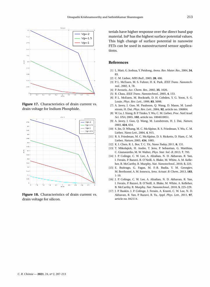
Figures 14–18 show the drain current Id relationshipwith drain voltage Vd for various channel materials.
C. R. Chimie — 2021, 24, n 2, 207-213

212 Umapathi Krishnamoorthy and SathishKumar Shanmugam
Figure 13. Characteristics of surface potentialwith negative drain voltage @ Vg = 1 V.
Figure 14. Characteristics of drain current vs.drain voltage for Al(x)Ga(1−x)As.
The change of drain current is shown in the figurefor different gate voltages like Vg for −1 V, −1.5 V, and2 V and for Vg at 2 V. Indirect band gap materials likeGermanium nanowire has taken 3.5 µA and Siliconhas taken 0.77 µA. The direct band gap materials likeGaAs has taken 0.48 µA and InP has taken 0.2 µA.The semiconductor alloy Al(x)Ga(1− x)As has taken0.25 µA.
4. Conclusion
The advantage of junctionless nanowire FET is toavoid the difficulty of making junctions and doping
Figure 15. Characteristics of drain current vs.drain voltage for GaAs.
Figure 16. Characteristics of drain current vs.drain voltage for Germanium.
in short channel nanowire FETs. In this work, we havesuccessfully modeled and analyzed various p-typejunctionless nanowire FETs without doing variousdoping in junctions. The direct and indirect semicon-ductor materials and semiconductor alloys (Si, InP,Al(x)Ga(1− x)As, GaAs, Ge) nanowire FET study hasbeen successfully done. The electrical transfer stud-ies, band gap investigations, carrier concentrationanalysis, surface charge density, and surface poten-tial studies are carried out. The indirect band gap ma-
C. R. Chimie — 2021, 24, n 2, 207-213
Umapathi Krishnamoorthy and SathishKumar Shanmugam 213
Figure 17. Characteristics of drain current vs.drain voltage for Indium Phosphide.
Figure 18. Characteristics of drain current vs.drain voltage for silicon.
terials have higher response over the direct band gapmaterial. InP has the highest surface potential values.This high change of surface potential in nanowireFETs can be used in nanostructured sensor applica-tions.
References
[1] L. Matt, G. Joshua, Y. Peidong, Annu. Rev. Mater. Res., 2004, 34,83.
[2] C. M. Lieber, MRS Bull., 2003, 28, 486.[3] P. L. McEuen, M. S. Fuhrer, H. K. Park, IEEE Trans. Nanotech-
nol., 2002, 1, 78.[4] P. Avouris, Acc. Chem. Res., 2002, 35, 1026.[5] R. Chau, IEEE Trans. Nanotechnol., 2005, 4, 153.[6] P. L. McEuen, M. Bockrath, D. H. Cobden, Y. G. Yoon, S. G.
Louie, Phys. Rev. Lett., 1999, 83, 5098.[7] A. Javey, J. Guo, M. Paulsson, Q. Wang, D. Mann, M. Lund-
strom, H. Dai, Phys. Rev. Lett., 2004, 92, article no. 106804.[8] W. Lu, J. Xiang, B. P. Timko, Y. Wu, C. M. Lieber, Proc. Natl Acad.
Sci. USA, 2005, 102, article no. 1004610051.[9] A. Javey, J. Guo, Q. Wang, M. Lundstrom, H. J. Dai, Nature,
2003, 424, 654.[10] S. Jin, D. Whang, M. C. McAlpine, R. S. Friedman, Y. Wu, C. M.
Lieber, Nano Lett., 2004, 4, 915.[11] R. S. Friedman, M. C. McAlpine, D. S. Ricketts, D. Ham, C. M.
Lieber, Nature, 2005, 434, 1085.[12] K. I. Chen, R. L. Bor, T. C. Yit, Nano Today, 2011, 6, 131.[13] T. Mikolajick, H. Andre, T. Jens, P. Sebastian, G. Matthias,
C. Gianaurelio, M. W. Walter, Phys. Stat. Sol.-R, 2013, 7, 793.[14] J. P. Colinge, C. W. Lee, A. Afzalian, N. D. Akhavan, R. Yan,
I. Ferain, P. Razavi, B. O’Neill, A. Blake, M. White, A. M. Kelle-her, B. McCarthy, R. Murphy, Nat. Nanotechnol., 2010, 5, 225.
[15] E. Buitrago, G. Fagas, M. F.-B. Badia, Y. M. Georgiev,M. Berthomé, A. M. Ionescu, Sens. Actuat. B: Chem., 2013, 183,1-10.
[16] J. P. Colinge, C. W. Lee, A. Afzalian, N. D. Akhavan, R. Yan,I. Ferain, P. Razavi, B. O’Neill, A. Blake, M. White, A. Kelleher,B. McCarthy, R. Murphy, Nat. Nanotechnol., 2010, 5, 225-229.
[17] J. P. Raskin, J. P. Colinge, I. Ferain, A. Kranti, C. W. Lee, N. D.Akhavan, R. Yan, P. Razavi, R. Yu, Appl. Phys. Lett., 2011, 97,article no. 042114.
C. R. Chimie — 2021, 24, n 2, 207-213