electrical and electronics engineering … manuals/ae/ii-i/ii-i ae manual.pdf · to make the...
TRANSCRIPT

1
ELECTRICAL AND ELECTRONICS ENGINEERING
LABORATORY MANUAL
(FOR MECH& ANE)
DEPARTMENT OF ELECTRONICS AND COMMUNICATION ENGINEERING
MALLA REDDY COLLEGE OF ENGINEERING AND TECHNOLOGY
(Sponsored by CMR Educational Society)
(Affiliated to JNTU, Hyderabad)
Secunderabad-14.

EEE LAB MANUAL MRCET
Malla Reddy College of Engineering and Technology (MRCET) Department of Mech& ANE 2
ELECTRONICS & COMMUNICATION ENGINEERING VISION To evolve into a center of excellence in Engineering Technology through creative and innovative practices in teaching-learning, promoting academic achievement & research excellence to produce internationally accepted competitive and world class professionals.
MISSION To provide high quality academic programmes, training activities, research facilities and opportunities supported by continuous industry institute interaction aimed at employability, entrepreneurship, leadership and research aptitude among students.
QUALITY POLICY Impart up-to-date knowledge to the students in Electronics & Communication
area to make them quality engineers.
Make the students experience the applications on quality equipment and
tools.
Provide systems, resources and training opportunities to achieve continuous
improvement.
Maintain global standards in education, training and services.

EEE LAB MANUAL MRCET
Malla Reddy College of Engineering and Technology (MRCET) Department of Mech& ANE 3
PROGRAMME EDUCATIONAL OBJECTIVES (PEOs)
PEO1: PROFESSIONALISM & CITIZENSHIP To create and sustain a community of learning in which students acquire knowledge and learn to apply it professionally with due consideration for ethical, ecological and economic issues. PEO2: TECHNICAL ACCOMPLISHMENTS To provide knowledge based services to satisfy the needs of society and the industry by providing hands on experience in various technologies in core field. PEO3: INVENTION, INNOVATION AND CREATIVITY To make the students to design, experiment, analyze, interpret in the core field with the help of other multi disciplinary concepts wherever applicable. PEO4: PROFESSIONAL DEVELOPMENT To educate the students to disseminate research findings with good soft skills and become a successful entrepreneur. PEO5: HUMAN RESOURCE DEVELOPMENT To graduate the students in building national capabilities in technology, education and research. PROGRAMME SPECIFIC OBJECTIVES (PSOs) PSO1 To develop a student community who acquire knowledge by ethical learning and fulfill the societal and industry needs in various technologies of core field. PSO2 To nurture the students in designing, analyzing and interpreting required in research and development with exposure in multi disciplinary technologies in order to mould them as successful industry ready engineers/entrepreneurs PSO3 To empower students with all round capabilities who will be useful in making nation strong in technology, education and research domains.

EEE LAB MANUAL MRCET
Malla Reddy College of Engineering and Technology (MRCET) Department of Mech& ANE 4
PROGRAM OUTCOMES (POs) Engineering Graduates will be able to: 1. Engineering knowledge: Apply the knowledge of mathematics, science,
engineering fundamentals, and an engineering specialization to the solution of complex engineering problems.
2. Problem analysis: Identify, formulate, review research literature, and analyze complex engineering problems reaching substantiated conclusions using first principles of mathematics, natural sciences, and engineering sciences.
3. Design / development of solutions: Design solutions for complex engineering problems and design system components or processes that meet the specified needs with appropriate consideration for the public health and safety, and the cultural, societal, and environmental considerations.
4. Conduct investigations of complex problems: Use research-based knowledge and research methods including design of experiments, analysis and interpretation of data, and synthesis of the information to provide valid conclusions.
5. Modern tool usage: Create, select, and apply appropriate techniques, resources, and modern engineering and IT tools including prediction and modeling to complex engineering activities with an understanding of the limitations.
6. The engineer and society: Apply reasoning informed by the contextual knowledge to assess societal, health, safety, legal and cultural issues and the consequent responsibilities relevant to the professional engineering practice.
7. Environment and sustainability: Understand the impact of the professional engineering solutions in societal and environmental contexts, and demonstrate the knowledge of, and need for sustainable development.
8. Ethics: Apply ethical principles and commit to professional ethics and responsibilities and norms of the engineering practice.
9. Individual and team work: Function effectively as an individual, and as a member or leader in diverse teams, and in multidisciplinary settings.
10. Communication: Communicate effectively on complex engineering activities with the engineering community and with society at large, such as, being able to comprehend and write effective reports and design documentation, make effective presentations, and give and receive clear instructions.
11. Project management and finance: Demonstrate knowledge and understanding of the engineering and management principles and apply these to one’s own work, as a member and leader in a team, to manage projects and in multi disciplinary environments.
12. Life- long learning: Recognize the need for, and have the preparation and ability to engage in independent and life-long learning in the broadest context of technological change.

EEE LAB MANUAL MRCET
Malla Reddy College of Engineering and Technology (MRCET) Department of Mech& ANE 5
Laboratory Rules
General Rules of Conduct in Laboratories: 1. You are expected to arrive on time and not depart before the end of a laboratory. 2. You must not enter a lab unless you have permission from a technician or lecturer. 3. You are expected to comply with instructions, written or oral, that the laboratory Instructor gives you during the laboratory session. 4. You should behave in an orderly fashion always in the lab. 5. You must not stand on the stools or benches in the laboratory. 6. Keep the workbench tidy and do not place coats and bags on the benches. 7. You must ensure that at the end of the laboratory session all equipment used is stored away where you found it. 8. You must put all rubbish such as paper outside in the corridor bins. Broken components should be returned to the lab technician for safe disposal. 9. You must not remove test equipment, test leads or power cables from any lab without permission. 10. Eating, smoking and drinking in the laboratories are forbidden. 11. The use of mobile phones during laboratory sessions is forbidden. 12. The use of email or messaging software for personal communications during laboratory sessions is forbidden. 13. Playing computer games in laboratories is forbidden.
Specific Safety Rules for Laboratories: 1. You must not damage or tamper with the equipment or leads. 2. You should inspect laboratory equipment for visible damage before using it. If there is a problem with a piece of equipment, report it to the technician or lecturer. DO NOT return equipment to a storage area 3. You should not work on circuits where the supply voltage exceeds 40 volts without very specific approval from your lab supervisor. If you need to work on such circuits, you should contact your supervisor for approval and instruction on how to do this safely before commencing the work. 4. Always use an appropriate stand for holding your soldering iron. 5. Turn off your soldering iron if it is unlikely to be used for more than 10 minutes. 6. Never leave a hot soldering iron unattended. 7. Never touch a soldering iron element or bit unless the iron has been disconnected from the mains and has had adequate time to cool down. 8. Never strip insulation from a wire with your teeth or a knife, always use an appropriate wire stripping tool. 9. Shield wire with your hands when cutting it with a pliers to prevent bits of wire flying about the bench.

EEE LAB MANUAL MRCET
Malla Reddy College of Engineering and Technology (MRCET) Department of Mech& ANE 6
LIST OF EXPERIMENTS
SECTION-A: ELECTRICAL ENGINEERING
S.NO EXPERIMENT NAME PAGE NO
1. MAGNETISATON CHARACTERISTICS OF D.C SHUNT GENERATOR 8-11 2. SPEED CONTROL OF D.C SHUNT MOTOR 12-15 3. SWINBURNE’S TEST ON D.C SHUNT MACHINE 16-20 4. BRAKE TEST ON D.C SHUNT MOTOR 21-24 5. OC & SC TEST ON 1-PHASE TRANSFORMER 25-31 6. BRAKE TEST ON 3-PHASE INDUCTION MOTOR 32-35 7. REGULATION OF ALTERNATOR BY SYNCHRONOUS IMEDANCE METHOD 36-39
INTRODUCTION TO ELECTRONIC DEVICES
S.NO DEVICE NAME PAGE NO
1. BASIC ELECTRONIC COMPONENETS 41-45 2. CIRCUIT SYMBOLS 46-53 3. STUDY OF CRO 54-57 4. STUDY OF FUNCTION GENERATOR 58-60 5. STUDY OF REGULATED POWER SUPPLY 61-61 6. TYPES OF CIRCUIT BOARD 62-63
SECTION-B: ELECTRONICS ENGINEERING
S.NO EXPERIMENT NAME PAGE NO
1. PN JUNCTION DIODE CHARACTERISTICS 65-68 2. ZENER DIODE CHARACTERISTICS 69-73 3. HALF WAVE RECTIFIER WITH AND WITHOUT FILTER 74-78 4. FULL WAVE RECTIFIER WITH AND WITHOUT FILTER 79-83 5. TRANSISTOR CB CHARACTERISTICS (INPUT AND OUTPUT) 84-87 6. TRANSISTOR CE CHARACTERISTICS (INPUT AND OUTPUT) 88-91

EEE LAB MANUAL MRCET
Malla Reddy College of Engineering and Technology (MRCET) Department of Mech& ANE 7
SECTION-A

EEE LAB MANUAL MRCET
Malla Reddy College of Engineering and Technology (MRCET) Department of Mech& ANE 8
1. MAGNETIZATION or OPEN CIRCUIT CHARACTERISTICS OF D.C SHUNT GENERATOR
AIM: To obtain the no load characteristics of a DC shunt generator and to determine the critical field resistance.
NAME PLATE DETAILS:
S.NO Characteristics D.C Motor D.C Generator
1 Voltage 220V 220V
2 Current 13.6A 20A
3 Speed 1500rpm 1500rpm
4 Power 5HP 3KW
APPARATUS:
S.NO Name Of The
Equipment Type Range Quantity
1 Voltmeters MC 0-300V 2NO
2 Ammeters MC 0-2A 1NO
3 Rheostats WW 370 Ω /2A 2NO
4 Tachometers Digital 0-10000rpm 1NO
CIRCUIT DIAGRAM:

EEE LAB MANUAL MRCET
Malla Reddy College of Engineering and Technology (MRCET) Department of Mech& ANE 9
THEORY: Magnetization curve is relation between the magnetizing forces and the flux density B. this is also expressed as a relation between the field current and the induced e.m.f , in a D.C machine. Varying the field current and noting corresponding values of induced e.m.f can determine this. For a self-excited machine the theoretical shape of the magnetization Curve is as shown in the figure. The induced e.m.f corresponding to residual magnetism exists when the field current is zero. Hence the curve starts, a little above the origin on y-axis. The field resistance line Rsh is a straight-line passing through the origin. If field resistance is increased so much that the resistance line does not cut the OCC at all then obviously the machine will fail to exite .If the resistance line just lies along the slope, then machine will just excite. The value of the resistance represented by the tangent to the curve is known as critical field resistance Rc for a given speed.
CRITICAL FIELD RESISTANCE: it is the resistance of the field winding of the
generator below which generator fail to build up the voltage. First OCC is plotted from the the readings then tangent is drawn to its initial position .The slope of this curve gives the critical field resistance. From the graph the critical field resistance Rc=AB/BC.
PROCEDURE: 1. Connect the circuit as per the circuit diagram shown in fig. 2. Keep the motor field rheostat Rsh at minimum position and generator field rheostat at maximum position. 3. Check that the belt on the pulley is free so that there is no load on the pulley. 4. Switch on the DPST swatch. Start the motor slowly by using starter. 5. Adjust the current so that the motor runs at its rated speed. 6. Now vary the generator field rheostat to increase the field current and take the no load voltage and field current readings. 7. Take the no load voltage values until field gets saturated. 8. Finally set the field rheostats to initial positions then switch off the supply. 9. Draw the graph between generated voltage and field current. Find the critical field resistance from the tangent line.

EEE LAB MANUAL MRCET
Malla Reddy College of Engineering and Technology (MRCET) Department of Mech& ANE 10
TABULAR COLUMN:
Residual Voltage = Speed=
SNO If(A) Eg(V)
MODEL GRAPH: Draw the graph between generated voltage at no load and field current. By taking Generated voltage Eg in volts on Y axis and field current If in amps on X-axis.
PRECAUTIONS: 1) The rheostat is connected such that minimum resistance is included in field circuit of motor. 2) The rheostat is connected such that maximum resistance is included in field circuit of generator. 3) Starter handle is moved slowly.
RESULT:

EEE LAB MANUAL MRCET
Malla Reddy College of Engineering and Technology (MRCET) Department of Mech& ANE 11
EXERCISE QUESTIONS:
VIVA QUESTIONS: 1. What is meant by critical field resistance? 2. Residual magnetism is necessary for self excited generators or not. 3. Why this test is conducted at constant speed?

EEE LAB MANUAL MRCET
Malla Reddy College of Engineering and Technology (MRCET) Department of Mech& ANE 12
5. SPEED CONTROL OF DC SHUNT MOTOR AIM: To control the speed of a DC shunt motor using the following methods i). field flux control ii). Armature voltage control
NAME PLATE DETAILS:
CHARECTERISTIC RATING
Voltage 220V
Speed 1500rpm
current 1.2A
APPARATUS: S.No NAME OF THE EQUIPMENT Type Range Qty
1 DC shunt motor DC 220V 1
2 Rheostat Wire wound 370Ω/2.5A 2
3 Ammeter MC (0-2)A 1
4 Voltmeter MC (0-220)V 1
5 Tachometer Digital (0-30000)rpm 1
CIRCUIT DIAGRAM:

EEE LAB MANUAL MRCET
Malla Reddy College of Engineering and Technology (MRCET) Department of Mech& ANE 13
THEORY: The term speed control means intentional sped variation, carried out manually or automatically. DC motors are most suitable for wide range speed control and are therefore indispensible for many adjustable speed drives. The speed of a motor is given by Wm = (Vt-IaRa)/Kaф Where Ka – armature constant = PZ/2πA And ф is the flux per pole. Hence it follows that, for a DC motor, there are basically three methods of speed control and these are:
1. Variation of resistance in armature circuit 2. Variation of the field flux 3. Variation of armature terminal voltage.
Variation of the field flux: This method of speed control, also called as flux weakening method or filed current control method gives speeds above the base speed only. Base speed is nothing but the rated speed of the machine. This is one of the simplest and economical methods and is, therefore extensively used in modern electric drives. Under steady state running conditions, if the field circuit resistance is increased, the field current and hence the field flux are reduced. Since the rotor speed cannot change suddenly due to inertia, a decrease in field current causes a reduction of counter emf. As a result of it, more current flows through armature. The percentage increase in armature current is much more than the percentage decrease in the field current. In view of this, the electromagnetic torque is increased and this being more than the load torque, the motor gets accelerated. The disadvantages of this method are:
a. The armature may get over heated at higher speeds, because the increased armature current results in more ohmic losses whereas cooling by ventilation does not improve proportionally.
b. If the field flux is weakened considerably, the speed becomes very highand due to these changes; the motor operation may become unstable.
Variation of armature terminal voltage: If the voltage applied to the armature changes the speed changes directly with it. Using this method, speeds below rated speeds are attained.
PROCEDURE:
1. Make the connections as per the circuit diagram. 2. Keep the field rheostat in minimum position and armature in maximum position
and close the DPST switch. 3. Bring the motor to rated speed using field rheostat. 4. At this point take a note of the voltmeter and tachometer readings.

EEE LAB MANUAL MRCET
Malla Reddy College of Engineering and Technology (MRCET) Department of Mech& ANE 14
5. Now start varying the armature rheostat in steps and for each step note down the voltmeter and tachometer readings. Take 10 to 15 such readings and bring back the armature rheostat to initial position.
6. Bring back the field rheostat to initial position. Using the armature rheostat set the motor at rated speed.
7. Vary the field rheostat in steps and for each step note down the ammeter and tachometer readings. Take 10 to 15 such readings.
8. Set both the rheostats to their initial positions and open the DPST switch.
TABULAR COLUMN: Armature voltage control:
S.No Va(Armature Voltage(volts))
N(Speed(rpm))
Field Flux Control:
S.No If(Field current(amperes))
N (Speed(rpm))
MODEL GRAPHS: Armature Voltage Control:

EEE LAB MANUAL MRCET
Malla Reddy College of Engineering and Technology (MRCET) Department of Mech& ANE 15
Field Flux Control:
PRECAUTIONS: 1. We should start the motor under no load 2. Take the reading without parallax error. 3. The connections must be tight.
RESULT: EXERCISE QUESTIONS:
1.A 500 V shunt motor runs at its normal speed of 250 r.p.m. when the armature current is 200 A. The resistance of armature is 0.12 ohm. Calculate the speed when a resistance is inserted in the field reducing the shunt field to 80% of normal value and the armature current is 100 ampere VIVA QUESTIONS:
1. What are the three methods of speed control? 2. What is the main purpose of speed control? 3. Why is three point starters not used in this circuit? 4. What is the method opted to get speeds above rated speed? 5. How is flux per pole related to the speed of the machine?

EEE LAB MANUAL MRCET
Malla Reddy College of Engineering and Technology (MRCET) Department of Mech& ANE 16
3. SWINBURNE’S TEST ON D.C SHUNT MACHINE
AIM: To perform Swinburne’s test on the given D.C machine and predetermine the
efficiency at any desired load both as motor and as generator.
NAME PLATE DETAILS:
S.NO Characteristic D.C Motor
1 Voltage 220V
2 Current 20A
3 Speed 1500rpm
4 Power 5HP
APPARATUS REQUIRED: S.NO Name Of The Equipment Type Range Quantity
1 Ammeter MC 0-2A,0-1A,0-10A 3NO
2 Voltmeter MC 0-30V,0-300V 2NO
3 Rheostat WW 370 Ω /2A 1NO
4 Tachometer Digital 1000rpm 1NO
CIRCUIT DIAGRAM:

EEE LAB MANUAL MRCET
Malla Reddy College of Engineering and Technology (MRCET) Department of Mech& ANE 17
CIRCUIT DIAGRAM TO FIND ARMATURE RESISTANCE:
THEORY: This test is to find out the efficiency of the machine .It is a simple indirect method in which losses are determined separately and from their knowledge, efficiency at any desired load can be predetermined. The only test needed is no-load test. This test cannot be performed on DC series motor. The machine is run as a no load shunt motor at rated speed and with a rated terminal voltage .However, this test is applicable to those machines in which flux is practically constant. The constant losses in a dc shunt machine= Wc = stray losses (magnetic & mechanical losses) +shunt field copper losses.
Wc = No load input – No load armature copper losses = VIL0 – I2
aoRa where Ra is the armature resistance And Iao=IL-Ish
PROCEDURE: 1) Make all the connections are as per the circuit diagram. 2) Keep the field rheostat in minimum resistance position. 3) Excite the motor with 220V, DC supply by closing the DPST switch and start the Motor by moving the handle of 3-point starter from OFF to ON position. 4) By adjusting the rheostat in motor field bring the speed of the motor to its rated value. Note down the readings of Ammeter and Voltmeter at no load condition. 5) The necessary calculations to find efficiency of machine as motor & generator at any given value of armature current is done.
TO FIND ARMATURE RESISTANCE (Ra): 1) Connect the circuit per the circuit diagram 2) Keep the rheostat in maximum position. 3) Now excite the motor terminals by 30V supply by closing DPST switch. 4) Note down the readings of Ammeter and voltmeter.

EEE LAB MANUAL MRCET
Malla Reddy College of Engineering and Technology (MRCET) Department of Mech& ANE 18
MODEL CALCULATIONS:- For motor: IL= Ia+If
No load losses = Wo =VIo – I2aoRa
Input = VI Cu losses = Ia
2Ra Total losses =No load losses + cu losses Output = Input-Total losses %Efficiency (η) = (Output / Input)*100
For generator: Ia = IL +If
No load losses = Wo = V Io – I2aoRa
Output = VI Cu losses = Ia2 Ra Total losses =No load losses + cu losses Input =Output+ Total losses %Efficiency (η) = (Output / Input)*100
TABULAR COLOUMN:
S.NO Voltmeter
reading V in Volts
Ammeter Reading
I in Amps
Ammeter reading
Ishin Amps
Speed in RPM
ARMATURE RESISTANCE (Ra):
S.No Voltage Current

EEE LAB MANUAL MRCET
Malla Reddy College of Engineering and Technology (MRCET) Department of Mech& ANE 19
CALCULATION TABLE: As a Motor: S.NO IL ( A) Ia=(IL-Ish) in A W=Ia
2Ra in
watts Total losses
%Efficiency
As a Generator:
S.NO IL (A) Ia=(IL+Ish) in A
W=Ia2Ra
in watts Total losses
%Efficiency
MODEL GRAPH:
PRECAUTIONS: 1. We should start the motor under no load 2. Take the reading without parallax error. 3. The connections must be tight.
RESULT:

EEE LAB MANUAL MRCET
Malla Reddy College of Engineering and Technology (MRCET) Department of Mech& ANE 20
EXERCISE QUESTIONS: 1. A 220v dc shunt motor at no load takes a current of 2.5A. The resistances of armature and shunt field are 0.8 Ω and 200Ω respectively. Estimate the efficiency of the motor when the input current is 20A. State precisely assumptions made
VIVA QUESTIONS: 1. Why the magnetic losses calculated by this method are less than the actual value? 2. Is it applied to D.C series machines? 3. Comment on the efficiency determined by this method.

EEE LAB MANUAL MRCET
Malla Reddy College of Engineering and Technology (MRCET) Department of Mech& ANE 21
4. BRAKE TEST ON D.C SHUNT MOTOR AIM: To conduct the brake test on a D.C shunt motor and to draw its performance curves.
NAME PLATE DETAILS:
S.NO Characteristic D.C Motor
1 Voltage 220V
2 Current 20A
3 Speed 1500rpm
4 Power 5HP
APPARATUS REQUIRED:
S.NO Description Type Range Quantity
1 Ammeter MC 0-20A 1NO
2 Voltmeter MC 0-300V 1NO
3 Rheostat WW 370 Ω /2A 1NO
4 Tachometer Digital 0-10000rpm 1NO
CIRCUIT DIAGRAM:
EEE LAB MANUAL MRCET
Malla Reddy College of Engineering and Technology (MRCET) Department of Mech& ANE 22
THEORY: This test is direct test to find the efficiency of the DC shunt motor. In this test the motor directly loaded by connecting brakes which are with pulley and motor is subjected to rated load and entire power is wasted. belt around the water cooled pulley has its ends attached to spring balances S1and S2.The belt tightening hand wheels h1 and h2 help in adjusting the load on the pulley so that the load on the motor can be varied.
Output power of the motor = (S1-S2)*Re*9.81*w (watts) S1, S2 = weights on the pulley. Re= Effective radius of the pulley. w=motor speed in rad/sec. If V is the terminal voltage IL is the line current Power in put =V*IL watts. Efficiency (%η)=(w(S1-S2)*Re*9.81/V*IL)*100
PROCEDURE: 1. All the connections are as per the circuit diagram. 2. 220V, DC supply is given to the motor by closing DPST switch. 3. Move the 3-point starter handle form ‘OFF’ to ‘ON’ position slowly and motor starts running. 4. Vary the field rheostat until the motor reaches its rated Speed and take voltmeter and ammeter readings. 5. Apply the land by break drum pulley and for each applications of load the Corresponding Voltmeter (V), Ammeter (I), spring forces S1 & S2 and Speed (N) Readings are noted. 6. Calculate output & efficiency for each reading. 7. Note down all the readings in the tabular form carefully. 8. Remove the load slowly and keep the rheostat as starting position and switch ‘OFF’ the supply by using DPST switch.

EEE LAB MANUAL MRCET
Malla Reddy College of Engineering and Technology (MRCET) Department of Mech& ANE 23
TABULAR COLUMN:
GRAPH: The graph is drawn between a) Output in Watts Vs Speed(N) in RPM b) Output in Watts Vs Torque (T) in N-m c) Output in Watts Vs Current (I) in A d) Output in Watts Vs Efficiency (%η) By taking output in Watts on X axis and speed, Torque, current, Efficiency onY- axis .
S. NO Voltage (V)
Current (A)
Input =VI watts
Forces in KG S1 S2
Net force F = S1~S2 in kg
Torque(T) =F*Re*9.81 (N-M)
Speed in RPM (N)
O/p= 2πNT/60 (Watts)
%Efficiency η=output/input
1 2 3 4 5 6 7

EEE LAB MANUAL MRCET
Malla Reddy College of Engineering and Technology (MRCET) Department of Mech& ANE 24
PRECAUTIONS: 1. Initially 3-point starter should be kept at ‘OFF’ position and later it must be varied slowly and uniformly from ‘OFF’ to ‘ON’ position. 2. The field regulator must be kept at its minimum output position. 3. The brake drum of the motor should filled with cold water. 4. The motor should be started without load.
RESULT: EXERCISE QUESTIONS: 1. In a brake test the effective load on the branch pulley was 38.1kg, the effective diameter of the pulley 63.5cm and speed 12 r.p.s. the motor took 49A at 220V. Calculate the output power and the efficiency at this load
VIVA QUESTIONS: 1 .Why a 3-point starter is used for starting a D.C shunt motor? 2. If a 3-point starter is not available, how can a D.C motor be started? 3. Explain the function of overload release coil in 3-point starter

EEE LAB MANUAL MRCET
Malla Reddy College of Engineering and Technology (MRCET) Department of Mech& ANE 25
5. OC & SC TESTS ON 1 – PHASE TRANSFORMER AIM:
To conduct Open circuit and Short circuit tests on 1-phase transformer to pre-determine the efficiency, regulation and equivalent parameters.
NAME PLATE DETAILS:
Voltage Ratio 220/110V
Full load Current 13.6A
KVA RATING 3KVA
APPARATUS: S.NO Description Type Range Quantity
1 Ammeter MI 0-20A 0-5A
2NO
2 Voltmeter MI 0-150V 0-300V
2NO
3 Wattmeter LPF UPF
2A,!50V 20A,300V
2NO
4 Auto
transformer - 230/0-270V 1NO
5 Transformer - 220V/110V 1NO
CIRCUIT DIAGRAM: OPEN CIRCUIT TEST:

EEE LAB MANUAL MRCET
Malla Reddy College of Engineering and Technology (MRCET) Department of Mech& ANE 26
SHORT CIRCUIT TEST:
THEORY:
Transformer is a device which transforms the energy from one circuit to other circuit without change of frequency. The performance of any transformer calculated by conducting tests .OC and SC tests are conducted on transformer to find the efficiency and regulation of the transformer at any desired power factor.
OC TEST: The objectives of OC test are 1. To find out the constant losses or iron losses of the transformer. 2. To find out the no load equivalent parameters.
SC TEST: The objectives of OC test are 1. To find out the variable losses or copper losses of the transformer. 2. To find out the short circuit equivalent parameters. By calculating the losses and equivalent parameters from the above tests the efficiency and regulation can be calculated at any desired power factor.
PROCEDURE (OC TEST): 1. Connections are made as per the circuit diagram 2. Initially variac should be kept in its minimum position 3. Close the DPST switch.

EEE LAB MANUAL MRCET
Malla Reddy College of Engineering and Technology (MRCET) Department of Mech& ANE 27
4. By varying Auto transformer bring the voltage to rated voltage 5. When the voltage in the voltmeter is equal to the rated voltage of HV winding note down all the readings of the meters. 6. After taking all the readings bring the variac to its minimum position 7. Now switch off the supply by opening the DPST switch.
PROCEDURE (SC TEST): 1. Connections are made as per the circuit diagram. 2. Short the LV side and connect the meters on HV side. 3. Before taking the single phase, 230 V, 50 Hz supply the variac should be in minimum position. 4. Now close the DPST switch so that the supply is given to the transformer. 5. By varying the variac when the ammeter shows the rated current (i.e. 13.6A) then note down all the readings. 6. Bring the variac to minimum position after taking the readings and switch off the supply.
O.C TEST OBSERVATIONS:
S.NO V0(VOLTS) I0(AMPS) W0(watts)
S.C TEST OBSERVATIONS:
S.NO VSC(VOLTS) ISC(AMPS) WSC(watts)

EEE LAB MANUAL MRCET
Malla Reddy College of Engineering and Technology (MRCET) Department of Mech& ANE 28
CALCULATIONS: (a)Calculation of Equivalent circuit parameters: Let the transformer be the step down transformer.
b) Calculation to find Efficiency
Where ‘n’ represents % of full load.

EEE LAB MANUAL MRCET
Malla Reddy College of Engineering and Technology (MRCET) Department of Mech& ANE 29
TABULAR COLUMN:
S.NO % OF LOAD EFFICIENCY
1 2 3 4 5
12.5 25 50 75 100
TABULAR COLUMN:
LAGGING POWER FACTOR LEADING POWER FACTOR
SNO PF %REG SNO PF %REG
1 0.2 1 0.2
2 0.3 2 0.3
3 0.4 3 0.4
4 0.5 4 0.5
5 0.6 5 0.6
6 0.7 6 0.7
7 0.8 7 0.8
8 0.9 8 0.9
9 UNITY 9 UNITY
EEE LAB MANUAL MRCET
Malla Reddy College of Engineering and Technology (MRCET) Department of Mech& ANE 30
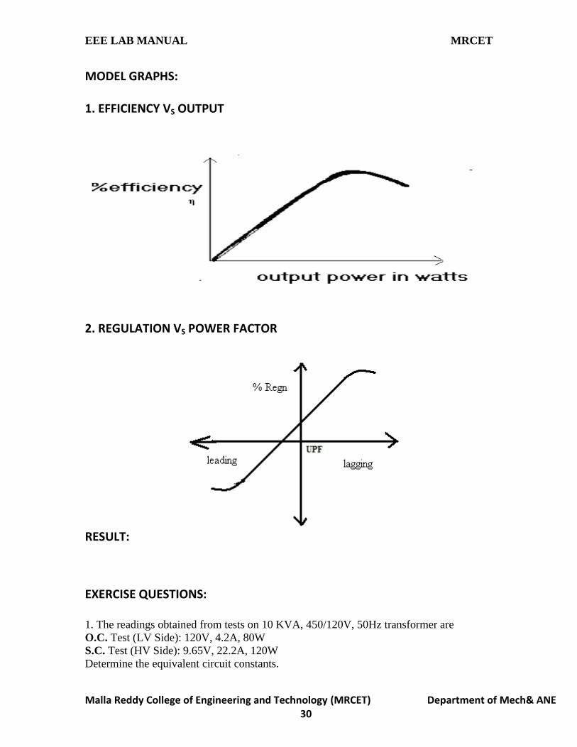
MODEL GRAPHS: 1. EFFICIENCY VS OUTPUT
2. REGULATION VS POWER FACTOR
RESULT:
EXERCISE QUESTIONS: 1. The readings obtained from tests on 10 KVA, 450/120V, 50Hz transformer are
O.C. Test (LV Side): 120V, 4.2A, 80W
S.C. Test (HV Side): 9.65V, 22.2A, 120W
Determine the equivalent circuit constants.

EEE LAB MANUAL MRCET
Malla Reddy College of Engineering and Technology (MRCET) Department of Mech& ANE 31
VIVQUESTIONS: 1) What is a transformer? 2) Draw the equivalent circuit of transformer? 3) What is the efficiency and regulation of transformer?

EEE LAB MANUAL MRCET
Malla Reddy College of Engineering and Technology (MRCET) Department of Mech& ANE 32
6. BRAKE TEST ON 3 -PHASE INDUCTION MOTOR AIM: To perform Brake test on 3- phase induction motor to determine performance characteristics.
NAME PLATE DETAILS: CHARECTERISTIC RATING
Voltage 415V
Current 7.46A
Power 5HP
Speed 1500rpm
Frequency 50Hz
APPARATUS: S.NO NAME OF THE EQUIPMENT Type Range Quantity
1 Ammeter MI 0-20A 1
2 Voltmeter MI 0-150V 0-300V
2
3 Wattmeter LPF UPF
1/2A,!50V 5/10A,300V
2
CIRCUIT DIAGRAM:
EEE LAB MANUAL MRCET
Malla Reddy College of Engineering and Technology (MRCET) Department of Mech& ANE 33
THEORY: It is the direct method to find the efficiency of the induction motor. In this test the breaking of the rotor is done with the help of the belt which surrounds the pulley by using spring balances. When the braking power is increased by tightening the springs then the line current is increased so the Force on pulley (F) = (S1-S2)*9.81 (N) Torque (T) =Force (F)* Re. N-m Output power of the motor = (S1-S2)*Re*9.81*W (watts) W=2πN/60. S1, S2 = weights on the pulley. Re= Effective radius of the pulley. W=motor speed in rad/sec. If V is the terminal voltage IL is the line current and cosΦ is the power factor.
Power in put = V*IL* cosΦ watts.
Efficiency (%η)=(w(S1-S2)*Re*9.81/ V*IL*cosΦ)*100 %slip=(Ns –N)/Ns Where Ns is the synchronous speed and N is the speed of the motor.
PROCEDURE: 1. Connect the circuit as per the circuit diagram. 2. Observing precautions close the TPST switch. 3. Apply he rated voltage to the stator windings of 3 Phase induction motor with the help of starter. 4. Note down the readings of all meters on no-load. 5. Load the induction motor in steps using the brake-drum arrangement. At each step note down the readings of all meters up to full load of the motor. 6. Gradually release the load and switch OFF the supply. 7. Using thread, measure the circumference of the brake-drum when motor is at rest.

EEE LAB MANUAL MRCET
Malla Reddy College of Engineering and Technology (MRCET) Department of Mech& ANE 34
TABULAR COLUMN:
MODEL GRAPHS: 1. Output Vs Efficiency 2. Output Vs Torque 3. Slip Vs Torque
Mechanical Characteristics

EEE LAB MANUAL MRCET
Malla Reddy College of Engineering and Technology (MRCET) Department of Mech& ANE 35
Performance Characteristics
RESULT: EXERCISE QUESTIONS:
1. A 6 pole 3φ induction motor develops 30hp including 2 hp mechanical losses at a speed of 950 r.p.m. on 550V, 50Hz Mains. The P.F. is 0.88 lagging. Find: 1) Slip 2) Rotor Cu loss 3) Total input if stator losses are 2kw 4) η 5) Line current
VIVA QUESTIONS:
1) What is motor? 2) Why test is conducted on motor? 3) What is brake test and what is the disadvantage of brake test?

EEE LAB MANUAL MRCET
Malla Reddy College of Engineering and Technology (MRCET) Department of Mech& ANE 36
7. REGULATION OF ALTERNATOR BY SYNCHRONOUS IMPEDANCE METHOD AIM: To predetermine the regulation of 3-phase alternator by using synchronous
impedance method by conducting O.C and S.C tests.
NAME PLATE DETAILS: CHARACTERISTIC DC MOTOR ALTERNATOR
Voltage 220V 415V
Current 20A 7.2A
Power 5HP 3KVA
Speed 1500rpm 1500rpm
Frequency - 50Hz
APPARATUS REQUIRED:
S.No NAME OF THE EQUIPMENT RANGE TYPE QUANTITY
1
Voltmeter AC
0-500V MI 1
2
Ammeter AC 0-10A MI 1
3 Voltmeter DC
0-300V MC 1
4 Ammeter DC 0-20A MC 2
5 RPM Meter --- DIGITAL 1
6 Connecting wires --- --- Required

EEE LAB MANUAL MRCET
Malla Reddy College of Engineering and Technology (MRCET) Department of Mech& ANE 37
CIRCUIT DIAGRAM; OC &SC TEST:
TO FIND ARMATURE RESISTANCE:
Procedure: 1.OC test: i)Connections are made as shown in the given circuit diagram for OC and SC test. ii)With the rectifier in the zero voltage position TPST switch open and the rheostat in their proper position,the dc supply to the motor is switched ON. iii)The dc motor is brought to rated speed of the alternator by properly varying the field rheostat by motor. iv)Now the alternator field is exited by applying the dc voltage through the rectifier in steps.At each step,note down the field current and corresponding generated voltage.This procedure is repeated till the voltage generated is much beyond rated value v)Reduce the alternator field excitation to zero level

EEE LAB MANUAL MRCET
Malla Reddy College of Engineering and Technology (MRCET) Department of Mech& ANE 38
2.SC test: i)With the rectifier in the minimum voltage position the TPST switch is closed. ii)Increase field excitation gradually till the SC current of the alternator reaches the rated current of alternator iii)Notedown all the meter readings

EEE LAB MANUAL MRCET
Malla Reddy College of Engineering and Technology (MRCET) Department of Mech& ANE 39
RESULT: EXERCISE QUESTIONS: 1. A 1200KV, 6600V, 3phase star connected alternator has its armature resistance as 0.25Ω per phase and its synchronous reactance as 5Ω per phase. Calculate its regulation if it delivers a full load at i) 0.8 lagging and ii) 0.8 leading power factor.
VIVA QUESTIONS:
1) What is alternator and what is regulation?
2) How we can determine the regulation by using synchronous impedance method?
EEE LAB MANUAL MRCET
Malla Reddy College of Engineering and Technology (MRCET) Department of Mech& ANE 40
INTRODUCTION TO
ELECTRONIC DEVICES

EEE LAB MANUAL MRCET
Malla Reddy College of Engineering and Technology (MRCET) Department of Mech& ANE 41
1. BASIC ELECTRONIC COMPONENTS
1.1. COLOUR CODING OF RESISTOR:
Colour Codes are used to identify the value of resistor. The numbers to the Colour are identified in the following sequence which is remembered as BBROY GREAT BRITAN VERY GOOD WIFE (BBROYGBVGW) and their assignment is listed in following table.
Black Brown Red Orange Yellow Green Blue Violet Grey White
0 1 2 3 4 5 6 7 8 9
Table1: Colour codes of resistor
First find the tolerance band, it will typically be gold ( 5%) and sometimes silver (10%).
Starting from the other end, identify the first band - write down the number associated with that color
Now read the next color, so write down a its vale next to the first value.
Now read the third or 'multiplier exponent' band and write down that as the number of zeros.
If the 'multiplier exponent' band is Gold move the decimal point one to the left. If the 'multiplier exponent' band is Silver move the decimal point two places to the left. If the resistor has one more band past the tolerance band it is a quality band.
Read the number as the '% Failure rate per 1000 hour' This is rated assuming full wattage being applied to the resistors. (To get better failure rates, resistors are typically specified to have twice the needed wattage dissipation that the circuit produces). Some resistors use this band for temco information. 1% resistors have three bands to read digits to the left of the multiplier. They have a different temperature coefficient in order to provide the 1% tolerance. At 1% the temperature coefficient starts to become an important factor. at +/-200 ppm a change in temperature of 25 Deg C causes a value change of up to 1%
Table2: procedure to find the value of resistor using Colour codes
1.2. COLOUR CODING OF CAPACITORS
An electrical device capable of storing electrical energy. In general, a capacitor consists of two metal plates insulated from each other by a dielectric. The capacitance of a capacitor depends primarily upon its shape and size and upon the relative permittivity εr of the medium between the plates. In vacuum, in air, and in most gases, εr ranges from one to several hundred..

EEE LAB MANUAL MRCET
Malla Reddy College of Engineering and Technology (MRCET) Department of Mech& ANE 42
One classification of capacitors comes from the physical state of their dielectrics, which may be gas (or vacuum), liquid, solid, or a combination of these. Each of these classifications may be subdivided according to the specific dielectric used. Capacitors may be further classified by their ability to be used in alternating-current (ac) or direct-current (dc) circuits with various current levels.
Capacitor Identification Codes: There are no international agreements in place to standardize capacitor identification. Most plastic film types (Figure1) have printed values and are normally in microfarads or if the symbol is n, Nanofarads. Working voltage is easily identified. Tolerances are upper case letters: M = 20%, K = 10%, J = 5%, H = 2.5% and F = ± 1pF.
Figure 1: Plastic Film Types
A more difficult scheme is shown in Figure 2 where K is used for indicating Picofarads. The unit is picofarads and the third number is a multiplier. A capacitor coded 474K63 means 47 × 10000 pF which is equivalent to 470000 pF or 0.47 microfarads. K indicates 10% tolerance. 50, 63 and 100 are working volts.
Figure 2: Pico farads Representation

EEE LAB MANUAL MRCET
Malla Reddy College of Engineering and Technology (MRCET) Department of Mech& ANE 43
Ceramic disk capacitors have many marking schemes. Capacitance, tolerance, working voltage and temperature coefficient may be found. which is as shown in figure 3. Capacitance values are given as number without any identification as to units. (uF, nF, pF) Whole numbers usually indicate pF and decimal numbers such as 0.1 or 0.47 are microfarads. Odd looking numbers such as 473 is the previously explained system and means 47 nF.
Figure3: ceramic Disk capacitor
Figure 4 shows some other miscellaneous schemes.
Figure 4: miscellaneous schemes.
Electrolytic capacitor properties There are a number of parameters of importance beyond the basic capacitance and capacitive reactance when using electrolytic capacitors. When designing circuits using electrolytic capacitors it is necessary to take these additional parameters into consideration for some designs, and to be aware of them when using electrolytic capacitors

EEE LAB MANUAL MRCET
Malla Reddy College of Engineering and Technology (MRCET) Department of Mech& ANE 44
ESR Equivalent series resistance: Electrolytic capacitors are often used in circuits
where current levels are relatively high. Also under some circumstances and current sourced from them needs to have low source impedance, for example when the capacitor is being used in a power supply circuit as a reservoir capacitor. Under these conditions it is necessary to consult the manufacturers’ datasheets to discover whether the electrolytic capacitor chosen will meet the requirements for the circuit. If the ESR is high, then it will not be able to deliver the required amount of current in the circuit, without a voltage drop resulting from the ESR which will be seen as a source resistance.
Frequency response: One of the problems with electrolytic capacitors is that they
have a limited frequency response. It is found that their ESR rises with frequency and this generally limits their use to frequencies below about 100 kHz. This is particularly true for large capacitors, and even the smaller electrolytic capacitors should not be relied upon at high frequencies. To gain exact details it is necessary to consult the manufacturer’s data for a given part.
Leakage: Although electrolytic capacitors have much higher levels of capacitance for
a given volume than most other capacitor technologies, they can also have a higher level of leakage. This is not a problem for most applications, such as when they are used in power supplies. However under some circumstances they are not suitable. For example they should not be used around the input circuitry of an operational amplifier. Here even a small amount of leakage can cause problems because of the high input impedance levels of the op-amp. It is also worth noting that the levels of leakage are considerably higher in the reverse direction.
Ripple current: When using electrolytic capacitors in high current applications such
as the reservoir capacitor of a power supply, it is necessary to consider the ripple current it is likely to experience. Capacitors have a maximum ripple current they can supply. Above this they can become too hot which will reduce their life. In extreme cases it can cause the capacitor to fail. Accordingly it is necessary to calculate the expected ripple current and check that it is within the manufacturer’s maximum ratings.
Tolerance: Electrolytic capacitors have a very wide tolerance. Typically this may be -
50% + 100%. This is not normally a problem in applications such as decoupling or power supply smoothing, etc. However they should not be used in circuits where the exact value is of importance.
Polarization: Unlike many other types of capacitor, electrolytic capacitors are
polarized and must be connected within a circuit so that they only see a voltage across them in a particular way.
The physical appearance of electrolytic capacitor is as shown in Figure 5.The capacitors themselves are marked so that polarity can easily be seen. In addition to this it is common for the can of the capacitor to be connected to the negative terminal.
Figure 5: Electrolytic capacitor

EEE LAB MANUAL MRCET
Malla Reddy College of Engineering and Technology (MRCET) Department of Mech& ANE 45
It is absolutely necessary to ensure that any electrolytic capacitors are connected within a circuit with the correct polarity. A reverse bias voltage will cause the centre oxide layer forming the dielectric to be destroyed as a result of electrochemical reduction. If this occurs a short circuit will appear and excessive current can cause the capacitor to become very hot. If this occurs the component may leak the electrolyte, but under some circumstances they can explode. As this is not uncommon, it is very wise to take precautions and ensure the capacitor is fitted correctly, especially in applications where high current capability exists.
1.3. COLOUR CODING OF INDUCTORS
Inductor is just coil wound which provides more reactance for high frequencies and low reactance for low frequencies. Molded inductors follow the same scheme except the units are usually micro henries. A brown-black-red inductor is most likely a 1000 uH. Sometimes a silver or gold band is used as a decimal point. So a red-gold-violet inductor would be a 2.7 uH. Also expect to see a wide silver or gold band before the first value band and a thin tolerance band at the end. The typical Colour codes and their values are shown in Figure 6.
1000uH (1millihenry), 2%
6.8 uH, 5%
Figure 6: Typical inductors Colour coding and their values.

EEE LAB MANUAL MRCET
Malla Reddy College of Engineering and Technology (MRCET) Department of Mech& ANE 46
2. CIRCUIT SYMBOLS
WIRES AND CONNECTIONS
S.NO. COMPONENT NAME CIRCUIT SYMBOL FUNCTION
1 WIRE
To pass current very easily from one part of a circuit to another.
2 WIRES JOINED
A 'blob' should be drawn where wires are connected (joined), but it is sometimes omitted. Wires connected at 'crossroads' should be staggered slightly to form two T-junctions, as shown on the right.
3 WIRES NOT JOINED
In complex diagrams it is often necessary to draw wires crossing even though they are not connected. I prefer the 'bridge' symbol shown on the right because the simple crossing on the left may be misread as a join where you have forgotten to add a 'blob'.
POWER SUPPLIES
S.NO COMPONENT NAME CIRCUIT SYMBOL FUNCTION
1. CELL
Supplies electrical energy. The larger terminal (on the left) is positive (+). A single cell is often called a battery, but strictly a battery is two or more cells joined together
2. BATTERY
Supplies electrical energy. A battery is more than one cell. The larger terminal (on the left) is positive (+).
3. DC SUPPLY
Supplies electrical energy. DC = Direct Current, always flowing in one direction.

EEE LAB MANUAL MRCET
Malla Reddy College of Engineering and Technology (MRCET) Department of Mech& ANE 47
4. AC SUPPLY
Supplies electrical energy. AC = Alternating Current, continually changing direction.
5. FUSE
A safety device which will 'blow' (melt) if the current flowing through it exceeds a specified value.
6. TRANSFORMER
Two coils of wire linked by an iron core. Transformers are used to step up (increase) and step down (decrease) AC voltages. Energy is transferred between the coils by the magnetic field in the core. There is no electrical connection between the coils.
7. EARTH(GROUND)
A connection to earth. For many electronic circuits this is the 0V (zero volts) of the power supply, but for mains electricity and some radio circuits it really means the earth. It is also known as ground.
Output Devices: Lamps, Heater, Motor, etc.
S.NO COMPONENT NAME CIRCUIT SYMBOL FUNCTION
1. LAMP(LIGHTING)
A transducer which converts electrical energy to light. This symbol is used for a lamp providing illumination, for example a car headlamp or torch bulb
2. LAMP(INDICATOR)
A transducer which converts electrical energy to light. This symbol is used for a lamp which is an indicator, for example a warning light on a car dashboard.
3. HEATER
A transducer which converts electrical energy to heat.
4. MOTOR
A transducer which converts electrical energy to kinetic energy (motion).

EEE LAB MANUAL MRCET
Malla Reddy College of Engineering and Technology (MRCET) Department of Mech& ANE 48
5. BELL
A transducer which converts electrical energy to sound.
6. BUZZER
A transducer which converts electrical energy to sound.
7. INDUCTOR(SOLINOID,COIL)
A coil of wire which creates a magnetic field when current passes through it. It may have an iron core inside the coil. It can be used as a transducer converting electrical energy to mechanical energy by pulling on something.
Switches
S.NO COMPONENT NAME CIRCUIT SYMBOL FUNCTION
1. PUSH SWITCH(PUSH TO MAKE)
A push switch allows current to flow only when the button is pressed. This is the switch used to operate a doorbell.
2. PUSH TO BREAK SWITCH
This type of push switch is normally closed (on), it is open (off) only when the button is pressed.
3. ON/OFF SWITCH(SPST)
SPST = Single Pole, Single Throw. An on-off switch allows current to flow only when it is in the closed (on) position.
4. 2 WAY SWITCH(SPDT)
SPDT = Single Pole, Double Throw. A 2-way changeover switch directs the flow of current to one of two routes according to its position. Some SPDT switches have a central off position and are described as 'on-off-on'.
5. DUAL ON-OFF SWITCH(DPST)
DPST = Double Pole, Single Throw. A dual on-off switch which is often used to switch mains electricity because it can

EEE LAB MANUAL MRCET
Malla Reddy College of Engineering and Technology (MRCET) Department of Mech& ANE 49
isolate both the live and neutral connections.
6. REVERSING SWITCH(DPDT)
DPDT = Double Pole, Double Throw. This switch can be wired up as a reversing switch for a motor. Some DPDT switches have a central off position.
7. RELAY
An electrically operated switch, for example a 9V battery circuit connected to the coil can switch a 230V AC mains circuit. NO = Normally Open, COM = Common, NC = Normally Closed.
RESISTORS
S.NO COMPONENT NAME CIRCUIT SYMBOL FUNCTION
1. RESISTOR
Or
A resistor restricts the flow of current, for example to limit the current passing through an LED. A resistor is used with a capacitor in a timing circuit.
2. VARIABLE
RESISTOR(RHEOSTAT)
This type of variable resistor with 2 contacts (a rheostat) is usually used to control current. Examples include: adjusting lamp brightness, adjusting motor speed, and adjusting the rate of flow of charge into a capacitor in a timing circuit.
3. VARIABLE RESISTOR(POTENTIOMETER)
This type of variable resistor with 3 contacts (a potentiometer) is usually used to control voltage. It can be used like this as a transducer converting position (angle of the control spindle) to an electrical signal

EEE LAB MANUAL MRCET
Malla Reddy College of Engineering and Technology (MRCET) Department of Mech& ANE 50
4. VARIABLE RESISTER(PRESET)
This type of variable resistor (a preset) is operated with a small screwdriver or similar tool. It is designed to be set when the circuit is made and then left without further adjustment. Presets are cheaper than normal variable resistors so they are often used in projects to reduce the cost
CAPACITORS
S.NO NAME OF THE COMPONENT
CIRCUIT SYMBOL FUNCTION OF THE COMPONENT
1. CAPACITOR
A capacitor stores electric charge. A capacitor is used with a resistor in a timing circuit. It can also be used as a filter, to block DC signals but pass AC signals.
2.
CAPACITOR POLARISED
A capacitor stores electric charge. This type must be connected the correct way round. A capacitor is used with a resistor in a timing circuit. It can also be used
as a filter, to block DC signals but pass AC signals.
3. VARIABLE CAPACITOR
A variable capacitor is used in a radio tuner.
3.
TRIMMER CAPACITOR
This type of variable capacitor (a trimmer) is operated with a small screwdriver or similar tool. It is designed to be set when the circuit is made and then left without further adjustment

EEE LAB MANUAL MRCET
Malla Reddy College of Engineering and Technology (MRCET) Department of Mech& ANE 51
DIODES
S.NO NAME OF THE COMPONENT
CIRCUIT SYMBOL FUNCTION OF THE COMPONENT
1. DIODE
A device which only allows current to flow in one direction
2. LED(LIGHT EMITTING
DIODE)
A transducer which converts electrical energy to light.
3. ZENER DIODE
A special diode which is used to maintain a fixed voltage across its terminals
4. Photodiode
A light-sensitive diode.
TRANSISTORS
S.NO NAME OF THE COMPONENT
CIRCUIT SYMBOL FUNCTION OF THE COMPONENT
5.
TRANSISTOR NPN
A transistor amplifies current. It can be used with other components to make an amplifier or switching circuit.
6.
TRANSISTOR PNP
A transistor amplifies current. It can be used with other components to make an amplifier or switching circuit.
7.
PHOTO TRANSISTOR
A light-sensitive transistor.

EEE LAB MANUAL MRCET
Malla Reddy College of Engineering and Technology (MRCET) Department of Mech& ANE 52
AUDIO AND RADIO DEVICES
S.NO NAME OF THE COMPONENT
CIRCUIT SYMBOL FUNCTION OF THE COMPONENT
1. MICROPHONE
A transducer which converts sound to electrical energy.
2.
EARPHONE
A transducer which converts electrical energy to sound.
3.
LOUD SPEAKER
A transducer which converts electrical energy to sound.
4.
PIEZO TRANSDUCER
A transducer which converts electrical energy to sound.
5.
AMPLIFIER(GENERAL SYMBOL)
An amplifier circuit with one input. Really it is a block diagram symbol because it represents a circuit rather than just one component.
6.
ARIEL (ANTENNA)
A device which is designed to receive or transmit radio signals. It is also known as an antenna
Meters and Oscilloscope
S.NO NAME OF THE COMPONENT
CIRCUIT SYMBOL FUNCTION OF THE COMPONENT
1.
VOLTMETER
A voltmeter is used to measure voltage. The Proper name for voltage is 'potential difference', but most people prefer to say voltage.
2. AMMETTER
An ammeter is used to measure current
3.
GALVANOMETER
A galvanometer is a very sensitive meter which is used to measure tiny currents, usually 1mA or

EEE LAB MANUAL MRCET
Malla Reddy College of Engineering and Technology (MRCET) Department of Mech& ANE 53
less
4.
OHEMMETER
An ohmmeter is used to measure resistance. Most multimeters have an ohmmeter setting.
5.
OSCILLOSCOPE
An oscilloscope is used to display the shape of electrical signals and it can be used to measure their voltage and time period.
Sensors (input devices)
S.NO NAME OF THE COMPONENT
CIRCUIT SYMBOL FUNCTION OF THE COMPONENT
1.
LDR
A transducer which converts brightness (light) to resistance (an electrical property). LDR = Light Dependent Resistor
2.
THERMISTOR
A transducer which converts temperature (heat) to resistance (an electrical property).

EEE LAB MANUAL MRCET
Malla Reddy College of Engineering and Technology (MRCET) Department of Mech& ANE 54
3. STUDY OF CRO
An oscilloscope is a test instrument which allows us to look at the 'shape' of electrical signals by displaying a graph of voltage against time on its screen. It is like a voltmeter with the valuable extra function of showing how the voltage varies with time. A graticule with a 1cm grid enables us to take measurements of voltage and time from the screen.
The graph, usually called the trace, is drawn by a beam of electrons striking the phosphor coating of the screen making it emit light, usually green or blue. This is similar to the way a television picture is produced.
Oscilloscopes contain a vacuum tube with a cathode (negative electrode) at one end to emit electrons and an anode (positive electrode) to accelerate them so they move rapidly down the tube to the screen. This arrangement is called an electron gun. The tube also contains electrodes to deflect the electron beam up/down and left/right.
The electrons are called cathode rays because they are emitted by the cathode and this gives the oscilloscope its full name of cathode ray oscilloscope or CRO.
A dual trace oscilloscope can display two traces on the screen, allowing us to easily compare the input and output of an amplifier for example. It is well worth paying the modest extra cost to have this facility.
Figure1: Front Panel of CRO

EEE LAB MANUAL MRCET
Malla Reddy College of Engineering and Technology (MRCET) Department of Mech& ANE 55
BASIC OPERATION:
Figure2: Internal Blocks of CRO
Setting up an oscilloscope:
Oscilloscopes are complex instruments with many controls and they require some care to set up and use successfully. It is quite easy to 'lose' the trace off the screen if controls are set wrongly.
There is some variation in the arrangement and labeling of the many controls so the following instructions may need to be adapted for this instrument.
1. Switch on the oscilloscope to warm up (it takes a minute or two). 2. Do not connect the input lead at this stage. 3. Set the AC/GND/DC switch (by the Y INPUT) to DC. 4. Set the SWP/X-Y switch to SWP (sweep). 5. Set Trigger Level to AUTO. 6. Set Trigger Source to INT (internal, the y input). 7. Set the Y AMPLIFIER to 5V/cm (a moderate value). 8. Set the TIMEBASE to 10ms/cm (a moderate speed). 9. Turn the time base VARIABLE control to 1 or CAL. 10. Adjust Y SHIFT (up/down) and X SHIFT (left/right) to give a trace across the middle of
the screen, like the picture. 11. Adjust INTENSITY (brightness) and FOCUS to give a bright, sharp trace.
The following type of trace is observed on CRO after setting up, when there is no input signal connected.
Figure 3: Absence of input signal
Connecting an oscilloscope: The Y INPUT lead to an oscilloscope should be a co-axial lead and the figure 4 shows its construction. The central wire carries the signal and the screen is connected to earth (0V) to shield the signal from electrical interference (usually called noise).

EEE LAB MANUAL MRCET
Malla Reddy College of Engineering and Technology (MRCET) Department of Mech& ANE 56
Figure4: Construction of a co-axial lead
Most oscilloscopes have a BNC socket for the y input and the lead is connected with a push and twist action, to disconnect we need to twist and pull. Professionals use a specially designed lead and probes kit for best results with high frequency signals and when testing high resistance circuits, but this is not essential for simpler work at audio frequencies (up to 20 kHz).
Figure 5: Oscilloscope lead and probes kit
Obtaining a clear and stable trace:
Once if we connect the oscilloscope to the circuit, it is necessary to adjust the controls to obtain a clear and stable trace on the screen in order to test it.
The Y AMPLIFIER (VOLTS/CM) control determines the height of the trace. Choose a setting so the trace occupies at least half the screen height, but does not disappear off the screen.
The TIMEBASE (TIME/CM) control determines the rate at which the dot sweeps across the screen. Choose a setting so the trace shows at least one cycle of the signal across the screen. Note that a steady DC input signal gives a horizontal line trace for which the time base setting is not critical.
The TRIGGER control is usually best left set to AUTO.

EEE LAB MANUAL MRCET
Malla Reddy College of Engineering and Technology (MRCET) Department of Mech& ANE 57
The trace of an AC signal with the oscilloscope controls correctly set is as shown in Figure 6.
Figure 6 : Stable waveform
Measuring voltage and time period The trace on an oscilloscope screen is a graph of voltage against time. The shape of this graph is determined by the nature of the input signal. In addition to the properties labeled on the graph, there is frequency which is the number of cycles per second. The diagram shows a sine wave but these properties apply to any signal with a constant shape
Figure7: Properties of trace
Amplitude is the maximum voltage reached by the signal. It is measured in volts.
Peak voltage is another name for amplitude.
Peak-peak voltage is twice the peak voltage (amplitude). When reading an
oscilloscope trace it is usual to measure peak-peak voltage. Time period is the time taken for the signal to complete one cycle.
It is measured in seconds (s), but time periods tend to be short so milliseconds (ms) and microseconds (µs) are often used. 1ms = 0.001s and 1µs = 0.000001s.
Frequency is the number of cycles per second. It is measured in hertz (Hz), but
frequencies tend to be high so kilohertz (kHz) and megahertz (MHz) are often used. 1kHz = 1000Hz and 1MHz = 1000000Hz.
Frequency = 1 Time period
Time period = 1 Frequency
A) Voltage: Voltage is shown on the vertical y-axis and the scale is determined by the
Y AMPLIFIER (VOLTS/CM) control. Usually peak-peak voltage is measured because it

EEE LAB MANUAL MRCET
Malla Reddy College of Engineering and Technology (MRCET) Department of Mech& ANE 58
can be read correctly even if the position of 0V is not known. The amplitude is half the peak-peak voltage.
Voltage = distance in cm × volts/cm
B) Time period: Time is shown on the horizontal x-axis and the scale is determined by
the TIMEBASE (TIME/CM) control. The time period (often just called period) is the time for one cycle of the signal. The frequency is the number of cycles per second, frequency = 1/time period.
Time = distance in cm × time/cm
4. STUDY OF FUNCTION GENERATOR
A function generator is a device that can produce various patterns of voltage at a variety of frequencies and amplitudes. It is used to test the response of circuits to common input signals. The electrical leads from the device are attached to the ground and signal input terminals of the device under test.

EEE LAB MANUAL MRCET
Malla Reddy College of Engineering and Technology (MRCET) Department of Mech& ANE 59
Figure 1: A typical low-cost function generator.
Features and controls :
Most function generators allow the user to choose the shape of the output from a small number of options.
Square wave - The signal goes directly from high to low voltage.
Figure 2: Square wave
The duty cycle of a signal refers to the ratio of high voltage to low voltage time in a square wave signal.
Sine wave - The signal curves like a sinusoid from high to low voltage.

EEE LAB MANUAL MRCET
Malla Reddy College of Engineering and Technology (MRCET) Department of Mech& ANE 60
Figure3: Sine Wave
Triangle wave - The signal goes from high to low voltage at a fixed rate.
Figure4: Triangular Wave
The amplitude control on a function generator varies the voltage difference between the high and low voltage of the output signal. The direct current (DC) offset control on a function generator varies the average voltage of a signal relative to the ground. The frequency control of a function generator controls the rate at which output signal oscillates. On some function generators, the frequency control is a combination of different controls. One set of controls chooses the broad frequency range (order of magnitude) and the other selects the precise frequency. This allows the function generator to handle the enormous variation in frequency scale needed for signals.
How to use a function generator
After powering on the function generator, the output signal needs to be configured to the desired shape. Typically, this means connecting the signal and ground leads to an oscilloscope to check the controls. Adjust the function generator until the output signal is correct, then attach the signal and ground leads from the function generator to the input and ground of the device under test. For some applications, the negative lead of the function generator should attach to a negative input of the device, but usually attaching to ground is sufficient.

EEE LAB MANUAL MRCET
Malla Reddy College of Engineering and Technology (MRCET) Department of Mech& ANE 61
5. STUDY OF REGULATED POWER SUPPLY
There are many types of power supply. Most are designed to convert high voltage AC mains electricity to a suitable low voltage supply for electronic circuits and other devices. A power supply can by broken down into a series of blocks, each of which performs a particular function. For example a 5V regulated supply:
Figure1: Block Diagram of Regulated power supply
Each of the blocks is described in more detail below:
Transformer: Steps down high voltage AC mains to low voltage AC. Rectifier: Converts AC to DC, but the DC output is varying. Smoothing: Smooths the DC from varying greatly to a small ripple. Regulator: Eliminates ripple by setting DC output to a fixed voltage.
Dual Supplies: Some electronic circuits require a power supply with positive and
negative outputs as well as zero volts (0V). This is called a 'dual supply' because it is like two ordinary supplies connected together as shown in the diagram. Dual supplies have three outputs, for example a ±9V supply has +9V, 0V and -9V outputs.
Figure 2: Dual Supply
6. TYPES OF CIRCUIT BOARD
Breadboard: This is a way of making a temporary circuit, for testing purposes or to
try out an idea. No soldering is required and all the components can be re-used afterwards. It is easy to change connections and replace components. Almost all the Electronics Club projects started life on a breadboard to check that the circuit

EEE LAB MANUAL MRCET
Malla Reddy College of Engineering and Technology (MRCET) Department of Mech& ANE 62
worked as intended. The following figure depicts the appearance of Bread board in which the holes in top and bottom stribes are connected horizontally that are used for power supply and ground connection conventionally and holes on middle stribes connected vertically. And that are used for circuit connections conventionally.
Figure 1: Bread board
Strip board:
Figure 2: Strip board
Strip board has parallel strips of copper track on one side. The strips are 0.1" (2.54mm) apart and there are holes every 0.1" (2.54mm). Strip board requires no special preparation other than cutting to size. It can be cut with a junior hacksaw, or simply snap it along the lines of holes by putting it over the edge of a bench or table and pushing hard.
Printed Circuit Board: A printed circuit board, or PCB, is used to mechanically support
and electrically connect electronic components using conductive pathways, tracks or traces etched from copper sheets laminated onto a non-conductive substrate. It is also referred to as printed wiring board (PWB) or etched wiring board. A PCB populated with electronic components is a printed circuit assembly (PCA), also known as a printed circuit board assembly (PCBA).

EEE LAB MANUAL MRCET
Malla Reddy College of Engineering and Technology (MRCET) Department of Mech& ANE 63
Printed circuit boards have copper tracks connecting the holes where the components are placed. They are designed specially for each circuit and make construction very easy. However, producing the PCB requires special equipment so this method is not recommended if you are a beginner unless the PCB is provided for you.
Figure 3: Printed circuit board
PCBs are inexpensive, and can be highly reliable. They require much more layout effort and higher initial cost than either wire-wrapped or point-to-point constructed circuits, but are much cheaper and faster for high-volume production. Much of the electronics industry's PCB design, assembly, and quality control needs are set by standards that are published by the IPC organization.

EEE LAB MANUAL MRCET
Malla Reddy College of Engineering and Technology (MRCET) Department of Mech& ANE 64
SECTION-B

EEE LAB MANUAL MRCET
Malla Reddy College of Engineering and Technology (MRCET) Department of Mech& ANE 65
1. P-N JUNCTION DIODE CHARACTERISTICS
AIM: 1. To observe and draw the Forward and Reverse bias V-I Characteristics of a P-N
Junction diode. 2. To calculate static and dynamic resistance in both forward and Reverse Bias Conditions.
APPARATUS: 1. P-N Diode IN4007 - 1No. 2. Regulated Power supply (0-30V) - 1No. 3. Resistor 1KΩ - 1No. 4. Ammeter (0-20 mA) - 1No 5. Ammeter (0-200µA) - 1No. 6. Voltmeter (0-20V) - 2No. 7. Bread board 8. Connecting wires
THEORY: A P-N junction diode conducts only in one direction. The V-I characteristics of the diode are curve between voltage across the diode and current flowing through the diode. When external voltage is zero, circuit is open and the potential barrier does not allow the current to flow. Therefore, the circuit current is zero. When P-type (Anode) is connected to +ve terminal and n- type (cathode) is connected to –ve terminal of the supply voltage is known as forward bias. The potential barrier is reduced when diode is in the forward biased condition. At some forward voltage, the potential barrier altogether eliminated and current starts flowing through the diode and also in the circuit. Then diode is said to be in ON state. The current increases with increasing forward voltage.
When N-type (cathode) is connected to +ve terminal and P-type (Anode) is
connected –ve terminal of the supply voltage is known as reverse bias and the potential barrier across the junction increases. Therefore, the junction resistance becomes very high and a very small current (reverse saturation current) flows in the circuit. Then diode is said to be in OFF state. The reverse bias current is due to minority charge carriers.
CIRCUIT DIAGRAM: A) Forward bias:

EEE LAB MANUAL MRCET
Malla Reddy College of Engineering and Technology (MRCET) Department of Mech& ANE 66
B) Reverse Bias:
MODEL GRAPH:
OBSERVATIONS:
A) FORWARD BIAS:
S.NO Applied Voltage(V) Forward Voltage(Vf) Forward Current(If(mA))
EEE LAB MANUAL MRCET
Malla Reddy College of Engineering and Technology (MRCET) Department of Mech& ANE 67
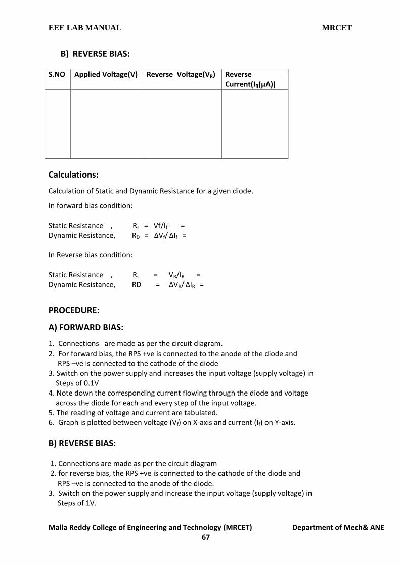
B) REVERSE BIAS:
S.NO Applied Voltage(V) Reverse Voltage(VR) Reverse Current(IR(µA))
Calculations:
Calculation of Static and Dynamic Resistance for a given diode.
In forward bias condition: Static Resistance , Rs = Vf/If = Dynamic Resistance, RD = ∆Vf/ ∆If = In Reverse bias condition: Static Resistance , Rs = VR/IR = Dynamic Resistance, RD = ∆VR/ ∆IR =
PROCEDURE:
A) FORWARD BIAS:
1. Connections are made as per the circuit diagram. 2. For forward bias, the RPS +ve is connected to the anode of the diode and RPS –ve is connected to the cathode of the diode 3. Switch on the power supply and increases the input voltage (supply voltage) in Steps of 0.1V 4. Note down the corresponding current flowing through the diode and voltage across the diode for each and every step of the input voltage. 5. The reading of voltage and current are tabulated. 6. Graph is plotted between voltage (Vf) on X-axis and current (If) on Y-axis.
B) REVERSE BIAS: 1. Connections are made as per the circuit diagram 2. for reverse bias, the RPS +ve is connected to the cathode of the diode and RPS –ve is connected to the anode of the diode. 3. Switch on the power supply and increase the input voltage (supply voltage) in Steps of 1V.

EEE LAB MANUAL MRCET
Malla Reddy College of Engineering and Technology (MRCET) Department of Mech& ANE 68
4. Note down the corresponding current flowing through the diode voltage across the diode for each and every step of the input voltage. 5. The readings of voltage and current are tabulated 6. Graph is plotted between voltage (VR) on X-axis and current (IR) on Y-axis.
PRECAUTIONS: 1. All the connections should be correct. 2. Parallax error should be avoided while taking the readings from the Analog meters.
RESULT:
EXERCISE QUESTIONS: 1. The reverse saturation current of a silicon p – n function diode at an operating temperature of 270C is 50 nA. Compute the dynamic forward and reverse resistances of the diode for applied voltages of 0.8 V and -0.4 V respectively 2. Find the value of D.C. resistance and A.C resistance of a Germanium junction diode at 250
C with reverse saturation current, Io = 25μA and at an applied voltage of 0.2V across the
diode
VIVA QUESTIONS:
1. Define depletion region of a diode? 2. What is meant by transition & space charge capacitance of a diode? 3. Is the V-I relationship of a diode Linear or Exponential? 4. Define cut-in voltage of a diode and specify the values for Si and Ge diodes? 5. What are the applications of a p-n diode? 6. Draw the ideal characteristics of P-N junction diode? 7. What is the diode equation? 8. What is PIV? 9. What is the break down voltage? 10. What is the effect of temperature on PN junction diodes?

EEE LAB MANUAL MRCET
Malla Reddy College of Engineering and Technology (MRCET) Department of Mech& ANE 69
2. ZENER DIODE CHARACTERISTICS AND ZENER AS VOLTAGE REGULATOR
AIM: a) To observe and draw the static characteristics of a zener diode
b) To find the voltage regulation of a given zener diode
APPARATUS:
1. Zener diode - 1No. 2. Regulated Power Supply (0-30v) - 1No. 3. Voltmeter (0-20v) - 1No. 4. Ammeter (0-20mA) - 1No.
5. Resistor (1K ohm) 6. Bread Board 7. Connecting wires
THEORY: A zener diode is heavily doped p-n junction diode, specially made to operate in
the break down region. A p-n junction diode normally does not conduct when reverse biased. But if the reverse bias is increased, at a particular voltage it starts conducting heavily. This voltage is called Break down Voltage. High current through the diode can permanently damage the device
To avoid high current, we connect a resistor in series with zener diode. Once
the diode starts conducting it maintains almost constant voltage across the terminals whatever may be the current through it, i.e., it has very low dynamic resistance. It is used in voltage regulators.
CIRCUIT DIAGRAM
A) STATIC CHARACTERISTICS :

EEE LAB MANUAL MRCET
Malla Reddy College of Engineering and Technology (MRCET) Department of Mech& ANE 70
b) REVERSE BIAS CHARACTERISTICS:

EEE LAB MANUAL MRCET
Malla Reddy College of Engineering and Technology (MRCET) Department of Mech& ANE 71
OBSERVATIONS: A) FORWARD BIAS characteristics:
S.NO Applied Voltage(V) Forward Voltage(Vf) Forward Current(If(mA))
B) REVERSE BIAS Characteristics:
S.NO Applied Voltage(V) Reverse Voltage(VR) Reverse Current(IR(mA))

EEE LAB MANUAL MRCET
Malla Reddy College of Engineering and Technology (MRCET) Department of Mech& ANE 72
PROCEDURE: A) Static characteristics: 1. Connections are made as per the circuit diagram. 2. The Regulated power supply voltage is increased in steps. 3. The Forward current (lf), and the forward voltage (Vf.) are observed and then noted in the tabular form. 4. A graph is plotted between Forward current (lf) on X-axis and the forward voltage (Vf) on Y-axis.
B) Regulation characteristics:
LOAD REGULATION CHARACTERISTICS: 1. Connect the Circuit as per the Circuit Diagram on the bread board. 2. By changing the load Resistance, kept constant I/P Voltage at 5V, 10 V, 15 V as Per table given below. Take the readings of O/P Voltmeter (Vo=Vz). 3. Now by changing the I/P Voltage, kept constant load Resistance at 1K, 2K, 3K as
per table given below. Take the readings of O/P Voltmeter (Vo=Vz).
LOAD REGULATION LINE REGULATION
PRECAUTIONS:
1. The terminals of the zener diode should be properly identified 2. While determined the load regulation, load should not be immediately shorted. 3. Should be ensured that the applied voltages & currents do not exceed the ratings of
the diode.
RESULT:

EEE LAB MANUAL MRCET
Malla Reddy College of Engineering and Technology (MRCET) Department of Mech& ANE 73
EXERCISE QUESTIONS:
1. A Zener voltage regulator circuit is to maintain constant voltage at 60 V, over a current range from 5 to 50 mA. The input supply voltage is 200 V. Determine the value of resistance R to be connected in the circuit, for voltage regulation from load current IL = 0
mA to IL max, the maximum possible value of IL. What is the value IL max?
VIVAQUESTIONS:
1. What type of temp coefficient does the zener diode have? 2. If the impurity concentration is increased, how the depletion width effected? 3. Does the dynamic impendence of a zener diode vary? 4. Explain briefly about avalanche and zener breakdowns? 5. Draw the zener equivalent circuit? 6. Differentiate between line regulation & load regulation? 7. In which region zener diode can be used as a regulator? 8. How the breakdown voltage of a particular diode can be controlled? 9. What type of temperature coefficient does the Avalanche breakdown has? 10. By what type of charge carriers the current flows in zener and avalanche breakdown
diodes?

EEE LAB MANUAL MRCET
Malla Reddy College of Engineering and Technology (MRCET) Department of Mech& ANE 74
3. HALF -WAVE RECTIFIER WITH AND WITHOUT FILTER
AIM: To examine the input and output waveforms of half wave Rectifier and also
calculate its load regulation and ripple factor. 1. with Filter 2. without Filter
APPARATUS:
Digital multimetersMultimeter - 1No. Transformer (6V-0-6V) - 1No. Diode, 1N4007 - 1No. Capacitor 100μf/470 μf - 1No. Decade Resistance Box - 1No. Breadboard CRO and CRO probes Connecting wires
THEORY: In Half Wave Rectification, When AC supply is applied at the input, only Positive Half Cycle appears across the load whereas, the negative Half Cycle is suppressed. How this can be explained as follows: During positive half-cycle of the input voltage, the diode D1 is in forward bias and conducts through the load resistor RL. Hence the current produces an output voltage across the load resistor RL, which has the same shape as the +ve half cycle of the input voltage.
During the negative half-cycle of the input voltage, the diode is reverse biased and there is no current through the circuit. i.e., the voltage across RL is zero. The net result is that only the +ve half cycle of the input voltage appears across the load. The average value of the half wave rectified o/p voltage is the value measured on dc voltmeter. For practical circuits, transformer coupling is usually provided for two reasons.
1. The voltage can be stepped-up or stepped-down, as needed. 2. The ac source is electrically isolated from the rectifier. Thus preventing shock
hazards in the secondary circuit. The efficiency of the Half Wave Rectifier is 40.6%

EEE LAB MANUAL MRCET
Malla Reddy College of Engineering and Technology (MRCET) Department of Mech& ANE 75
Theoretical calculations for Ripple factor:
Without Filter:
Vrms=Vm/2
Vm=2Vrms
Vdc=Vm/П
Ripple factor r=√ (Vrms/ Vdc )2 -1 =1.21
With Filter:
Ripple factor, r=1/ (2√3 f C R)
CIRCUIT DIAGRAM: A) Half wave Rectifier without filter:
B) Half wave Rectifier with filter

EEE LAB MANUAL MRCET
Malla Reddy College of Engineering and Technology (MRCET) Department of Mech& ANE 76
MODEL WAVEFORMS:
PROCEDURE: 1. Connections are made as per the circuit diagram. 2. Connect the primary side of the transformer to ac mains and the secondary side to the rectifier input.
3.By the multimeter, measure the ac input voltage of the rectifier and, ac and dc voltage at the output of the rectifier. 4. Find the theoretical of dc voltage by using the formula,
Vdc=Vm/П Where, Vm=2Vrms, (Vrms=output ac voltage.) 5. The Ripple factor is calculated by using the formula
r = ac output voltage/dc output voltage.
WITHOUT FILTER:

EEE LAB MANUAL MRCET
Malla Reddy College of Engineering and Technology (MRCET) Department of Mech& ANE 77
WITH CAPACITOR FILTER:
REGULATION CHARACTERSTICS: 1. Connections are made as per the circuit diagram. 2. By increasing the value of the rheostat, the voltage across the load and current
flowing through the load are measured. 3. The reading is tabulated. 4. From the value of no-load voltages, the %regulation is calculated using the
formula, %Regulation = [(VNL-VFL) /VFL]*100
PRECAUTIONS:
1. The primary and secondary side of the transformer should be carefully identified 2. The polarities of all the diodes should be carefully identified. 3. While determining the % regulation, first Full load should be applied and then it should be decremented in steps.
RESULT: EXERCISE QUESTIONS: 1. A half wave rectifier having a resistor load of 1000 ohms rectifier an alternating of 325V peak value and the diode has a forward resistance of 100 ohms calculate a) peak ,average and RMS value of current) dc power output c ) A.C input power and d) efficiency of the rectifier

EEE LAB MANUAL MRCET
Malla Reddy College of Engineering and Technology (MRCET) Department of Mech& ANE 78
VIVA QUESTIONS:
1. What is the PIV of Half wave rectifier? 2. What is the efficiency of half wave rectifier? 3. What is the rectifier? 4. What is the difference between the half wave rectifier and full wave Rectifier? 5. What is the o/p frequency of Bridge Rectifier? 6. What are the ripples? 7. What is the function of the filters? 8. What is TUF? 9. What is the average value of o/p voltage for HWR? 10. What is the peak factor?

EEE LAB MANUAL MRCET
Malla Reddy College of Engineering and Technology (MRCET) Department of Mech& ANE 79
4. FULL-WAVE RECTIFIER WITH AND WITHOUT FILTER
AIM: To Examine the input and output waveforms of Full Wave Rectifier and also
calculate its load regulation and ripple factor. 1. with Filter 2. without Filter
APPARATUS:
Digital multimetersMultimeter - 1No.
Transformer (6V-0-6V) - 1No. Diode, 1N4007 - 2No. Capacitor 100μf/470 μf - 1No. Decade Resistance Box - 1No. Breadboard CRO and CRO probes Connecting wires
THEORY:
The circuit of a center-tapped full wave rectifier uses two diodes D1&D2. During positive half cycle of secondary voltage (input voltage), the diode D1 is forward biased and D2is reverse biased. So the diode D1 conducts and current flows through load resistor RL.
During negative half cycle, diode D2 becomes forward biased and D1 reverse
biased. Now, D2 conducts and current flows through the load resistor RL in the same direction. There is a continuous current flow through the load resistor RL, during both the half cycles and will get unidirectional current as show in the model graph. The difference between full wave and half wave rectification is that a full wave rectifier allows unidirectional (one way) current to the load during the entire 360 degrees of the input signal and half-wave rectifier allows this only during one half cycle (180 degree).
THEORITICAL CALCULATIONS: Vrms = Vm/ √2 Vm =Vrms√2 Vdc=2Vm/П
(i)Without filter: Ripple factor, r = √ (Vrms/ Vdc )2 -1 = 0.812
(ii)With filter: Ripple factor, r = 1/ (4√3 f C RL)

EEE LAB MANUAL MRCET
Malla Reddy College of Engineering and Technology (MRCET) Department of Mech& ANE 80
CIRCUIT DIAGRAM: A) FULL WAVE RECTIFIER WITHOUT FILTER:
B) FULL WAVE RECTIFIER WITH FILTER:

EEE LAB MANUAL MRCET
Malla Reddy College of Engineering and Technology (MRCET) Department of Mech& ANE 81
MODEL WAVEFORMS: A) WAVEFORMS:
WITHOUT FILTER:

EEE LAB MANUAL MRCET
Malla Reddy College of Engineering and Technology (MRCET) Department of Mech& ANE 82
WITH CAPACITOR FILTER:
PROCEDURE: 1. Connections are made as per the circuit diagram. 2. Connect the ac mains to the primary side of the transformer and the secondary
side to the rectifier. 3. Measure the ac voltage at the input side of the rectifier. 4. Measure both ac and dc voltages at the output side the rectifier. 5. Find the theoretical value of the dc voltage by using the formula Vdc=2Vm/П 6. Connect the filter capacitor across the load resistor and measure the values of Vac
and Vdc at the output. 7. The theoretical values of Ripple factors with and without capacitor are calculated. 8. From the values of Vac and Vdc practical values of Ripple factors are calculated.
The practical values are compared with theoretical values.
PRECAUTIONS:
1. The primary and secondary side of the transformer should be carefully identified. 2. The polarities of all the diodes should be carefully identified.
RESULT:

EEE LAB MANUAL MRCET
Malla Reddy College of Engineering and Technology (MRCET) Department of Mech& ANE 83
EXERCISE QUESTIONS: 1. A Full wave single phase rectifier makes use of 2 diodes, the internal forward resistance of each is considered to be constant and equal to 30Ω. The load resistance is 1KΩ. The transformer secondary voltage is 200-0-200V (rms).Calculate VDC, IDC, and Ripple factor efficiency.
VIVA QUESTIONS:
1. Define regulation of the full wave rectifier? 2. Define peak inverse voltage (PIV)? And write its value for Full-wave rectifier? 3. If one of the diode is changed in its polarities what wave form would you get? 4. Does the process of rectification alter the frequency of the waveform? 5. What is ripple factor of the Full-wave rectifier? 6. What is the necessity of the transformer in the rectifier circuit? 7. What are the applications of a rectifier? 8. What is meant by ripple and define Ripple factor? 9. Explain how capacitor helps to improve the ripple factor? 10. Can a rectifier made in INDIA (V=230v, f=50Hz) be used in USA (V=110v, f=60Hz)?
EEE LAB MANUAL MRCET
Malla Reddy College of Engineering and Technology (MRCET) Department of Mech& ANE 84
5. INPUT AND OUTPUT CHARACTERISTICS OF TRANSISTOR CB CONFIGURATION
AIM: 1.To observe and draw the input and output characteristics of a transistor
connected in common base configuration. 2. To find α of the given transistor and also its input and output Resistances.
APPARATUS: Transistor, BC107 -1No.
Regulated power supply (0-30V) -1No. Voltmeter (0-20V) - 2No. Ammeters (0-10mA) -2No. Resistor, 1KΩ -2No Bread board Connecting wires
THEORY: A transistor is a three terminal active device. The terminals are emitter, base,
collector. In CB configuration, the base is common to both input (emitter) and output (collector). For normal operation, the E-B junction is forward biased and C-B junction is reverse biased. In CB configuration, IE is +ve, IC is –ve and IB is –ve. So,
VEB = F1 (VCB, IE) and
IC = F2 (VEB,IB)
With an increasing the reverse collector voltage, the space-charge width at the output junction increases and the effective base width ‘W’ decreases. This phenomenon is known as “Early effect”. Then, there will be less chance for recombination within the base region. With increase of charge gradient with in the base region, the current of minority carriers injected across the emitter junction increases. The current amplification factor of CB configuration is given by,
α = ∆IC/ ∆IE
Input Resistance, ri = ∆VBE /∆IE at Constant VCB
Output Résistance, ro = ∆VCB /∆IC at Constant IE

EEE LAB MANUAL MRCET
Malla Reddy College of Engineering and Technology (MRCET) Department of Mech& ANE 85
CIRCUIT:
MODEL GRAPHS:
A) INPUT CHARACTERISTICS
B) OUTPUTCHARACTERISTICS

EEE LAB MANUAL MRCET
Malla Reddy College of Engineering and Technology (MRCET) Department of Mech& ANE 86
OBSERVATIONS: A) INPUT CHARACTERISTICS:
VEE(V) VCB=1V VCB= = 2V VCB= 4V
VEB(V) IE(mA) VEB(V) IE(mA) VEB(V) IE(mA)
B) OUTPUT CHARACTERISTICS:
Vcc(V) IE=10mA IE=20mA IE=30mA
VCB(V) IC(mA) VCB(V) IC(mA) VCB(V) IC(mA)
PROCEDURE:
A) INPUT CHARACTERISTICS:
1. Connections are made as per the circuit diagram. 2. For plotting the input characteristics, the output voltage VCE is kept constant at 0V and for different values of VEE ,note down the values of IE and VBE 3. Repeat the above step keeping VCB at 2V, 4V, and 6V and all the readings are tabulated. 4. A graph is drawn between VEB and IE for constant VCB.
B) OUTPUT CHARACTERISTICS:
1. Connections are made as per the circuit diagram. 2. For plotting the output characteristics, the input IE is kept constant at 0.5mA and for
different values of VCC, note down the values of IC and VCB. 3. Repeat the above step for the values of IE at 1mA, 5mA and all the readings are
tabulated. 4. A graph is drawn between VCB and Ic for constant IE

EEE LAB MANUAL MRCET
Malla Reddy College of Engineering and Technology (MRCET) Department of Mech& ANE 87
PRECAUTIONS:
1. The supply voltages should not exceed the rating of the transistor. 2. Meters should be connected properly according to their polarities.
RESULT: EXERCISE QUESTIONS: 1. Calculate the collector current and emitter current for a transistor with αD.C. = 0.99 and
ICBO = 20 µA when the base current is 50µ A.
VIVA QUESTIONS:
1. What is the range of α for the transistor? 2. Draw the input and output characteristics of the transistor in CB configuration? 3. Identify various regions in output characteristics? 4. What is the relation between α and β? 5. What are the applications of CB configuration? 6. What are the input and output impedances of CB configuration? 7. Define α (alpha)? 8. What is early effect? 9. Draw Circuit diagram of CB configuration for PNP transistor? 10. What is the power gain of CB configuration?

EEE LAB MANUAL MRCET
Malla Reddy College of Engineering and Technology (MRCET) Department of Mech& ANE 88
6. INPUT AND OUTPUT CHARACTERISTICS OF TRASISTOR CE CONFIGURATION
AIM:
1. To draw the input and output characteristics of transistor connected in CE configuration 2. To find β of the given transistor and also its input and output Resistances
APPARATUS: Transistor, BC107 -1No.
Regulated power supply (0-30V) -1No. Voltmeter (0-20V) -2No. Ammeters (0-20mA) -1No. Ammeters (0-200μA) -1No. Resistor, 100Ω -1No Resistor, 1KΩ -1No. Bread board Connecting wires
THEORY: In common emitter configuration, input voltage is applied between base and emitter terminals and out put is taken across the collector and emitter terminals. Therefore the emitter terminal is common to both input and output. The input characteristics resemble that of a forward biased diode curve. This is expected since the Base-Emitter junction of the transistor is forward biased. As compared to CB arrangement IB increases less rapidly with VBE. Therefore input resistance of CE circuit is higher than that of CB circuit. The output characteristics are drawn between Ic and VCE at constant IB. the collector current varies with VCE upto few volts only. After this the collector current becomes almost constant, and independent of VCE. The value of VCE up to which the collector current changes with V CE is known as Knee voltage. The transistor always operated in the region above Knee voltage, IC is always constant and is approximately equal to IB.The current amplification factor of CE configuration is given by β = ΔIC/ΔIB
Input Resistance, ri = ∆VBE /∆IB (μA) at Constant VCE
Output Résistance, ro = ∆VCE /∆IC at Constant IB (μA)

EEE LAB MANUAL MRCET
Malla Reddy College of Engineering and Technology (MRCET) Department of Mech& ANE 89
CIRCUIT DIAGRAM:
MODEL GRAPHS: A) INPUT CHARACTERISTICS:
B) OUTPUT CHARACTERSITICS:

EEE LAB MANUAL MRCET
Malla Reddy College of Engineering and Technology (MRCET) Department of Mech& ANE 90
OBSERVATIONS:
A) INPUT CHARACTERISTICS:
VBB
VCE = 1V VCE = 2V VCE = 4V
VBE(V) IB(μA) VBE(V) IB(μA) VBE(V) IB(μA)
B) OUTPUT CHAREACTARISTICS:
S.NO IB = 50 μA IB = 75 μA IB = 100 μA
VCE(V) IC(mA) VCE(V) IC(mA) VCE(V) IC(mA)
PROCEDURE:
INPUT CHARECTERSTICS:
1. Connect the circuit as per the circuit diagram. 2. For plotting the input characteristics the output voltage VCE is kept constant at 1V
and for different values of VBB , note down the values of IB and VBE 3. Repeat the above step by keeping VCE at 2V and 4V and tabulate all the readings. 4. plot the graph between VBE and IB for constant VCE
OUTPUT CHARACTERSTICS:
1. Connect the circuit as per the circuit diagram 2. For plotting the output characteristics the input current IB is kept constant at 50μA
and for different values of VCC note down the values of IC and VCE

EEE LAB MANUAL MRCET
Malla Reddy College of Engineering and Technology (MRCET) Department of Mech& ANE 91
3. Repeat the above step by keeping IB at 75 μA and 100 μA and tabulate the all the readings
4. Plot the graph between VCE and IC for constant IB
PRECAUTIONS:
1. The supply voltage should not exceed the rating of the transistor 2. Meters should be connected properly according to their polarities
RESULT: EXERCISE QUESTIONS:
1. For an NPN transistor with αN= 0.98, ICO= 2μA and IEO= 1.6μA connected in Common Emitter Configuration, calculate the minimum base current for which the transistor enters into saturation region. VCC and load resistance are given as 12 V and 4.0 KΩ respectively.
2. Calculate the values of IE, αdc and βdc for a transistor with IB=13µA, IC=200mA, ICBO=6µA. Also determine the new level of IC which will result from reducing IB to 100 mA.
VIVA QUESTIONS:
1. What is the range of β for the transistor? 2. What are the input and output impedances of CE configuration? 3. Identify various regions in the output characteristics? 4. What is the relation between α and β? 5. Define current gain in CE configuration? 6. Why CE configuration is preferred for amplification? 7. What is the phase relation between input and output? 8. Draw diagram of CE configuration for PNP transistor? 9. What is the power gain of CE configuration? 10. What are the applications of CE configuration?