elct 501: digital system design - german …eee.guc.edu.eg/courses/electronics/elct501 digital...
TRANSCRIPT

ELCT 501:
Digital System Design
Lecture 8: System Design
Dr. Mohamed Abd El Ghany,
Department of Electronics and Electrical Engineering

Algorithmic State Machine (ASM)
2Dr. Mohamed Abd el Ghany
Department of Electronics and Electrical Engineering
ELCT 501: Digital System
Design
For large machines, the designers often use
a different form of representation, called the
algorithmic state machine chart.
An ASM chart is a type of flowchart that can
be used to represent the state transitions
and generated outputs for an FSM.

Elements used in ASM Charts
3Dr. Mohamed Abd el Ghany
Department of Electronics and Electrical Engineering
ELCT 501: Digital System
Design
Output
signals or
actions
(Moore type)
Condition
expression
Conditional outputs or
actions (Mealy type)
State name
0 (false) 1 (true)
State box Decision box
Conditional output box

From FSM to ASM chart
4Dr. Mohamed Abd el Ghany
Department of Electronics and Electrical Engineering
ELCT 501: Digital System
Design
A
Reset
w0
1B
w0
1
Z
C
w0 1

From FSM to ASM chart
5Dr. Mohamed Abd el Ghany
Department of Electronics and Electrical Engineering
ELCT 501: Digital System
Design
A
Reset
w0
1B
w0 1
z

Design Example
6Dr. Mohamed Abd el Ghany
Department of Electronics and Electrical Engineering
ELCT 501: Digital System
Design
Design A Bit-Counting Circuit to count the
number of bits in a register
B = 0;
While A ≠ 0 do
if a0 = 1 then
B= B+1;
end if;
Right-shift A;
End while;
Pseudo-
code for
the bit
counter

ASM chart for the
pseudo-code
7Dr. Mohamed Abd el Ghany
Department of Electronics and Electrical Engineering
ELCT 501: Digital System
Design
B = 0;
While A ≠ 0 do
if a0 = 1 then
B= B+1;
end if;
Right-shift A;
End while;
B <- 0
S1
Reset
s0
1
S2
A=0?
0
1
Shift right A
Load A
a00
B<-B+1
Done
s
1
1
0
S3

Datapath for the ASM chart
8Dr. Mohamed Abd el Ghany
Department of Electronics and Electrical Engineering
ELCT 501: Digital System
Design
Shift register
Data
Counter
Clock
L
E
w
L
E
0
log2nn
log2n
LB
EB
0
LA
EA
A
n
B
a0z

ASM chart for the
control circuit
9Dr. Mohamed Abd el Ghany
Department of Electronics and Electrical Engineering
ELCT 501: Digital System
Design
LB
S1
Reset
s0
1
S2
z
0
1
EA
a00
EB
Done
s
1
1
0
S3

VHDL for the bit-
counting circuit
10Dr. Mohamed Abd el Ghany
Department of Electronics and Electrical Engineering
ELCT 501: Digital System
Design
Part 1

VHDL for the bit-
counting circuit
11Dr. Mohamed Abd el Ghany
Department of Electronics and Electrical Engineering
ELCT 501: Digital System
Design
Part 2

VHDL for the bit-
counting circuit
12Dr. Mohamed Abd el Ghany
Department of Electronics and Electrical Engineering
ELCT 501: Digital System
Design
Part 3

VHDL for the bit-
counting circuit
13Dr. Mohamed Abd el Ghany
Department of Electronics and Electrical Engineering
ELCT 501: Digital System
Design
Part 4

Design Example
14Dr. Mohamed Abd el Ghany
Department of Electronics and Electrical Engineering
ELCT 501: Digital System
Design
Design a shift-and-add multiplier
Decimal
13
x 11
-----------
13
13
-----------
143Manual
method
Binary
1101
x 1011
--------------
1101
1101
0000
1101
---------------
10001111

Design Example
15Dr. Mohamed Abd el Ghany
Department of Electronics and Electrical Engineering
ELCT 501: Digital System
Design
Design a shift-and-add multiplier
P = 0;
For i =0 to n-1 do
if bi = 1 then
P= P+A;
end if;
Left-shift A;
End For;
Pseudo-
code
Binary
1101
x 1011
--------------
1101
1101
0000
1101
---------------
10001111

ASM chart for the
multiplier
16Dr. Mohamed Abd el Ghany
Department of Electronics and Electrical Engineering
ELCT 501: Digital System
Design
P <- 0
S1
Reset
s0
1
S2
B=0?
0
1
Shift left A,
Shift right B
Load A
Load B
b00
P<-P+A
Done
s
1
1
0
S3
Binary
1101
x 1011
--------------
1101
1101
0000
1101
---------------
10001111
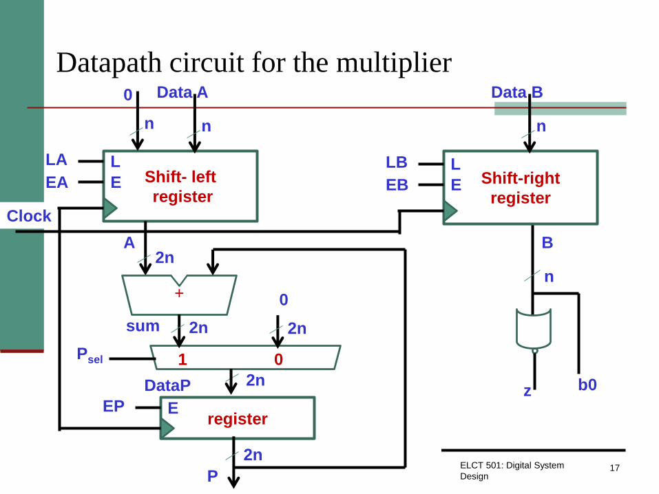
Datapath circuit for the multiplier
17Dr. Mohamed Abd el Ghany
Department of Electronics and Electrical Engineering
ELCT 501: Digital System
Design
Shift- left
register
Data A
Clock
L
E
n
LA
EA
B
n
b0z
Shift-right
register
Data B
L
E
n
LB
EB
n
0
+
2nA
sum 2n 2n
0
1 0Psel
registerEEP
2n
P
2nDataP

ASM chart for the
multiplier control circuit
18Dr. Mohamed Abd el Ghany
Department of Electronics and Electrical Engineering
ELCT 501: Digital System
Design
Psel=0, EP
S1
Reset
s0
1
S2
z
0
1
Psel=1,
EA, EB
b00
EP
Done
s
1
1
0
S3
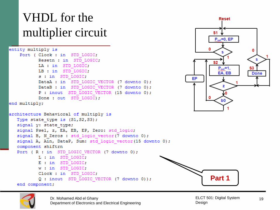
VHDL for the
multiplier circuit
19Dr. Mohamed Abd el Ghany
Department of Electronics and Electrical Engineering
ELCT 501: Digital System
Design
Part 1

VHDL for the
multiplier circuit
20Dr. Mohamed Abd el Ghany
Department of Electronics and Electrical Engineering
ELCT 501: Digital System
Design
Part 2

VHDL for the
multiplier circuit
21Dr. Mohamed Abd el Ghany
Department of Electronics and Electrical Engineering
ELCT 501: Digital System
Design
Part 3

VHDL for the
multiplier circuit
22Dr. Mohamed Abd el Ghany
Department of Electronics and Electrical Engineering
ELCT 501: Digital System
Design
Part 4

Clock Synchronization
23Dr. Mohamed Abd el Ghany
Department of Electronics and Electrical Engineering
ELCT 501: Digital System
Design
Clock
enable
circuit
clock
Dat
a D Q
Q’E
Clock Skew: If the circuit of clock enable is used,
then the flip-flops without the enable
input will observe changes in the
clock signal slightly earlier than the
flip-flops that have the enable input.
This situation , in which the clock
signal arrives at different times at
different flip-flops, is known as clock
skew.
Similar problems arise in a chip in
which the clock signal is distributed
to different flip-flops by wires whose
lengths vary appreciably.

Clock Synchronization
24Dr. Mohamed Abd el Ghany
Department of Electronics and Electrical Engineering
ELCT 501: Digital System
Design
Clock Skew: For proper operation of
synchronous sequential
circuits, it is essential to
minimize the clock skew as
much as possible.
The clock signal is
distributed to the flip-flops
such that the length of wire
between each flip-flop and
clock source is the same.
An H tree clock
distribution network