efficiency vs. output current enpirion power datasheet v v ... · enpirion® power datasheet ......
TRANSCRIPT

Enpirion® Power Datasheet
EN2342QI 4A PowerSoC
Voltage Mode Synchronous PWM Buck with Integrated Inductor
www.altera.com/enpirion
Description
The EN2342QI is a Power System on a Chip (PowerSoC) DC-DC converter. It integrates MOSFET switches, small-signal control circuits, compensation and an integrated inductor in an advanced 8x11x3mm QFN module. It offers high efficiency, excellent line and load regulation over temperature and up to the full 4A load range. The EN2342QI operates over a wide input voltage range and is specifically designed to meet the precise voltage and fast transient requirements of high-performance products. The EN2342 features frequency synchronization to an external clock, power OK output voltage monitor, programmable soft-start along with thermal and over current protection. The device’s advanced circuit design, ultra high switching frequency and proprietary integrated inductor technology delivers high-quality, ultra compact, non-isolated DC-DC conversion.
The Altera Enpirion solution significantly helps in system design and productivity by offering greatly simplified board design, layout and manufacturing requirements. In addition, overall system level reliability is improved given the small number of components required with the Altera Enpirion solution.
All Altera Enpirion products are RoHS compliant, halogen free and are compatible with lead-free manufacturing environments.
Features
Integrated Inductor, MOSFETs, Controller
Wide Input Voltage Range: 4.5V – 14V
Guaranteed 4A IOUT at 85°C with No Airflow
Frequency Synchronization (External Clock)
1.5% VOUT Accuracy (Over Load and Temperature)
High Efficiency (Up to 95%)
Output Enable Pin and Power OK signal
Programmable Soft-Start Time
Pre-Bias Protection
Pin Compatible with the EN2340/60QI
Under Voltage Lockout Protection (UVLO)
Thermal Soft-Shutdown Protection
Over Current and Short Circuit Protection
RoHS Compliant, MSL Level 3, 260oC Reflow
Applications
FPGA Applications, Core, IO, Transceiver
Space Constrained Applications
Output Voltage Ripple Sensitive Applications
Beat Frequency Sensitive Applications
Servers, Embedded Computing Systems, LAN/SAN Adapter Cards, RAID Storage Systems, Industrial Automation, Test and Measurement, and Telecommunications
Figure 1. Simplified Application Circuit Figure 2. Highest Efficiency in Smallest Solution Size
VOUTVIN
22F
1206
VOUT
ENABLE
AGND
PVIN
AVIN
PGND PGND
47nF
VFB
RA
RB
RCA
CA
RCLX
COUT
AVINO
PG BTMP
EN2342QI
SS
VDDB BGND
FQADJ
RVB
4.75k
1F
0.22F22nF
RFS RCLX
1F
OFF
ON
EN_PB
50
55
60
65
70
75
80
85
90
95
0 0.5 1 1.5 2 2.5 3 3.5 4
EF
FIC
IEN
CY
(%
)
OUTPUT CURRENT (A)
Efficiency vs. Output Current
VOUT = 5.0V
VOUT = 1.8V
CONDITIONSVIN = 12.0V
Dual Supply
Actual Solution Size200mm2
09520 September 14, 2015 Rev F

EN2342QI
www.altera.com/enpirion, Page 2
Ordering Information
Part Number Package Markings TAMBIENT Rating (°C) Package Description
EN2342QI EN2342QI -40 to +85 68-pin (8mm x 11mm x 3mm) QFN T&R
EVB-EN2342QI EN2342QI QFN Evaluation Board
Packing and Marking Information: www.altera.com/support/reliability/packing/rel-packing-and-marking.html
Pin Assignments (Top View)
Figure 3: Pin Out Diagram (Top View)
NOTE A: NC pins are not to be electrically connected to each other or to any external signal, ground, or voltage. All pins including NC pins must be soldered to the PCB. Failure to follow this guideline may result in part malfunction or damage.
NOTE B: Shaded area highlights exposed metal below the package that is not to be mechanically or electrically connected to the PCB. Refer to Figure 12 for details.
NOTE C: White ‘dot’ on top left is pin 1 indicator on top of the device package.
NC 1
NC
NC
NC
NC
NC
NC
NC
NC
NC
NC
NC
NC
NC
2
3
4
5
6
7
8
9
VO
UT
VO
UT
NC
VO
UT
VO
UT
VO
UT
VO
UT
VO
UT
VO
UT
VO
UT
NC
NC
NC
(SW
)
NC
(SW
)
PG
ND
PG
ND
PG
ND
PG
ND
PG
ND
PG
ND
PVIN
PVIN
PVIN
PVIN
PVIN
PVIN
PVIN
AVINO
PG
BGND
VDDB
S_IN
BTMP
S_OUT
NC
NC
NC
NC
NC
NC
(SW
)
NC
(SW
)
FQ
AD
J
NC
RC
LX
SS
EA
OU
T
VF
B
AG
ND
AG
ND
AV
IN
EN
AB
LE
PO
K
10
11
12
13
14
15
16
17
18
19
20
21
22
23
24
25
26
27
28
29
30
31
32
33
34
48
47
46
45
44
43
42
41
40
39
38
37
36
35
68
67
66
65
64
63
62
61
60
59
58
57
56
55
54 53
52 51
50
49
69
PGND
KEEP OUT
KEEP OUT
KE
EP
OU
T
EN
_P
B
NC
(SW
)
09520 September 14, 2015 Rev F

EN2342QI Datasheet
www.altera.com/enpirion
Pin Description
I/O Legend: P=Power G=Ground NC=No Connect I=Input O=Output I/O=Input/Output
PIN NAME I/O FUNCTION 1-15, 25-26, 59, 64-
68
NC NC NO CONNECT – These pins may be internally connected. Do not connect them to each other or to any other electrical signal. Failure to follow this guideline may result in device damage.
16-24 VOUT O Regulated converter output. Connect these pins to the load and place output capacitor between these pins and PGND pins 29-34.
27-28, 61-63
NC(SW) NC NO CONNECT – These pins are internally connected to the common switching node of the internal MOSFETs. They are not to be electrically connected to any external signal, ground, or voltage. Failure to follow this guideline may result in damage to the device.
29-34 PGND G Input/output power ground. Connect these pins to the ground electrode of the input and output filter capacitors. See VOUT and PVIN pin descriptions for more details.
35-41 PVIN P Input power supply. Connect to input power supply. Decouple with input capacitor to PGND pins 29-34.
42 AVINO O
Internal 3.3V linear regulator output. Connect this pin to AVIN (Pin 51) for applications where operation from a single input voltage (PVIN) is required. If AVINO is being used, place a 1µF, X5R/X7R, capacitor between AVINO and AGND as close as possible to AVINO.
43 PG I/O PMOS gate. Place a 22nF, X5R/X7R, capacitor between this pin and BTMP. A 560Ω may be used between PVIN and PG to assist in filtering the input rail in noisy systems.
44 BTMP I/O Bottom plate ground. See pin 43 description.
45 VDDB O Internal regulated voltage used for the internal control circuitry. Place a 0.22µF, X5R/X7R, capacitor between this pin and BGND.
46 BGND G Ground for VDDB. See pin 45 description.
47 S_IN I Digital synchronization input. This pin accepts either an input clock to phase lock the internal switching frequency or a S_OUT signal from another EN2342QI. Leave this pin floating if not used.
48 S_OUT O Digital synchronization output. PWM signal is output on this pin. Leave this pin floating if not used.
49 POK O Power OK is an open drain transistor (pulled up to AVIN or similar voltage) used for power system state indication. POK is logic high when VOUT is within -10% of VOUT nominal. Leave this pin floating if not used.
50 ENABLE I Output enable. Applying a logic high to this pin enables the output and initiates a soft-start. Applying a logic low disables the output. ENABLE logic cannot be higher than AVIN (refer to Absolute Maximum Ratings). Do not leave floating.
51 AVIN P 3.3V Input power supply for the controller. Place a 1µF, X5R/X7R, capacitor between AVIN and AGND.
52, 53 AGND G Analog ground. This is the ground return for the controller. All AGND pins need to be connected to a quiet ground.
54 VFB I/O External feedback input. The feedback loop is closed through this pin. A voltage divider at VOUT is used to set the output voltage. The mid-point of the divider is connected to VFB. A phase lead network from this pin to VOUT is also required to stabilize the loop.
55 EAOUT O Optional error amplifier output. Allows for customization of the control loop.
56 SS I/O Soft-start node. The soft-start capacitor is connected between this pin and AGND. The value of this capacitor determines the startup time.
57 RCLX I/O
Over-current protection. Placement of a resistor on this pin will adjust the over-current protection threshold. See Table 2 for the recommended RCLX Value to set OCP at the nominal value specified in the Electrical Characteristics table. No current limit protection when this pin is left floating.
58 FQADJ I/O Adding a resistor (RFS) to this pin will adjust the switching frequency of the EN2342QI. See Table 1 for suggested resistor values on RFS for various PVIN/VOUT combinations to maximize efficiency. Do not leave floating.
60 EN_PB I Enable pre-bias protection. Connect EN_PB directly to AVIN to enable the Pre-Bias Protection feature. Pull EN_PB directly to ground to disable the feature. Do not leave this pin floating. See Pre-Bias Operation for details.
09520 September 14, 2015 Rev F

EN2342QI
www.altera.com/enpirion, Page 4
PIN NAME I/O FUNCTION
69 PGND G Not a perimeter pin. Device thermal pad to be connected to the system GND plane for heat-sinking purposes.
Absolute Maximum Ratings
CAUTION: Absolute Maximum ratings are stress ratings only. Functional operation beyond the recommended operating conditions is not implied. Stress beyond the absolute maximum ratings may impair device life. Exposure to absolute maximum rated conditions for extended periods may affect device reliability.
PARAMETER SYMBOL MIN MAX UNITS
Voltages on : PVIN, VOUT, PG -0.5 15 V
Voltages on: ENABLE, POK, EN_PB -0.3 AVIN+0.3 V
Dual Supply PVIN Rising and Falling Slew Rate (Note 1) 25 V/ms
Single Supply PVIN Rising and Falling Slew Rate (Note 1) 10 V/ms
Pin Voltages – AVINO, AVIN, S_IN, S_OUT 3.0 6.0 V
Pin Voltages – VFB, SS, EAOUT, RCLX, FQADJ, VDDB, BTMP -0.5 2.75 V
Storage Temperature Range TSTG -65 150 °C
Maximum Operating Junction Temperature TJ-ABS Max 150 °C
Reflow Temp, 10 Sec, MSL3 JEDEC J-STD-020A 260 °C
ESD Rating (based on Human Body Model) 2000 V
ESD Rating (based on CDM) 500 V
Recommended Operating Conditions
PARAMETER SYMBOL MIN MAX UNITS
Input Voltage Range PVIN 4.5 14 V
AVIN: Controller Supply Voltage AVIN 3.0 5.5 V
Output Voltage Range (Note 2) VOUT 0.75 5 V
Output Current IOUT 4 A
Operating Ambient Temperature TA -40 +85 °C
Operating Junction Temperature TJ -40 +125 °C
Thermal Characteristics
PARAMETER SYMBOL TYP UNITS
Thermal Resistance: Junction to Ambient (0 LFM) (Note 3) JA 18 °C/W
Thermal Resistance: Junction to Case (0 LFM) JC 2 °C/W
Thermal Shutdown TSD 150 °C
Thermal Shutdown Hysteresis TSDH 35 °C
Note 1: PVIN rising and falling slew rates cannot be outside of specification. After the device is powered, the input voltage transients should be kept under 1V peak-to-peak under all conditions. A noisy input rail will affect device performance. For accurate power up sequencing, use a fast ENABLE logic (>3V/100µs) after both AVIN and PVIN is high.
Note 2: Dropout: Maximum VOUT ≤ VIN - 2.5V
Note 3: Based on 2oz. external copper layers and proper thermal design in line with EIJ/JEDEC JESD51-7 standard for high thermal conductivity boards.
Characteristics
NOTE: VIN=12V, Minimum and Maximum values are over operating ambient temperature range (-40°C ≤ TA ≤ +85°C) unless otherwise noted. Typical values are at TA = 25°C.
09520 September 14, 2015 Rev F

EN2342QI
www.altera.com/enpirion, Page 5
PARAMETER SYMBOL TEST CONDITIONS MIN TYP MAX UNITS
Operating Input Voltage PVIN 4.5 14.0 V
Controller Input Voltage AVIN 3.0 5.5 V
AVIN UVLO Rising AVINUVLOR UVLO is not asserted 2.5 2.75 3.0 V
AVIN UVLO Falling AVINOVLOF UVLO is asserted 2.1 2.35 2.6 V
AVIN UVLO Hysteresis AVINHYS 400 mV
AVIN Pin Input Current IAVIN 7 15 mA
Internal LDO Output AVINO 3.3 V
Shut-Down Supply Current IPVINS PVIN=12V, AVIN=3.3V, ENABLE=0V 2 mA
IAVINS PVIN=12V, AVIN=3.3V, ENABLE=0V 300 A
Feedback Pin Voltage VFB VIN = 12V, ILOAD = 0, TA = 25°C Only 0.7425 0.750 0.7575 V
Feedback Pin Voltage (Load and Temperature)
VFB 0A ≤ ILOAD ≤ 4A
Starting Date Code: X510 or greater 0.739 0.750 0.761 V
Feedback Pin Voltage
(Line, Load, Temperature) VFB 4.5V ≤ VIN ≤ 14V; 0A ≤ ILOAD ≤ 4A 0.735 0.750 0.765 V
Feedback Pin Input Leakage Current
IFB VFB pin input leakage current
(Note 4) -5 5 nA
VOUT Rise Time tRISE CSS = 47nF (Note 5 and Note 6) 3.2 ms
Soft-Start Capacitor Range CSS_RANGE 10 47 68 nF
Output Current Range IOUT 0 4 A
Over Current Trip Level IOCP PVIN=12V, VOUT=1.2V 4.15 6 A
Short Circuit Average Input Current
IIN_AVG_OCP Short = 10mΩ (Note 7) 100 mA
Disable Threshold VDISABLE ENABLE pin logic Low 0.0 0.95 V
ENABLE Threshold VENABLE ENABLE pin logic High 1.25 AVIN V
ENABLE Hysteresis ENHYS 200 mV
ENABLE Lockout Time TENLOCKOUT 8 ms
ENABLE Input Current IENABLE 370k internal pull-down (Note 4) 4 A
Switching Frequency FSW RFS =3kΩ 1.0 MHz
External SYNC Clock Frequency Lock Range
FPLL_LOCK Range of SYNC clock frequency
(See Table 1) 0.9 1.8 MHz
S_IN Threshold – Low VS_IN_LO S_IN clock logic low level (Note 4) 0.8 V
S_IN Threshold – High VS_IN_HI S_IN clock logic high level (Note 4) 1.8 2.5 V
S_OUT Threshold – Low VS_OUT_LO S_OUT clock logic low level (Note 4) 0.8 V
S_OUT Threshold – High VS_OUT_HI S_OUT clock logic high level (Note 4) 1.8 2.5 V
POK Lower Threshold POKLT VOUT / VOUT_NOM 90 %
POK Output low Voltage VPOKL With 4mA current sink into POK 0.4 V
POK Output Hi Voltage VPOKH PVIN range: 4.5V ≤ VIN ≤ 14V AVIN V
POK VOH Leakage Current IPOKL POK High (Note 4) 1 µA
Note 4: Parameter not production tested but is guaranteed by design.
Note 5: Rise time calculation begins when AVIN > VUVLO and ENABLE = HIGH.
Note 6: VOUT Rise Time Accuracy does not include soft-start capacitor tolerance.
Note 7: Output short circuit condition was performed with load impedance that is greater than or equal to 10mΩ.
09520 September 14, 2015 Rev F
EN2342QI
www.altera.com/enpirion, Page 6
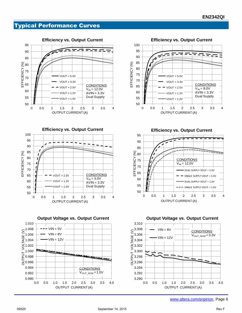
Typical Performance Curves
50
55
60
65
70
75
80
85
90
95
0 0.5 1 1.5 2 2.5 3 3.5 4
EF
FIC
IEN
CY
(%
)
OUTPUT CURRENT (A)
Efficiency vs. Output Current
VOUT = 5.0V
VOUT = 3.3V
VOUT = 2.5V
VOUT = 1.2V
VOUT = 1.0V
CONDITIONSVIN = 12.0V
AVIN = 3.3VDual Supply
50
55
60
65
70
75
80
85
90
95
100
0 0.5 1 1.5 2 2.5 3 3.5 4
EF
FIC
IEN
CY
(%
)
OUTPUT CURRENT (A)
Efficiency vs. Output Current
VOUT = 5.0V
VOUT = 3.3V
VOUT = 2.5V
VOUT = 1.2V
VOUT = 1.2V
CONDITIONSVIN = 8.0V
CONDITIONSVIN = 8.0V
AVIN = 3.3VDual Supply
50
55
60
65
70
75
80
85
90
95
100
0 0.5 1 1.5 2 2.5 3 3.5 4
EF
FIC
IEN
CY
(%
)
OUTPUT CURRENT (A)
Efficiency vs. Output Current
VOUT = 2.5V
VOUT = 1.2V
VOUT = 1.0V
CONDITIONSVIN = 8.0V
CONDITIONSVIN = 5.0V
AVIN = 3.3VDual Supply
50
55
60
65
70
75
80
85
90
95
0 0.5 1 1.5 2 2.5 3 3.5 4
EF
FIC
IEN
CY
(%
)
OUTPUT CURRENT (A)
Efficiency vs. Output Current
DUAL SUPPLY VOUT = 5.0V
SINGLE SUPPLY VOUT = 5.0V
DUAL SUPPLY VOUT = 1.0V
SINGLE SUPPLY VOUT = 1.0V
CONDITIONSVIN = 12.0V
0.990
0.992
0.994
0.996
0.998
1.000
1.002
1.004
1.006
1.008
1.010
0.0 0.5 1.0 1.5 2.0 2.5 3.0 3.5 4.0
OU
TP
UT
V
OLTA
GE
(V
)
OUTPUT CURRENT (A)
Output Voltage vs. Output Current
VIN = 5V
VIN = 8V
VIN = 12V
CONDITIONSVIN = 5.0V
CONDITIONSVOUT_NOM = 1.0V
3.290
3.292
3.294
3.296
3.298
3.300
3.302
3.304
3.306
3.308
3.310
0.0 0.5 1.0 1.5 2.0 2.5 3.0 3.5 4.0
OU
TP
UT
V
OLTA
GE
(V
)
OUTPUT CURRENT (A)
Output Voltage vs. Output Current
VIN = 8V
VIN = 12V
CONDITIONSVOUT_NOM = 3.3V
09520 September 14, 2015 Rev F
EN2342QI
www.altera.com/enpirion, Page 7
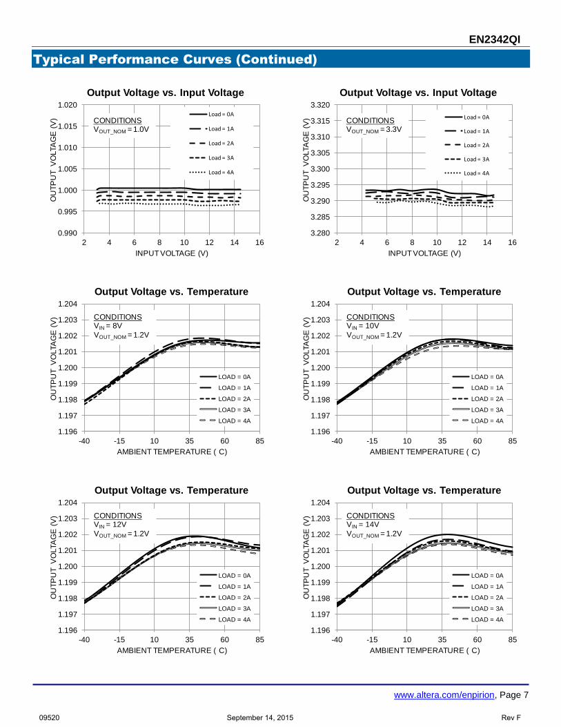
Typical Performance Curves (Continued)
0.990
0.995
1.000
1.005
1.010
1.015
1.020
2 4 6 8 10 12 14 16
OU
TP
UT
V
OLTA
GE
(V
)
INPUT VOLTAGE (V)
Output Voltage vs. Input Voltage
Load = 0A
Load = 1A
Load = 2A
Load = 3A
Load = 4A
CONDITIONSVOUT_NOM = 1.0V
3.280
3.285
3.290
3.295
3.300
3.305
3.310
3.315
3.320
2 4 6 8 10 12 14 16
OU
TP
UT
V
OLTA
GE
(V
)
INPUT VOLTAGE (V)
Output Voltage vs. Input Voltage
Load = 0A
Load = 1A
Load = 2A
Load = 3A
Load = 4A
CONDITIONSVOUT_NOM = 3.3V
1.196
1.197
1.198
1.199
1.200
1.201
1.202
1.203
1.204
-40 -15 10 35 60 85
OU
TP
UT
V
OLTA
GE
(V
)
AMBIENT TEMPERATURE ( C)
Output Voltage vs. Temperature
LOAD = 0A
LOAD = 1A
LOAD = 2A
LOAD = 3A
LOAD = 4A
CONDITIONSVIN = 8V
VOUT_NOM = 1.2V
1.196
1.197
1.198
1.199
1.200
1.201
1.202
1.203
1.204
-40 -15 10 35 60 85
OU
TP
UT
V
OLTA
GE
(V
)
AMBIENT TEMPERATURE ( C)
Output Voltage vs. Temperature
LOAD = 0A
LOAD = 1A
LOAD = 2A
LOAD = 3A
LOAD = 4A
CONDITIONSVIN = 10V
VOUT_NOM = 1.2V
1.196
1.197
1.198
1.199
1.200
1.201
1.202
1.203
1.204
-40 -15 10 35 60 85
OU
TP
UT
V
OLTA
GE
(V
)
AMBIENT TEMPERATURE ( C)
Output Voltage vs. Temperature
LOAD = 0A
LOAD = 1A
LOAD = 2A
LOAD = 3A
LOAD = 4A
CONDITIONSVIN = 12V
VOUT_NOM = 1.2V
1.196
1.197
1.198
1.199
1.200
1.201
1.202
1.203
1.204
-40 -15 10 35 60 85
OU
TP
UT
V
OLTA
GE
(V
)
AMBIENT TEMPERATURE ( C)
Output Voltage vs. Temperature
LOAD = 0A
LOAD = 1A
LOAD = 2A
LOAD = 3A
LOAD = 4A
CONDITIONSVIN = 14V
VOUT_NOM = 1.2V
09520 September 14, 2015 Rev F

EN2342QI
www.altera.com/enpirion, Page 8
Typical Performance Characteristics
VOUT
(AC Coupled)
Output Ripple at 20MHz Bandwidth
CONDITIONS
VIN = 12VVOUT = 1VIOUT = 2A
CIN = 2 x 22µF (1206)COUT = 2 x 47 µF (1206)
VOUT
(AC Coupled)
Output Ripple at 500MHz Bandwidth
CONDITIONS
VIN = 12VVOUT = 1VIOUT = 2A
CIN = 2 x 22µF (1206)COUT = 2 x 47 µF (1206)
VOUT
(AC Coupled)
Output Ripple at 20MHz Bandwidth
CONDITIONS
VIN = 12VVOUT = 1VIOUT = 4A
CIN = 2 x 22µF (1206)COUT = 2 x 47 µF (1206) VOUT
(AC Coupled)
Output Ripple at 500MHz Bandwidth
CONDITIONS
VIN = 12VVOUT = 1VIOUT = 4A
CIN = 2 x 22µF (1206)COUT = 2 x 47 µF (1206)
ENABLE
Enable Startup/Shutdown Waveform (0A)
CONDITIONS
VIN = 12V, VOUT = 1.0V, No Load, Css = 47nF
CIN = 2 x 22µF (1206), COUT = 2 x 47 µF (1206)
VOUT
POK
LOAD
ENABLE
Enable Startup/Shutdown Waveform (4A)
CONDITIONS
VIN = 12V, VOUT = 1.0V, LOAD = 4A, Css = 47nF
CIN = 2 x 22µF (1206), COUT = 2 x 47 µF (1206)
VOUT
POK
LOAD
09520 September 14, 2015 Rev F

EN2342QI
www.altera.com/enpirion, Page 9
Typical Performance Characteristics (Continued)
VOUT = 1V
(AC Coupled)
20mV / DIV
Load Transient from 50mA to 2A
CONDITIONS
VIN = 12V, VOUT = 1V
CIN = 22µF (1206)
COUT = 2 x 22µF (0805)Small Solution Size Configuration
LOAD
VOUT = 1V
(AC Coupled)
50mV / DIV
Load Transient from 50mA to 4A
CONDITIONS
VIN = 12V, VOUT = 1V
CIN = 22µF (1206)
COUT = 2 x 22µF (0805)Small Solution Size Configuration
LOAD
VOUT = 1.8V
(AC Coupled)
100mV / DIV
Load Transient from 2A to 4A
CONDITIONS
VIN = 12V, VOUT = 1.8V
CIN = 22µF (1206)
COUT = 2 x 22µF (0805)Small Solution Size Configuration
LOAD
VOUT = 1.8V
(AC Coupled)
100mV / DIV
Load Transient from 50mA to 4A
CONDITIONS
VIN = 12V, VOUT = 1.8V
CIN = 22µF (1206)
COUT = 2 x 22µF (0805)Small Solution Size Configuration
LOAD
VOUT = 3.3V
(AC Coupled)
100mV / DIV
Load Transient from 50mA to 3A
CONDITIONS
VIN = 12V, VOUT = 3.3V
CIN = 22µF (1206)
COUT = 2 x 22µF (0805)Small Solution Size Configuration
LOAD
VOUT = 3.3V
(AC Coupled)
100mV / DIV
Load Transient from 50mA to 3A
CONDITIONS
VIN = 12V, VOUT = 3.3V
CIN = 22µF (1206)
COUT = 2 x 47µF (1206)Best Performance Configuration
LOAD
09520 September 14, 2015 Rev F
EN2342QI
www.altera.com/enpirion, Page 10
Typical Performance Characteristics (Continued)
PVIN = 12V
Pre-Bias Startup Waveform
VOUT
ENABLE
CONDITIONS
VIN = 12V (Single Supply Only)
VOUT = 1.0V, Load = 0A, Css = 47nF
CIN = 22µF(1206), COUT = 2x47µF(1206)
Max Pre-Bias
<100% of Nominal
PVIN = 12V
Pre-Bias Shutdown Waveform
VOUT
ENABLE
CONDITIONS
VIN = 12V (Single Supply Only)
VOUT = 1.0V, Load = 0A, Css = 47nF
CIN = 22µF(1206), COUT = 2x47µF(1206)
VOUT is held low
for another ~6ms
09520 September 14, 2015 Rev F

EN2342QI
www.altera.com/enpirion, Page 11
Functional Block Diagram
Soft Start
Power
Good
Logic
Band Gap
Reference
Voltage Reference Generator
Compensation
Network
Thermal Limit
UVLO
Current Limit
Gate Drive
PLL/Sawtooth
GeneratorFQADJ
ENABLE
SS
AGND
POK
AVIN
VFB
PGND
VOUT
NC(SW)
PVINS_IN
Error
Amp
PWM
Comp
(+)
(-)
(-)
(+)
Digital I/O
S_OUT
To PLL
EN2342QI
Linear
Regulator AVINO
300k
370k
EAOUT
PGBTMP
BGND
VDDB
EN_PB
Figure 4: Functional Block Diagram
Functional Description
Synchronous Buck Converter
The EN2342QI is a highly integrated synchronous, buck converter with integrated controller, power MOSFET switches and inductor. The nominal input voltage (PVIN) range is 4.5V to 14V and can support up to 4A of continuous output current. The output voltage is programmed using an external resistor divider network. The control loop utilizes a Type IV Voltage-Mode compensation network and maximizes on a low-noise PWM topology. Much of the compensation circuitry is internal to the device. However, a phase lead capacitor is required along with the output voltage feedback resistor divider to complete the Type IV compensation network.. The high switching frequency of the EN2342QI enables the use of small size input and output filter
capacitors, as well as a wide loop bandwidth within a small foot print.
Protection Features:
The power supply has the following protection features:
Pre-Bias Protection
Over-Current and Short Circuit Protection
Thermal Soft-Shutdown with Hysteresis.
Under-Voltage Lockout Protection
Additional Features:
Switching Frequency Synchronization.
Programmable Soft-Start
Power OK Output Monitoring
09520 September 14, 2015 Rev F

EN2342QI
www.altera.com/enpirion, Page 12
Modes of Operation
The EN2342QI is designed to be powered by either a single input supply (PVIN) or two separate supplies: one for PVIN and the other for AVIN. The EN2342QI is not “hot pluggable.” Refer to the PVIN Slew Rate specification on page 4.
Single Input Supply Application (PVIN Only):
Figure 5: Single Input Supply Schematic
In single input supply mode, the EN2342QI only requires one input voltage rail (typically 12V). The EN2342QI has an internal linear regulator that converts PVIN to 3.3V. The output of the linear regulator is provided on the AVINO pin once the device is enabled. AVINO should be connected to AVIN. Also, in this single supply application, place a resistor (RVB) between VDDB and AVIN, as shown in Figure 5. Altera recommends RVB=4.75kΩ.
Dual Input Supply Application (PVIN and AVIN):
Figure 6: Dual Input Supply Schematic
In dual input supply mode, two input voltage rails are required (typically 12V for PVIN and 3.3V for AVIN). Refer to Figure 6 for the recommended schematic for a dual input supply application. Since AVINO is not used, it can be left open.
Enable Operation
The ENABLE pin provides a means to enable normal operation or to shut down the device. A logic high will enable the converter into normal operation. When the ENABLE pin is asserted (high) the device will undergo a normal soft-start. A logic low will disable the converter. A logic low will power down the device in a controlled manner and the device is subsequently shut down. The ENABLE signal has to be low for at least the ENABLE Lockout Time (8ms) in order for the device to be re-enabled. To ensure accurate startup sequencing the ENABLE/DISABLE signal should be faster than 1V/100µs. A slower ENABLE/DISABLE signal may result in a delayed startup and shutdown response. Do not leave ENABLE floating.
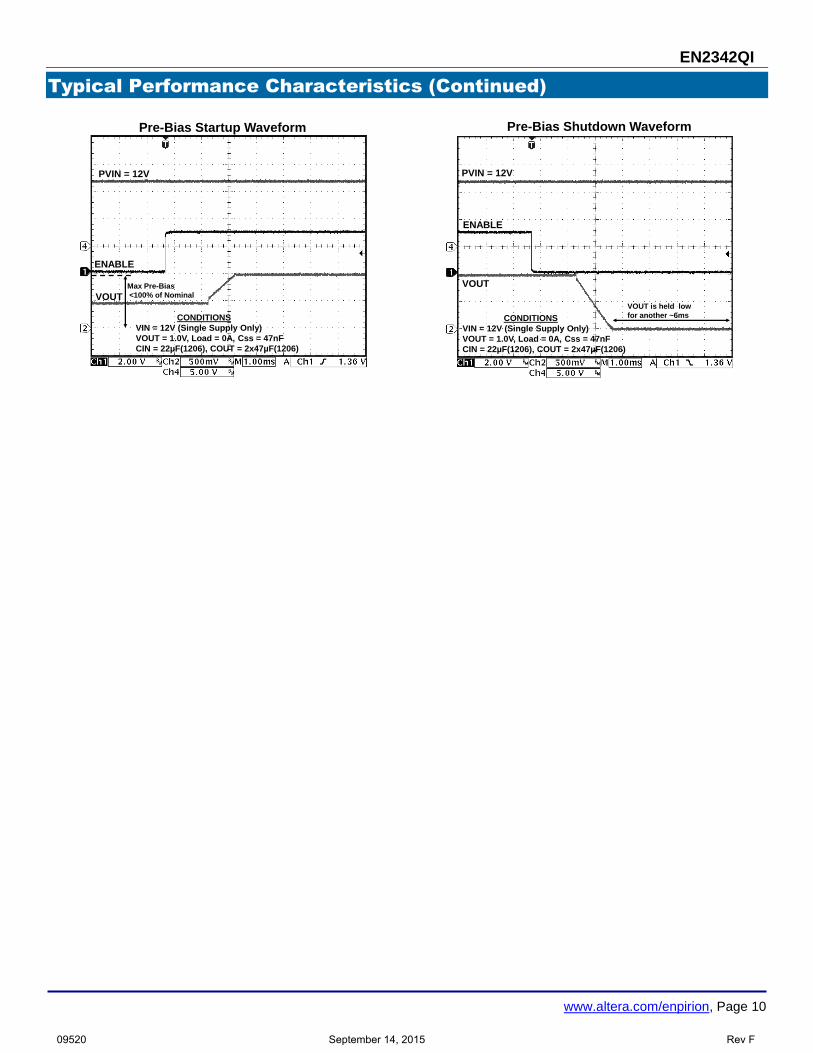
Pre-Bias Operation
The EN2342QI has a Pre-Bias feature which will allow the regulator to startup into a pre-charged output. The pre-biased output voltage must be below the nominal regulation voltage; otherwise, damage may occur during startup and shutdown. To use this feature, the EN2342QI must be configured to Single Supply mode, set to standalone operation (no parallel operation) and follow the instructions below:
The EN_PB pin must be pulled high to AVIN
A resistor divider must be connected from PVIN to ENABLE to Ground (10k on top, 4.02k on the bottom) to ensure proper shutdown. The resistor divider will disable the device when PVIN falls below approximately 4.5V. The resistor divider values may be adjusted accordingly to meet PVIN requirements. See Figure X.
PVIN rail should be in regulation (>4.5V) prior to being enabled.
Since the ENABLE pin is tied to the resistor divider to PVIN, an open drain (such as the POK signal of another regulator or Sequencer) should be tied to ENABLE in order to keep the device disabled while the PVIN rail rises into regulation.
Once the PVIN rail is in regulation, the ENABLE may be pulled high through the resistor divider.
The ENABLE rise time must be faster than 3V/100us.
The output will start up from the Pre-Bias voltage into regulation monotonically if the instructions are followed; otherwise, the Pre-Bias Protection feature
VOUTVIN
22F
1206
VOUT
ENABLE
AGND
PVIN
AVIN
PGND PGND
47nF
VFB
RA
RB
RCA
CA
RCLX
COUT
AVINO
PG BTMP
EN2342QI
SS
VDDB BGND
FQADJ
RVB
4.75k
1F
0.22F22nF
RFS RCLX
1F
OFF
ON
EN_PB
VOUTVIN
22F
1206
VOUT
ENABLE
AGND
PVIN
AVIN
PGND PGND
47nF
VFB
RA
RB
RCA
CA
RCLX
COUT
AVINO
PG BTMP
EN2342QI
SS
VDDB BGND
FQADJ
1F
0.22F22nF
RFS RCLX
VAVIN
OFF
ON
EN_PB
09520 September 14, 2015 Rev F

EN2342QI
www.altera.com/enpirion, Page 13
may not function properly. Starting up into a Pre-Bias voltage without the Pre-Bias Protection feature enabled can lead to device damage. When using the Pre-Bias feature, the device must be disabled using the ENABLE pin prior to PVIN falling out of regulation (<4.5V), otherwise damage may occur during shutdown. To disable the Pre-Bias feature pull the EN_PB pin directly to ground. Do not leave the EN_PB pin floating. See Typical Performance Characteristics for an example of Pre-Bias Protection. See Figure X for a typical schematic with Pre-Bias Protection enabled.
Figure X. Pre-Bias Application Circuit
Frequency Synchronization
The switching frequency of the EN2342QI can be phase-locked to an external clock source to move unwanted beat frequencies out of band. The internal switching clock of the EN2342QI can be phase locked to a clock signal applied to the S_IN pin. An activity detector recognizes the presence of an external clock signal and automatically phase-locks the internal oscillator to this external clock. Phase-lock will occur as long as the input clock frequency is in the range of 0.9MHz to 1.8MHz. The external clock frequency must be within ±10% of the nominal switching frequency set by the RFS resistor. It is recommended to use a synchronized clock frequency close to the typical frequency recommendations in Table 1. A 3.01kΩ resistor from FQADJ to ground is recommended for clock frequencies within ±10% of 1MHz. When multiple devices are connected to a single external clock, use a clock frequency normally used by the highest output voltage device (the highest frequency). When no clock is present, the device reverts to the free running frequency of the internal oscillator set by the RFS resistor. The efficiency performance of the EN2342QI for various PVIN/VOUT combinations can be optimized
by adjusting the switching frequency. Table 1 shows recommended RFS values for various PVIN/VOUT combinations in order to optimize performance of the EN2342QI. It is recommended to use RFS values that are at least equal to or higher than Table 1, never lower.
Figure 7. Typical RFS vs. Switching Frequency
PVIN VOUT RFS Typical fsw
4.5V to
14V
5.0V 30k 1.48 MHz
3.3V 22k 1.42 MHz
2.5V 10k 1.3 MHz
1.8V 4.87k 1.15 MHz
1.5V 3.01k 1.0 MHz
1.2V 3.01k 1.0 MHz
<1.0V 3.01k 1.0 MHz
Table 1: Recommended RFS Values
Soft-Start Operation
Soft start is a means to ramp the output voltage gradually upon start-up. The output voltage rise time is controlled by the choice of soft-start capacitor, which is placed between the SS pin (pin 56) and the AGND pin (pin 52). During start-up of the converter, the reference voltage to the error amplifier is linearly increased to its final level by an internal current source of approximately 10µA. The soft-start time is measured from when VIN > VUVLOR and ENABLE pin voltage crosses its logic high threshold to when VOUT reaches its programmed value. The total soft-start time can be calculated by:
Soft Start Time (ms): TSS Css [nF] x 0.067 Typical soft-start time is approximately 3.2ms with SS capacitor value of 47nF.
VOUTVIN
22F
1206
VOUT
ENABLE
AGND
PVIN
AVIN
PGND PGND
47nF
VFB
RA
RB
RCA
CA
RCLX
COUT
AVINO
PG BTMP
EN2342QI
SS
VDDB BGND
FQADJ
4.75k
1F
0.22F22nF
RFS
1FEN_PB
10k
4.01k
RCLX
Need Fast
ENABLE Logic
(>3V/100us)
0.60
0.70
0.80
0.90
1.00
1.10
1.20
1.30
1.40
1.50
1.60
1.70
1.80
0 2 4 6 8 10 12 14 16 18 20 22 24 26 28 30
SW
ITC
HIN
G F
RE
QU
EN
CY
(M
Hz)
RFS RESISTOR VALUE (kΩ)
Rfs vs. SW Frequency
CONDITIONSVIN = 6V to 12VVOUT = 0.8V to 5.0V
09520 September 14, 2015 Rev F

EN2342QI
www.altera.com/enpirion, Page 14
POK Operation
The POK signal is an open drain signal (requires a pull up resistor to AVIN or similar voltage) from the converter indicating the output voltage is within the specified range. Typically, a 100kΩ or lower resistance is used as the pull-up resistor. The POK signal will be logic high (AVIN) when the output voltage is above 90% of the programmed voltage level. If the output voltage is below this point, the POK signal will be a logic low. The POK signal can be used to sequence down-stream converters by tying to their enable pins.
Over-Current Protection (OCP)
The current limit function is achieved by sensing the current flowing through a high-side sense PFET. If the current exceeds the OCP threshold, the switching cycle is terminated and an OCP counter is incremented. If the counter value reaches 32 OCP cycles, the device will shut down as described below. If there are 8 consecutive cycles that do not exceed the OCP threshold, the counter will reset. Once the OCP counter has reached 32 cycles, the MOSFET switches will tri-state and the soft start capacitor will be discharged. After approximately 32ms the device will attempt a restart. If the OCP condition persists, the device will enter a hiccup mode until the OCP condition is removed. The OCP trip point depends on PVIN, VOUT, RCLX, RFS and is meant to protect the device from damage. OCP is not an adjustable threshold. For a list of RCLX values, see Table 2.
PVIN VOUT RCLX RFS
4.5V to
14V
5.0V 68.1k 30k
3.3V 61.9k 22k
2.5V 56.2k 10k
1.8V 54.9k 4.87k
1.5V 53.6k 3.01k
1.2V 46.4k 3.01k
≤1.0V 38.3k 3.01k
Table 2: Recommended RCLX Values
Note: Do not leave RCLX floating.
Thermal Overload Protection
Thermal shutdown circuit will disable device operation when the junction temperature exceeds approximately 150°C. The device will go through a soft-shutdown and allow the output to discharge in a controlled manner. This prevents excessive output ringing in the event of a thermal fault condition. After a thermal shutdown event, when the junction temperature drops by approximately 35°C, the converter will re-start with a normal soft-start.
Input Under-Voltage Lock-out (UVLO)
Internal circuits ensure that the converter will not start switching until the AVIN input voltage is above the specified minimum voltage. Hysteresis, input de-glitch and output leading edge blanking ensures high noise immunity and prevents false UVLO triggers.
09520 September 14, 2015 Rev F

EN2342QI
www.altera.com/enpirion, Page 15
Application Information
Output Voltage Programming and Loop Compensation
The EN2342QI uses a Type IV Voltage Mode compensation network. Type IV Voltage Mode control is a proprietary Altera Enpirion control scheme that maximizes control loop bandwidth to deliver excellent load transient responses and maintain output regulation with pin point accuracy. For ease of use, most of this network has been customized and is integrated within the device package. The EN2342QI output voltage is programmed using a simple resistor divider network (RA and RB). The feedback voltage at VFB is nominally 0.75V. RA depends on Table 6 and RB can be calculated based on Figure 8. The values recommended for COUT, CA, and RCA make up the external compensation of the EN2342QI. It will vary with each PVIN and VOUT combination to optimize on performance. The EN2342QI solution can be optimized for either smallest size or highest performance. Please see Table 6 for a list of recommended RA, CA, RCA, and COUT values for each solution. Since VFB is a sensitive node, do not touch the VFB node while the device is in operation as doing so may introduce parasitic capacitance into the control loop that causes the device to behave abnormally and damage may occur. Be sure to use the recommended switching frequency for each output voltage.
Figure 8: VOUT Resistor Divider & Compensation
Components. See Table 6 for details.
Input Capacitor Selection
The EN2342QI requires a 22µF/1206 input capacitor. Low-cost, low-ESR ceramic capacitors
should be used as input capacitors for this converter. The dielectric must be X5R or X7R rated. Y5V or equivalent dielectric formulations must not be used as these lose too much capacitance with frequency, temperature and bias voltage. In some applications, lower value capacitors are needed in parallel with the larger, capacitors in order to provide high frequency decoupling. Table 3 contains a list of recommended input capacitors.
Recommended Input Capacitors
Description MFG P/N
22µF, 16V, X5R, 10%, 1206
Murata GRM31CR61C226ME15
22µF, 16V, X5R, 20%, 1206
Taiyo Yuden EMK316ABJ226ML-T
Table 3: Recommended Input Capacitors
Output Capacitor Selection
As seen from Table 6, the EN2342QI has been optimized for use with either two 47µF/1206 or two 22µF/0805 output capacitors. Low ESR ceramic capacitors are required with X5R or X7R rated dielectric formulation. Y5V or equivalent dielectric formulations must not be used as these lose too much capacitance with frequency, temperature and bias voltage. Table 5 contains a list of recommended output capacitors. In some applications, extra bulk capacitance is required at
the load. Extra bulk capacitors may be used to improve load transient response at the load. The maximum output capacitance allowed on the EN2342QI depends on the output voltage. Table 4 shows the maximum output capacitance based on output voltage. The maximum output capacitance includes all capacitors connected from the output power plain to ground (including those at the load).
VOUT RFS COUT_MAX Compensation
5.0V 30k 150µF CA = 100pF RA = 250kΩ
RCA = 5kΩ
3.3V 22k 500µF
2.5V 10k 600µF
1.8V 4.87k 700µF
1.5V 3.01k 800µF
1.2V 3.01k 900µF
≤1.0V 3.01k 1000µF
Table 4: VOUT vs. Maximum COUT
VOUT
VOUT
PGND
VFB
RA
RB
RCA
CA
COUT
RAVFB
VFBVOUT
x
-=
VFB = 0.75V
EN2342QI
09520 September 14, 2015 Rev F
EN2342QI
www.altera.com/enpirion, Page 16
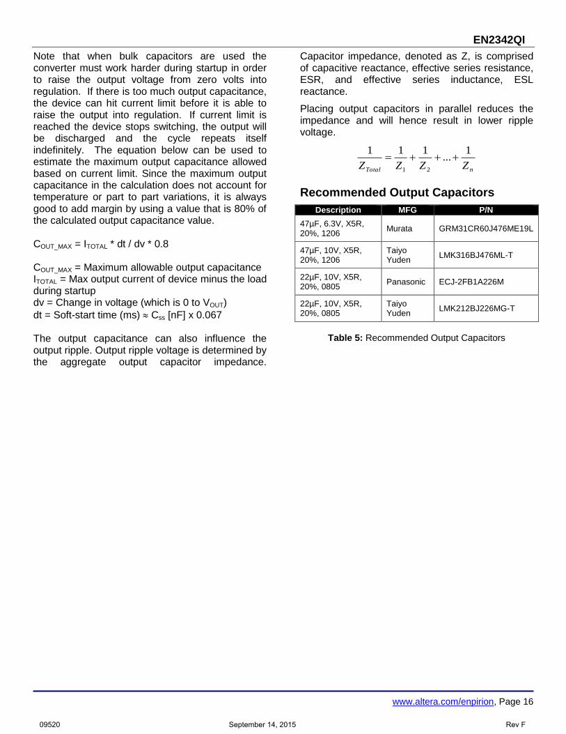
Note that when bulk capacitors are used the converter must work harder during startup in order to raise the output voltage from zero volts into regulation. If there is too much output capacitance, the device can hit current limit before it is able to raise the output into regulation. If current limit is reached the device stops switching, the output will be discharged and the cycle repeats itself indefinitely. The equation below can be used to estimate the maximum output capacitance allowed based on current limit. Since the maximum output capacitance in the calculation does not account for temperature or part to part variations, it is always good to add margin by using a value that is 80% of the calculated output capacitance value. COUT_MAX = ITOTAL * dt / dv * 0.8 COUT_MAX = Maximum allowable output capacitance ITOTAL = Max output current of device minus the load during startup dv = Change in voltage (which is 0 to VOUT)
dt = Soft-start time (ms) Css [nF] x 0.067 The output capacitance can also influence the output ripple. Output ripple voltage is determined by the aggregate output capacitor impedance.
Capacitor impedance, denoted as Z, is comprised of capacitive reactance, effective series resistance, ESR, and effective series inductance, ESL reactance.
Placing output capacitors in parallel reduces the impedance and will hence result in lower ripple voltage.
nTotal ZZZZ
1...
111
21
Recommended Output Capacitors
Description MFG P/N
47µF, 6.3V, X5R, 20%, 1206
Murata GRM31CR60J476ME19L
47µF, 10V, X5R, 20%, 1206
Taiyo Yuden
LMK316BJ476ML-T
22µF, 10V, X5R, 20%, 0805
Panasonic ECJ-2FB1A226M
22µF, 10V, X5R, 20%, 0805
Taiyo Yuden
LMK212BJ226MG-T
Table 5: Recommended Output Capacitors
09520 September 14, 2015 Rev F
EN2342QI
www.altera.com/enpirion, Page 17
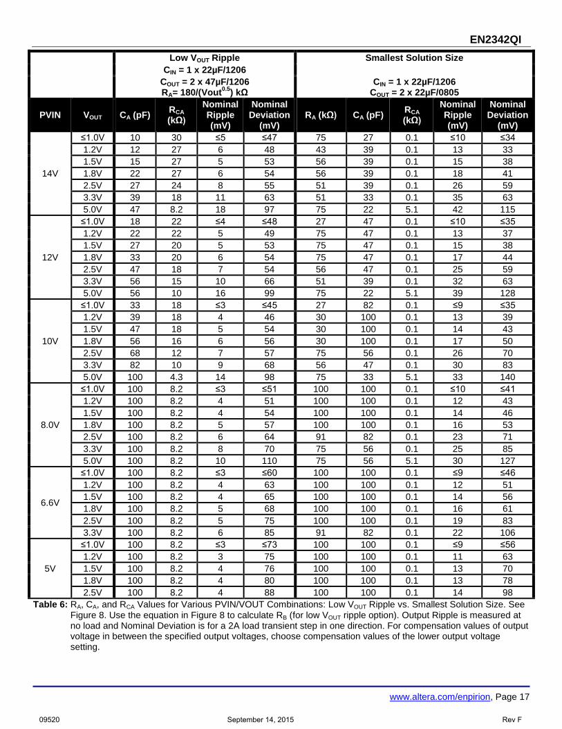
Low VOUT Ripple Smallest Solution Size
CIN = 1 x 22µF/1206
COUT = 2 x 47µF/1206 RA= 180/(Vout
0.5) kΩ
CIN = 1 x 22µF/1206 COUT = 2 x 22µF/0805
PVIN VOUT CA (pF) RCA (kΩ)
Nominal Ripple (mV)
Nominal Deviation
(mV) RA (kΩ) CA (pF)
RCA (kΩ)
Nominal Ripple (mV)
Nominal Deviation
(mV)
14V
≤1.0V 10 30 ≤5 ≤47 75 27 0.1 ≤10 ≤34
1.2V 12 27 6 48 43 39 0.1 13 33
1.5V 15 27 5 53 56 39 0.1 15 38
1.8V 22 27 6 54 56 39 0.1 18 41
2.5V 27 24 8 55 51 39 0.1 26 59
3.3V 39 18 11 63 51 33 0.1 35 63
5.0V 47 8.2 18 97 75 22 5.1 42 115
12V
≤1.0V 18 22 ≤4 ≤48 27 47 0.1 ≤10 ≤35
1.2V 22 22 5 49 75 47 0.1 13 37
1.5V 27 20 5 53 75 47 0.1 15 38
1.8V 33 20 6 54 75 47 0.1 17 44
2.5V 47 18 7 54 56 47 0.1 25 59
3.3V 56 15 10 66 51 39 0.1 32 63
5.0V 56 10 16 99 75 22 5.1 39 128
10V
≤1.0V 33 18 ≤3 ≤45 27 82 0.1 ≤9 ≤35
1.2V 39 18 4 46 30 100 0.1 13 39
1.5V 47 18 5 54 30 100 0.1 14 43
1.8V 56 16 6 56 30 100 0.1 17 50
2.5V 68 12 7 57 75 56 0.1 26 70
3.3V 82 10 9 68 56 47 0.1 30 83
5.0V 100 4.3 14 98 75 33 5.1 33 140
8.0V
≤1.0V 100 8.2 ≤3 ≤51 100 100 0.1 ≤10 ≤41
1.2V 100 8.2 4 51 100 100 0.1 12 43
1.5V 100 8.2 4 54 100 100 0.1 14 46
1.8V 100 8.2 5 57 100 100 0.1 16 53
2.5V 100 8.2 6 64 91 82 0.1 23 71
3.3V 100 8.2 8 70 75 56 0.1 25 85
5.0V 100 8.2 10 110 75 56 5.1 30 127
6.6V
≤1.0V 100 8.2 ≤3 ≤60 100 100 0.1 ≤9 ≤46
1.2V 100 8.2 4 63 100 100 0.1 12 51
1.5V 100 8.2 4 65 100 100 0.1 14 56
1.8V 100 8.2 5 68 100 100 0.1 16 61
2.5V 100 8.2 5 75 100 100 0.1 19 83
3.3V 100 8.2 6 85 91 82 0.1 22 106
5V
≤1.0V 100 8.2 ≤3 ≤73 100 100 0.1 ≤9 ≤56
1.2V 100 8.2 3 75 100 100 0.1 11 63
1.5V 100 8.2 4 76 100 100 0.1 13 70
1.8V 100 8.2 4 80 100 100 0.1 13 78
2.5V 100 8.2 4 88 100 100 0.1 14 98
Table 6: RA, CA, and RCA Values for Various PVIN/VOUT Combinations: Low VOUT Ripple vs. Smallest Solution Size. See Figure 8. Use the equation in Figure 8 to calculate RB (for low VOUT ripple option). Output Ripple is measured at no load and Nominal Deviation is for a 2A load transient step in one direction. For compensation values of output voltage in between the specified output voltages, choose compensation values of the lower output voltage setting.
09520 September 14, 2015 Rev F
EN2342QI
www.altera.com/enpirion, Page 18
Thermal Considerations
Thermal considerations are important power supply design facts that cannot be avoided in the real world. Whenever there are power losses in a system, the heat that is generated by the power dissipation needs to be accounted for. The Altera Enpirion PowerSoC helps alleviate some of those concerns.
The Altera Enpirion EN2342QI DC-DC converter is packaged in an 8x11x3mm 68-pin QFN package. The QFN package is constructed with copper lead frames that have exposed thermal pads. The exposed thermal pad on the package should be soldered directly on to a copper ground pad on the printed circuit board (PCB) to act as a heat sink. The recommended maximum junction temperature for continuous operation is 125°C. Continuous operation above 125°C may reduce long-term reliability. The device has a thermal overload protection circuit designed to turn off the device at an approximate junction temperature value of 150°C.
The EN2342QI is guaranteed to support the full 4A output current up to 85°C ambient temperature. The following example and calculations illustrate the thermal performance of the EN2342QI.
Example:
VIN = 12V
VOUT = 3.3V
IOUT = 4A
First calculate the output power.
POUT = 3.3V x 4A = 13.2W
Next, determine the input power based on the efficiency (η) shown in Figure 9.
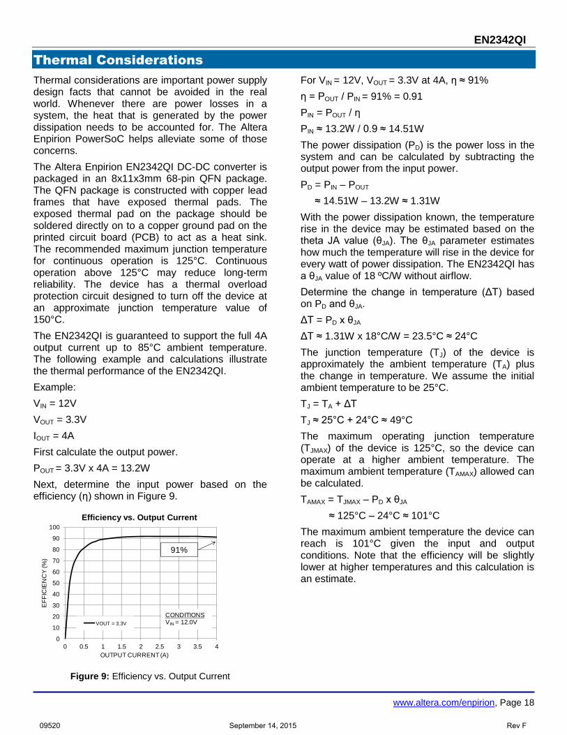
Figure 9: Efficiency vs. Output Current
For VIN = 12V, VOUT = 3.3V at 4A, η ≈ 91%
η = POUT / PIN = 91% = 0.91
PIN = POUT / η
PIN ≈ 13.2W / 0.9 ≈ 14.51W
The power dissipation (PD) is the power loss in the system and can be calculated by subtracting the output power from the input power.
PD = PIN – POUT
≈ 14.51W – 13.2W ≈ 1.31W
With the power dissipation known, the temperature rise in the device may be estimated based on the theta JA value (θJA). The θJA parameter estimates how much the temperature will rise in the device for every watt of power dissipation. The EN2342QI has a θJA value of 18 ºC/W without airflow.
Determine the change in temperature (ΔT) based on PD and θJA.
ΔT = PD x θJA
ΔT ≈ 1.31W x 18°C/W = 23.5°C ≈ 24°C
The junction temperature (TJ) of the device is approximately the ambient temperature (TA) plus the change in temperature. We assume the initial ambient temperature to be 25°C.
TJ = TA + ΔT
TJ ≈ 25°C + 24°C ≈ 49°C
The maximum operating junction temperature (TJMAX) of the device is 125°C, so the device can operate at a higher ambient temperature. The maximum ambient temperature (TAMAX) allowed can be calculated.
TAMAX = TJMAX – PD x θJA
≈ 125°C – 24°C ≈ 101°C
The maximum ambient temperature the device can reach is 101°C given the input and output conditions. Note that the efficiency will be slightly lower at higher temperatures and this calculation is an estimate.
0
10
20
30
40
50
60
70
80
90
100
0 0.5 1 1.5 2 2.5 3 3.5 4
EF
FIC
IEN
CY
(%
)
OUTPUT CURRENT (A)
Efficiency vs. Output Current
VOUT = 3.3V
CONDITIONSVIN = 12.0V
91%
09520 September 14, 2015 Rev F
EN2342QI
www.altera.com/enpirion, Page 19
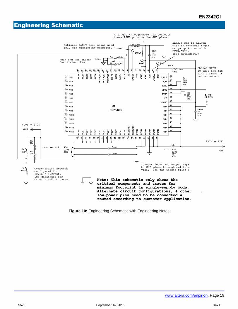
Engineering Schematic
Figure 10: Engineering Schematic with Engineering Notes
09520 September 14, 2015 Rev F
EN2342QI
www.altera.com/enpirion, Page 20
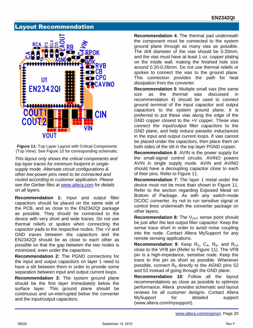
Layout Recommendation
Figure 11: Top Layer Layout with Critical Components (Top View). See Figure 10 for corresponding schematic.
This layout only shows the critical components and top layer traces for minimum footprint in single-supply mode. Alternate circuit configurations & other low-power pins need to be connected and routed according to customer application. Please see the Gerber files at www.altera.com for details on all layers.
Recommendation 1: Input and output filter capacitors should be placed on the same side of the PCB, and as close to the EN2342QI package as possible. They should be connected to the device with very short and wide traces. Do not use thermal reliefs or spokes when connecting the capacitor pads to the respective nodes. The +V and GND traces between the capacitors and the EN2342QI should be as close to each other as possible so that the gap between the two nodes is minimized, even under the capacitors.
Recommendation 2: The PGND connections for the input and output capacitors on layer 1 need to have a slit between them in order to provide some separation between input and output current loops.
Recommendation 3: The system ground plane should be the first layer immediately below the surface layer. This ground plane should be continuous and un-interrupted below the converter and the input/output capacitors.
Recommendation 4: The thermal pad underneath the component must be connected to the system ground plane through as many vias as possible. The drill diameter of the vias should be 0.33mm, and the vias must have at least 1 oz. copper plating on the inside wall, making the finished hole size around 0.20-0.26mm. Do not use thermal reliefs or spokes to connect the vias to the ground plane. This connection provides the path for heat dissipation from the converter.
Recommendation 5: Multiple small vias (the same size as the thermal vias discussed in recommendation 4) should be used to connect ground terminal of the input capacitor and output capacitors to the system ground plane. It is preferred to put these vias along the edge of the GND copper closest to the +V copper. These vias connect the input/output filter capacitors to the GND plane, and help reduce parasitic inductances in the input and output current loops. If vias cannot be placed under the capacitors, then place them on both sides of the slit in the top layer PGND copper.
Recommendation 6: AVIN is the power supply for the small-signal control circuits. AVINO powers AVIN in single supply mode. AVIN and AVINO should have a decoupling capacitor close to each of their pins. Refer to Figure 11.
Recommendation 7: The layer 1 metal under the device must not be more than shown in Figure 11. Refer to the section regarding Exposed Metal on Bottom of Package. As with any switch-mode DC/DC converter, try not to run sensitive signal or control lines underneath the converter package on other layers.
Recommendation 8: The VOUT sense point should be just after the last output filter capacitor. Keep the sense trace short in order to avoid noise coupling into the node. Contact Altera MySupport for any remote sensing applications.
Recommendation 9: Keep RA, CA, RB, and RCA close to the VFB pin (Refer to Figure 11). The VFB pin is a high-impedance, sensitive node. Keep the trace to this pin as short as possible. Whenever possible, connect RB directly to the AGND pins 52 and 53 instead of going through the GND plane.
Recommendation 10: Follow all the layout recommendations as close as possible to optimize performance. Altera provides schematic and layout reviews for all customer designs. Contact Altera MySupport for detailed support (www.altera.com/mysupport).
09520 September 14, 2015 Rev F

EN2342QI
www.altera.com/enpirion, Page 21
Design Considerations for Lead-Frame Based Modules
Exposed Metal on Bottom of Package
Lead-frames offer many advantages in thermal performance, in reduced electrical lead resistance, and in overall foot print. However, they do require some special considerations.
In the assembly process lead frame construction requires that, for mechanical support, some of the lead-frame cantilevers be exposed at the point where wire-bond or internal passives are attached. This results in several small pads being exposed on the bottom of the package, as shown in Figure 12.
Only the thermal pad and the perimeter pads are to be mechanically or electrically connected to the PC board. The PCB top layer under the EN2342QI should be clear of any metal (copper pours, traces, or vias) except for the thermal pad. The “shaded-out” area in Figure 12 represents the area that should be clear of any metal on the top layer of the PCB. Any layer 1 metal under the shaded-out area runs the risk of undesirable shorted connections even if it is covered by soldermask.
The solder stencil aperture should be smaller than the PCB ground pad. This will prevent excess solder from causing bridging between adjacent pins or other exposed metal under the package. Please consult the Enpirion Manufacturing Application Note for more details and recommendations.
Figure 12: Lead-Frame exposed metal (Bottom View)
Shaded area highlights exposed metal that is not to be mechanically or electrically connected to the PCB.
09520 September 14, 2015 Rev F
EN2342QI
www.altera.com/enpirion, Page 22
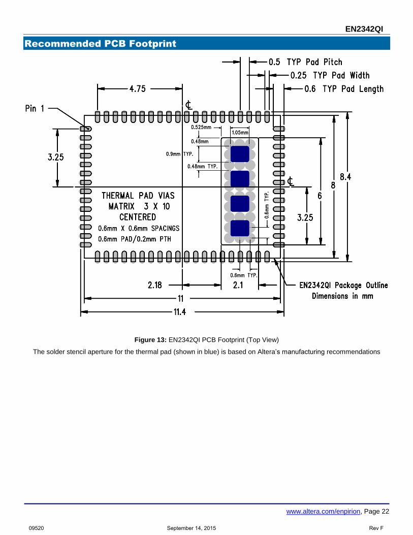
Recommended PCB Footprint
Figure 13: EN2342QI PCB Footprint (Top View)
The solder stencil aperture for the thermal pad (shown in blue) is based on Altera’s manufacturing recommendations
09520 September 14, 2015 Rev F

EN2342QI
www.altera.com/enpirion, Page 23
Package and Mechanical
Figure 14: EN2342QI Package Dimensions (Bottom View)
Packing and Marking Information: www.altera.com/support/reliability/packing/rel-packing-and-marking.html
Contact Information
Altera Corporation 101 Innovation Drive San Jose, CA 95134 Phone: 408-544-7000 www.altera.com
© 2014 Altera Corporation—Confidential. All rights reserved. ALTERA, ARRIA, CYCLONE, ENPIRION, HARDCOPY, MAX, MEGACORE, NIOS, QUARTUS and STRATIX words and logos are trademarks of Altera Corporation and registered in the U.S. Patent and Trademark Office and in other countries. All other words and logos identified as trademarks or service marks are the property of their respective holders as described at www.altera.com/common/legal.html. Altera warrants performance of its semiconductor
products to current specifications in accordance with Altera's standard warranty, but reserves the right to make changes to any products and services at any time without notice. Altera assumes no responsibility or liability arising out of the application or use of any information, product, or service described herein except as expressly agreed to in writing by Altera. Altera customers are advised to obtain the latest version of device specifications before relying on any published information and before placing orders for products or services.
09520 September 14, 2015 Rev F