eee1012 introduction to electrical & electronics engineering chapter 6: bipolar junction...
TRANSCRIPT

EEE1012Introduction to Electrical &
Electronics EngineeringChapter 6: Bipolar Junction Transistor
by Muhazam Mustapha, September 2010
Learning Outcome
• Be able to explain some basic physical theory and operation of BJT
• Be able to do calculation on DC and AC analysis on BJT circuit
By the end of this chapter students are expected to:
Chapter Content
• Theory of BJT
• BJT Operation
• DC Analysis
• AC Analysis

Bipolar Junction Transistor
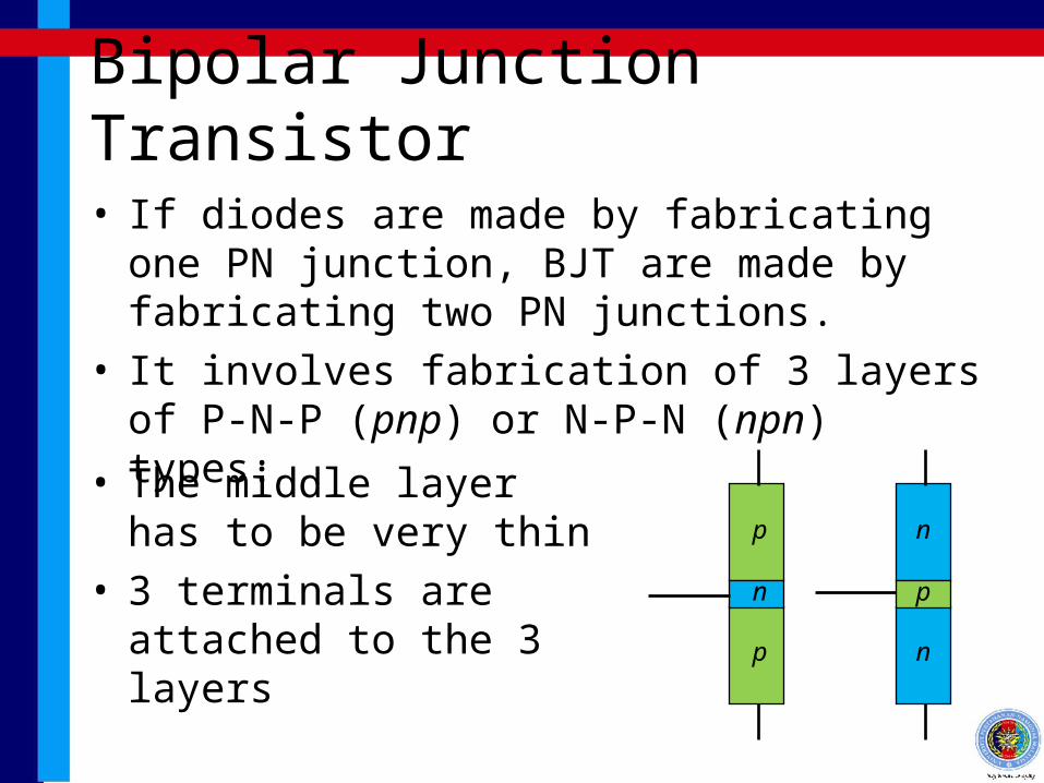
Bipolar Junction Transistor
• If diodes are made by fabricating one PN junction, BJT are made by fabricating two PN junctions.
• It involves fabrication of 3 layers of P-N-P (pnp) or N-P-N (npn) types:
p
p
n
n
n
p
• The middle layer has to be very thin
• 3 terminals are attached to the 3 layers
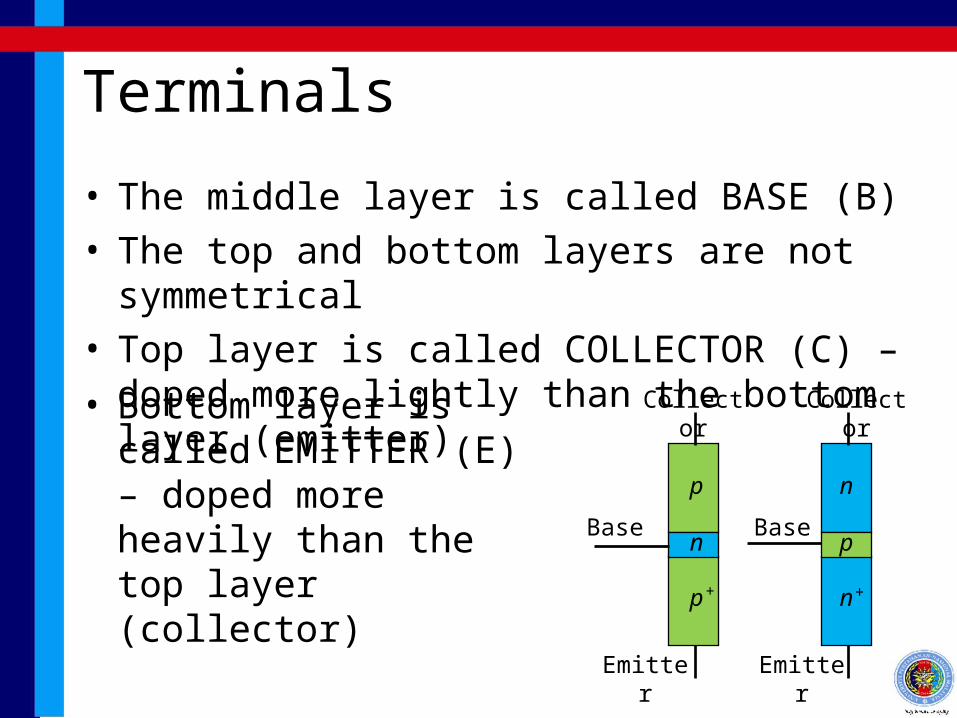
Terminals
• The middle layer is called BASE (B)• The top and bottom layers are not symmetrical• Top layer is called COLLECTOR (C) – doped
more lightly than the bottom layer (emitter)Collector
p
n
n
n
p
• Bottom layer is called EMITTER (E) – doped more heavily than the top layer (collector)
Collector
EmitterEmitter
BaseBase
p
+ +

Circuit Symbol and Notations
• npn BJT symbol: • pnp BJT symbol:C C
E E
B B
• The direction of the arrow is the direction of the current when the BE junction is put on forward bias
C C
E E
B B
Circuit Symbol and Notations
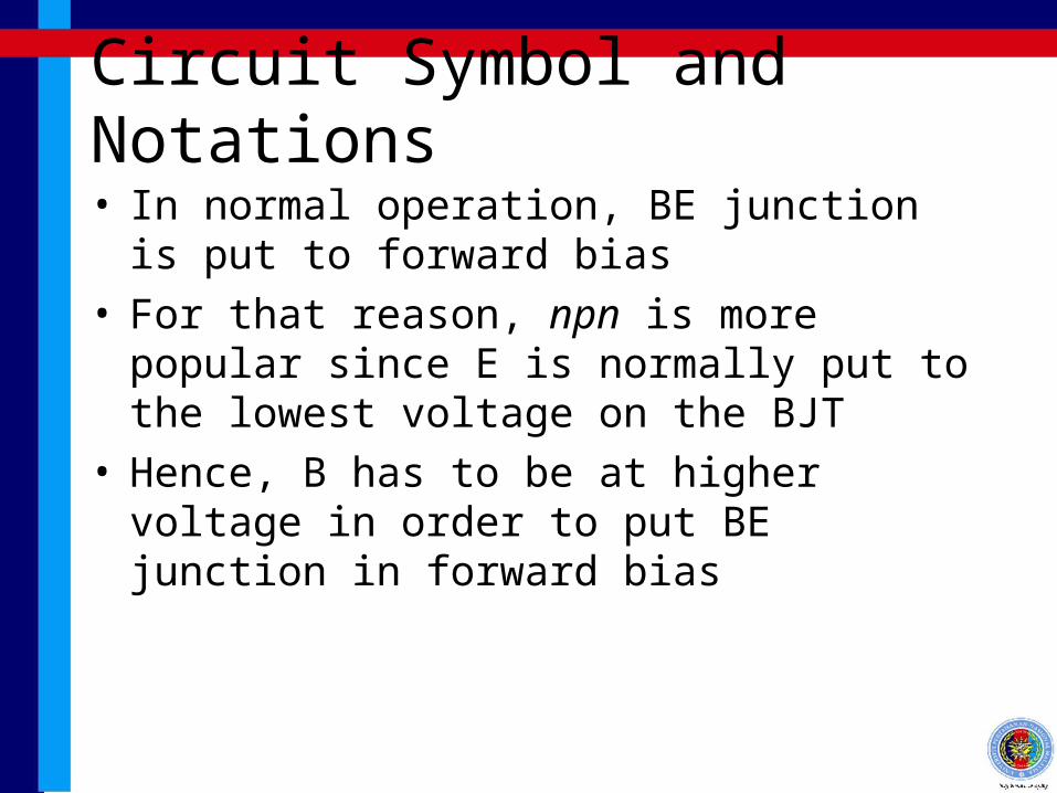
• In normal operation, BE junction is put to forward bias
• For that reason, npn is more popular since E is normally put to the lowest voltage on the BJT
• Hence, B has to be at higher voltage in order to put BE junction in forward bias

Circuit Symbol and Notations• Notation for currents and voltage for npn:
C
E
B
iB
iC
iE
vCE
+
−
vCB
+
−
vBE
+
−
KCL: iE = iB + iC
KVL: vCE = vCB + vBE
• For pnp, the polarities are reversed
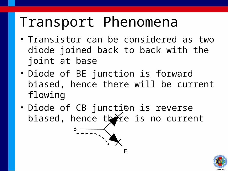
Transport Phenomena• Transistor can be considered as two diode
joined back to back with the joint at base• Diode of BE junction is forward biased, hence
there will be current flowing• Diode of CB junction is reverse biased, hence
there is no currentC
E
B

Transport Phenomena• So how do we get current flowing through C?• Current manages to get through C due to the
fact that B layer is very thin• Since B layer is very thin, the reversely flowing
transport (electron or hole) at BE junction will overshoot into the depletion region on the reverse biased CB junction

Transport Phenomena
P
N
N
hole movement
forward biased electron movement
overshooting electrons across reverse biased junction causing large avalanche current

Transport Phenomena• These overshot transport will further collide with
the covalence bond in depletion region and produce more holes and electrons
• The newly produced electrons and holes will further collide with other bonds and produce more and more new free electrons and holes
• The whole process explained above is called avalanche
• These avalanche produced electrons and holes will too move under the influence of the external field (voltage of vCE)
Transport Phenomena• Hence the current through C (iC) is contributed
by the overshooting and avalanched transport
• Since the overshooting current is due to iB, and since the amount of the avalanche current is due to the overshooting current, then the amount of avalanche current would be proportional to iB
• So as to say, iB actually controls iC by some multiplication factor
• This factor is called the CURRENT GAIN, β

I-V Characteristic• Since iC can be controlled by iB, we can consider
BJT like an input-output transfer box• The current and voltage input parameter of BJT
are iB and vBE respectively
• While the current and voltage output parameter of BJT are iC and vCE respectively
• The I-V characteristic of BJT is featured by the I-V characteristics of these input and output
C
E
B
iB
iC
vCE
+
−vBE
+
−
OU
TP
UTIN
PU
T
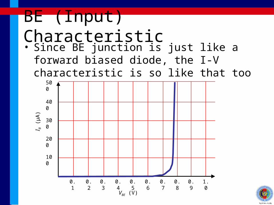
BE (Input) Characteristic• Since BE junction is just like a forward biased
diode, the I-V characteristic is so like that too
500
400
300
200
100
0.1 0.2 0.3 0.4 0.5 0.6 0.7 0.8 0.9 1.0
I B (
μA
)
VBE (V)

CE (Output) Characteristic• Since CB junction is reversed biased, the I-V
characteristic of CE is flat (zero) unless IB > 0
• With some values of IB, we get a family of I-V flattening curves for CE
50
40
30
20
10
1 2 3 4 5 6 7 8 9 10
I C (
mA
)
VCE (V)
IB = 50μA
IB = 100μA
IB = 150μA
IB = 200μA
IB = 250μA
IB = 300μA
IB = 0
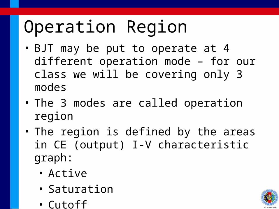
Operation Region• BJT may be put to operate at 4 different
operation mode – for our class we will be covering only 3 modes
• The 3 modes are called operation region• The region is defined by the areas in CE
(output) I-V characteristic graph:• Active• Saturation• Cutoff
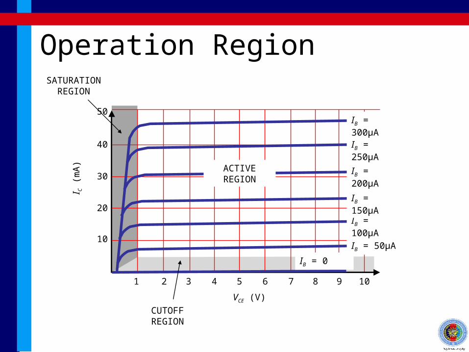
Operation Region
50
40
30
20
10
1 2 3 4 5 6 7 8 9 10
I C (
mA
)
VCE (V)
IB = 50μA
IB = 100μA
IB = 150μA
IB = 200μA
IB = 250μA
IB = 300μA
IB = 0
CUTOFF REGION
SATURATION REGION
ACTIVE REGION

Cutoff State / Region• The BJT is basically in OFF condition with no
current flowing because IB is zero
• Uses:• OFF state in digital circuit• OFF state for analog switch
• Detailed features:
• IB = 0
• IC = ICEO ≈ 0
• VCE ≥ 0
• VBE < VD

Saturation State / Region• The BJT is basically in full ON condition with
very low VCE whereby the BJT may be considered to have a very low output resistance
• Uses:• ON state in digital circuit• ON state for analog switch
• Detailed features:
• IB > 0
• IC < βIB
• VCE = Vsat ≈ 0.2V
• VBE = VD
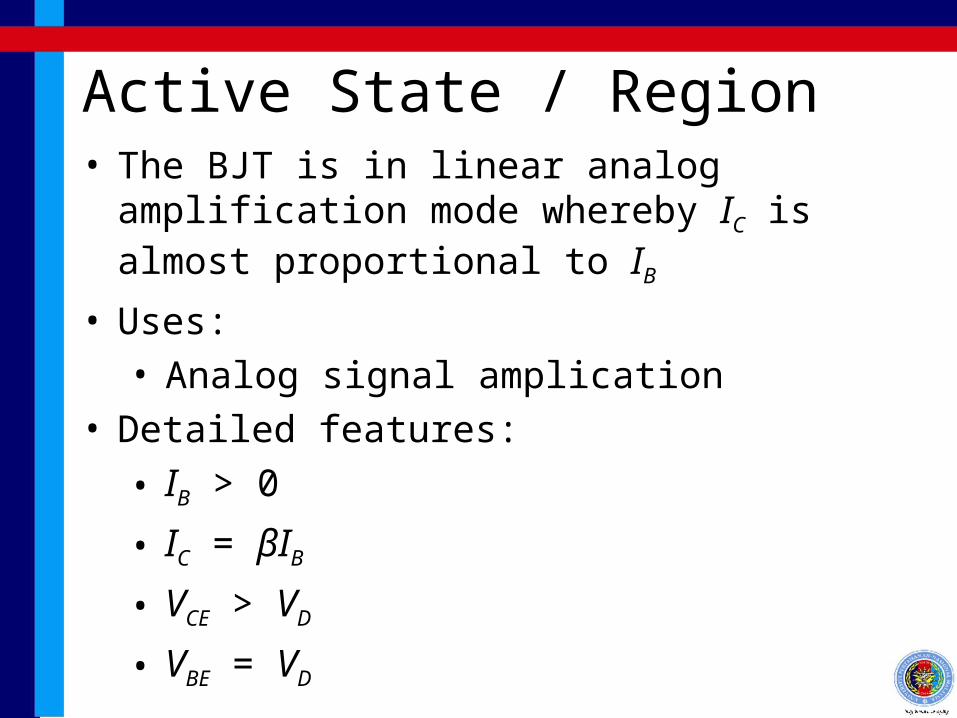
Active State / Region• The BJT is in linear analog amplification mode
whereby IC is almost proportional to IB
• Uses:• Analog signal amplication
• Detailed features:
• IB > 0
• IC = βIB
• VCE > VD
• VBE = VD
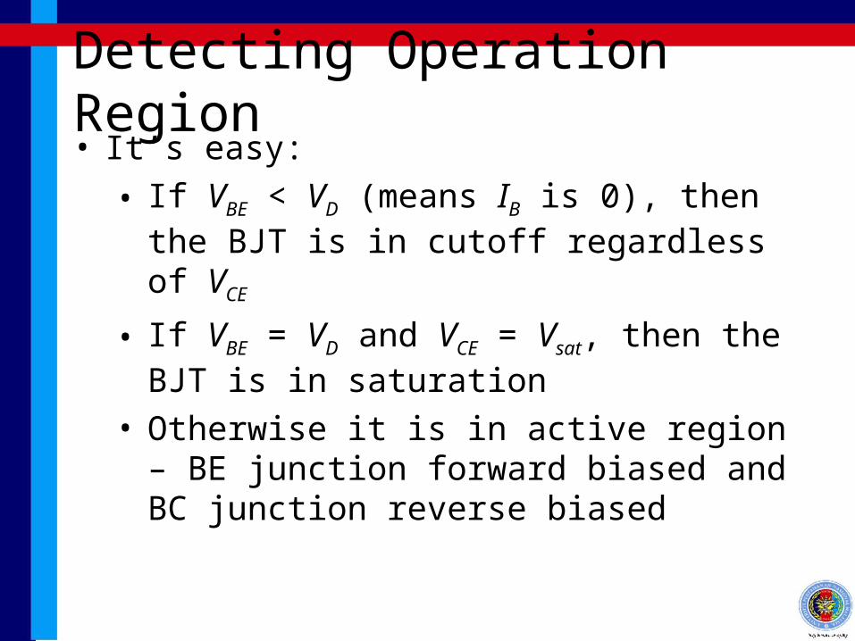
Detecting Operation Region• It’s easy:
• If VBE < VD (means IB is 0), then the BJT is in cutoff regardless of VCE
• If VBE = VD and VCE = Vsat, then the BJT is in saturation
• Otherwise it is in active region – BE junction forward biased and BC junction reverse biased
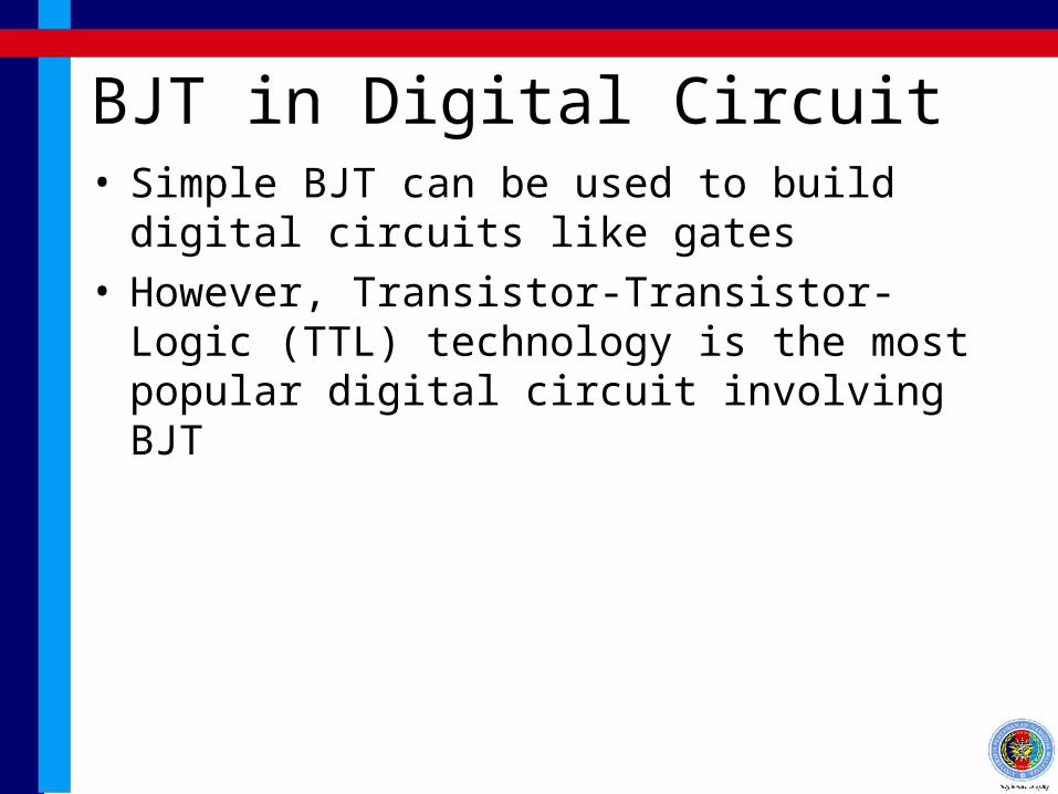
BJT in Digital Circuit• Simple BJT can be used to build digital circuits
like gates• However, Transistor-Transistor-Logic (TTL)
technology is the most popular digital circuit involving BJT
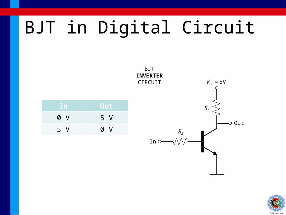
BJT in Digital Circuit
VCC = 5V
Out
In
RB
RC
BJT INVERTER CIRCUIT
In Out
0 V 5 V
5 V 0 V
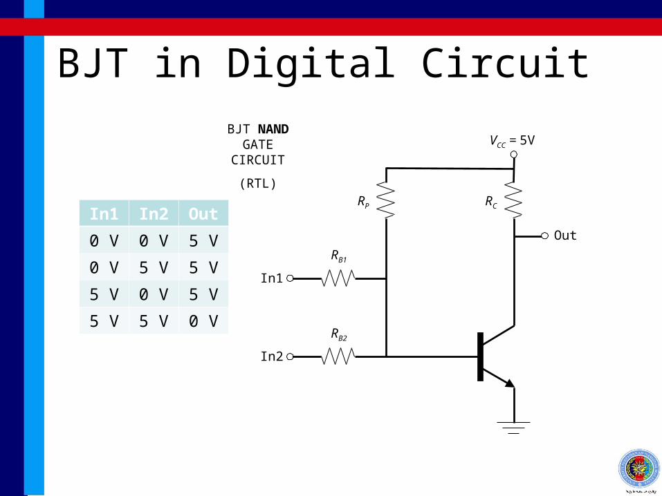
BJT in Digital Circuit
VCC = 5V
Out
In1
RB1
RC
BJT NAND GATE
CIRCUIT
(RTL)
In1 In2 Out
0 V 0 V 5 V
0 V 5 V 5 V
5 V 0 V 5 V
5 V 5 V 0 V
In2
RB2
RP
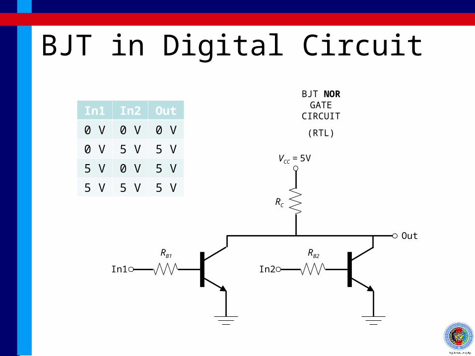
BJT in Digital Circuit
VCC = 5V
Out
In1
RB1
RC
BJT NOR GATE
CIRCUIT
(RTL)
In1 In2 Out
0 V 0 V 0 V
0 V 5 V 5 V
5 V 0 V 5 V
5 V 5 V 5 V
In2
RB2

Biasing (DC Analysis)
DC Analysis (Biasing)
• Biasing of a transistor means putting the transistor’s VCE and IC into a desired position in the IC-VCE graph
• This is done normally if we want the transistor to operate in active region
• Cutoff and saturation region normally don’t require much biasing since the area is limited
• The biasing process is a little tricky since IC is controlled by IB – not directly by VCE
Refer to Giorgio Rizzoni’s Fundamentals of Electrical Engineering: Chapter 10.4, Example 10.7, Example 10.9
DC Analysis (Biasing)
• The position of the biased BJT’s VCE and IC is called Q point
• The value of IB is also required for the biasing
• There are a few biasing configuration exist, but for the purpose of non-EE class, we will only study the most popular configuration called self-bias common emitter configuration– Refer to Giorgio Rizzoni’s Fundamentals of Electrical
Engineering Figure 10.26
Refer to Giorgio Rizzoni’s Fundamentals of Electrical Engineering: Chapter 10.4, Example 10.7, Example 10.9
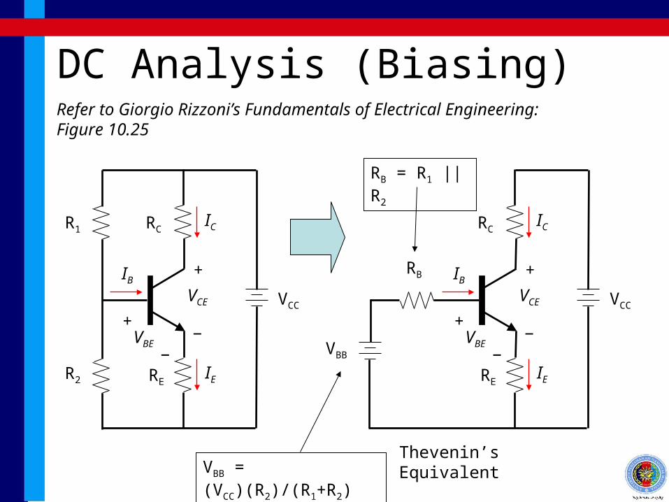
DC Analysis (Biasing)Refer to Giorgio Rizzoni’s Fundamentals of Electrical Engineering: Figure 10.25
R2
R1
VCC
RC
RE
IB
IC
VCE
+
−VBE
+
−IE
RB
VCC
RC
RE
IB
IC
VCE
+
−VBE
+
−IE
VBB
Thevenin’s EquivalentVBB = (VCC)(R2)/(R1+R2)
RB = R1 || R2
DC Analysis (Biasing)
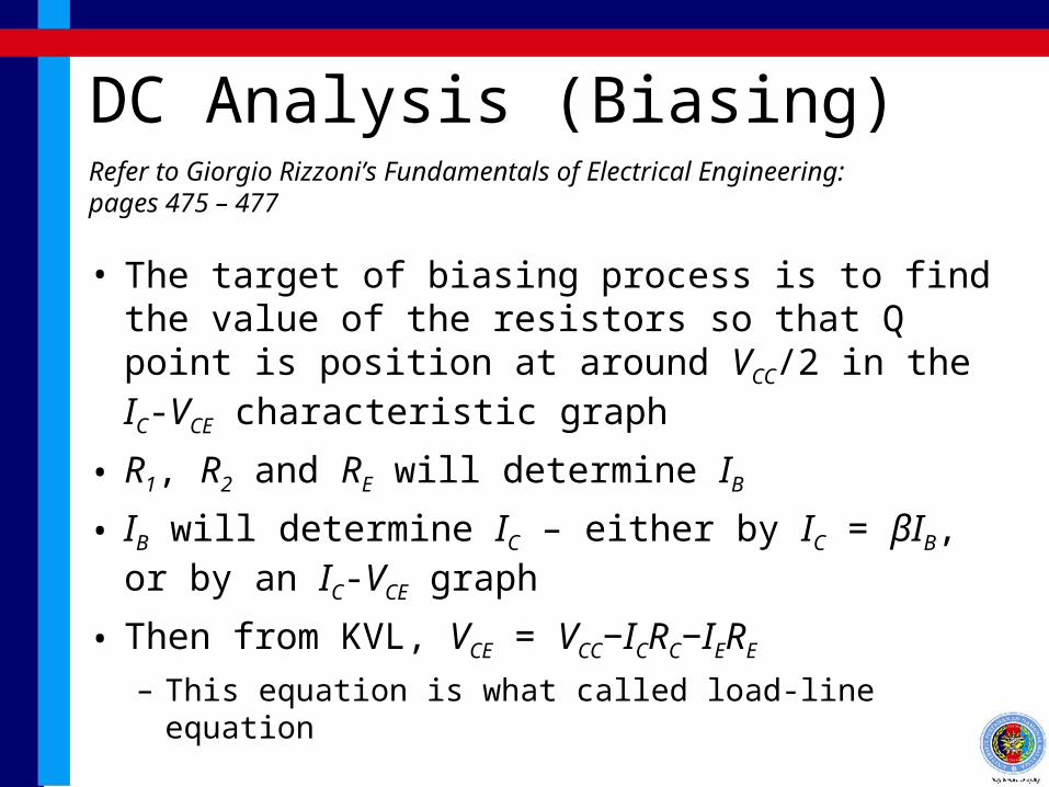
• The target of biasing process is to find the value of the resistors so that Q point is position at around VCC/2 in the IC-VCE characteristic graph
• R1, R2 and RE will determine IB
• IB will determine IC – either by IC = βIB, or by an IC-VCE graph
• Then from KVL, VCE = VCC−ICRC−IERE
– This equation is what called load-line equation
Refer to Giorgio Rizzoni’s Fundamentals of Electrical Engineering: pages 475 – 477
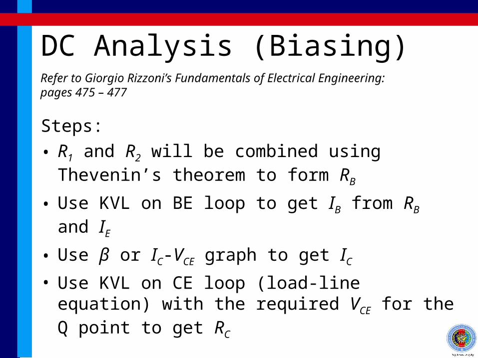
DC Analysis (Biasing)
Steps:
• R1 and R2 will be combined using Thevenin’s theorem to form RB
• Use KVL on BE loop to get IB from RB and IE
• Use β or IC-VCE graph to get IC
• Use KVL on CE loop (load-line equation) with the required VCE for the Q point to get RC
Refer to Giorgio Rizzoni’s Fundamentals of Electrical Engineering: pages 475 – 477

DC Analysis (Biasing)
• Class discussion: Giorgio Rizzoni’s Fundamentals of Electrical Engineering: pages 475 – 477, Example 10.9
AC Analysis

AC Analysis
• AC analysis is done to determine the performance of transistor amplifier circuit
• There are a few parameters of interest, like input and output resistance, but for the purpose of non-EE class, we will do only AC gain (current and voltage)
• AC analysis is done after biasing is completed and assuming there is some AC signal being introduced into the circuit as superimpose on top of the DC values (biasing)
Refer to Giorgio Rizzoni’s Fundamentals of Electrical Engineering: Example 10.8, page 472-475
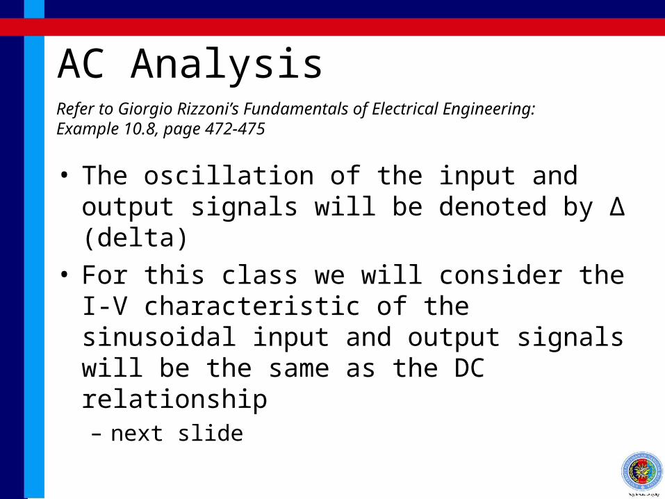
AC AnalysisRefer to Giorgio Rizzoni’s Fundamentals of Electrical Engineering: Example 10.8, page 472-475
• The oscillation of the input and output signals will be denoted by Δ (delta)
• For this class we will consider the I-V characteristic of the sinusoidal input and output signals will be the same as the DC relationship– next slide

AC AnalysisRefer to Giorgio Rizzoni’s Fundamentals of Electrical Engineering: Example 10.8, page 472-475
R2
R1
VCC
RC
RE
ΔVB
ΔVO
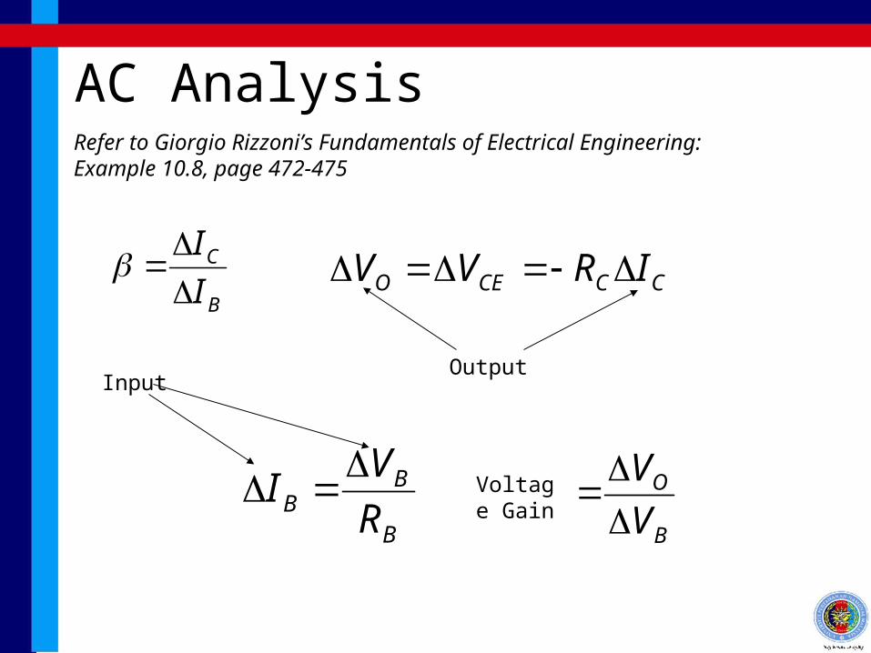
AC AnalysisRefer to Giorgio Rizzoni’s Fundamentals of Electrical Engineering: Example 10.8, page 472-475
B
C
I
I
CCCEO IRVV
B
BB R
VI
OutputInput
Voltage Gain
B
O
V
V

ΔVO FormulaRefer to Giorgio Rizzoni’s Fundamentals of Electrical Engineering: Example 10.8, page 472-475
R2
R1
VCC
RC
RE
ΔVB
ΔVO
In the formula for ΔVO, it only depends on ΔIC even though from the KVL at the output it should also depends on ΔIE.
The reason for this is in real circuit we put a capacitor across RE which effectively SHORTS circuit RE when AC current flows – means we can disregard RE in AC analysis formula.

AC Analysis
• Class discussion: Giorgio Rizzoni’s Fundamentals of Electrical Engineering: pages 473 – 475, Example 10.8