eecs 452 lab 3—introduction to the de2-70 fpga board · eecs 452 lab 3—introduction to the...
TRANSCRIPT

EECS 452 Lab 3—Introduction to the DE2-70 FPGA board
EECS 452 Lab 3—Introduction to the DE2-70 FPGA board
The purposes of this lab are to:
• Provide an introduction to the DE2-70 FPGA(the board will be used for the rest of the course in conjunction with the C5515)
• Provide an introduction to Verilog (a hardware description language) • Revisit DDS in hardware
outputting to audio and VGA
In addition, you will gain familiarity with Altera’s Quartus, the software that interfaces with the FPGA and the various forms of documentation and sample code that comes with this platform.
1. Background Material There is quite a bit of material you’ll want
to understand before you start working on this lab. All answers should be typed though neat drawings will be accepted when figures are required.
Programming The rest of the labs will require you to be familiar with the hardware description language Verilog. If
you have not taken EECS 270, this lab is meant to get you up to speed. If you have taken EECS 270 or an equivalent class this lab should be mostly review though some new ideas are introduced.
2. Pre-lab The pre-lab is designed to get you up to speed on basic combinational logic, sequential logic and
Verilog syntax. If you’ve had EECS 270 this should be fairly trivial. If you’ve never worked with digital logic before, you should expect to spend 3-4 hours on this pre-lab. We’d strongly suggest you read a quick tutorial. http://www.play-hookey.com/digital/ has a decent fast introduction though it isn’t anywhere near as complete or formal as a text such as Vahid or Wakerly (both of which are solid books though Vahid is probably a better book to learn from and Wakerly is a better reference). There is also a fairly short book on-line (well short as books go) that provides a fairly quick and solid background at the University of Oregon http://pages.uoregon.edu/rayfrey/DigitalNotes.pdf. Sections 2.1, 3.2.1, 4.3 and 6 would be plenty. Everyone might find Section 5 to be a nice introduction to A/D converters (which we will be using during the semester).
Figure 1: The DE2-70 FPGA board
Version V14.2, 9/28/2014 9:14 PM Page 1 of 16

EECS 452 Lab 3—Introduction to the DE2-70 FPGA board
Review of combinational logic Combinational logic is a type of logic where the output is purely determined by the current input.
This is in contrast to sequential logic where the output also depends on previous inputs. In this document we will generally use the asterisk * as AND, the plus + as OR, a single tick ‘ as negation and a circled-plus ⊕ as XOR.
Q1. Consider the logic statement (A*B)+(C*A’)
a. Write the truth table for that logic statement b. Draw the gates that implement that logic statement (without simplification).
Q2. Consider a 2-to-1 MUX as drawn on the right. a. Write a truth table for this circuit. b. Using standard 2-input gates (AND, OR, XOR) and the NOT
gate, draw a circuit which implements the same function (has the same truth table).
Q3. Consider a full-adder as drawn on the right. a. Write a truth table for this circuit. b. Using standard 2-input gates (AND, OR, XOR) and the
NOT gate, draw a circuit which implements the same function (has the same truth table).
Now may need to read the combinational logic tutorial for Verilog
found on our course website (it is on the lab page with the other lab3 information.) It is taken from EECS 270. Answer the following questions about implementing combinational logic in Verilog.
Q4. Using an assign statement, implement the following
(including declaring all outputs) a. X=(A*B)+C’+(B*D)’ b. The logic to implement the 2-to-1 MUX. Use A, B, Se as the inputs and Z as the output.
Q5. Using the adder in the tutorial as a template, implement a. A module implementing a 2-to-1 MUX called MUX21 which takes three inputs (A,B,S)
and generates one output (Z). b. A module implementing a 4-to-1 MUX called MUX41 which takes 6 bits of input (A[3:0],
S[1:0]) and generates one output (Z). It should do all its work by instantiating the 2-to-1 MUX of part a.
c. A module implementing a 4-to-2 MUX called MUX42 which takes 5 bits of input (A[1:0], B[1:0], S) and generates two bits of output (Z[1:0]). It should do all its work by instantiating the 2-to-1 MUX of part a.
In addition to assign statements, combinational logic can be implemented in an “always @*” block. Q6. Redo problem Q4.a using an always @* block.
Review of Sequential logic Sequential logic revolves around storage elements. There are a number of different types of storage
elements, but for the most part digital designers use only one: the D flip-flop. It’s a device that has two
Version V14.2, 9/28/2014 9:14 PM Page 2 of 16
EECS 452 Lab 3—Introduction to the DE2-70 FPGA board
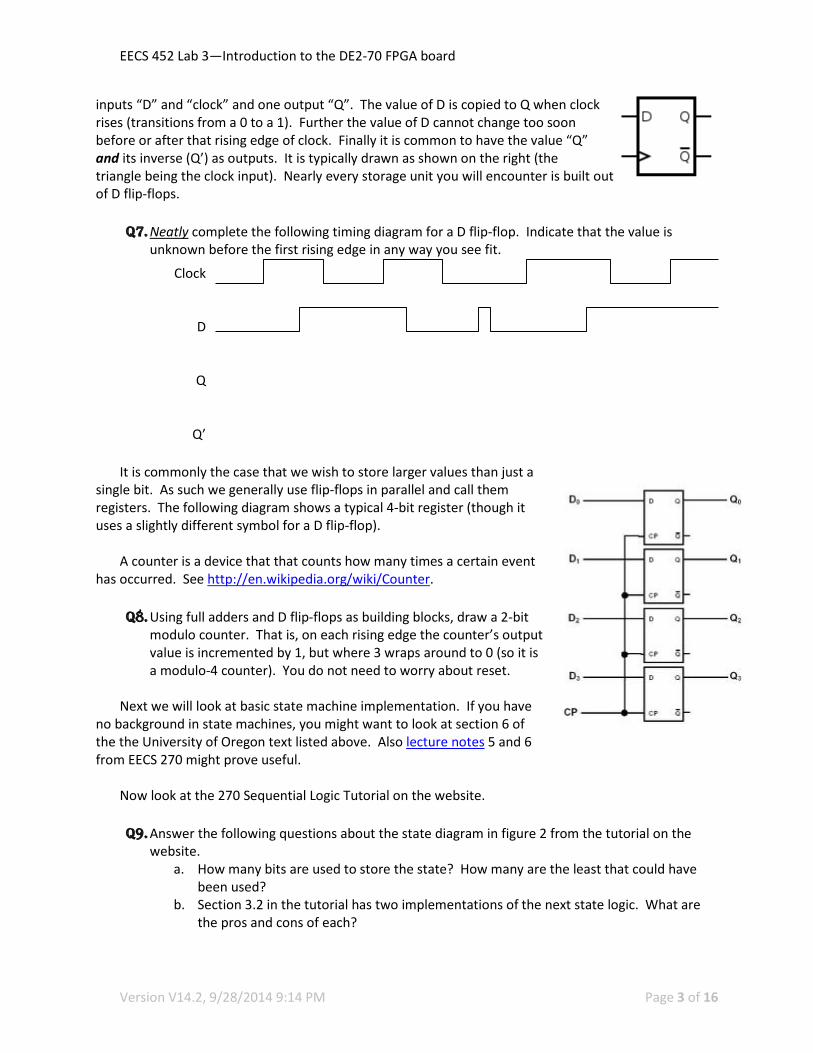
inputs “D” and “clock” and one output “Q”. The value of D is copied to Q when clock rises (transitions from a 0 to a 1). Further the value of D cannot change too soon before or after that rising edge of clock. Finally it is common to have the value “Q” and its inverse (Q’) as outputs. It is typically drawn as shown on the right (the triangle being the clock input). Nearly every storage unit you will encounter is built out of D flip-flops.
Q7. Neatly complete the following timing diagram for a D flip-flop. Indicate that the value is
unknown before the first rising edge in any way you see fit.
It is commonly the case that we wish to store larger values than just a
single bit. As such we generally use flip-flops in parallel and call them registers. The following diagram shows a typical 4-bit register (though it uses a slightly different symbol for a D flip-flop).
A counter is a device that that counts how many times a certain event
has occurred. See http://en.wikipedia.org/wiki/Counter. Q8. Using full adders and D flip-flops as building blocks, draw a 2-bit
modulo counter. That is, on each rising edge the counter’s output value is incremented by 1, but where 3 wraps around to 0 (so it is a modulo-4 counter). You do not need to worry about reset.
Next we will look at basic state machine implementation. If you have no background in state machines, you might want to look at section 6 of the the University of Oregon text listed above. Also lecture notes 5 and 6 from EECS 270 might prove useful.
Now look at the 270 Sequential Logic Tutorial on the website. Q9. Answer the following questions about the state diagram in figure 2 from the tutorial on the
website. a. How many bits are used to store the state? How many are the least that could have
been used? b. Section 3.2 in the tutorial has two implementations of the next state logic. What are
the pros and cons of each?
Clock
D
Q
Q’
4-bit register, from http://cpuville.com/register.htm
Version V14.2, 9/28/2014 9:14 PM Page 3 of 16

EECS 452 Lab 3—Introduction to the DE2-70 FPGA board
Q10. Draw the state transition diagram which is implemented by the following code. Your diagram should resemble figure 2a from the tutorial. You need not include reset. module statem(clk, in, reset, out); input clk, in, reset; output [3:0] out; reg [3:0] out; reg [1:0] state; reg [1:0] next_state; parameter zero=2'd0, one=2'd1, two=2'd2, three=2'd3; always @* begin case (state) zero: begin out = 4'b0000; next_state = one; end one: begin out = 4'b0001; if(in) next_state = one; else next_state = two; end two: begin out = 4'b0010; if(in) next_state = one; else next_state = three; end three: begin out = 4'b0100; next_state = zero; end default: begin out = 4'b0000; next_state = zero; end endcase end always @(posedge clk) begin if (reset) state <= zero; else state <= next_state; end endmodule
Version V14.2, 9/28/2014 9:14 PM Page 4 of 16

EECS 452 Lab 3—Introduction to the DE2-70 FPGA board
Consider the following Verilog module. It is to take in a 4-bit number (“in”) and convert it for use on a 7-segment display. As the 4-bit numbers can range from “0” to “15” the display should display them in hex, “0” to “F”. For example, looking at the figure to the right, for “0” we’d want segment 6 off and the rest on. Because the hex outputs are “active low” (they turn on when driven with a low value) we’d write that as 7’b1000000 (the 7’b means it’s a 7-bit value, written in binary). Note, you could also write it as 7’d64 (7-bit value, written in decimal) or 7’h40.
module SevenSegmentDisplayDecoder(in, ssOut); input [3:0] in; output reg [6:0] ssOut; always @* case (in) 4'h0: ssOut = 7'b1000000; 4'h1: ssOut = ___________ 4'h2: ssOut = ___________; 4'h3: ssOut = ___________; 4'h4: ssOut = ___________; 4'h5: ssOut = 7'b0010010; 4'h6: ssOut = ___________; 4'h7: ssOut = 7'b1111000; 4'h8: ssOut = ___________; 4'h9: ssOut = 7'b0011000; 4'hA: ssOut = ___________; 4'hB: ssOut = 7'b0000011; 4'hC: ssOut = 7'b1000110; 4'hD: ssOut = 7'b0100001; 4'hE: ssOut = ___________; 4'hF: ssOut = ___________; endcase endmodule
Q11. Consider the above Verilog code and respond to the questions/requests below.
a. Provide the above code with the blanks correctly filled in. b. At present the values for the hex displays are listed in binary while the labels for the
case statements are in hex. Why do you think that was done?
Generate a SINE table using MATLAB for verilog You will want to use C or Matlab to generate your sine table. You might find the following bit of
Matlab helpful in formatting the output. It assumes your sine table (in Q15) is in an array named “x”. Feel free to either do the formatting by hand or however else you wish, the code below is just there if you want to use it.
for b=0:63 fprintf('\t\t\t%2d : dataOut <= %d;\n',b,round(x(b+1))) end
Version V14.2, 9/28/2014 9:14 PM Page 5 of 16

EECS 452 Lab 3—Introduction to the DE2-70 FPGA board
Sawtooth Synthesis We know that we can use the Fourier series to generate different waves from a sine table. In lab 2
we used DDS to generate sine waves. Now, you will use a sine table to generate a sawtooth1 output using at least 4 sine waves. In the lab, your output will be to the VGA and you are to display about two full periods of the sawtooth.
On the course website (in lab3_Files.zip) you will find a very useful MATLAB program that generates
2 periods of a sawtooth wave using the first four sine waves in the Fourier series. This code also keeps the output between 150 and 350 so it fits nicely on the screen (the screen actually is larger than that though…).
Strive to understand the MATLAB code. It was designed to work in fixed point and to closely
correspond to the fixed point values you’ll use in your Verilog code. It also implements a MATLAB version of DDS that uses the same structure as you coded in lab2.
Q12. Fill in the blank in the MATLAB code.
a. What would be the code to calculate the FTV for each sinusoid b. Write down the FTV values you calculated for this set-up of the code
Your code should generate a plot that is very similar to the figure below.
Q13. Change the order of your Fourier synthesis to 20 and attach the plot to your pre-lab report.
1 See http://mathworld.wolfram.com/FourierSeriesSawtoothWave.html
Version V14.2, 9/28/2014 9:14 PM Page 6 of 16

EECS 452 Lab 3—Introduction to the DE2-70 FPGA board
3. In-Lab The In-lab is broken into two parts. The first part is about getting familiar with Verilog, Quartus and
our FPGA board. You will download, modify and write some fairly simple projects involving the switches and LEDs on the board. The second part will give you some experience with signal generation and output to a monitor (VGA) and an audio output. The DSP material will be built upon in the next lab assignment.
Download the Lab 3 files from the Ctools.
Section A: Getting familiar with Verilog and Quartus In this part you will gain a familiarity with Verilog, Quartus and the DE2-70 board.
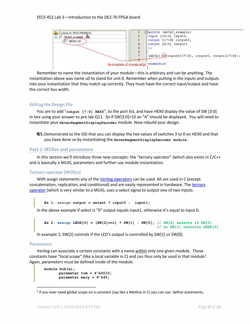
Part 1: Switch Controlled LEDs and instantiating modules. Start up Quartus by clicking on the desktop icon. Open the example
project for part 1, “File” “Open Project.” Navigate to folder lab3p1 from the files you should have downloaded from the course website. Select the file “lab3p1.qpf” and click the open button. Click lab3p1 as shown to the right. This will open up the Verilog design file. Read it over and try to understand what is happening. [17:0] SW are the 18 switches on the board, LEDR are the red LEDs and LEDG are the green LEDs.
Running Program
• Click on the toolbar to build your design. This will take about two minutes
• Go to tools in menu bar and click “In-System Memory Content Editor”.
o Select USB-Blaster for hardware o Click and open lab3p1.sof o Click to load program into FPGA
Verify that the LEDs change as you would expect them to when the switches are moved.
Instantiating modules In C you break down a design into functions. In Verilog
you break the design into modules. While they are used for similar things (breaking down a design into more manageable chunks) they are really quite different. A module is best thought of as a cookie cutter—once you’ve designed the cookie cutter you can stamp out multiple cookies. In the same way, when you create a module you can then instantiate multiple versions of the same hardware.
The basic format when instantiating a module is
o Name of module, name of instantiation, what you are inputting and outputting form the module
Version V14.2, 9/28/2014 9:14 PM Page 7 of 16
EECS 452 Lab 3—Introduction to the DE2-70 FPGA board
Remember to name the instantiation of your module—this is arbitrary and can be anything. The
instantiation above was name u0 to stand for unit 0. Remember when putting in the inputs and outputs into your instantiation that they match up correctly. They must have the correct input/output and have the correct bus width.
Editing the Design File You are to add ”output [7:0] HEX0”, to the port list, and have HEX0 display the value of SW [3:0]
in hex using your answer to pre-lab Q11. So if SW[3:0]=10 an “A” should be displayed. You will need to instantiate your SevenSegmentDisplayDecoder module. Now rebuild your design.
G1. Demonstrate to the GSI that you can display the hex values of switches 3 to 0 on HEX0 and that you have done so by instantiating the SevenSegmentDisplayDecoder module.
Part 2: MUXes and parameters In this section we’ll introduce three new concepts: the “ternary operator” (which also exists in C/C++
and is basically a MUX), parameters and further use module instantiation.
Ternary operator (MUXes) With assign statements any of the Verilog operators can be used. All are used in C (except
concatenation, replication, and conditional) and are easily represented in hardware. The ternary operator (which is very similar to a MUX), uses a select signal to output one of two inputs.
Ex 1: assign output = select ? input0 : input1;
In the above example if select is “0” output equals input1, otherwise it’s equal to input 0.
Ex 2: assign LEDR[0] = (SW[2]==1) ? SW[1] : SW[0]; // SW[2] selects if SW[0] // or SW[1] controls LEDR[0]
In example 2, SW[2] controls if the LED’s output is controlled by SW[1] or SW[0].
Parameters Verilog can associate a certain constants with a name within only one given module. These
constants have “local scope” (like a local variable in C) and can thus only be used in that module2. Again, parameters must be defined inside of the module.
module bob(a); parameter tom = 4’b0010; parameter mary = 8’h45;
2 If you ever need global scope on a constant (say like a #define in C) you can use `define statements.
Version V14.2, 9/28/2014 9:14 PM Page 8 of 16
EECS 452 Lab 3—Introduction to the DE2-70 FPGA board
Above, tom and mary are defined as constants (one 4 bit, the other 8 bit). Tom and Mary can be used in place of those constants, though only within the module bob.
Example Examine the code below. You’ll see that we are implementing the hex display differently. There are
a few differences.
1. Most trivially you’ll notice that we are sending 8 bits to the HEX0 output. The 8th bit controls the decimal point and we are turning it off.
2. We are using parameters (n0, n1, etc.) rather than directly using constants. 3. We are using nested ternary statements rather than a case statement.
lab3p2.v: module lab3p2 (SW[17:0], HEX0); input [17:0] SW; output [7:0] HEX0; bin_2_hex inst0(SW[3:0], HEX0); endmodule module bin_2_hex(bin, hex); parameter n0 = 8'b11000000; parameter n1 = 8'b11111001; parameter n2 = 8'b10100100; parameter n3 = 8'b10110000; parameter n4 = 8'b10011001; parameter n5 = 8'b10010010; parameter n6 = 8'b10000010; //Fill in the missing ones here parameter ne = 8'b10000110; parameter nf = 8'b10001110; input [3:0] bin; output [7:0] hex; assign hex = (bin == 4'h0) ? n0: (bin == 4'h1) ? n1: (bin == 4'h2) ? n2: (bin == 4'h3) ? n3: (bin == 4'h4) ? n4: (bin == 4'h5) ? n5: (bin == 4'h6) ? n6: //Fill in the missing ones here. (bin == 4'he) ? ne: nf; endmodule
Now fill in the blanks and modify the code so that the value of SW[7:4] is displayed on HEX1 and the value of SW[11:8] is displayed on HEX2.
G2. Verify that your module works with the above changes and demonstrate it to your GSI.
Part 3: Creating your own module from scratch In this part the only new thing you will do is create your own Quartus project rather than
downloading one already configured for you. We will also take a bit more advantage of being able to instantiate a module multiple times.
Version V14.2, 9/28/2014 9:14 PM Page 9 of 16

EECS 452 Lab 3—Introduction to the DE2-70 FPGA board
To create your own project, you will need to create your own design file as well as your own qsf (Quartus settings file). The qsf file matches your Verilog names (LEDR, HEX0, etc) to the physical pins on the FPGA. Your project will use multiple instantiations of the bin_2_hex module to display an 18-bit number coming from the switches on 5 of the hex displays.
Creating Your Project
• Click on “File” “New Project Wizard”
• Change the working directory to lab3/lab3p3. It will automatically create a lab3p3 folder for you.
• Set the name of the project to lab3p3. • Click “Next”, skip “Add Files” page and click “Next” again • Select “Cyclone II” in the “Family” drop down menu • In available devices select EP2C70F896C6; it is the fourth
from the bottom. • Click “Finish”
Creating a New Verilog Design File
• Once in Quartus you need to create a new design file • Click on “File” in the menu bar • Select “New” at the top of the pull down menu • Select Verilog HDL as shown to the right.
Writing the Design File You can keep multiple modules in the same file or you can split
them out. In general it’s a good idea to split them into different files if either A) the modules are likely to be needed in different projects or B) the modules are so long they will get in the way. In this part, we are going to have two modules (lab3p3 and bin_2_hex) that we will keep in two file (lab3p3.v and bin_2_hex.v). This is mainly to show that we can do it that way. Because bin_2_hex is so likely to be useful for other applications, it also makes sense to do this.
The module lab3p3, will take in all 18 switches as input and it will output a corresponding
hexadecimal number on as many hex displays as needed. You will use the bin_2_hex module for this. Since the bin_2_hex module takes in 4 inputs per 1 hex display you will instantiate it multiple times.
1. You will need to create a new module in the design file.
a. The interface will be similar to the part1 module…
module lab3p1( input [17:0] SW, //switches on FPGA output [17:0] LEDR, //red leds on FPGA //add the HEX0 display here output [7:0] LEDG //green leds on FPGA );
b. The module name is to be lab3p3 and the file name is to be lab3p3.v.
Version V14.2, 9/28/2014 9:14 PM Page 10 of 16

EECS 452 Lab 3—Introduction to the DE2-70 FPGA board
c. The inputs will be all 18 switches d. The outputs will be HEX0, HEX1, etc. There are eight hex displays total, but only use
what you need. 2. Create the file bin_2_hex.v and then copy the bin_2_hex module into it. 3. Instantiate the bin_2_hex module in the lab3p3.v file (as many times as needed to do the
job). This should be done outside of any other module. 4. Include “endmodule”. Your design file is complete.
Modifying the QSF File The QSF file tells the tools the physical pin that is associated with your Verilog input/output name. You will need to save the project before you modify the QSF file.
• Go to “File” • Select “Open” • Change the files of type to: All
Files(*.*) • Select lab3p3.qsf • You will need to copy and paste the
pin assignments you need from default.qsf (in the FPGA Support Files found on the course website.) You can just copy and paste the whole file if you choose, however this will result in a quite a few warnings. Instead you can copy only those wires you’ll be using.
• Make sure you have the following line in your .qsf from default.qsf set_global_assignment -name CYCLONEII_RESERVE_NCEO_AFTER_CONFIGURATION "USE AS REGULAR IO"
• Save the qsf file (otherwise the next step won’t quite do what you want).
Including Design Files You will need to tell the tools what design files you are using.
• Go back “Assignments” in the menu bar • Select “Settings” and click “Files” from “Category” on the left hand side • You have to include the design files that you want to use for your project
• Add the design file lab3p3.v and design file bin_2_hex.v
Version V14.2, 9/28/2014 9:14 PM Page 11 of 16

EECS 452 Lab 3—Introduction to the DE2-70 FPGA board
You are ready to build and run your code.
G3. Verify that your module works. Your GSI will check not only for functionality but that you have two different .v files and that you’ve set up the qsf file correctly.
Part 4: Sequential Logic Part 1 Design a D flip-flop that uses KEY[3] as the clock, switch 0 as the D input and green LED 0 as the
output.
Note: the KEYs on the FPGA board are active low and debounced whereas the switches are not. So you may want to use the KEYs as a clock signal but not the switches.
G4. Demonstrate your flip-flop to your GSI.
Part 5: Sequential Logic Part 2 Get the state machine code (lab3p5.v) in pre-lab problem Q10 working on the board. Remember
that the keys are active low. Use KEY[3] as the clock, KEY[2] as reset and switch 0 as the input. Use some of the red LEDs to display the output.
Q1. What output do you get if, after reset, you input a “1010”?
G5. Demonstrate this state machine to your GSI. Show the behavior of the input “11100”.
Section B: Generating a signal Now we are going to use Direct Digital Synthesis to generate sine waves, just as we did in labs 1 and
2. In this section we will work with two slightly different modules. The first will take the generated waveform and output it on the “line out” audio jack on the FPGA board. The second will take the generated waveform and display it on the VGA display. In both cases, you are supplied with code that uses a 16-entry sine table.
Part 6: Audio DDS Open the Verilog project associated with this part, top.qpf in lab3p6 folder. It consists of five
Verilog files (much of which is dedicated sending the waveform out the line out jack). Connect the Altera board’s LINE_OUT jack to the Oscilloscope. Build and run the project. Be aware that some of the switches control the exact frequency. Be sure to look over the ‘AUDIO.v’ code for the questions.
Q2. Observe the output when only SW0 is a “1”.
a. Measure the frequency of the waveform it generates. b. Is there anything odd or unexpected about the waveform?
Q3. Now look over the code. a. What is the value of FTV for the situation you observed in Q2? b. What is the sampling rate? c. Compute the expected frequency for the case you observed in Q2. Show your work.
Modify the code so that the table has 64 entries and the register is 16 bits instead of 10 (you should
also increase the range of FTV values by a similar amount so you can still generate high-frequency
Version V14.2, 9/28/2014 9:14 PM Page 12 of 16

EECS 452 Lab 3—Introduction to the DE2-70 FPGA board
signals. You’ll do this by using more switches). You may find the MATLAB code on page 5 of pre-lab useful.
Q4. What is the lowest frequency signal you can now generate? The highest?
G6. Demonstrate your DDS code with a 64-entry table to your GSI.
Part 7: Audio DDS with MegaFunctions and Linear Interpolation Many student projects involve nontrivial memory requirements, and the DE2-70 provides many
memory units with large storage capacities. This simple exercise will introduce you to memory megafunctions, which are modules you can instantiate that give you access to memory units. Specifically, we will use the ROM: 2-Port megafunction to store our DDS sine wave values.
Start by using the Quartus project you used for the previous section. Create a new Verilog module called ‘DDSRAM’ and use the same input and output wires as the DDS module. Next, go to Tools -> MegaWizard Plug-in Manager to launch the GUI where you can design all of your megafunctions. Select ‘Create a new custom megafunction variation’ and click ‘Next’. You will see the following interface with all available megafunctions.
On the left hand side expand the ‘Memory Compiler’ section and selection the ROM: 2-PORT option.
Be sure to select ‘Verilog HDL’ option. You can name the output file anything you want (we called ours sineRom.) Click “Next.” It might take a few seconds but shortly you should see the ROM: 2-PORT wizard. You will see a block diagram on the left hand side that shows the IO to the module. For this example, set the width of the ‘q_a’ bus to 16 bits and set 64 words in memory. Choose the M4K memory block type. Click “Next”, leave everything as default for the ‘Clks/Rd, Byte En’ and ‘Regs/Clkens/Aclrs’ steps.
In the ‘Mem Init’ panel, click ‘Yes, use this file for memory content data’. Browse to sintable.mif. It is located in lab3_Files.zip. Click ‘Next’ and skip the EDA step. In the summary panel make sure to also generate the instantiation template file. Click ‘Finish’ and if you see an alert about IP, you can click either option. After you’ve built your first megafunction, you need to instantiate it inside your DDSRAM
Version V14.2, 9/28/2014 9:14 PM Page 13 of 16

EECS 452 Lab 3—Introduction to the DE2-70 FPGA board
module. In your workspace you should see that Quartus has created numerous files for you. Find the one that is your instantiation file. It should be named ‘x_inst.v’ where ‘x’ is what you called your megafunction. Inside this file you’ll find the template for instantiation. Copy it over to your DDS module.
You’ll notice that the megafunction uses five ports: 2 addresses, a clock, and 2 outputs. For now we will only use one address-output pair, so assign the output of the DDS module to be the output from one of the q ports. Remember that you still need to use counter to index your table.
G7. Demonstrate your DDS using a megafunction working to the GSI.
Although this exercise was very contrived, it’s easy to see that for very large (think KBs or MBs
required for handling audio storage or video storage) memory megafunctions would be extremely useful. In addition, megafunctions provide optimized implementations for a variety of other functionalities.
Open up Code Composer Studio and launch into the Debug perspective (You can use a previous CCS
project, or create a dummy one). Once in the Debug perspective, do not ‘Start’ the CCS program you launched the Debugger with. Instead, click on the ‘Run’ tab at the top, navigate to ‘Load’, and click ‘Load Program’. Browse to find the SpectrumAnalysis.out program from Lab3_files. Run the program and you will see a prompt. Use 4 scans to incoherently sum, with Chebyshev windowing. Plug the audio out on the DE2-70 to the Stereo In of the C5515. Now plug in the C5515 to your computer via the UART breakout board and miniUSB to USB cable and launch the WindowPlot.exe program (Make sure the dll file is in the same directory as WIndowPlot.exe). When prompted by the WindowsPlot.exe program, hit ‘y’ for double buffering. After a few seconds you should see the plot. Tune your DDS so that the output frequency is at 750 Hz. Save this to an image.
Now download the DDRAM2.sv file from Ctools, add it to your Quartus project, and instantiate the
module in ‘top’. Use one of the switches to toggle between the output of your DDSRAM and the ‘iDataOut’ output of this DDRAM2 with linear interpolation. Save the spectra from DDS with linear interpolation.
Q5. What’s the biggest difference between the two spectra you see? Your answer should discuss a
certain kind of noise.
Part 8: VGA displayed DDS Now open the Verilog project associated with this part. Connect the VGA output of the FPGA board
to the VGA input on one of your monitors. Build and run the project. Change the monitor setting so that it is displaying the VGA output. Once again, the switches on the FPGA board control the FTV value. Play with the code for a bit.
Q6. Observe the output when only SW2 is a “1”. About how many periods do you observe?
Signed numbers and multiplication For addition, the signed and unsigned results are the same (from a bitwise perspective) but this is
not true for multiplication and so Verilog needs to know if you want signed or unsigned multiplication. If you are multiplying two numbers and you want to be doing signed multiplication, both operands must be signed. You can make constants signed by adding an “s” to the representation type. For example, 5’sb10000 is a signed number. You can make wires or regs signed by adding the signed keyword as we
Version V14.2, 9/28/2014 9:14 PM Page 14 of 16

EECS 452 Lab 3—Introduction to the DE2-70 FPGA board
did in the FIR filter. If you use bit selection or something else as a number, it will be treated as unsigned and that can cause problems. The easiest way to deal with this is to put the bits selected into a temporary variable. So rather than assign bob=bob[3:1]*2’sd3 (which will cause unsigned multiplication) try the following (assuming bob and tmp are declared as signed values).
assign tmp=bob[3:1]; assign bob=tmp*2’sd3;
There are numerous other things you can do, including the equivalent of casting3. Q7. Now look over the code.
a. Notice we are using the same DDS as in the audio part however the range of the values outputted to the VGA is completely different (it’s now from 40 to 450 vs. -32768 to 32767 in the audio case). Find the code that does this conversion and explain what’s going on.
b. Notice that VGA_R, VGA_B and VGA_G are all 10 bits but only take the values 0 and -1. What color do you suppose is associated with each of those two?
Modify the DDS module so that you have a 64-entry table that uses the same output range as the
current 16-entry table. The Matlab code found in the pre-lab might again be useful. Also change the output so the plotted points are blue and the background is yellow.
G8. Demonstrate your modified project to the GSI.
Part 9: Using multiple instances of DDS to generate specific outputs Your task is to generate two periods of a sawtooth wave on the VGA display. The MATLAB code you
worked on in the pre-lab is a good starting point. In addition, you will want to draw two periods of sine wave on the display first to verify your choice of FTV and the code that does the scaling before working on the sawthooth.
Note: you should not use the switches to find the FTV value; instead you should use the MATLAB code from pre-lab. Also you are not supposed to use division or floating-point numbers in Verilog. Calculation involving dividing or floating point should be done outside FPGA.
G9. Demonstrate the two periods of a sine wave that is scaled by 1 over pi on the VGA display to
your GSI. Now work on generating the sawtooth on the VGA display. Here you need to instantiate multiple
DDS instances to generate different harmonics in the Fourier series. Again, the Matlab code from pre-lab will be very useful. Do not forget about Fourier coefficients and that signed decimal numbers should be denoted as ‘sd’ in Verilog. Finally, one simple way to do ‘bit-shifting’ in Verilog is to select those bits you want.
G10. Demonstrate your sawtooth to your GSI.
3 See http://www.uccs.edu/~gtumbush/published_papers/Tumbush%20DVCon%2005.pdf for a really nice overview on this topic.
Version V14.2, 9/28/2014 9:14 PM Page 15 of 16

EECS 452 Lab 3—Introduction to the DE2-70 FPGA board
Q8. Print out your code for the sawtooth and turn it in with your other questions.
You will want to look over the post-lab before leaving…
4. Post-lab For some of these questions you will want to observe the output carefully so you’ll at least need to
start some of these questions in lab… Q9. You likely noticed that the waveform generated by the table had some unusual characteristics
when put on the oscilloscope. Think about the FPGA hardware. a. At lower frequencies the corners were not overly sharp. b. At higher frequencies the amplitude was attenuated. c. In some cases the output appears to saturate.
Why do you think these effects are occurring? (Note: there may be different reasons for each and perhaps multiple reasons for some. This is a tricky question.)
Q10. Read a bit about VGA (http://www.nathandumont.com/node/241 and perhaps http://www.eecg.toronto.edu/~tm4/rgbout.html may be useful).
a. What is a “porch” in this context? b. Explain why this version of the DDS module has “lineend”. c. Looking at the code form Q7, explain why the output doesn’t seem to start at the
beginning of the sine wave.
Version V14.2, 9/28/2014 9:14 PM Page 16 of 16