eecs 150 -- digital designcs150/sp10/lecture/lec04-sds-review2.pdf · eecs 150 - l4: synch systems...
TRANSCRIPT

UC Regents Spr 2010 © UCBEECS 150 - L4: Synch Systems II
2010-1-28John Wawrzynek
EECS 150 -- Digital Design
Lecture 4 – Synchronous Digital Systems Review (Part II)
www-inst.eecs.berkeley.edu/~cs150
Today’s lecture by John Lazzaro
1Thursday, January 28, 2010
Spring 2010 EECS150 lec04-SDS-review2 Page
EECS150 - Digital DesignLecture 4 - Synchronous
Digital Systems Review Part 2January 28, 2010
John WawrzynekElectrical Engineering and Computer Sciences
University of California, Berkeley
http://www-inst.eecs.berkeley.edu/~cs150
2
2Thursday, January 28, 2010

Spring 2010 EECS150 lec04-SDS-review2 Page
Outline• Topics in the review, you have already seen in
CS61C, and possibly EE40:1. Digital Signals.2. General model for synchronous systems.3. Combinational logic circuits 4. Flip-flops, clocking
3
3Thursday, January 28, 2010

UC Regents Spr 2010 © UCBEECS 150 - L4: Synch Systems II
Today’s Lecture
Flip-flop-based state machines
Registers and Pipelining
Register-based state machines
Flip-flop details ...
Operates on Boolean (single-bit) values.
Operates on multi-bit values (integers, CPU instruction, ...)
Adding state to speed up the clock.
(Reset, set, etc ...)
4Thursday, January 28, 2010
UC Regents Spr 2010 © UCBEECS 150 - L4: Synch Systems II
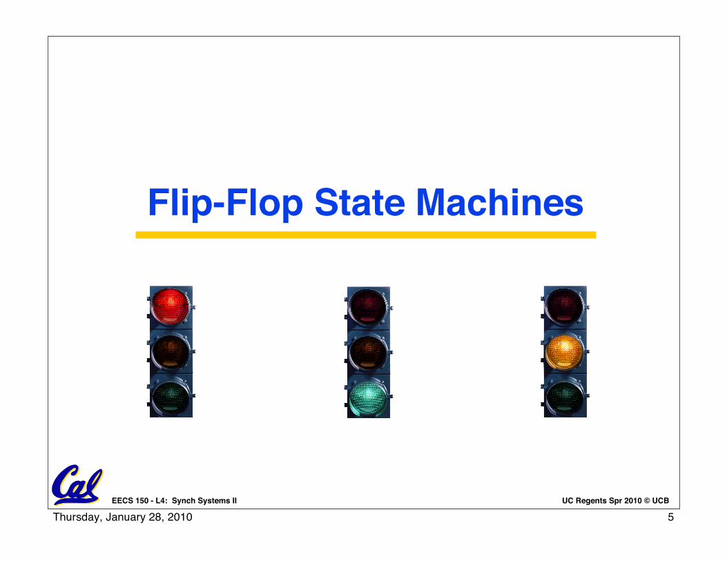
Flip-Flop State Machines
5Thursday, January 28, 2010

UC Regents Spr 2010 © UCBEECS 150 - L4: Synch Systems II
A Simple System: Traffic Light Controller
R Y G1 0 0
R Y G0 0 1
R Y G0 1 0
Power up to red
state
Show each light for 1 second.
“Loop” forever.
6Thursday, January 28, 2010
UC Regents Spr 2010 © UCBEECS 150 - L4: Synch Systems II
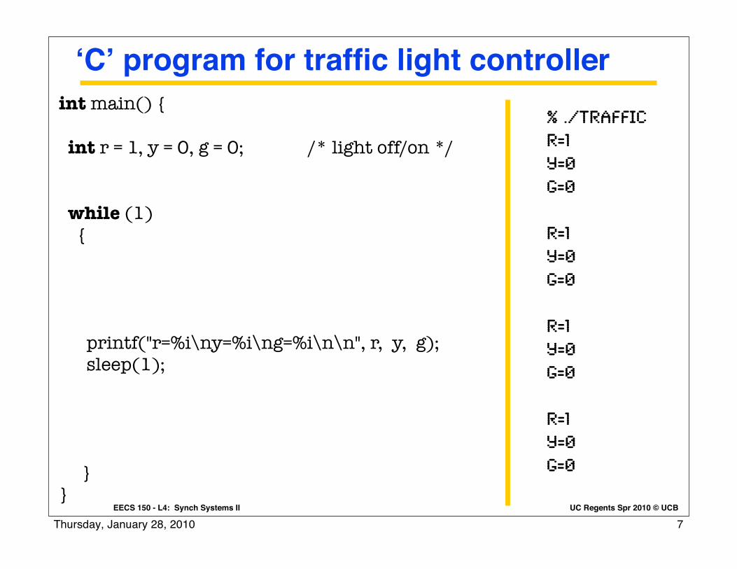
‘C’ program for traffic light controllerint main() {
int r = 1, y = 0, g = 0; /* light off/on */
while (1) {
printf("r=%i\ny=%i\ng=%i\n\n", r, y, g); sleep(1);
}}
% ./trafficr=1y=0g=0
r=1y=0g=0
r=1y=0g=0
r=1y=0g=0
7Thursday, January 28, 2010

UC Regents Spr 2010 © UCBEECS 150 - L4: Synch Systems II
‘C’ program for traffic light controllerint main() {
int r = 1, y = 0, g = 0; /* light off/on */
while (1) {
printf("r=%i\ny=%i\ng=%i\n\n", r, y, g); sleep(1);
}}
int next_r, next_y, next_g; /* extra state */
next_r = y; next_y = g; next_g = r;
r = next_r; y = next_y; g = next_g;
% ./trafficr=1y=0g=0
r=0y=0g=1
r=0y=1g=0
r=1y=0g=0
r=0y=0g=1
Compute the “next” state for the traffic light.
Make the “next” state the “current” state of the traffic light.
8Thursday, January 28, 2010
UC Regents Spr 2010 © UCBEECS 150 - L4: Synch Systems II
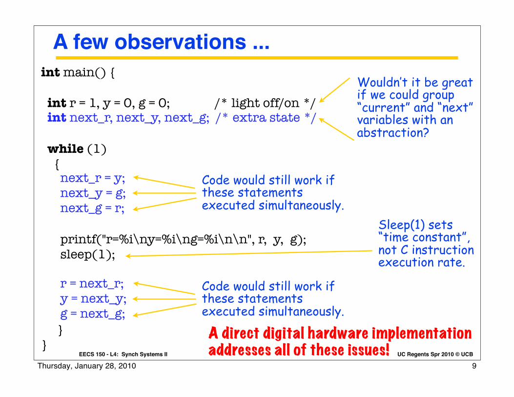
int main() {
int r = 1, y = 0, g = 0; /* light off/on */
while (1) {
printf("r=%i\ny=%i\ng=%i\n\n", r, y, g); sleep(1);
}}
int next_r, next_y, next_g; /* extra state */
next_r = y; next_y = g; next_g = r;
r = next_r; y = next_y; g = next_g;
A few observations ...
Code would still work if these statements executed simultaneously.
Code would still work if these statements executed simultaneously.
Wouldn’t it be great if we could group “current” and “next” variables with an abstraction?
Sleep(1) sets “time constant”, not C instruction execution rate.
A direct digital hardware implementation addresses all of these issues!
9Thursday, January 28, 2010

UC Regents Spr 2010 © UCBEECS 150 - L4: Synch Systems II
Clock waveform takes the role of sleep(1)
!"#$%&'())* ++,!-.)'/ 012-)34$5$%& 67&1'8
!"#$%&'
( )#*#&&'&+,-+.'*/#&+0-12'*,'*3+
#
4 5+! ,/$'60&7"89+:+,/$'6$;"9+:+,/$'6.',;%9
5+! #0&7"8 :+#$;" :+#.',;%
0&7
f T
1 Hz 1 s
1 MHz 1 μs
1 GHz 1 ns
All state changes happen on leading edge of our 1 Hz clock ... thus, lights will switch once per second.
1 second (posedge to posedge)
10Thursday, January 28, 2010

UC Regents Spr 2010 © UCBEECS 150 - L4: Synch Systems II
r & next_r? One edge-triggered D flip-flop
D Q
CLK
Value of D is sampled on positive clock edge.
Q outputs sampled value for rest of cycle.
D
Q
Positive-edge sampling makes it easy to think about state.
11Thursday, January 28, 2010

Spring 2010 EECS150 lec04-SDS-review2 Page
Flip-flop Timing Waveforms?• Edge-triggered d-type flip-flop
– This one is “positive edge-triggered”• “On the rising edge of the clock, the input d is
sampled and transferred to the output. At all other times, the input d is ignored.”
• Example waveforms:
12
12Thursday, January 28, 2010
UC Regents Spr 2010 © UCBEECS 150 - L4: Synch Systems II
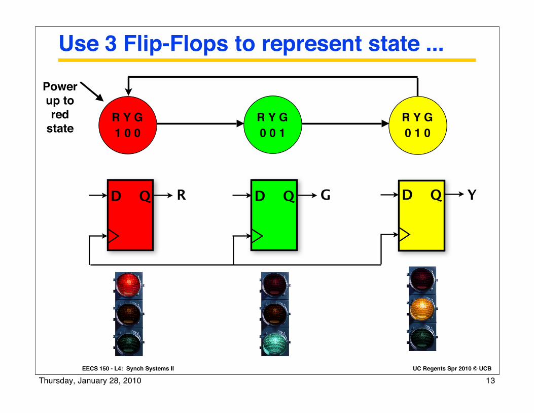
Use 3 Flip-Flops to represent state ...
D QD Q D QR G Y
R Y G1 0 0
R Y G0 0 1
R Y G0 1 0
Power up to red
state
13Thursday, January 28, 2010

UC Regents Spr 2010 © UCBEECS 150 - L4: Synch Systems II
Use 3 Flip-Flops to represent state ...
D QD Q D QR G Y
“One-Hot Encoding”: State machines where exactly one D flip-flop is in the “1” state at a time (forbidden states: RYG = 000, 011, 101, 110, 111).
R Y G1 0 0
R Y G0 0 1
R Y G0 1 0
Power up to red
state
14Thursday, January 28, 2010

UC Regents Spr 2010 © UCBEECS 150 - L4: Synch Systems II
“Simplified” traffic light controller
R Y G1 0 0
R Y G0 0 1
R Y G0 1 0
Power up to red
state
Next State Combinational Logic
D QD Q D QR G Y
“Simplified???”: We assume the state at the beginning of time is RYG == 100. A “complete” implementation would include “power up” logic.
15Thursday, January 28, 2010

UC Regents Spr 2010 © UCBEECS 150 - L4: Synch Systems II
Inside the combinational logic box ...
R Y G1 0 0
R Y G0 0 1
R Y G0 1 0
Power up to red
state
Next State Combinational Logic
D QD Q D QR G Y
Let’s revisit our original C code ...16Thursday, January 28, 2010

UC Regents Spr 2010 © UCBEECS 150 - L4: Synch Systems II
int main() {
int r = 1, y = 0, g = 0; /* light off/on */
while (1) {
printf("r=%i\ny=%i\ng=%i\n\n", r, y, g); sleep(1);
}}
int next_r, next_y, next_g; /* extra state */
next_r = y; next_y = g; next_g = r;
r = next_r; y = next_y; g = next_g;
Recall: A few observations ...
6 C variables, but only 3 flip-flops. How does that work?
17Thursday, January 28, 2010

UC Regents Spr 2010 © UCBEECS 150 - L4: Synch Systems II
Flip-flops have an internal output delay ...
D Q
CLK
D
Qt_clk-to-Q
Value of D is sampled on positive clock edge.
Q changes t_clk_to_Q seconds after the positive edge happens (t_clk_to_Q > 0).
18Thursday, January 28, 2010

UC Regents Spr 2010 © UCBEECS 150 - L4: Synch Systems II
And so, even this circuit “works” ...
CLK
D
Qt_clk-to-Q
D Q
CLK
Value of D is sampled on positive clock edge.
t_inv = 0
Assume inverter has no delay ! (real-world inverters always have delay).
Flip-flip t_clk_to_Q delay is positive.
Circuit “goal”: 0->1->0->1-> ... toggle on posedge.
t_clk-to-Q
Q can’t “race” back to D in time to “catch” the positive edge that caused it ... and so the “next” variables are not needed!
19Thursday, January 28, 2010

UC Regents Spr 2010 © UCBEECS 150 - L4: Synch Systems II
int main() {
int r = 1, y = 0, g = 0; /* light off/on */
while (1) {
printf("r=%i\ny=%i\ng=%i\n\n", r, y, g); sleep(1);
}}
int next_r, next_y, next_g; /* extra state */
next_r = y; next_y = g; next_g = r;
r = next_r; y = next_y; g = next_g;
Recall: A few observations ...
Where does this show up in the circuit??
Where does this show up in the circuit?
20Thursday, January 28, 2010

Next State Combinational Logic
D QD Q D QR G Y
Dr
Qr
Dg
Qg
Dy
Qy
CLK
From yellow to red...
0
0
1
0
0
1
0
0
1
0
1
0
t_clk-to-Q
logic delay
From redto green on next clock edge.
0
1
0
21Thursday, January 28, 2010
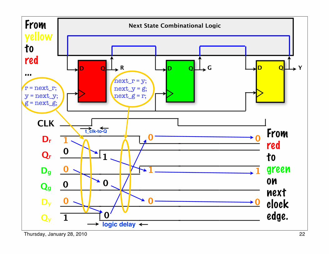
Next State Combinational Logic
D QD Q D QR G Y
Dr
Qr
Dg
Qg
Dy
Qy
CLK
From yellow to red...
0
0
1 0
0
10
0
1 0
1
0
t_clk-to-Q
logic delay
From redto green on next clock edge.
0
1
0
r = next_r;y = next_y;g = next_g;
next_r = y;next_y = g;next_g = r;
22Thursday, January 28, 2010

UC Regents Spr 2010 © UCBEECS 150 - L4: Synch Systems II
How fast can we run the clock?
Next State Combinational Logic
D QD Q D QR G Y!"#$%&'())* ++,!-.)'/ 012-)34$5$%& 67&1'8
!"#$%&'
( )#*#&&'&+,-+.'*/#&+0-12'*,'*3+
#
4 5+! ,/$'60&7"89+:+,/$'6$;"9+:+,/$'6.',;%9
5+! #0&7"8 :+#$;" :+#.',;%
0&7
Timing AnalysisWhat is the
smallest T that produces correct
operation?An entire lecture (later in semester), here is the short version ...
23Thursday, January 28, 2010

UC Regents Spr 2010 © UCBEECS 150 - L4: Synch Systems II
D must stablize ahead of positive edge
D Q
CLK
Value of D is sampled on positive clock edge.
Q changes t_clk_to_Q seconds after the positive edge happens.
D
Q
t_setup
t_clk-to-Q
D must be a stable “0” or “1” by t_setup seconds before the positive edge happens.
24Thursday, January 28, 2010

UC Regents Spr 2010 © UCBEECS 150 - L4: Synch Systems II
Revisiting the toggle circuit ...
D Q
CLK
Value of D is sampled on positive clock edge.Flip-flip t_clk_to_Q delay is positive.
Circuit “goal”: 0->1->0->1-> ... toggle on posedge.t_inv > 0
Inverter t_inv delay is positive.t_setup
t_inv delay must fit in
this time slot!
T: the clock period
CLK
D
Q 0
1
t_clk-to-Q
0
1 0
1
T > t_clk_to_Q + t_inv + t_setup
25Thursday, January 28, 2010

UC Regents Spr 2010 © UCBEECS 150 - L4: Synch Systems II
Or, more generally ...
!"#$%&'())* ++,!-.)'/ 012-)34$5$%& 67&1'8
!"#$%&'
( )#*#&&'&+,-+.'*/#&+0-12'*,'*3+
#
4 5+! ,/$'60&7"89+:+,/$'6$;"9+:+,/$'6.',;%9
5+! #0&7"8 :+#$;" :+#.',;%
0&7
Combinational Logic (CL) “time budget”
!"#$%&'())* ++,!-.)'/ 012-)34$5$%& 67&1'8
!"#"$%&'()*"&')+',-#./$)#)01'23$.034
5 6#'7"#"$%&8'+)$'.)$$".4')9"$%43)#:
+)$'%&&'9%4/1;
5 <)='*)'="'"#0>"$%4"'!""#$!%&'?
@ A#-'.3$.034'3#904')$'$"7314"$')04904'4)'%#-'$"7314"$'3#904')$'.3$.034'
)04904;
@ B1"409'43>"C'+)$'.3$.034')049041'*"9"#*1')#'=/%4'34'.)##".41'4)
@ B.&DEF'43>"C'+)$'.3$.034'3#9041'*"9"#*1')#'+$)>'=/"$"'34'.)>"1;
$"7 $"72G 2G
.&).D 3#904
)04904
)943)#'+""*H%.D
3#904 )04904
I'! 43>"J.&D"FK'L'43>"J2GK'L'43>"J1"409K
I'! #.&D"F L'#2G L'#1"409
1/28/04 ©UCB Spring 2004CS152 / Kubiatowicz
Lec3.9
General C/L Cell Delay Model
° Combinational Cell (symbol) is fully specified by:• functional (input -> output) behavior
- truth-table, logic equation, VHDL
• Input load factor of each input
• Propagation delay from each input to each output for each transition
- THL(A, o) = Fixed Internal Delay + Load-dependent-delay x load
° Linear model composes
Cout
Vout
Cout
Delay
Va -> Vout
XX
X
X
X
X
Ccritical
delay per unit load
A
B
X
.
.
.
Combinational
Logic Cell
Internal Delay
1/28/04 ©UCB Spring 2004CS152 / Kubiatowicz
Lec3.10
Storage Element’s Timing Model
Clk
D Q
° Setup Time: Input must be stable BEFORE trigger clock edge
° Hold Time: Input must REMAIN stable after trigger clock edge
° Clock-to-Q time:
• Output cannot change instantaneously at the trigger clock edge
• Similar to delay in logic gates, two components:
- Internal Clock-to-Q
- Load dependent Clock-to-Q
Don’t Care Don’t Care
HoldSetup
D
Unknown
Clock-to-Q
Q
1/28/04 ©UCB Spring 2004CS152 / Kubiatowicz
Lec3.11
Clocking Methodology
Clk
Combination Logic.
.
.
.
.
.
.
.
.
.
.
.
° All storage elements are clocked by the same clock edge
° The combination logic blocks:• Inputs are updated at each clock tick
• All outputs MUST be stable before the next clock tick
1/28/04 ©UCB Spring 2004CS152 / Kubiatowicz
Lec3.12
Critical Path & Cycle Time
Clk
.
.
.
.
.
.
.
.
.
.
.
.
° Critical path: the slowest path between any two storage devices
° Cycle time is a function of the critical path
° must be greater than:
Clock-to-Q + Longest Path through Combination Logic + Setup
Combinational Logic
One part of a long story, to be told later in semester ...26Thursday, January 28, 2010

UC Regents Spr 2010 © UCBEECS 150 - L4: Synch Systems II
Some Flip Flops have “hold” time ...
D
t_setup
CLK
t_hold
D must stay
stable here
D Q
CLK
If t_hold > 0, this circuit may fail even if t_inv > 0 and t_clk_to_Q > 0 !!!
t_inv
t_clk-to-Q + t_inv > t_holdFor correct operation.
27Thursday, January 28, 2010

Spring 2010 EECS150 lec04-SDS-review2 Page
Flip-Flop Timing Details
Three important times associated with flip-flops:setup timehold timeclock-to-q delay.
28
FF
clk
d q
28Thursday, January 28, 2010
UC Regents Spr 2010 © UCBEECS 150 - L4: Synch Systems II
Register State Machines
29Thursday, January 28, 2010

UC Regents Spr 2010 © UCBEECS 150 - L4: Synch Systems II
Register: Holds an ordered set of bits
Sometimes, we will add an “enable” input: clock edge updates state only if enable is high.
32Din
Clk
PC
Dout32
Built out of an array of flip-flops
D Q
clk
D Q
D Q
Din0
Din1
Din2
Dout0
Dout1
Dout2
30Thursday, January 28, 2010

Spring 2010 EECS150 lec04-SDS-review2 Page
State Elements: circuits that store info
• The value stored by the register appears on the output (after a small delay).
• Until the next load, changes on the data input are ignored (unlike CL, where input changes change output).
• These get used for short term storage (ex: register file), and to help move data around the processor.
Examples: registers, memories
Register: Under the control of the “load” signal, the register captures the input value and stores it indefinitely.
register
output
input
load
n
n
often replace by clock signal (clk)
31
31Thursday, January 28, 2010
Spring 2010 EECS150 lec04-SDS-review2 Page
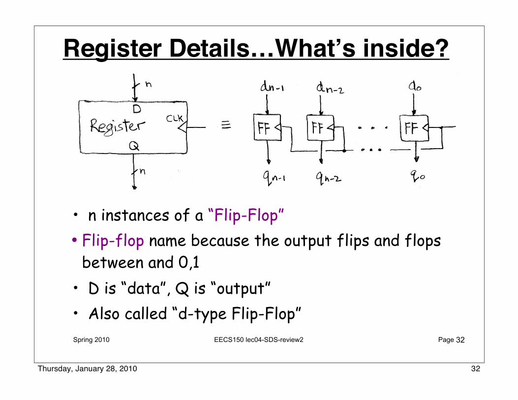
Register Details…What’s inside?
• n instances of a “Flip-Flop”• Flip-flop name because the output flips and flops
between and 0,1 • D is “data”, Q is “output”• Also called “d-type Flip-Flop”
32
32Thursday, January 28, 2010

UC Regents Spr 2010 © UCBEECS 150 - L4: Synch Systems II
Multi-bit adder: Doing logic on an integer
Combinational: Put a A and B values on inputs, a short time later A + B appears on output.
32+
32
32
A
B
A + B
Just like we use gates to operate on Q output of a flip-flop, we use components like multi-bit adders to operate on all output bits of a register.
33Thursday, January 28, 2010
UC Regents Spr 2010 © UCBEECS 150 - L4: Synch Systems II
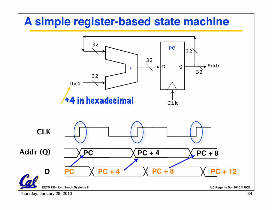
A simple register-based state machine
Clk
Addr32
D
PC
Q32
32
+
32
320x4
+4 in hexadecimal
PC + 12PC + 8PC + 4
CLK
Addr (Q)
D PC
PC PC + 4 PC + 8
34Thursday, January 28, 2010

Spring 2010 EECS150 lec04-SDS-review2 Page
Accumulator Circuit Example
• We need something like this:
Assume X is a vector of N integers, presented to the input of our accumulator circuit one at a time (one per clock cycle), so that after N clock cycles, S hold the sum of all N numbers.
S=0; Repeat N times S = S + X;
But not quite.Need to use the clock signal to hold up the feedback to match up with the input signal.
X
35
35Thursday, January 28, 2010

Spring 2010 EECS150 lec04-SDS-review2 Page
Accumulator Circuit• Put register, with clock signal
controlling its load, in feedback path.• On each clock cycle the register
prevents the new value from reaching the input to the adder prematurely. (The new value just waits at the input of the register).
36
Timing:
36Thursday, January 28, 2010

Spring 2010 EECS150 lec04-SDS-review2 Page
Register Details (again)• A n-bit wide register is nothing but a set of flip-flops (1-bit wide
registers) with a common load/clk signal.
• A flip-flop captures its input on the edge of the clock (rising edge in this case - positive edge flip-flop). The new input appears at the output after a short delay.
37
37Thursday, January 28, 2010

Spring 2010 EECS150 lec04-SDS-review2 Page
Accumulator Revisited
38
• Note:– Reset signal
(synchronous)– Timing of X signal is not
known without investigating the circuit that supplies X. Here we assume it comes just after Si-1.
– Observe transient behavior of Si.
38Thursday, January 28, 2010

Spring 2010 EECS150 lec04-SDS-review2 Page
Only Two Types of Circuits Exist• Combinational Logic Blocks (CL)• State Elements (registers)
State elements are mixed in with CL blocks to control the flow of data.
39
Register fileor
Memory Block
AddressInput Data
Output DataWrite Control
clock
Sometimes used in large groups by themselves for “long-term” data storage.
39Thursday, January 28, 2010

UC Regents Spr 2010 © UCBEECS 150 - L4: Synch Systems II
Register File example: MIPS R-format CPU
32rd1
RegFile
32rd2
WE32wd
5rs1
5rs2
5ws
32ALU
32
32
op
opcode rs rt rd functshamt
Decode fields to get : ADD $8 $9 $10
Logic
40Thursday, January 28, 2010

UC Regents Spr 2010 © UCBEECS 150 - L4: Synch Systems II
MIPS Register file: From the top down
R1
R2
...
R31
Why is R0 special?
Q
Q
Q
R0 - The constant 0 Q
clk
.
.
.
32MUX
32
32
sel(rs1)
5
.
.
.
rd1
32MUX
32
32
sel(rs2)
5
.
.
.
rd2
“two read ports”
D
D
D
En
En
En
DEMUX
.
.
.
sel(ws)5
WE
wd
32
41Thursday, January 28, 2010

Spring 2010 EECS150 lec04-SDS-review2 Page
Uses for State Elements1) As a place to store values for some indeterminate
amount of time:– Register files (like $1-$31 on the MIPS)– Memory (caches, and main memory)
2) Help control the flow of information between combinational logic blocks.
– State elements are used to hold up the movement of information at the inputs to combinational logic blocks and allow for orderly passage.
42
42Thursday, January 28, 2010
UC Regents Spr 2010 © UCBEECS 150 - L4: Synch Systems II
Pipelining and Registers
43Thursday, January 28, 2010

Spring 2010 EECS150 lec04-SDS-review2 Page
Pipelining to improve performance (1/2)
Timing…
Extra Register are often added to help speed up the clock rate.
Note: delay of 1 clock cycle from input to output.Clock period limited by propagation delay of adder/shifter.
44
44Thursday, January 28, 2010

Spring 2010 EECS150 lec04-SDS-review2 Page
Pipelining to improve performance (2/2)
Timing…
Insertion of register allows higher clock frequency.More outputs per second.
45
45Thursday, January 28, 2010

UC Regents Spr 2010 © UCBEECS 150 - L4: Synch Systems II
Pipelining in a real CPU design ...
Goal: Increase clock frequency by reducing delay between registers.
1600 IEEE JOURNAL OF SOLID-STATE CIRCUITS, VOL. 36, NO. 11, NOVEMBER 2001
Fig. 1. Process SEM cross section.
The process was raised from [1] to limit standby power.
Circuit design and architectural pipelining ensure low voltage
performance and functionality. To further limit standby current
in handheld ASSPs, a longer poly target takes advantage of the
versus dependence and source-to-body bias is used
to electrically limit transistor in standby mode. All core
nMOS and pMOS transistors utilize separate source and bulk
connections to support this. The process includes cobalt disili-
cide gates and diffusions. Low source and drain capacitance, as
well as 3-nm gate-oxide thickness, allow high performance and
low-voltage operation.
III. ARCHITECTURE
The microprocessor contains 32-kB instruction and data
caches as well as an eight-entry coalescing writeback buffer.
The instruction and data cache fill buffers have two and four
entries, respectively. The data cache supports hit-under-miss
operation and lines may be locked to allow SRAM-like oper-
ation. Thirty-two-entry fully associative translation lookaside
buffers (TLBs) that support multiple page sizes are provided
for both caches. TLB entries may also be locked. A 128-entry
branch target buffer improves branch performance a pipeline
deeper than earlier high-performance ARM designs [2], [3].
A. Pipeline Organization
To obtain high performance, the microprocessor core utilizes
a simple scalar pipeline and a high-frequency clock. In addition
to avoiding the potential power waste of a superscalar approach,
functional design and validation complexity is decreased at the
expense of circuit design effort. To avoid circuit design issues,
the pipeline partitioning balances the workload and ensures that
no one pipeline stage is tight. The main integer pipeline is seven
stages, memory operations follow an eight-stage pipeline, and
when operating in thumb mode an extra pipe stage is inserted
after the last fetch stage to convert thumb instructions into ARM
instructions. Since thumb mode instructions [11] are 16 b, two
instructions are fetched in parallel while executing thumb in-
structions. A simplified diagram of the processor pipeline is
Fig. 2. Microprocessor pipeline organization.
shown in Fig. 2, where the state boundaries are indicated by
gray. Features that allow the microarchitecture to achieve high
speed are as follows.
The shifter and ALU reside in separate stages. The ARM in-
struction set allows a shift followed by an ALU operation in a
single instruction. Previous implementations limited frequency
by having the shift and ALU in a single stage. Splitting this op-
eration reduces the critical ALU bypass path by approximately
1/3. The extra pipeline hazard introduced when an instruction is
immediately followed by one requiring that the result be shifted
is infrequent.
Decoupled Instruction Fetch.A two-instruction deep queue is
implemented between the second fetch and instruction decode
pipe stages. This allows stalls generated later in the pipe to be
deferred by one or more cycles in the earlier pipe stages, thereby
allowing instruction fetches to proceed when the pipe is stalled,
and also relieves stall speed paths in the instruction fetch and
branch prediction units.
Deferred register dependency stalls. While register depen-
dencies are checked in the RF stage, stalls due to these hazards
are deferred until the X1 stage. All the necessary operands are
then captured from result-forwarding busses as the results are
returned to the register file.
One of the major goals of the design was to minimize the en-
ergy consumed to complete a given task. Conventional wisdom
has been that shorter pipelines are more efficient due to re-
1600
IEEEJOURNALOFSOLID-STATECIRCUITS,VOL.36,NO.11,NOVEMBER2001
Fig.1.ProcessSEMcrosssection.
Theprocess
wasraisedfrom[1]tolimitstandbypower.
Circuitdesignandarchitecturalpipeliningensurelowvoltage
performanceandfunctionality.Tofurtherlimitstandbycurrent
inhandheldASSPs,alongerpolytargettakesadvantageofthe
versus
dependenceandsource-to-bodybiasisused
toelectricallylimittransistor
instandbymode.Allcore
nMOSandpMOStransistorsutilizeseparatesourceandbulk
connectionstosupportthis.Theprocessincludescobaltdisili-
cidegatesanddiffusions.Lowsourceanddraincapacitance,as
wellas3-nmgate-oxidethickness,allowhighperformanceand
low-voltageoperation. III.ARCHITECTURE
Themicroprocessorcontains32-kBinstructionanddata
cachesaswellasaneight-entrycoalescingwritebackbuffer.
Theinstructionanddatacachefillbuffershavetwoandfour
entries,respectively.Thedatacachesupportshit-under-miss
operationandlinesmaybelockedtoallowSRAM-likeoper-
ation.Thirty-two-entryfullyassociativetranslationlookaside
buffers(TLBs)thatsupportmultiplepagesizesareprovided
forbothcaches.TLBentriesmayalsobelocked.A128-entry
branchtargetbufferimprovesbranchperformanceapipeline
deeperthanearlierhigh-performanceARMdesigns[2],[3].
A.PipelineOrganization
Toobtainhighperformance,themicroprocessorcoreutilizes
asimplescalarpipelineandahigh-frequencyclock.Inaddition
toavoidingthepotentialpowerwasteofasuperscalarapproach,
functionaldesignandvalidationcomplexityisdecreasedatthe
expenseofcircuitdesigneffort.Toavoidcircuitdesignissues,
thepipelinepartitioningbalancestheworkloadandensuresthat
noonepipelinestageistight.Themainintegerpipelineisseven
stages,memoryoperationsfollowaneight-stagepipeline,and
whenoperatinginthumbmodeanextrapipestageisinserted
afterthelastfetchstagetoconvertthumbinstructionsintoARM
instructions.Sincethumbmodeinstructions[11]are16b,two
instructionsarefetchedinparallelwhileexecutingthumbin-
structions.Asimplifieddiagramoftheprocessorpipelineis
Fig.2.Microprocessorpipelineorganization.
showninFig.2,wherethestateboundariesareindicatedby
gray.Featuresthatallowthemicroarchitecturetoachievehigh
speedareasfollows.
TheshifterandALUresideinseparatestages.TheARMin-
structionsetallowsashiftfollowedbyanALUoperationina
singleinstruction.Previousimplementationslimitedfrequency
byhavingtheshiftandALUinasinglestage.Splittingthisop-
erationreducesthecriticalALUbypasspathbyapproximately
1/3.Theextrapipelinehazardintroducedwhenaninstructionis
immediatelyfollowedbyonerequiringthattheresultbeshifted
isinfrequent.
DecoupledInstructionFetch.Atwo-instructiondeepqueueis
implementedbetweenthesecondfetchandinstructiondecode
pipestages.Thisallowsstallsgeneratedlaterinthepipetobe
deferredbyoneormorecyclesintheearlierpipestages,thereby
allowinginstructionfetchestoproceedwhenthepipeisstalled,
andalsorelievesstallspeedpathsintheinstructionfetchand
branchpredictionunits.
Deferredregisterdependency
stalls.Whileregisterdepen-
denciesarecheckedintheRFstage,stallsduetothesehazards
aredeferreduntiltheX1stage.Allthenecessaryoperandsare
thencapturedfromresult-forwardingbussesastheresultsare
returnedtotheregisterfile.
Oneofthemajorgoalsofthedesignwastominimizetheen-
ergyconsumedtocompleteagiventask.Conventionalwisdom
hasbeenthatshorterpipelinesaremoreefficientduetore-
1/28/04 ©UCB Spring 2004CS152 / Kubiatowicz
Lec3.9
General C/L Cell Delay Model
° Combinational Cell (symbol) is fully specified by:• functional (input -> output) behavior
- truth-table, logic equation, VHDL
• Input load factor of each input
• Propagation delay from each input to each output for each transition
- THL(A, o) = Fixed Internal Delay + Load-dependent-delay x load
° Linear model composes
Cout
Vout
Cout
Delay
Va -> Vout
XX
X
X
X
X
Ccritical
delay per unit load
A
B
X
.
.
.
Combinational
Logic Cell
Internal Delay
1/28/04 ©UCB Spring 2004CS152 / Kubiatowicz
Lec3.10
Storage Element’s Timing Model
Clk
D Q
° Setup Time: Input must be stable BEFORE trigger clock edge
° Hold Time: Input must REMAIN stable after trigger clock edge
° Clock-to-Q time:
• Output cannot change instantaneously at the trigger clock edge
• Similar to delay in logic gates, two components:
- Internal Clock-to-Q
- Load dependent Clock-to-Q
Don’t Care Don’t Care
HoldSetup
D
Unknown
Clock-to-Q
Q
1/28/04 ©UCB Spring 2004CS152 / Kubiatowicz
Lec3.11
Clocking Methodology
Clk
Combination Logic.
.
.
.
.
.
.
.
.
.
.
.
° All storage elements are clocked by the same clock edge
° The combination logic blocks:• Inputs are updated at each clock tick
• All outputs MUST be stable before the next clock tick
1/28/04 ©UCB Spring 2004CS152 / Kubiatowicz
Lec3.12
Critical Path & Cycle Time
Clk
.
.
.
.
.
.
.
.
.
.
.
.
° Critical path: the slowest path between any two storage devices
° Cycle time is a function of the critical path
° must be greater than:
Clock-to-Q + Longest Path through Combination Logic + Setup
Register:
An Array of Flip-Flops
1/28/04 ©UCB Spring 2004CS152 / Kubiatowicz
Lec3.9
General C/L Cell Delay Model
° Combinational Cell (symbol) is fully specified by:• functional (input -> output) behavior
- truth-table, logic equation, VHDL
• Input load factor of each input
• Propagation delay from each input to each output for each transition
- THL(A, o) = Fixed Internal Delay + Load-dependent-delay x load
° Linear model composes
Cout
Vout
Cout
Delay
Va -> Vout
XX
X
X
X
X
Ccritical
delay per unit load
A
B
X
.
.
.
Combinational
Logic Cell
Internal Delay
1/28/04 ©UCB Spring 2004CS152 / Kubiatowicz
Lec3.10
Storage Element’s Timing Model
Clk
D Q
° Setup Time: Input must be stable BEFORE trigger clock edge
° Hold Time: Input must REMAIN stable after trigger clock edge
° Clock-to-Q time:
• Output cannot change instantaneously at the trigger clock edge
• Similar to delay in logic gates, two components:
- Internal Clock-to-Q
- Load dependent Clock-to-Q
Don’t Care Don’t Care
HoldSetup
D
Unknown
Clock-to-Q
Q
1/28/04 ©UCB Spring 2004CS152 / Kubiatowicz
Lec3.11
Clocking Methodology
Clk
Combination Logic.
.
.
.
.
.
.
.
.
.
.
.
° All storage elements are clocked by the same clock edge
° The combination logic blocks:• Inputs are updated at each clock tick
• All outputs MUST be stable before the next clock tick
1/28/04 ©UCB Spring 2004CS152 / Kubiatowicz
Lec3.12
Critical Path & Cycle Time
Clk
.
.
.
.
.
.
.
.
.
.
.
.
° Critical path: the slowest path between any two storage devices
° Cycle time is a function of the critical path
° must be greater than:
Clock-to-Q + Longest Path through Combination Logic + Setup
Combinational Logic
46Thursday, January 28, 2010

UC Regents Spr 2010 © UCBEECS 150 - L4: Synch Systems II
Inspiration: Automobile assembly lineAssembly line moves on a steady clock.
Each station does the same task on each car.Car
body shell
Car chassis
Mergestation
Boltingstation
The clock
47Thursday, January 28, 2010

UC Regents Spr 2010 © UCBEECS 150 - L4: Synch Systems II
Inspiration: Automobile assembly lineSimpler station tasks → more cars per hour.Simple tasks take less time, clock is faster.
48Thursday, January 28, 2010

UC Regents Spr 2010 © UCBEECS 150 - L4: Synch Systems II
Inspiration: Automobile assembly lineLine speed limited by slowest task.
Most efficient if all tasks take same time to do
49Thursday, January 28, 2010

UC Regents Spr 2010 © UCBEECS 150 - L4: Synch Systems II
Inspiration: Automobile assembly lineSimpler tasks, complex car → long line!
These lines go 24 x 7, and rarely shut down.
50Thursday, January 28, 2010
UC Regents Spr 2010 © UCBEECS 150 - L4: Synch Systems II
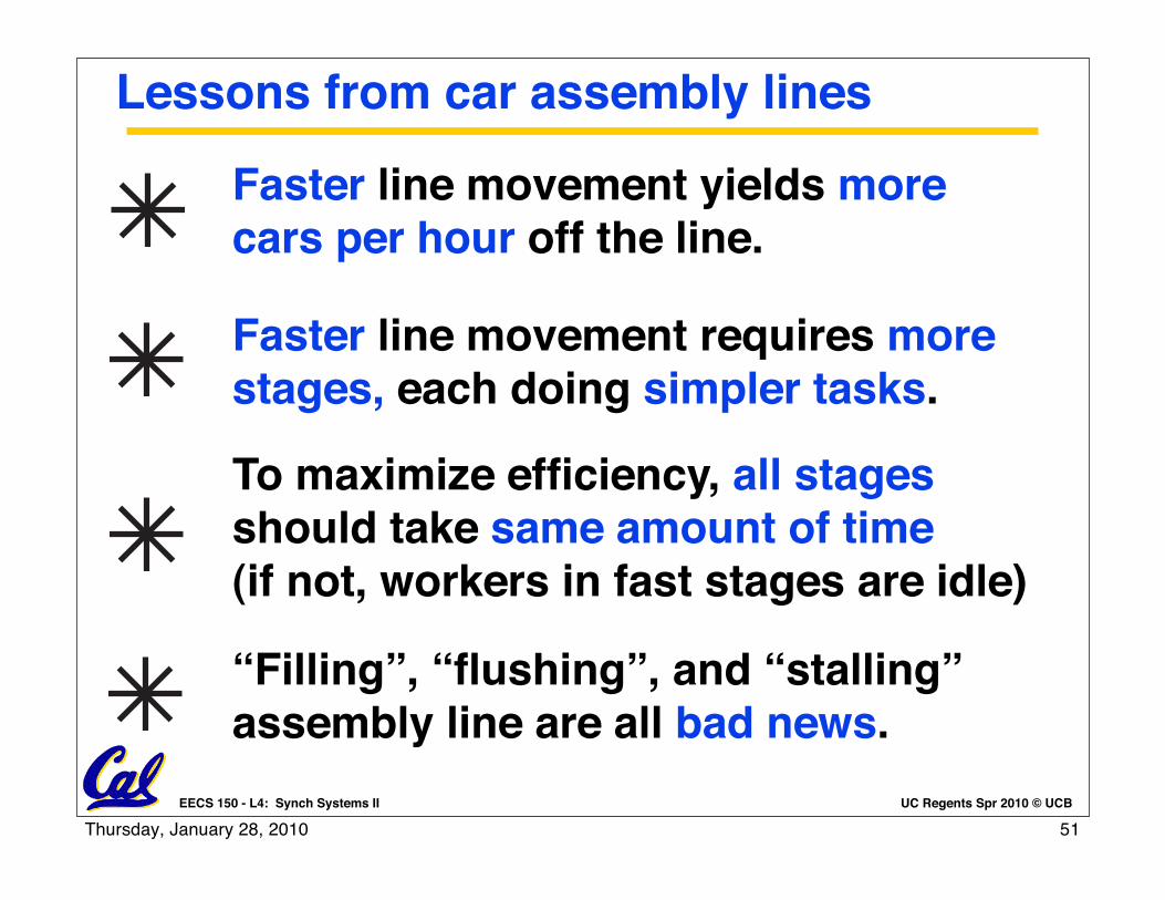
Lessons from car assembly lines
Faster line movement yields more cars per hour off the line.
Faster line movement requires more stages, each doing simpler tasks.
To maximize efficiency, all stages should take same amount of time(if not, workers in fast stages are idle)
“Filling”, “flushing”, and “stalling” assembly line are all bad news.
51Thursday, January 28, 2010

UC Regents Spr 2010 © UCBEECS 150 - L4: Synch Systems II
Flip-Flop Details
52Thursday, January 28, 2010

UC Regents Fall 2008 © UCBCS 194-6 L1: Virtex-5 Microarchitecture
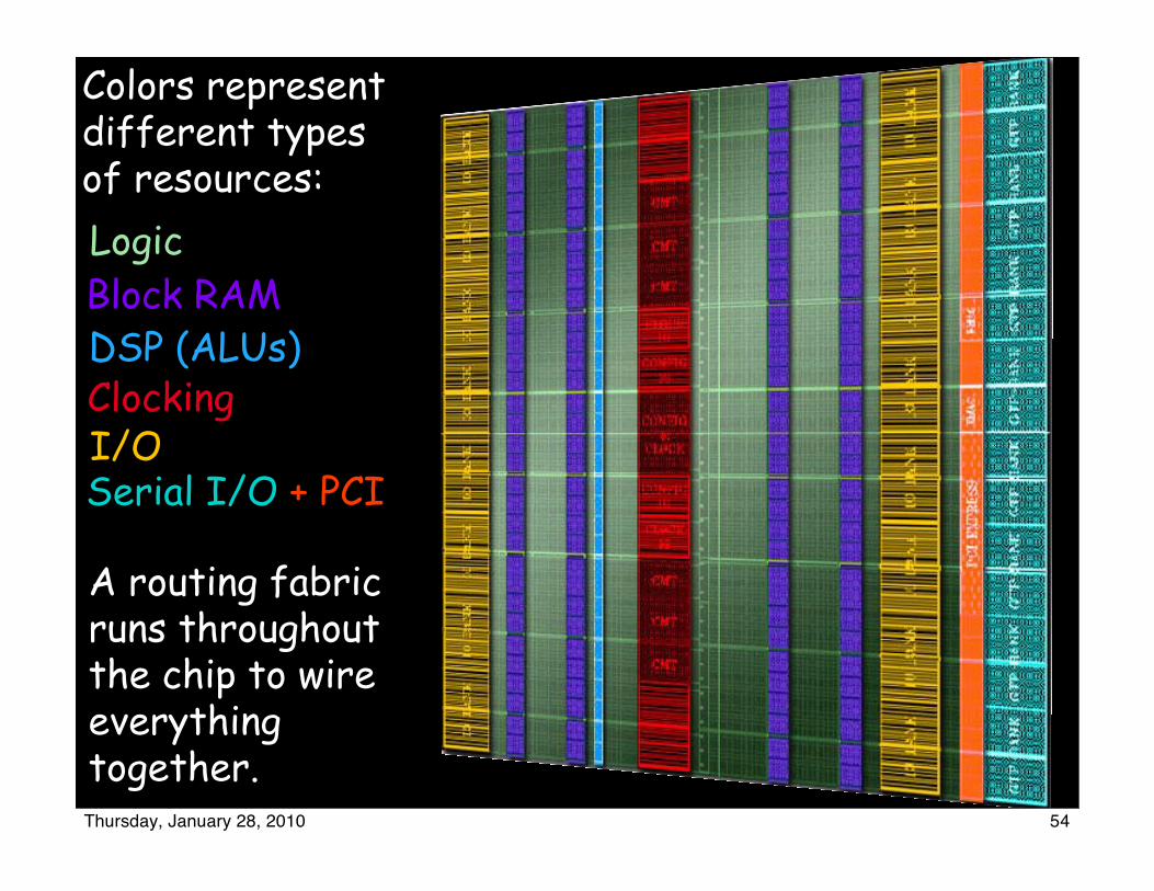
FPGA: Xilinx Virtex-5 XC5VLX110TVirtex-5 “die photo”
A die is an unpackaged part
!"#$%&'()*$$+,,-$$$).'/0$1
!"#$%&'&()*+#',$#-$./0123.445+6)*+#'7/4&6+-+6$0#895)($12#6: .(6;+*&6*9(&<
!"#$%&'()*!"#$%&'( !"#$%&')
53Thursday, January 28, 2010
UC Regents Fall 2008 © UCBCS 194-6 L1: Virtex-5 Microarchitecture
!"#$%&'()*$$+,,-$$$).'/0$1
!"#$%&'&()*+#',$#-$./0123.445+6)*+#'7/4&6+-+6$0#895)($12#6: .(6;+*&6*9(&<
!"#$%&'()*!"#$%&'( !"#$%&')
Colors represent different types of resources:LogicBlock RAMDSP (ALUs)ClockingI/OSerial I/O + PCI
A routing fabric runs throughout the chip to wire everything together.
54Thursday, January 28, 2010

UC Regents Fall 2008 © UCBCS 194-6 L1: Virtex-5 Microarchitecture
The simplest view of a slice
194 www.xilinx.com Virtex-5 FPGA User GuideUG190 (v4.2) May 9, 2008
Chapter 5: Configurable Logic Blocks (CLBs)R
Designing Large Multiplexers
4:1 Multiplexer
Each Virtex-5 LUT can be configured into a 4:1 MUX. The 4:1 MUX can be implemented with a flip-flop in the same slice. Up to four 4:1 MUXes can be implemented in a slice, as shown in Figure 5-21.
Figure 5-21: Four 4:1 Multiplexers in a Slice
UG190_5_21_050506
(D[6:1])
(C[6:1])
(B[6:1])
(A[6:1])
(CLK)CLK
6
SLICE
LUT
LUT
LUT
LUT
A[6:1]
O6
6 A[6:1]
O6
RegisteredOutput
4:1 MUX Output
(Optional)
D Q
(D)
(DQ)
RegisteredOutput
4:1 MUX Output
(Optional)
D Q
(C)
(CQ)
RegisteredOutput
4:1 MUX Output
(Optional)
D Q
(B)
(BQ)
RegisteredOutput
4:1 MUX Output
(Optional)
D Q
(A)
(AQ)
6 A[6:1]
O6
6 A[6:1]
O6
SEL D [1:0], DATA D [3:0]Input
SEL C [1:0], DATA C [3:0]Input
SEL B [1:0], DATA B [3:0]Input
SEL A [1:0], DATA A [3:0]Input
Four 6-LUTs
Four Flip-Flops
Switching fabric may see combinational and registered outputs.
55Thursday, January 28, 2010
UC Regents Fall 2008 © UCBCS 194-6 L1: Virtex-5 Microarchitecture
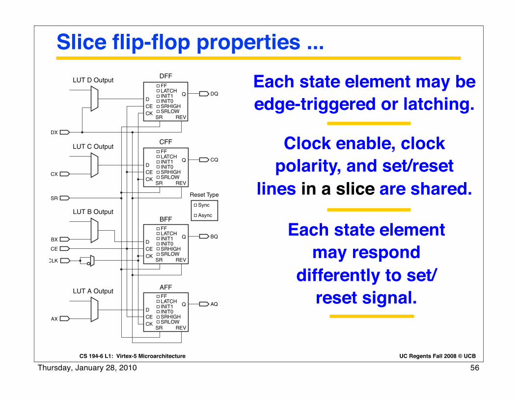
Slice flip-flop properties ...
Virtex-5 FPGA User Guide www.xilinx.com 177UG190 (v4.2) May 9, 2008
CLB OverviewR
Table 5-3: Truth Table when SRLOW is Used (Default Condition)
SR REV Function
0 0 No Logic Change
0 1 1
1 0 0
1 1 0
Table 5-4: Truth Table when SRHIGH is Used
SR REV Function
0 0 No Logic Change
0 1 0
1 0 1
1 1 0
Figure 5-5: Register/Latch Configuration in a SliceUG190_5_05_071207
DX
CX
BX
CE
AX
DQ
CQ
BQ
AQ
D
FFLATCHINIT1INIT0SRHIGHSRLOW
SR REV
DFFLUT D Output
LUT C Output
CECK
D
FFLATCHINIT1INIT0SRHIGHSRLOW
SR REV
CECK
D
FFLATCHINIT1INIT0SRHIGHSRLOW
SR REV
CECK
D
FFLATCHINIT1INIT0SRHIGHSRLOW
SR REV
Q
CECK
Q
Q
Q
SR
LUT B Output
LUT A Output AFF
BFF
CFF
CLK
Reset Type
Sync
Async
Each state element may be edge-triggered or latching.
Each state element may respond
differently to set/reset signal.
Clock enable, clock polarity, and set/reset
lines in a slice are shared.
56Thursday, January 28, 2010
Spring 2010 EECS150 lec04-SDS-review2 Page
Flip-flops on Virtex5 FPGA
57
Virtex-5 FPGA User Guide www.xilinx.com 173UG190 (v4.2) May 9, 2008
CLB OverviewR
Figure 5-3: Diagram of SLICEM
A6DI2
COUT
D
DX
C
CX
B
BX
A
AX
O6
DI1MC31
O5
UG190_5_03_041006
A5A4A3A2A1
D6
DIDMUX
D
DQ
C
CQ
CMUX
B
BQ
BMUX
A
AQ
AMUX
Reset Type
DX
D5D4D3D2D1
WA1-WA6WA7WA8
DPRAM64/32SPRAM64/32SRL32SRL16LUTRAMROM
DPRAM64/32SPRAM64/32SRL32SRL16LUTRAMROM
DPRAM64/32SPRAM64/32SRL32SRL16LUTRAMROM
DPRAM64/32SPRAM64/32SRL32SRL16LUTRAMROM
D
FFLATCHINIT1INIT0SRHIGHSRLOW
SR REV
CECK
D
FFLATCHINIT1INIT0SRHIGHSRLOW
SR REV
CECK
D
FFLATCHINIT1INIT0SRHIGHSRLOW
SR REV
CECK
D
FFLATCHINIT1INIT0SRHIGHSRLOW
SR REV
Q
CECK
CLKWSGEN
CIN
0/1
WE
Sync
Async
A6DI2
O6
DI1
MC31
O5
A5A4A3A2A1
C6
CI
CX
C5C4C3C2C1
A6DI2
O6
DI1
MC31
O5
A5A4A3A2A1
B6
BI
BX
B5B4B3B2B1
A6DI2
O6
DI1
MC31
O5
A5A4A3A2A1
A6
AI
AXSRCE
CLK
WE
A5A4A3A2A1
Q
Q
Q
WA1-WA6WA7WA8
WA1-WA6WA7WA8
WA1-WA6WA7WA8
174 www.xilinx.com Virtex-5 FPGA User GuideUG190 (v4.2) May 9, 2008
Chapter 5: Configurable Logic Blocks (CLBs)R
Each CLB can contain zero or one SLICEM. Every other CLB column contains a SLICEMs. In addition, the two CLB columns to the left of the DSP48E columns both contain a SLICEL and a SLICEM.
Figure 5-4: Diagram of SLICEL
A6LUTROM
COUT
D
DX
C
CX
B
BX
A
AX
O6O5
UG190_5_04_032606
A5A4A3A2A1
D6
DMUX
D
DQ
C
CQ
CMUX
B
BQ
BMUX
A
AQ
AMUX
DX
D5D4D3D2D1
D
FFLATCHINIT1INIT0SRHIGHSRLOW
SR REV
CECK
D
FFLATCHINIT1INIT0SRHIGHSRLOW
SR REV
CECK
D
FFLATCHINIT1INIT0SRHIGHSRLOW
SR REV
CECK
D
FFLATCHINIT1INIT0SRHIGHSRLOW
SR REV
Q
CECK
CIN
0/1
A6LUTROM
O6O5
A5A4A3A2A1
C6
CX
C5C4C3C2C1
A6LUTROM
O6O5
A5A4A3A2A1
B6
BX
B5B4B3B2B1
A6LUTROM
O6O5
A5A4A3A2A1
A6
AXSRCE
CLK
A5A4A3A2A1
Q
Q
Q
Reset Type
Sync
Async
SLICEMSLICEL
37
Other flip-flops in the chip input/output cells, and in the form of registers in the DSP slices and memory block interfaces.
Four flip-flops per 17,280 slices in
an LX110T.
57Thursday, January 28, 2010

Spring 2010 EECS150 lec04-SDS-review2 Page
Virtex5 Slice Flip-flops
58
4 flip-flops / slice (corresponding to the 4 6-LUTs)
Each takes input from LUT output or primary slice input.
Edge-triggered FF vs. level-sensitive latch.Clock-enable input (can be set to 1 to disable) (shared).Positive versus negative clock-edge.Synchronous vs. asynchronous reset.SRHIGH/SRLOW select reset (SR) set.REV forces opposite state.INIT0/INIT1 used for global reset (not shown - usually just after power-on and configuration).
58Thursday, January 28, 2010
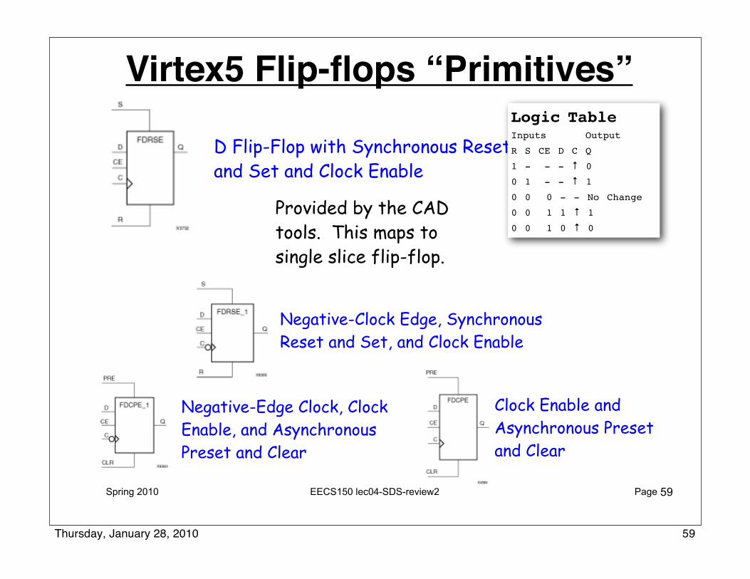
Spring 2010 EECS150 lec04-SDS-review2 Page
Virtex5 Flip-flops “Primitives”
59
Clock Enable and Asynchronous Preset and Clear
Negative-Edge Clock, Clock Enable, and Asynchronous Preset and Clear
D Flip-Flop with Synchronous Reset and Set and Clock Enable
D Flip-Flop with Synchronous Reset and Set and Clock Enable
Negative-Clock Edge, Synchronous Reset and Set, and Clock Enable
Logic Table Inputs Output R S CE D C Q 1 - - - ↑ 0 0 1 - - ↑ 1 0 0 0 - - No Change 0 0 1 1 ↑ 1 0 0 1 0 ↑ 0
Provided by the CAD tools. This maps to single slice flip-flop.
59Thursday, January 28, 2010

UC Regents Spr 2010 © UCBEECS 150 - L4: Synch Systems II
Inside a Flip-Flop
60Thursday, January 28, 2010
Spring 2010 EECS150 lec04-SDS-review2 Page
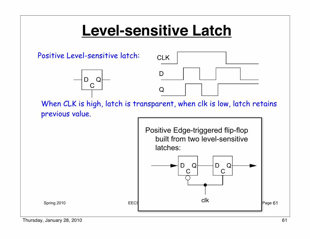
Level-sensitive LatchPositive Level-sensitive latch:
Positive Edge-triggered flip-flop built from two level-sensitive latches:
61
When CLK is high, latch is transparent, when clk is low, latch retains previous value.
61Thursday, January 28, 2010

UC Regents Spr 2010 © UCBEECS 150 - L4: Synch Systems II
Upcoming events:
Have a good weekend!
62Thursday, January 28, 2010