ee 434 lecture 42
TRANSCRIPT

EE 434Lecture 42
Other Logic Styles
Static CMOS LogicComplex Logic GatesPass Transistor LogicPseudo-NMOSDynamic Logic

Review from last time
DD
IN
PU Network
PD Network
Complex Logic Gates
Implement in PD Network with n-channel devicesF
Implement in PU Network with p-channel devices with complimented variablesF
Preserves rail-to-rail signal swingNo static power dissipationAt most two levels of logicOften significant reduction in device count and delay

Review from last time
Pass Transistor Logic
Low device count implementation of non inverting function (can be dramatic)Logic Swing not rail to rail Static power dissipation not 0 when F highRLG may be unacceptably largeSlow tLHSignal degradation can occur when multiple levels of logic are used
DD
LG
Example:
F=A•B

Review from last time
Pass Transistor Logic
LG
RLG RLG RLG
SMALL
Physical Size of RLG too large
Methods of implementing RLG

Review from last time
Pass Transistor Logic
Signal degradation No signal degradation
Signal degradation may occur with PTL
A
B F
RLG
D
RLG
• Can intermix n-channel and p-channel devices to reduce/eliminate the signal degradation problem • Can add static CMOS buffers to restore signals provided too much signal degradation has not occured

Other Logic Styles
Static CMOS LogicComplex Logic GatesPass Transistor LogicPseudo-NMOSDynamic Logic

Pass Transistor Logic Gates

Pass Transistor Logic Gates
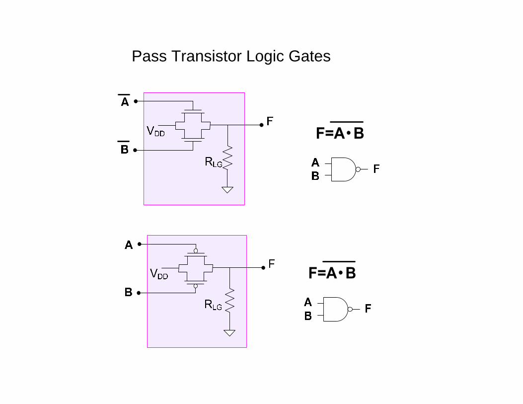
Pass Transistor Logic Gates

Pass Transistor Logic Gates

Pass Transistor Logic Gates

Pass Transistor Logic Gates
DD
IN
PU Network
LG
• Observe all PTL gates discussed so far were of this form• PU network can contain a mixture of n-channel and p-channel devices• Any of the PU networks used for complex logic gates could also be
used in PTL

Pass Transistor Logic Gates
• PTL gates could also be designed with logic in PD network • PD network can contain a mixture of n-channel and p-channel devices• Any of the PD networks used in complex logic gates could be used in PTL
DD
IN
PD Network
LG

Pass Transistor Logic Gates VDD
FXIN
PD Network
RLG
As an example:

Other Logic Styles
Static CMOS LogicComplex Logic GatesPass Transistor LogicPseudo-NMOSDynamic Logic

Dynamic LogicDD
IN
PU Network
PD Network
VDD
FXIN
PU Network
RLG
PU network major contributor to dynamic power dissipationPU network for complex logic gates requires large devices for good tLHPU network requires large area for n-wellsPU and PD network duplicate logic function
Observations:

Dynamic LogicDD
IN
PU Network
PD Network
VDD
FXIN
PU Network
RLG
Is it possible to eliminate PU Network and still maintain signal swing and zero static power dissipation of complex logic gate approaches?
Question:

Dynamic Logic
PD Network
CH
IN
CLK
VDD
CLK
Basic Dynamic Logic Gate
Precharges F to VDD when CLK is low (precharge state)
when CLK is high (evaluate state) discharges CH only if PD network conducts
CH (hold capacitor) can be simply parasitic capacitances on node F

Dynamic Logic
Basic Dynamic Logic Gate
• Potential for substantial decrease in dynamic power dissipation• Zero Static Power Dissipation• Excellent speed• Reduced area
PD Network
CH
IN
CLK
VDD
CLK
Positive Attributes:

Dynamic Logic
• Output valid only during evaluate state• Requires Clock • Can not be placed in a static hold state• Premature discharge can occur with cascaded logic (potential stopper !)
PD Network 1
CH
IN1
CLK
VDD
CLK
PD Network 2
CH
CLK
VDD
CLK
IN2
Negative Attributes:

Dynamic Logic
CH
CLK
VDD
CLK
CH
CLK
VDD
CLK
A
B
Premature discharge example:
When G is precharged high and is to go Low (A=B=1) on the evaluate stateF should be a 1 but may be prematurely discharged while G is high
Alternatively, if A or B are to be 1 but come from another gate where they were low initially, there may be a delay for becoming 1 thus keeping G high even longer thus prematurely discharging F