ecen 248: introduction to digital systems...
TRANSCRIPT
ECEN 248: INTRODUCTION TO DIGITAL SYSTEMS DESIGN
Week 1 Dr. Srinivas Shakkottai Dept. of Electrical and Computer Engineering
Instructor:
¨ Dr. Srinivas Shakkottai ! Office 332C WEB ! Office Hours: Wed 2:00PM-3:00 PM, Fri 2:00 PM – 3:00 PM ! Email: User: sshakkot at Domain: tamu.edu ! Lab Timings: check section ! No lab this week.

Required textbook:
¨ Brown and Vranesic (3rd Edition) Fundamentals of Digital Logic with Verilog
Design.

Reference textbook:
¨ "Digital Design: Principles and Practices" by John Wakerly.
¨ "Contemporary Logic Design” by Randy Katz.

Course info
¨ Mailing list: ! Emails will be sent periodically to tamu accounts ! Announcements:
n Lecture cancellations n Deadline extension n Updates, etc.
¨ Course website ! http://cesg.tamu.edu/courses/ecen-248-digital-
systems-design/ ! All slides, labs, assignments, etc.
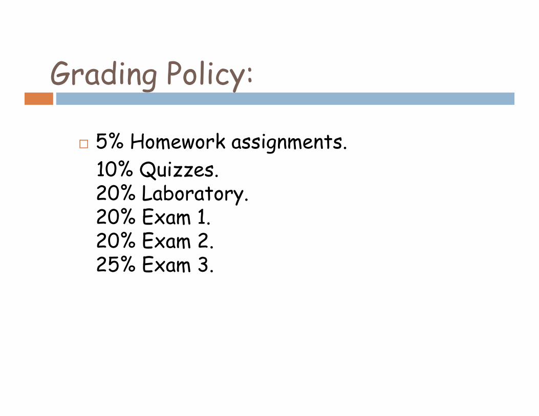
Grading Policy:
¨ 5% Homework assignments. 10% Quizzes.
20% Laboratory. 20% Exam 1. 20% Exam 2. 25% Exam 3.

Grading scale
¨ A standard grading scale will be utilized. The tentative grading scale for the course is: ¨ A 90-100% ¨ B 80-89% ¨ C 70-79% ¨ D 60-69% ¨ F Below 59%

Course Goals
¨ Study methods for ! Representation, manipulation, and optimization for
both combinatorial and sequential logic ! Solving digital design problems ! Study HDL description language (Verilog)

Topics
¨ Number bases ¨ Logic gates and Boolean Algebra ¨ Gate–level minimization ¨ Combinational Logic ¨ Sequential logic (Latches, Flip-flops,
Registers, and Counters) ¨ Memory and Programmable Logic ¨ HDL language (Verilog)

Verilog
¨ Stands for Verify Logic. ¨ Verilog Hardware Description Language. ¨ Procedure is to use a compiler for
compiling source code written in Verilog. ¨ Subset of statements can be synthesized
using logic circuits.
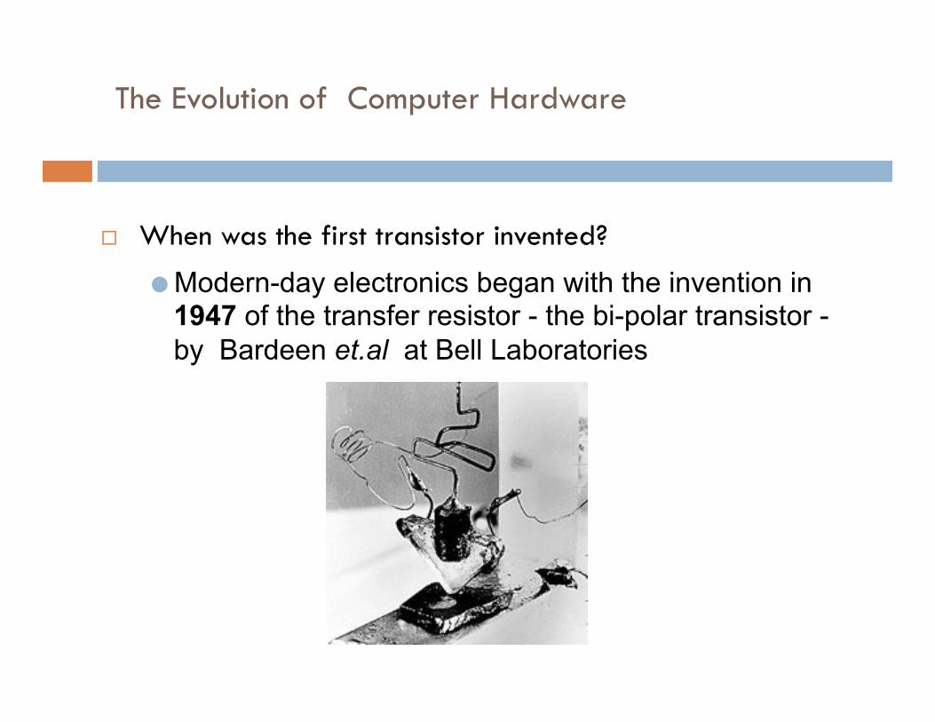
The Evolution of Computer Hardware
¨ When was the first transistor invented? ● Modern-day electronics began with the invention in
1947 of the transfer resistor - the bi-polar transistor - by Bardeen et.al at Bell Laboratories

The Evolution of Computer Hardware
¨ When was the first IC (integrated circuit) invented?
● In 1958 the IC was born when Jack Kilby at Texas Instruments successfully interconnected, by hand, several transistors, resistors and capacitors on a single substrate
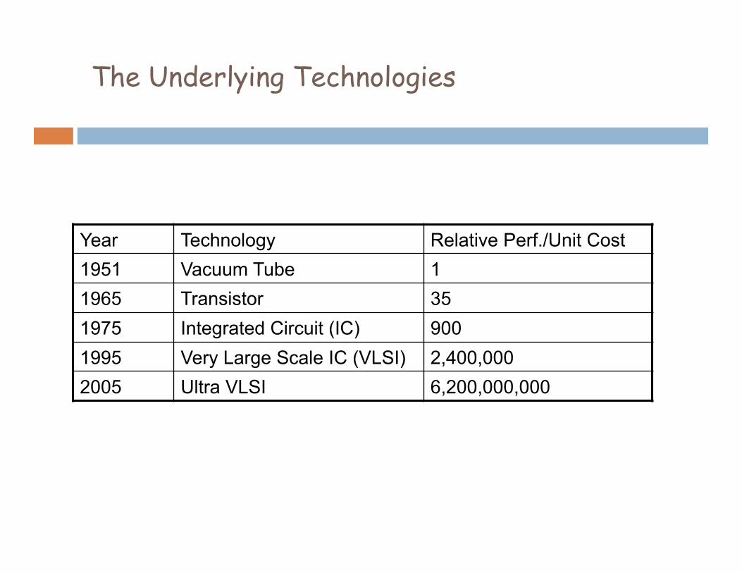
The Underlying Technologies
Year Technology Relative Perf./Unit Cost 1951 Vacuum Tube 1 1965 Transistor 35 1975 Integrated Circuit (IC) 900 1995 Very Large Scale IC (VLSI) 2,400,000 2005 Ultra VLSI 6,200,000,000

The PowerPC 750
¨ Introduced in 1999 ¨ 3.65M transistors ¨ 366 MHz clock rate ¨ 40 mm2 die size ¨ 250nm technology
ECEN 248
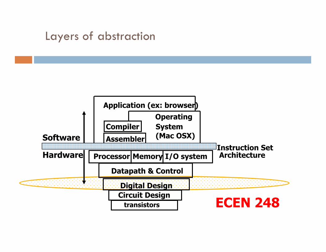
Layers of abstraction
I/O system Processor
Compiler Operating System (Mac OSX)
Application (ex: browser)
Digital Design Circuit Design
Instruction Set Architecture
Datapath & Control
transistors
Memory Hardware
Software Assembler
Year
Tran
sisto
rs
1000
10000
100000
1000000
10000000
100000000
1970 1975 1980 1985 1990 1995 2000
i80386
i4004
i8080
Pentium
i80486
i80286
i8086
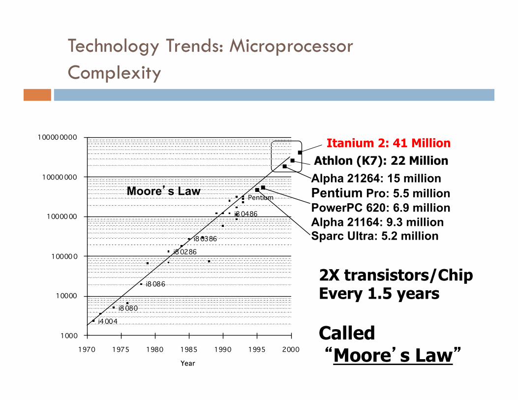
Technology Trends: Microprocessor Complexity
2X transistors/Chip Every 1.5 years
Called “Moore’s Law”
Alpha 21264: 15 million Pentium Pro: 5.5 million PowerPC 620: 6.9 million Alpha 21164: 9.3 million Sparc Ultra: 5.2 million
Moore’s Law
Athlon (K7): 22 Million Itanium 2: 41 Million
NUMBER SYSTEMS

Overview
¨ Understanding decimal numbers ¨ Binary and octal numbers
! The basis of computers!
¨ Conversion between different number systems

Digital Computer Systems
¨ Digital systems consider discrete amounts of data. ¨ Examples
! 26 letters in the alphabet ! 10 decimal digits
¨ Larger quantities can be built from discrete values: ! Words made of letters ! Numbers made of decimal digits (e.g. 239875.32)
¨ Computers operate on binary values (0 and 1) ¨ Easy to represent binary values electrically
! Voltages and currents. ! Can be implemented using circuits ! Create the building blocks of modern computers

Understanding Decimal Numbers
¨ Decimal numbers are made of decimal digits: (0,1,2,3,4,5,6,7,8,9)
¨ Number representation: ! 8653 = 8x10³ + 6x10² + 5x101 + 3x100
¨ What about fractions? ! 97654.35 = 9x10⁴ + 7x10³ + 6x10² + 5x101 + 4x100 +
3x10⁻¹ + 5x10⁻²
! Informal notation à (97654.35)10

Understanding Octal Numbers
¨ Octal numbers are made of octal digits: (0,1,2,3,4,5,6,7)
¨ Number representation: ! (4536)8 = 4x83 + 5x82 + 3x81 + 6x80 = (2398)10
¨ What about fractions? ! (465.27)8 = 4x82 + 6x81 + 5x80 + 2x8-1 + 7x8-2
¨ Octal numbers don’t use digits 8 or 9
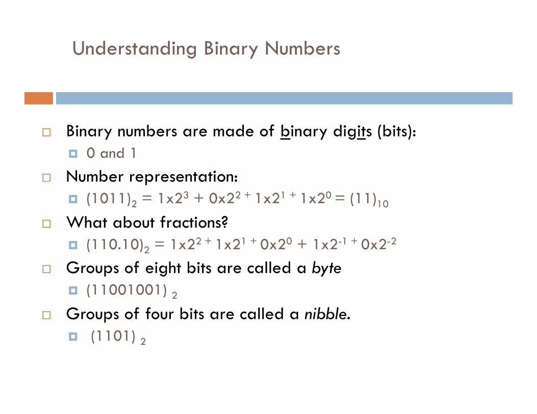
Understanding Binary Numbers
¨ Binary numbers are made of binary digits (bits): ! 0 and 1
¨ Number representation: ! (1011)2 = 1x23 + 0x22 + 1x21 + 1x20 = (11)10
¨ What about fractions? ! (110.10)2 = 1x22 + 1x21 + 0x20 + 1x2-1 + 0x2-2
¨ Groups of eight bits are called a byte ! (11001001) 2
¨ Groups of four bits are called a nibble. ! (1101) 2

Why Use Binary Numbers?
° Easy to represent 0 and 1 using electrical values.
° Possible to tolerate noise.
° Easy to transmit data
° Easy to build binary circuits.
AND Gate
1
0 0
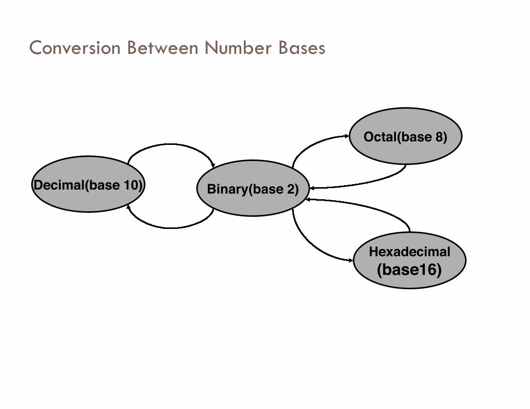
Conversion Between Number Bases
Decimal(base 10)!
Octal(base 8)!
Binary(base 2)!
Hexadecimal!(base16)!
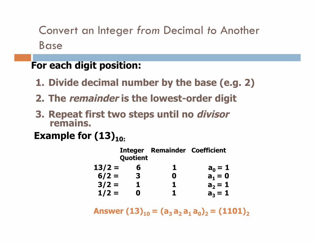
Convert an Integer from Decimal to Another Base
1. Divide decimal number by the base (e.g. 2)
2. The remainder is the lowest-order digit
3. Repeat first two steps until no divisor remains.
For each digit position:
Example for (13)10:
Integer Quotient
13/2 = 6 1 a0 = 1 6/2 = 3 0 a1 = 0 3/2 = 1 1 a2 = 1 1/2 = 0 1 a3 = 1
Remainder Coefficient
Answer (13)10 = (a3 a2 a1 a0)2 = (1101)2
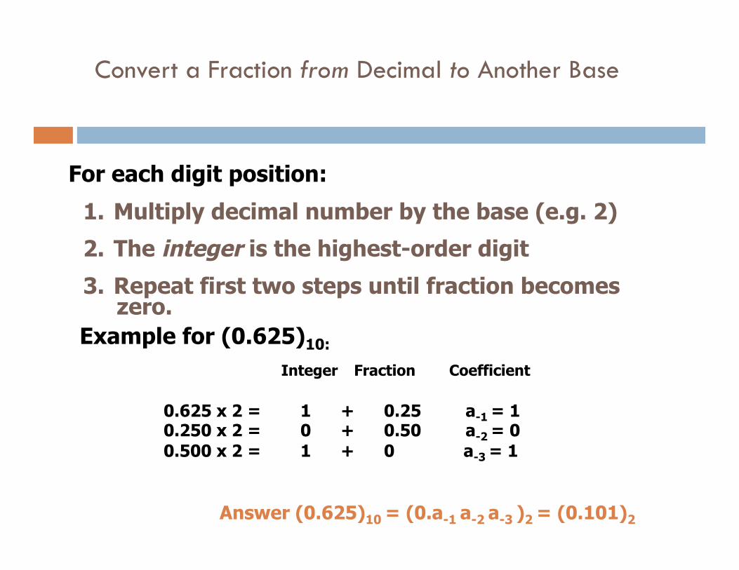
Convert a Fraction from Decimal to Another Base
1. Multiply decimal number by the base (e.g. 2)
2. The integer is the highest-order digit
3. Repeat first two steps until fraction becomes zero.
For each digit position:
Example for (0.625)10:
Integer
0.625 x 2 = 1 + 0.25 a-1 = 1 0.250 x 2 = 0 + 0.50 a-2 = 0 0.500 x 2 = 1 + 0 a-3 = 1
Fraction Coefficient
Answer (0.625)10 = (0.a-1 a-2 a-3 )2 = (0.101)2
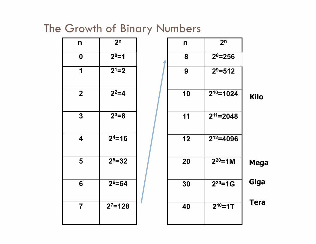
The Growth of Binary Numbers n 2n
0 20=1
1 21=2
2 22=4
3 23=8
4 24=16
5 25=32
6 26=64
7 27=128
n 2n
8 28=256
9 29=512
10 210=1024
11 211=2048
12 212=4096
20 220=1M
30 230=1G
40 240=1T
Mega
Giga
Tera
Kilo

Binary Arithmetic
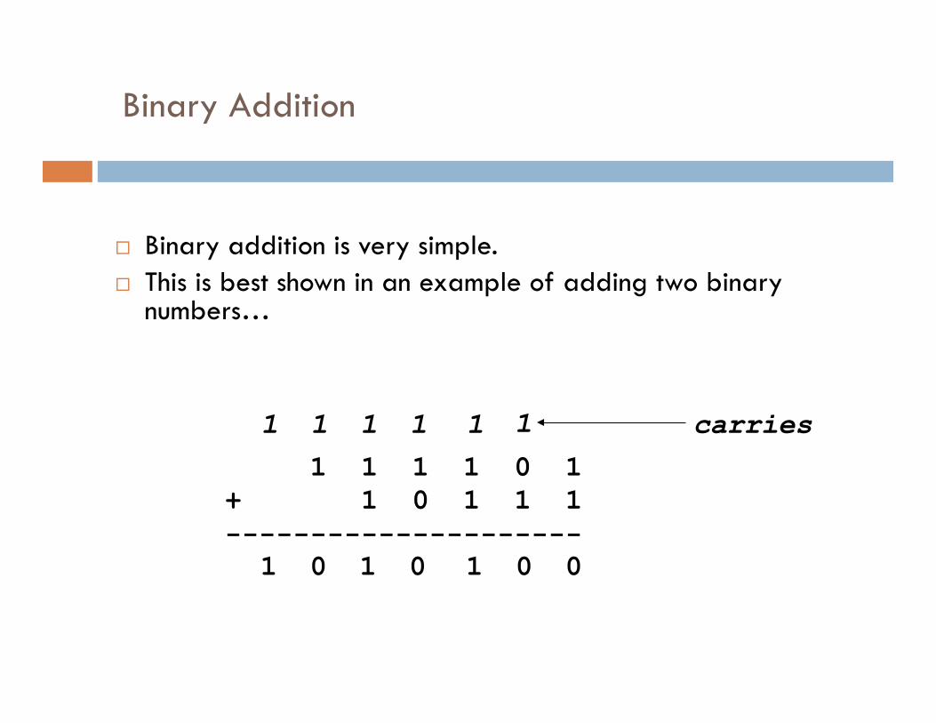
Binary Addition
¨ Binary addition is very simple. ¨ This is best shown in an example of adding two binary
numbers…
1 1 1 1 0 1 + 1 0 1 1 1 ---------------------
0
1
0
1
1
1 1 1 1
1 1 0 0
carries

Binary Subtraction
° We can also perform subtraction (with borrows in place of carries).
° Let’s subtract (10111)2 from (1001101)2…
1 10 0 10 10 0 0 10
1 0 0 1 1 0 1
- 1 0 1 1 1 ------------------------ 1 1 0 1 1 0
borrows

Binary Multiplication
¨ Binary multiplication is much the same as decimal multiplication, except that the multiplication operations are much simpler…
1 0 1 1 1 X 1 0 1 0 ----------------------- 0 0 0 0 0 1 0 1 1 1 0 0 0 0 0 1 0 1 1 1 ----------------------- 1 1 1 0 0 1 1 0
Digital Systems
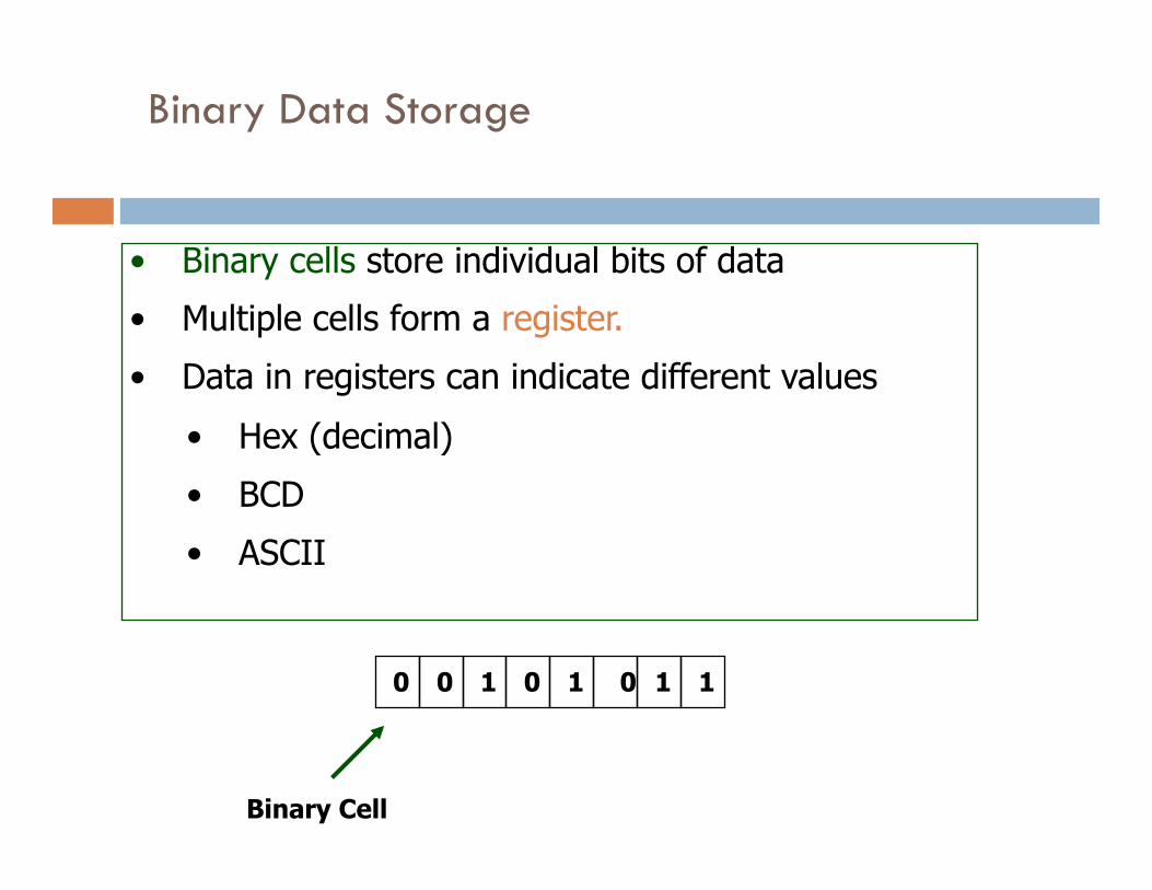
Binary Data Storage
• Binary cells store individual bits of data
• Multiple cells form a register.
• Data in registers can indicate different values
• Hex (decimal)
• BCD
• ASCII
Binary Cell
0 0 1 0 1 0 1 1
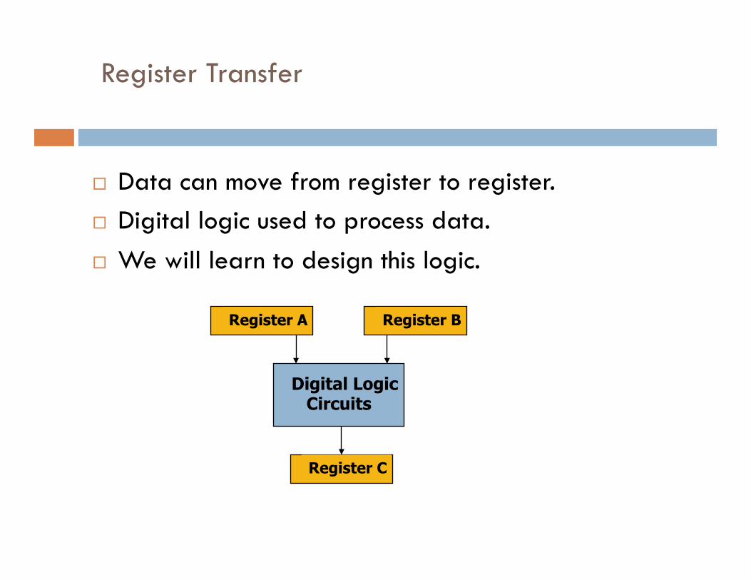
Register Transfer
¨ Data can move from register to register. ¨ Digital logic used to process data. ¨ We will learn to design this logic.
Register A Register B
Register C
Digital Logic Circuits
Digital Systems
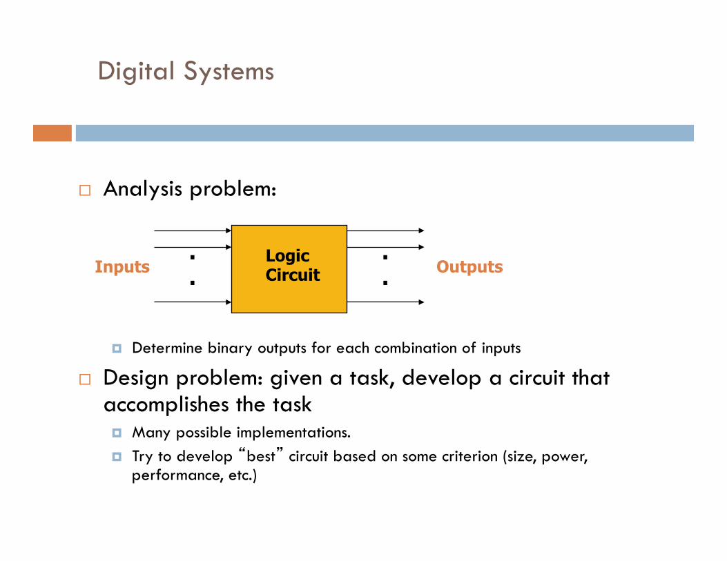
¨ Analysis problem:
! Determine binary outputs for each combination of inputs
¨ Design problem: given a task, develop a circuit that accomplishes the task ! Many possible implementations. ! Try to develop “best” circuit based on some criterion (size, power,
performance, etc.)
· ·
· ·
Logic Circuit Inputs Outputs

Toll Booth Controller
¨ Consider the design of a toll booth controller. ¨ Inputs: quarter, car sensor. ¨ Outputs: gate lift signal, gate close signal
¨ If driver pitches in quarter, raise gate. ¨ When car has cleared gate, close gate.
Logic Circuit
$·25
Car?
Raise gate
Close gate

Gates

Describing Circuit Functionality: Inverter
¨ Basic logic functions have symbols. ¨ The same functionality can be represented with truth
tables·∙ ! Truth table completely specifies outputs for all input
combinations. ¨ The above circuit is an inverter.
! An input of 0 is inverted to a 1. ! An input of 1 is inverted to a 0.
A Y
0 1
1 0
Input Output
A Y
Symbol
Truth Table

The AND Gate
¨ This is an AND gate. ¨ So, if the two inputs signals
are asserted (high) the output will also be asserted. Otherwise, the output will be deasserted (low).
A B Y
0 0 0
0 1 0
1 0 0
1 1 1
A
B Y
Truth Table
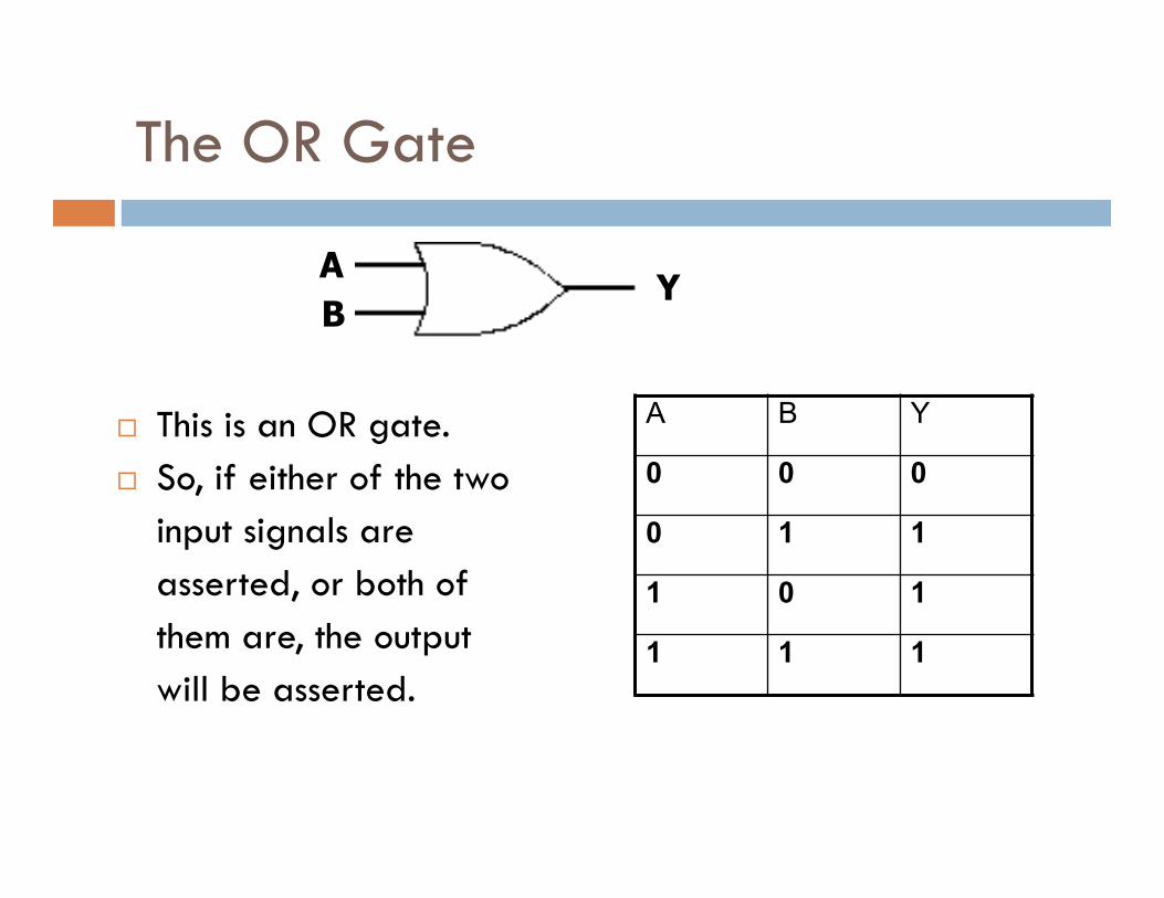
The OR Gate
¨ This is an OR gate. ¨ So, if either of the two
input signals are asserted, or both of them are, the output will be asserted.
A B Y
0 0 0
0 1 1
1 0 1
1 1 1
A B
Y
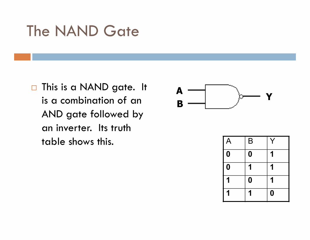
The NAND Gate
¨ This is a NAND gate. It is a combination of an AND gate followed by an inverter. Its truth table shows this. A B Y
0 0 1 0 1 1 1 0 1 1 1 0
A B
Y
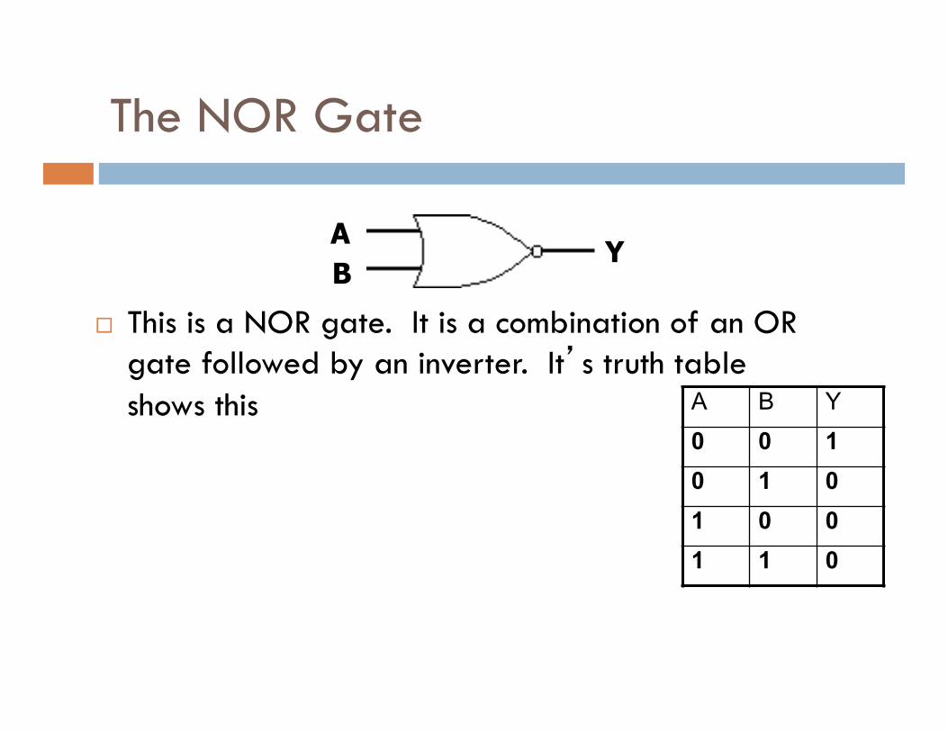
The NOR Gate
¨ This is a NOR gate. It is a combination of an OR gate followed by an inverter. It’s truth table shows this A B Y
0 0 1 0 1 0 1 0 0 1 1 0
A B
Y
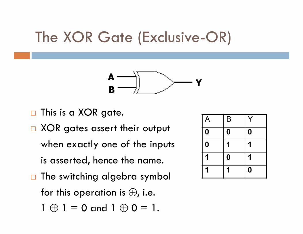
The XOR Gate (Exclusive-OR)
¨ This is a XOR gate. ¨ XOR gates assert their output
when exactly one of the inputs is asserted, hence the name.
¨ The switching algebra symbol for this operation is ⊕, i.e. 1 ⊕ 1 = 0 and 1 ⊕ 0 = 1.
A B Y 0 0 0 0 1 1 1 0 1 1 1 0
A B
Y

Describing Circuit Functionality: Waveforms
¨ Waveforms provide another approach for representing functionality.
¨ Values are either high (logic 1) or low (logic 0). ¨ Can you create a truth table from the waveforms?
A B Y 0 0 0 0 1 0 1 0 0 1 1 1
AND Gate

Consider three-input gates
3 Input OR Gate
Ordering Boolean Functions
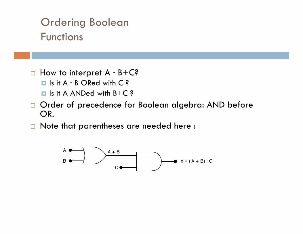
¨ How to interpret A ·∙ B+C? ! Is it A ·∙ B ORed with C ? ! Is it A ANDed with B+C ?
¨ Order of precedence for Boolean algebra: AND before OR.
¨ Note that parentheses are needed here :