ece 551 fall 2001 19/6/2001 ece 551 - digital system design & synthesis lecture 2 - pragmatic...
TRANSCRIPT
ECE 551 Fall 2001 19/6/2001
ECE 551 - Digital System Design & Synthesis
Lecture 2 - Pragmatic Design IssuesPart 2
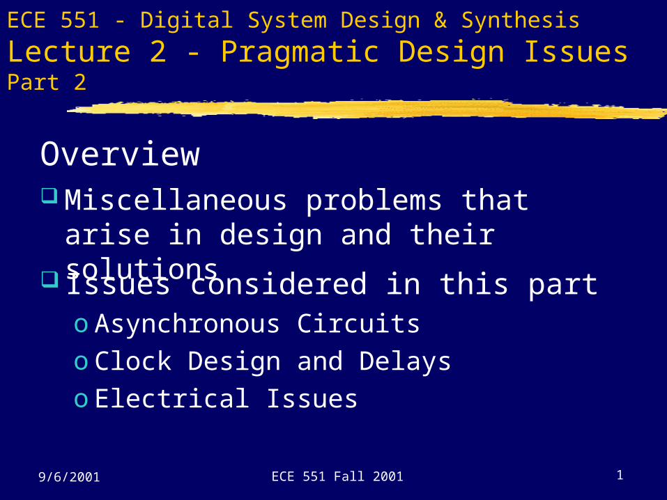
Overview
Issues considered in this parto Asynchronous Circuitso Clock Design and Delayso Electrical Issues
Miscellaneous problems that arise in design and their solutions

ECE 551 Fall 2001 29/6/2001
Asynchronous Circuits
Delay-dependent design Combinational hazards Level/pulse conversion Synchronization Memory timing
ECE 551 Fall 2001 39/6/2001
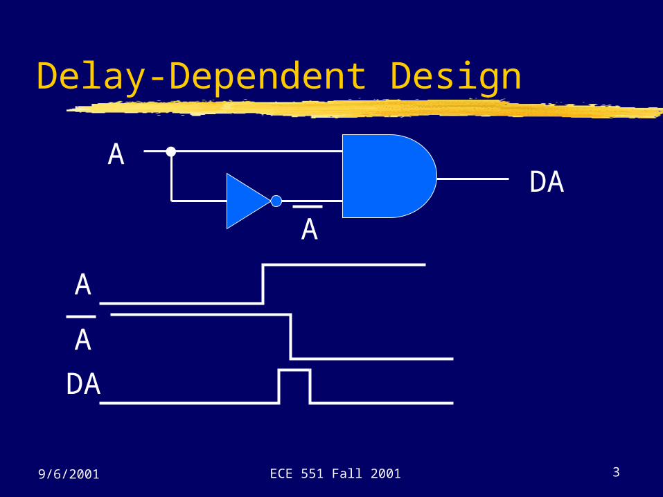
Delay-Dependent Design
ADA
A
A
A
DA
ECE 551 Fall 2001 49/6/2001
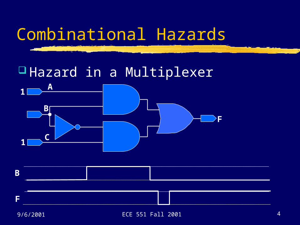
Combinational Hazards
Hazard in a MultiplexerA
C
FB
1
1
B
F
ECE 551 Fall 2001 59/6/2001
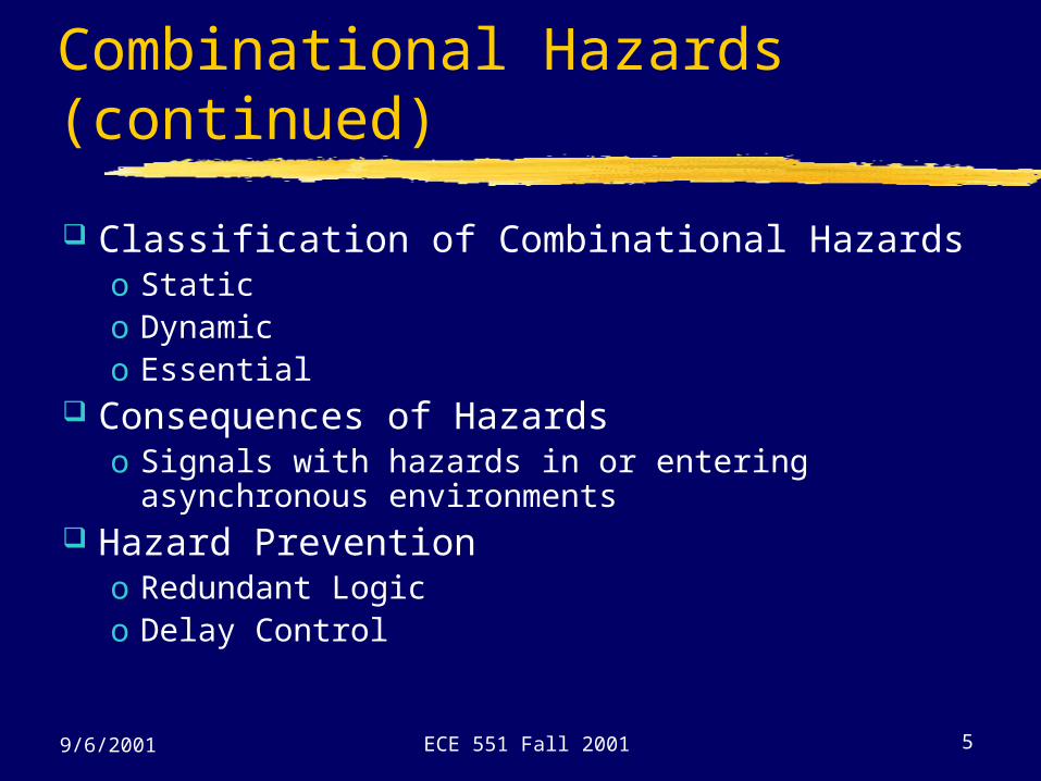
Combinational Hazards (continued)
Classification of Combinational Hazardso Statico Dynamico Essential
Consequences of Hazardso Signals with hazards in or entering
asynchronous environments Hazard Prevention
o Redundant Logico Delay Control
ECE 551 Fall 2001 69/6/2001
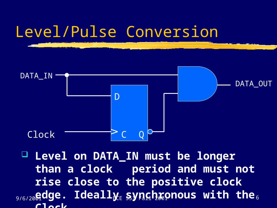
Level/Pulse Conversion
DATA_INDATA_OUT
D
QCClock
Level on DATA_IN must be longer than a clock period and must not rise close to the positive clock edge. Ideally synchronous with the Clock.

ECE 551 Fall 2001 79/6/2001
Synchronization
D Q
CClock
D Q
C
Req Rep
Clock
Asynchronous Rep can cause sequential circuit malfunction since it reaches two or more flip-flops.
Solution: Put synchronizer (PET DFF) in Rep path.
ECE 551 Fall 2001 89/6/2001
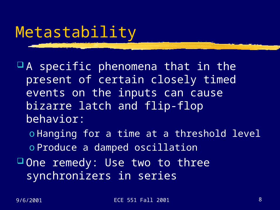
Metastability
A specific phenomena that in the present of certain closely timed events on the inputs can cause bizarre latch and flip-flop behavior:o Hanging for a time at a threshold levelo Produce a damped oscillation
One remedy: Use two to three synchronizers in series

ECE 551 Fall 2001 99/6/2001
Memory Timing
Many memories are asynchronous circuits, e. g., SRAMs are latch-based without a clock on the latcho Their inputs can respond to “glitches” such as hazards.o A majority of all memory inputs need to be “glitch-free.”
Since memories involve capture of data in selectively-addressed cells, set-up and hold times apply to many of the inputs, notably the addresses.
Memory outputs often involve 3-state buses; one must be sure that the bus is active whenever data is being read.
When designing with memories, careful attention must be given to meeting fully all of the timing specifications.
ECE 551 Fall 2001 109/6/2001
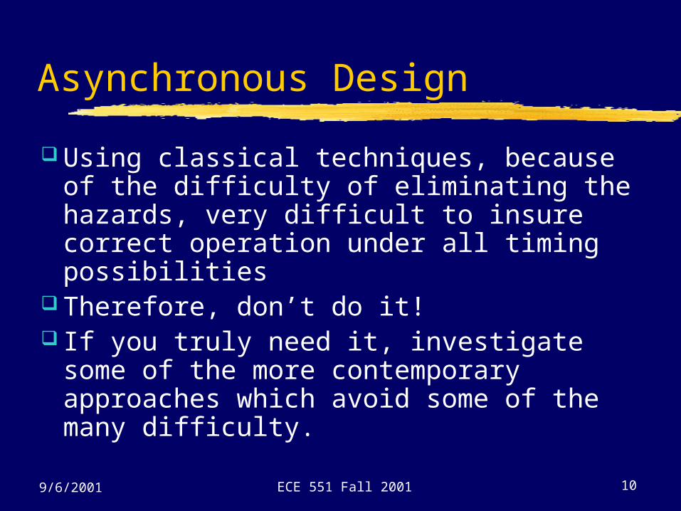
Asynchronous Design
Using classical techniques, because of the difficulty of eliminating the hazards, very difficult to insure correct operation under all timing possibilities
Therefore, don’t do it! If you truly need it, investigate some
of the more contemporary approaches which avoid some of the many difficulty.
ECE 551 Fall 2001 119/6/2001
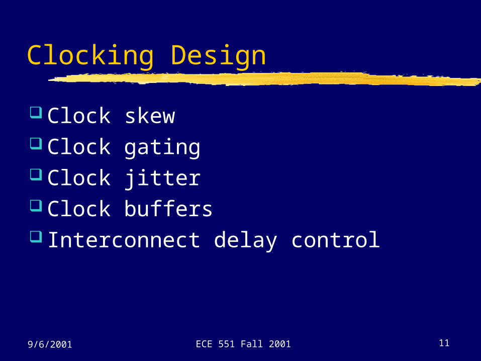
Clocking Design
Clock skew Clock gating Clock jitter Clock buffers Interconnect delay control
ECE 551 Fall 2001 129/6/2001
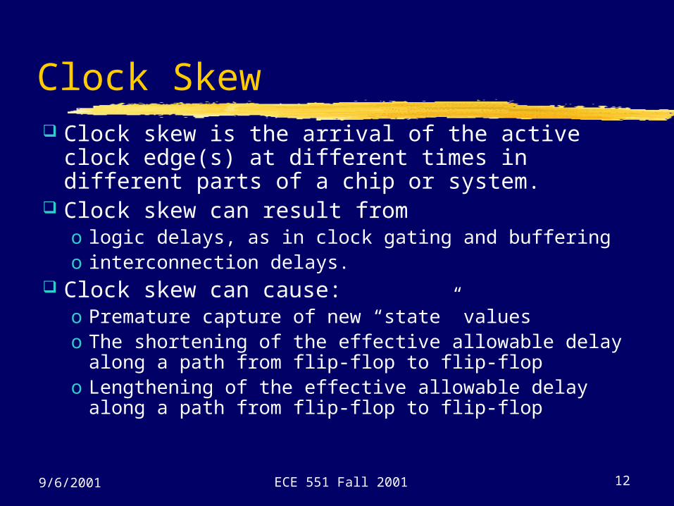
Clock Skew Clock skew is the arrival of the active clock
edge(s) at different times in different parts of a chip or system.
Clock skew can result from o logic delays, as in clock gating and bufferingo interconnection delays.
Clock skew can cause:o Premature capture of new “state” valueso The shortening of the effective allowable delay along
a path from flip-flop to flip-flopo Lengthening of the effective allowable delay along a
path from flip-flop to flip-flop

ECE 551 Fall 2001 139/6/2001
Clock Gating
Use of gate logic to interrupt the clock signal to a portion of the logic to prevent the state from changing
Why use it?o Simplifies logico Reduces power consumption
Why not use it?o Can circuit failure due to clock skewo Complicates circuit testing
ECE 551 Fall 2001 149/6/2001
Clock Jitter
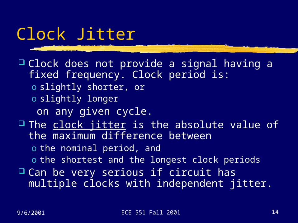
Clock does not provide a signal having a fixed frequency. Clock period is:o slightly shorter, or o slightly longer
on any given cycle. The clock jitter is the absolute value of the
maximum difference betweeno the nominal period, ando the shortest and the longest clock periods
Can be very serious if circuit has multiple clocks with independent jitter.

ECE 551 Fall 2001 159/6/2001
Combinational Logic Delay Upper Bound
Components of the Boundso Nominal Clock Period CPo FF Propagation Delay tFF
o FF Set-up Time tSU
o Clock skew (of destination FF clock with respect to source FF clock) (+ or –) tsc
o Clock Jitter Magnitude tCJ
Combinational Logic Delay Upper Bound along Particular FF to FF path:o DCL < CP + tsc – tCJ – tFF – tSU
From this equation, we see that:o Clock jitter degrades performanceo Clock skew may either degrade (if negative) or enhance (if
positive) performance!
ECE 551 Fall 2001 169/6/2001
Combinational Logic Delay Lower Bound
Related to incorrect function due to hold time violation
Left as an exercise
ECE 551 Fall 2001 179/6/2001
Clock Buffers
Reasons for bufferingo Large driven loado Long clock interconnects
Must be designed to minimize skew Overall, clock distribution in an
aggressive design is a major separate task
ECE 551 Fall 2001 189/6/2001
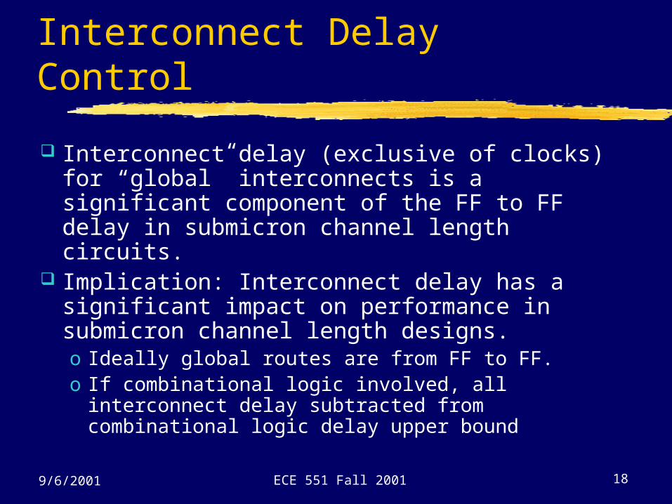
Interconnect Delay Control
Interconnect delay (exclusive of clocks) for “global” interconnects is a significant component of the FF to FF delay in submicron channel length circuits.
Implication: Interconnect delay has a significant impact on performance in submicron channel length designs.o Ideally global routes are from FF to FF. o If combinational logic involved, all interconnect
delay subtracted from combinational logic delay upper bound

ECE 551 Fall 2001 199/6/2001
Interconnect Delay Control (continued)
Methods of handling interconnect delay:o Chip floorplanning to reduce global routingo Interconnect driver strength and inserted
bufferso Interconnect sizingo Circuit retiming (if combinational logic in series
with global interconnect)o Last resort: addition of FFs to very
troublesome paths and redesign of parts of system affected.
ECE 551 Fall 2001 209/6/2001
Electrical Issues
Loading Constant inputs Slew rate and ground bounce

ECE 551 Fall 2001 219/6/2001
Loading
The loading of a gate or other component can affect:o Output levelso Local Power Dissipationo Delay
Consider two logic families assuming both loads and drivers are in the families:o TTLo CMOS

ECE 551 Fall 2001 229/6/2001
Loading of TTL Gates
TTL (Transistor-Transistor Logic) is a current sinking technology.
For driven TTL gates, at LOW, a substantial current flows out of inputs into the driving output.
The static current for the driving gate at LOW:o IC = VCC /(RC + RB/FO) where RC is the output resistance of the TTL driver transistor
in saturation, RB is the resistance in the driven gates governing the input current, and FO is the fanout in terms of number of gates driven.

ECE 551 Fall 2001 239/6/2001
Loading of TTL Gates
As FO increases, the current increases which increases:o the LOW output levelo the power dissipation
Also, the additional gates driven add to the capacitance driven which increases delay.
The increase in the low level can cause noise problems.
The increase in power dissipation can cause thermal problems and possible IC damage.

ECE 551 Fall 2001 249/6/2001
Loading of CMOS Gates
The current into or out of a CMOS gate output flows only during transitions and is otherwise negligible.
Increased fanout FO increases the capacitive load on the driving gate which increases:o the delay of a transitiono the duration of time during which a sizable current flows
into or out of the driving gate. If the output changes frequently, then the dynamic
current could cause power dissipation to produce a local thermal problem and possible IC damage.

ECE 551 Fall 2001 259/6/2001
Constant Inputs
If a constant input is to be applied to an IC from outside, it is generally a good idea to include a resistance between the ground or supply and the input for the following reasons:o prevents a large current at the input for
some technologies at power-up that can cause damage or disable the IC.
o allows the fixed signal to be changed during testing.
ECE 551 Fall 2001 269/6/2001
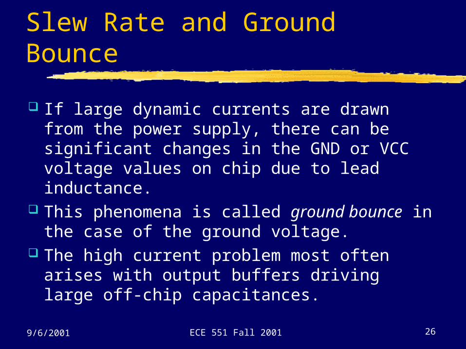
Slew Rate and Ground Bounce
If large dynamic currents are drawn from the power supply, there can be significant changes in the GND or VCC voltage values on chip due to lead inductance.
This phenomena is called ground bounce in the case of the ground voltage.
The high current problem most often arises with output buffers driving large off-chip capacitances.
ECE 551 Fall 2001 279/6/2001
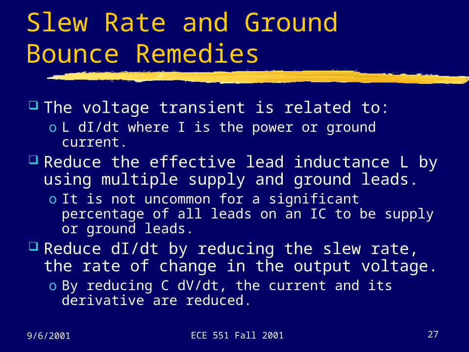
Slew Rate and Ground Bounce Remedies
The voltage transient is related to:o L dI/dt where I is the power or ground current.
Reduce the effective lead inductance L by using multiple supply and ground leads. o It is not uncommon for a significant percentage
of all leads on an IC to be supply or ground leads.
Reduce dI/dt by reducing the slew rate, the rate of change in the output voltage. o By reducing C dV/dt, the current and its
derivative are reduced.
ECE 551 Fall 2001 289/6/2001
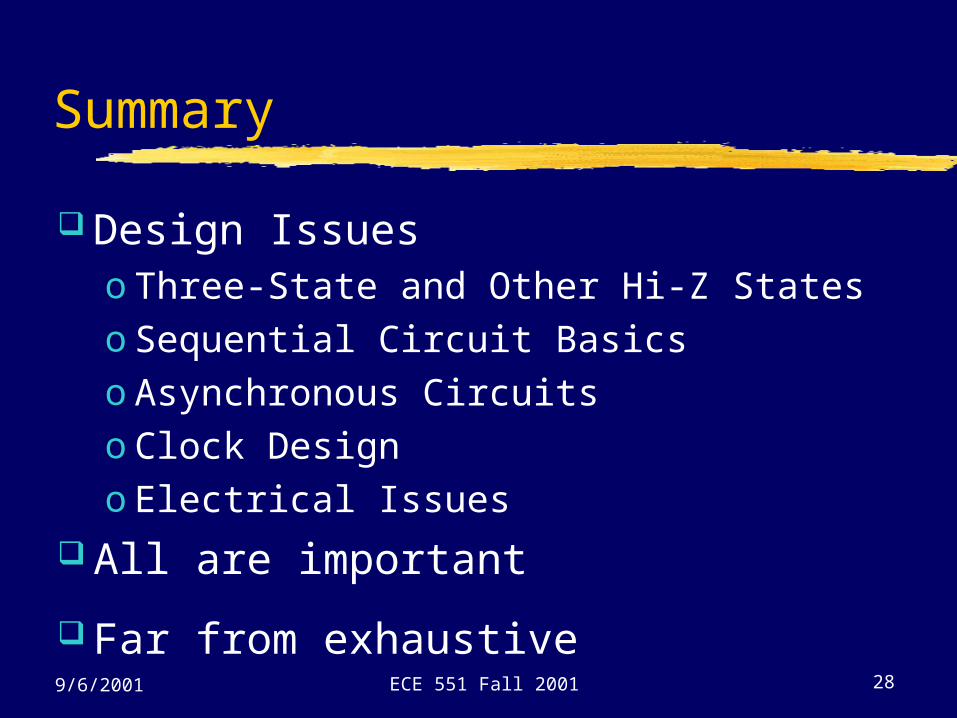
Summary
Design Issueso Three-State and Other Hi-Z Stateso Sequential Circuit Basicso Asynchronous Circuitso Clock Designo Electrical Issues
All are important
Far from exhaustive
ECE 551 Fall 2001 299/6/2001
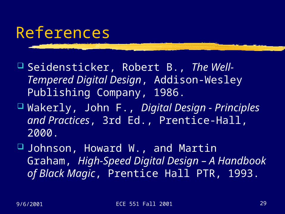
References
Seidensticker, Robert B., The Well-Tempered Digital Design, Addison-Wesley Publishing Company, 1986.
Wakerly, John F., Digital Design - Principles and Practices, 3rd Ed., Prentice-Hall, 2000.
Johnson, Howard W., and Martin Graham, High-Speed Digital Design – A Handbook of Black Magic, Prentice Hall PTR, 1993.