ece 448 – fpga and asic design with vhdl lecture 11 xilinx fpga memories
TRANSCRIPT
ECE 448 – FPGA and ASIC Design with VHDL
Lecture 11
Xilinx FPGA Memories
2ECE 448 – FPGA and ASIC Design with VHDL
Required reading
• P. Chu, FPGA Prototyping by VHDL Examples
Chapter 11, Xilinx Spartan-3 Specific Memory
3ECE 448 – FPGA and ASIC Design with VHDL
Recommended reading
• XAPP463 Using Block RAM in Spartan-3 Generation FPGAs
Google search: XAPP463
• XAPP464 Using Look-Up Tables as Distributed RAM in Spartan-3 Generation FPGAs
Google search: XAPP464
• XST User Guide, Section: RAMs and ROMs HDL Coding Techniques
Google search: XST User Guide (PDF)
• ISE In-Depth Tutorial, Section: Creating a CORE Generator Software Module
Google search: ISE In-Depth Tutorial

4
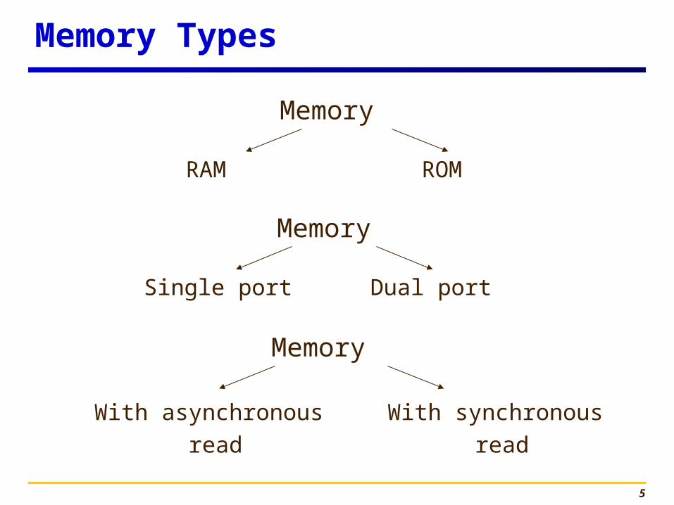
Memory Types
5
Memory Types
Memory
RAM ROM
Single port Dual port
With asynchronous
read
With synchronous
read
Memory
Memory
6
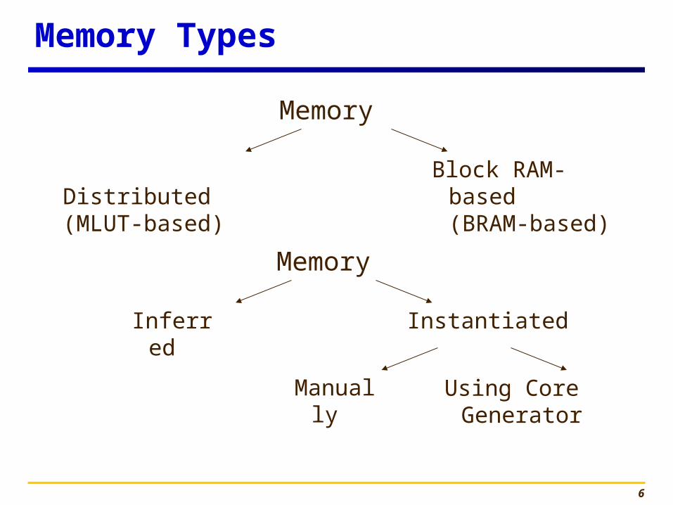
Memory Types
Memory
Distributed (MLUT-based)
Block RAM-based(BRAM-based)
Inferred Instantiated
Memory
Manually Using Core Generator

7
FPGA Distributed
Memory
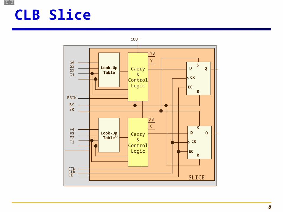
8
COUT
D Q
CK
S
REC
D Q
CK
REC
O
G4G3G2G1
Look-UpTable
Carry&
ControlLogic
O
YB
Y
F4F3F2F1
XB
X
Look-UpTable
F5IN
BYSR
S
Carry&
ControlLogic
CINCLKCE SLICE
CLB Slice
9
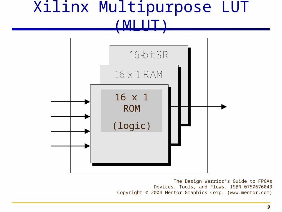
16-bit SR
16 x 1 RAM
4-input LUT
The Design Warrior’s Guide to FPGAsDevices, Tools, and Flows. ISBN 0750676043
Copyright © 2004 Mentor Graphics Corp. (www.mentor.com)
Xilinx Multipurpose LUT (MLUT)
16 x 1 ROM
(logic)
10
RAM16X1S
O
DWE
WCLKA0A1A2A3
RAM32X1S
O
DWEWCLKA0A1A2A3A4
RAM16X2S
O1
D0
WEWCLKA0A1A2A3
D1
O0
=
=LUT
LUT or
LUT
RAM16X1D
SPO
D
WE
WCLK
A0
A1
A2
A3
DPRA0 DPO
DPRA1
DPRA2
DPRA3
or
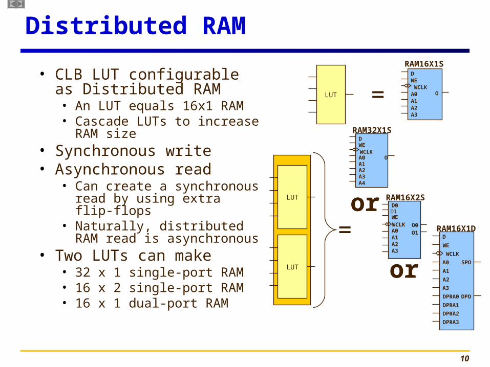
Distributed RAM
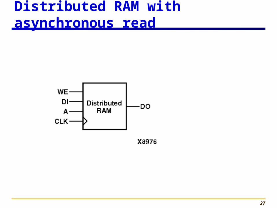
• CLB LUT configurable as Distributed RAM• An LUT equals 16x1 RAM• Cascade LUTs to increase RAM size
• Synchronous write• Asynchronous read
• Can create a synchronous read by using extra flip-flops
• Naturally, distributed RAM read is asynchronous
• Two LUTs can make• 32 x 1 single-port RAM• 16 x 2 single-port RAM• 16 x 1 dual-port RAM

11
FPGA Block RAM
12
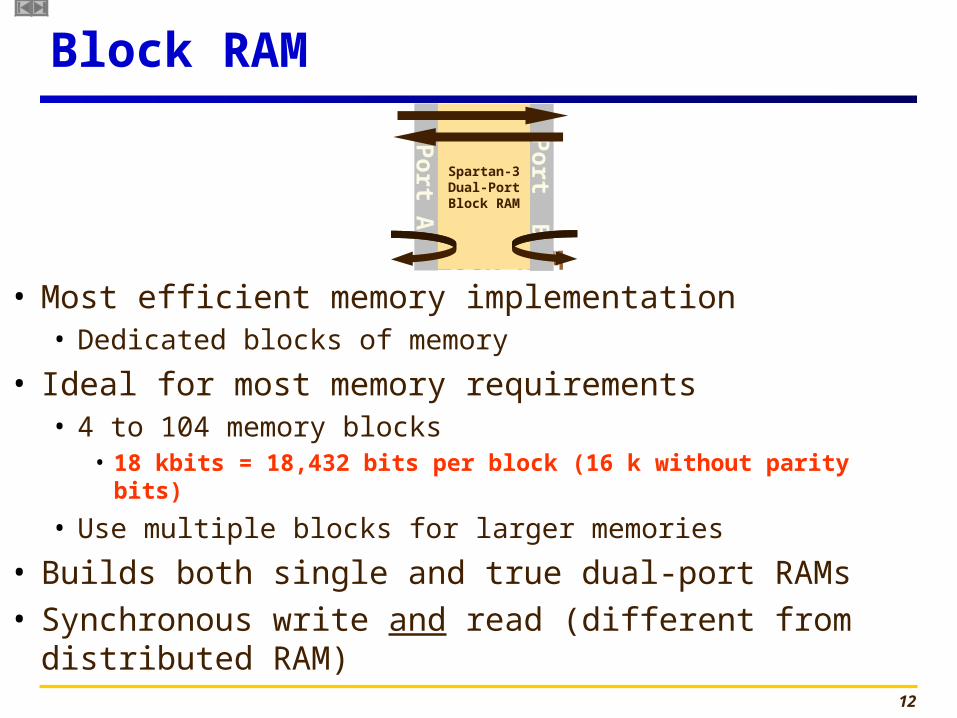
Block RAM
Spartan-3Dual-Port
Block RAM
Port A
Port B
Block RAM
• Most efficient memory implementation• Dedicated blocks of memory
• Ideal for most memory requirements• 4 to 104 memory blocks
• 18 kbits = 18,432 bits per block (16 k without parity bits)
• Use multiple blocks for larger memories• Builds both single and true dual-port RAMs• Synchronous write and read (different from distributed RAM)
13
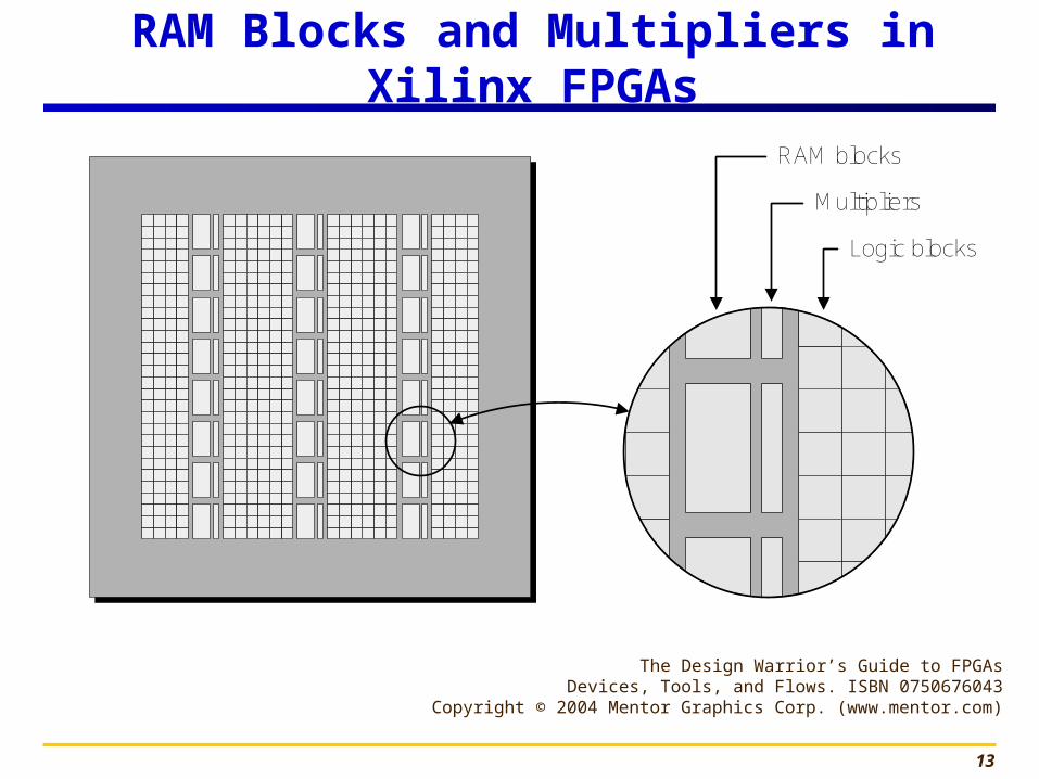
RAM blocks
Multipliers
Logic blocks
RAM Blocks and Multipliers in Xilinx FPGAs
The Design Warrior’s Guide to FPGAsDevices, Tools, and Flows. ISBN 0750676043
Copyright © 2004 Mentor Graphics Corp. (www.mentor.com)
14
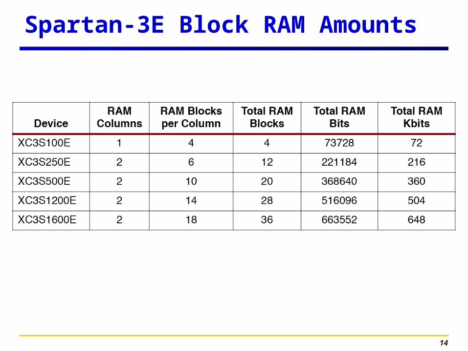
Spartan-3E Block RAM Amounts
15
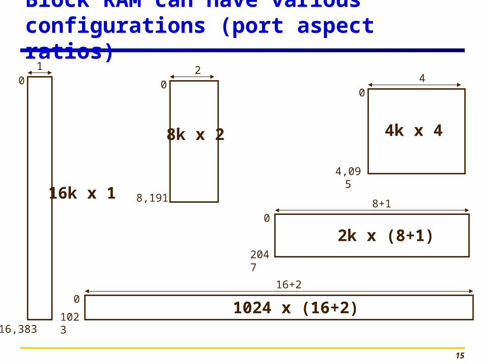
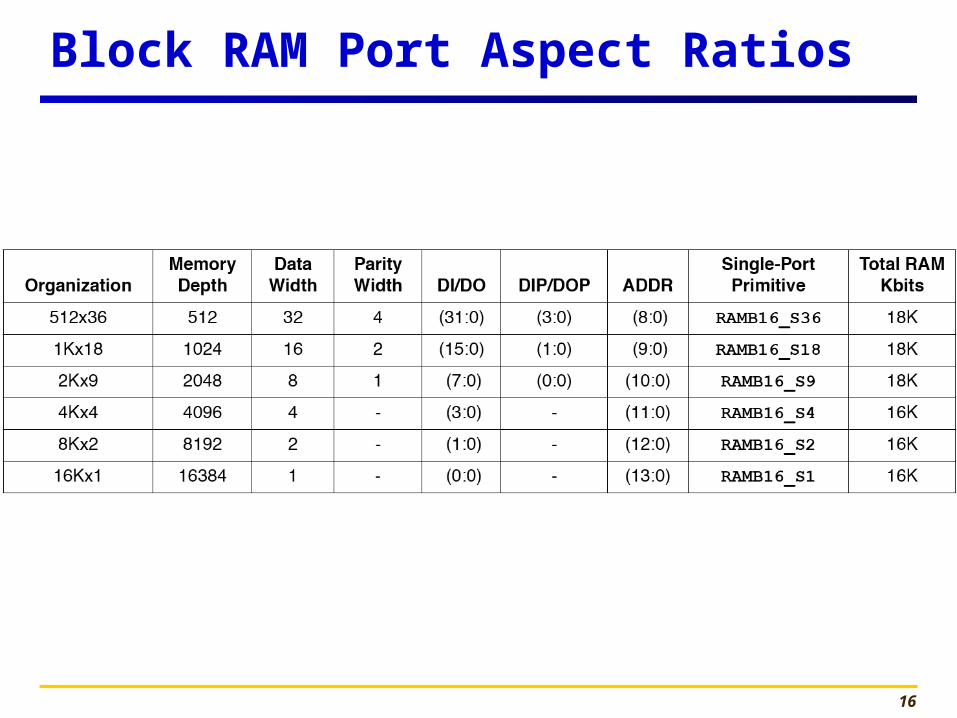
Block RAM can have various configurations (port aspect ratios)
0
16,383
1
4,095
40
8,191
20
2047
8+10
1023
16+20
16k x 1
8k x 2 4k x 4
2k x (8+1)
1024 x (16+2)
16
Block RAM Port Aspect Ratios
17
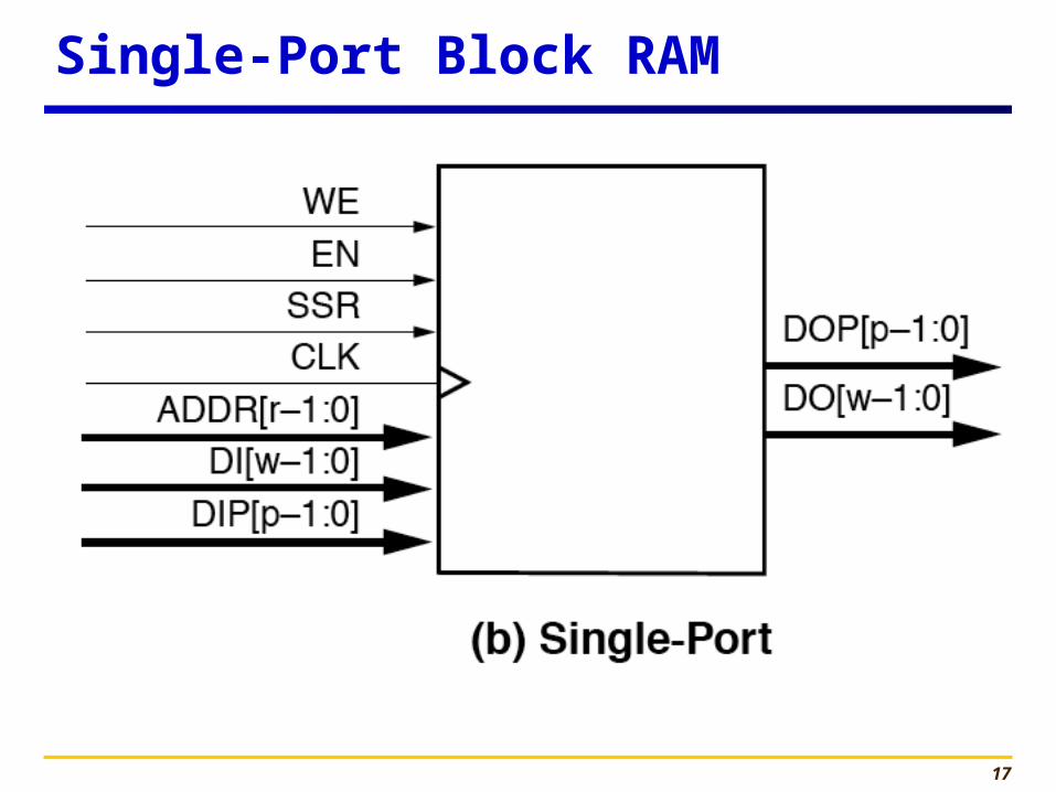
Single-Port Block RAM
18
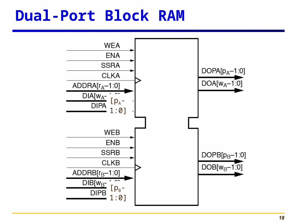
Dual-Port Block RAM
[pA-1:0]
[pB-1:0]

19
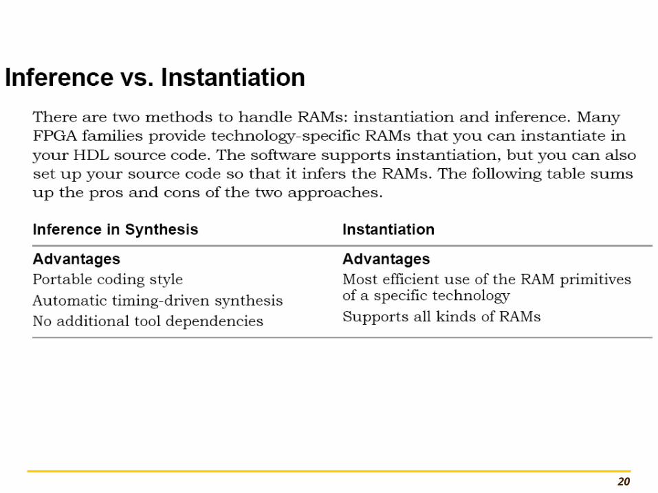
Inference vs.
Instantiation
20
21
Generic
Inferred
ROM
22
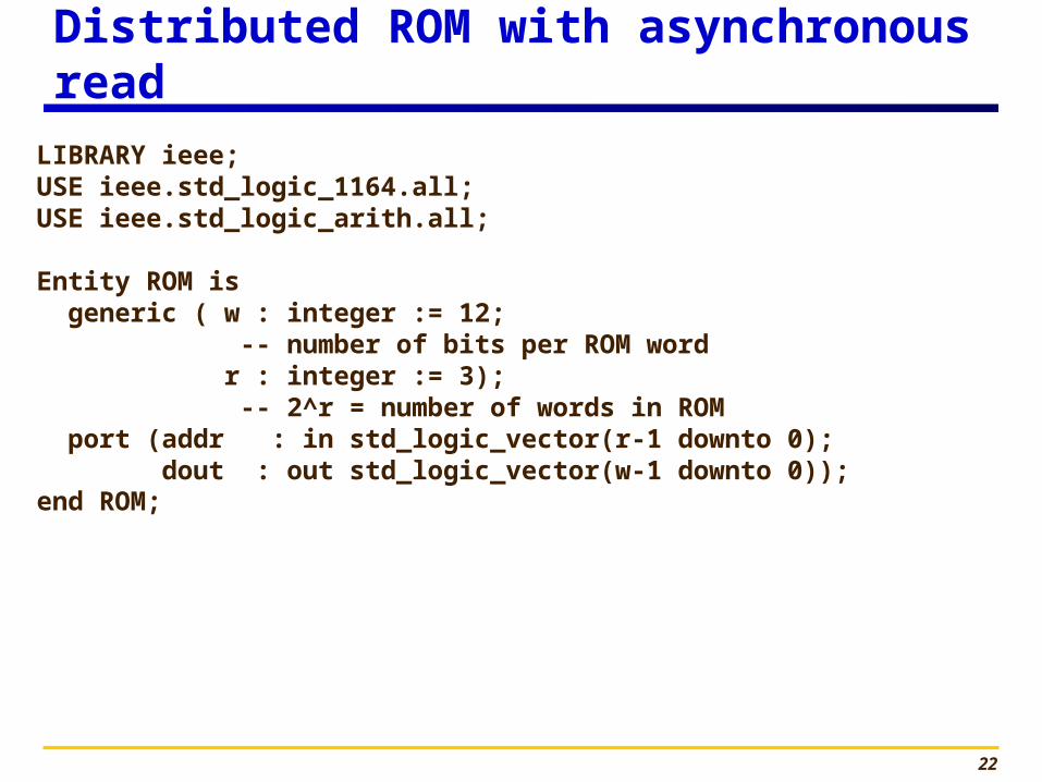
Distributed ROM with asynchronous read
LIBRARY ieee;USE ieee.std_logic_1164.all;USE ieee.std_logic_arith.all; Entity ROM is generic ( w : integer := 12; -- number of bits per ROM word r : integer := 3); -- 2^r = number of words in ROM port (addr : in std_logic_vector(r-1 downto 0); dout : out std_logic_vector(w-1 downto 0)); end ROM;
23
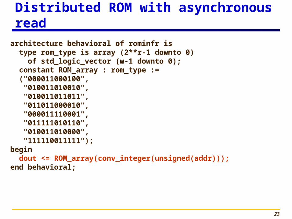
Distributed ROM with asynchronous read
architecture behavioral of rominfr is type rom_type is array (2**r-1 downto 0) of std_logic_vector (w-1 downto 0); constant ROM_array : rom_type := ("000011000100", "010011010010", "010011011011", "011011000010", "000011110001", "011111010110", "010011010000", "111110011111"); begin dout <= ROM_array(conv_integer(unsigned(addr))); end behavioral;
24
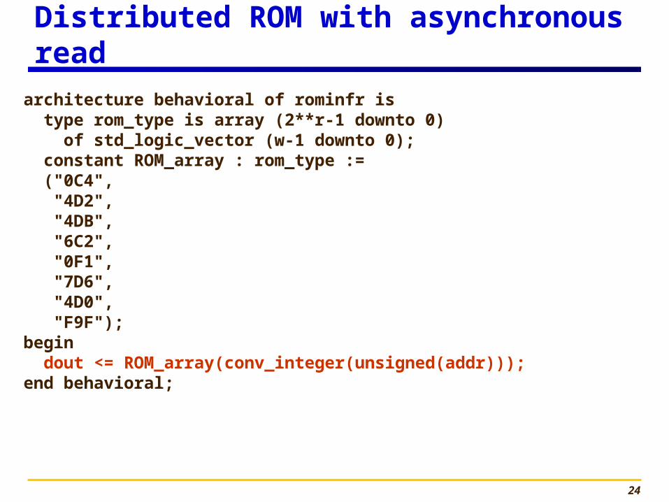
Distributed ROM with asynchronous read
architecture behavioral of rominfr is type rom_type is array (2**r-1 downto 0) of std_logic_vector (w-1 downto 0); constant ROM_array : rom_type := ("0C4", "4D2", "4DB", "6C2", "0F1", "7D6", "4D0", "F9F"); begin dout <= ROM_array(conv_integer(unsigned(addr))); end behavioral;

25
Generic
Inferred
RAM
26
Distributed versus Block RAM Inference
Examples:1. Distributed single-port RAM with asynchronous read
2. Distributed dual-port RAM with asynchronous read
1. Single-port Block RAM with synchronous read (no version with asynchronous read!)
More RAM coding examples in the XST Coding Guidelines.
27
Distributed RAM with asynchronous read
28
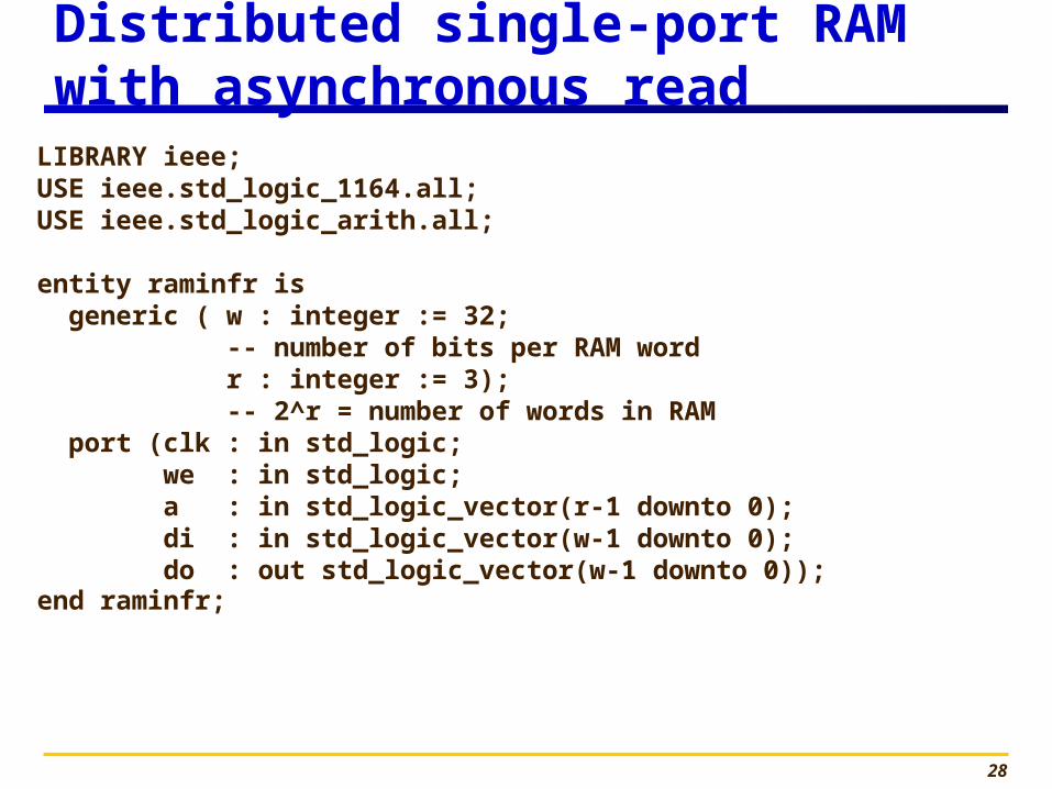
Distributed single-port RAM with asynchronous read
LIBRARY ieee;USE ieee.std_logic_1164.all;USE ieee.std_logic_arith.all; entity raminfr is generic ( w : integer := 32; -- number of bits per RAM word r : integer := 3); -- 2^r = number of words in RAM port (clk : in std_logic; we : in std_logic; a : in std_logic_vector(r-1 downto 0); di : in std_logic_vector(w-1 downto 0); do : out std_logic_vector(w-1 downto 0)); end raminfr;
29
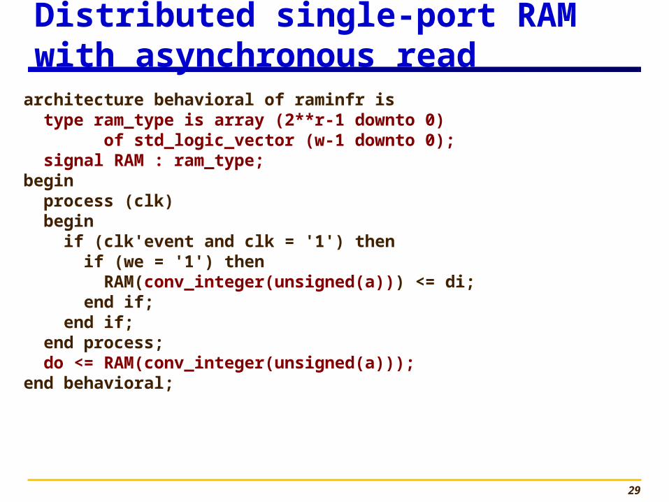
Distributed single-port RAM with asynchronous read
architecture behavioral of raminfr is type ram_type is array (2**r-1 downto 0) of std_logic_vector (w-1 downto 0); signal RAM : ram_type; begin process (clk) begin if (clk'event and clk = '1') then if (we = '1') then RAM(conv_integer(unsigned(a))) <= di; end if; end if; end process; do <= RAM(conv_integer(unsigned(a))); end behavioral;
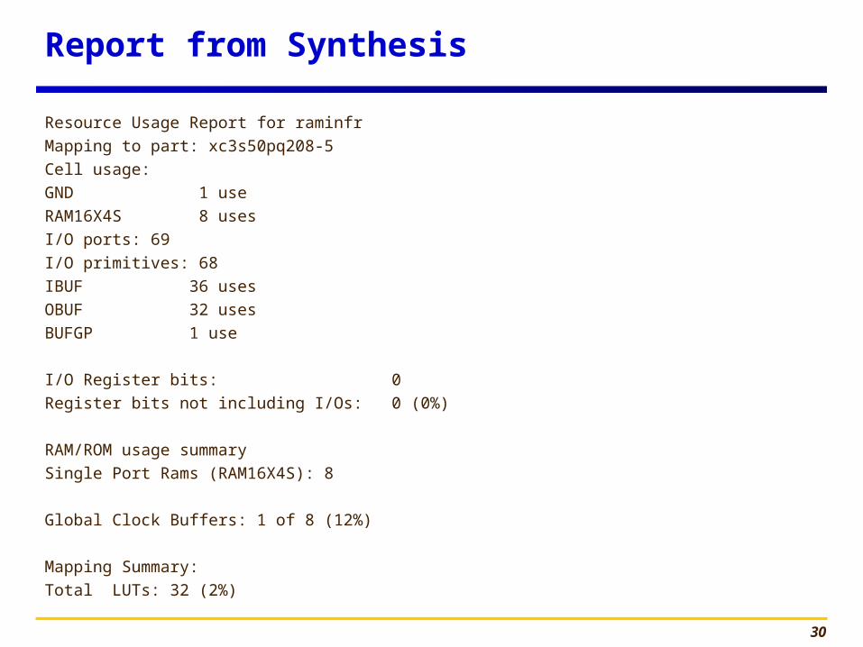
30
Report from Synthesis
Resource Usage Report for raminfr Mapping to part: xc3s50pq208-5Cell usage:GND 1 useRAM16X4S 8 usesI/O ports: 69I/O primitives: 68IBUF 36 usesOBUF 32 usesBUFGP 1 use
I/O Register bits: 0Register bits not including I/Os: 0 (0%)
RAM/ROM usage summarySingle Port Rams (RAM16X4S): 8
Global Clock Buffers: 1 of 8 (12%)
Mapping Summary:Total LUTs: 32 (2%)
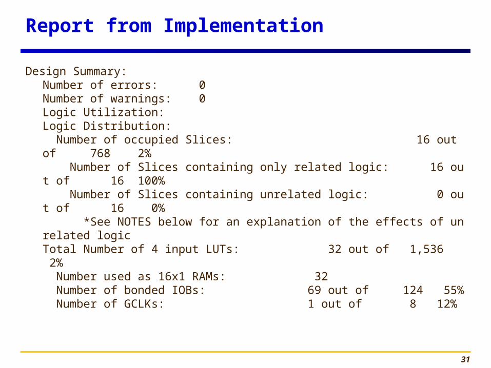
31
Report from Implementation
Design Summary:Number of errors: 0Number of warnings: 0Logic Utilization:Logic Distribution: Number of occupied Slices: 16 out of 768 2% Number of Slices containing only related logic: 16 out of 16 100% Number of Slices containing unrelated logic: 0 out of 16 0% *See NOTES below for an explanation of the effects of unrelated logicTotal Number of 4 input LUTs: 32 out of 1,536 2% Number used as 16x1 RAMs: 32 Number of bonded IOBs: 69 out of 124 55% Number of GCLKs: 1 out of 8 12%
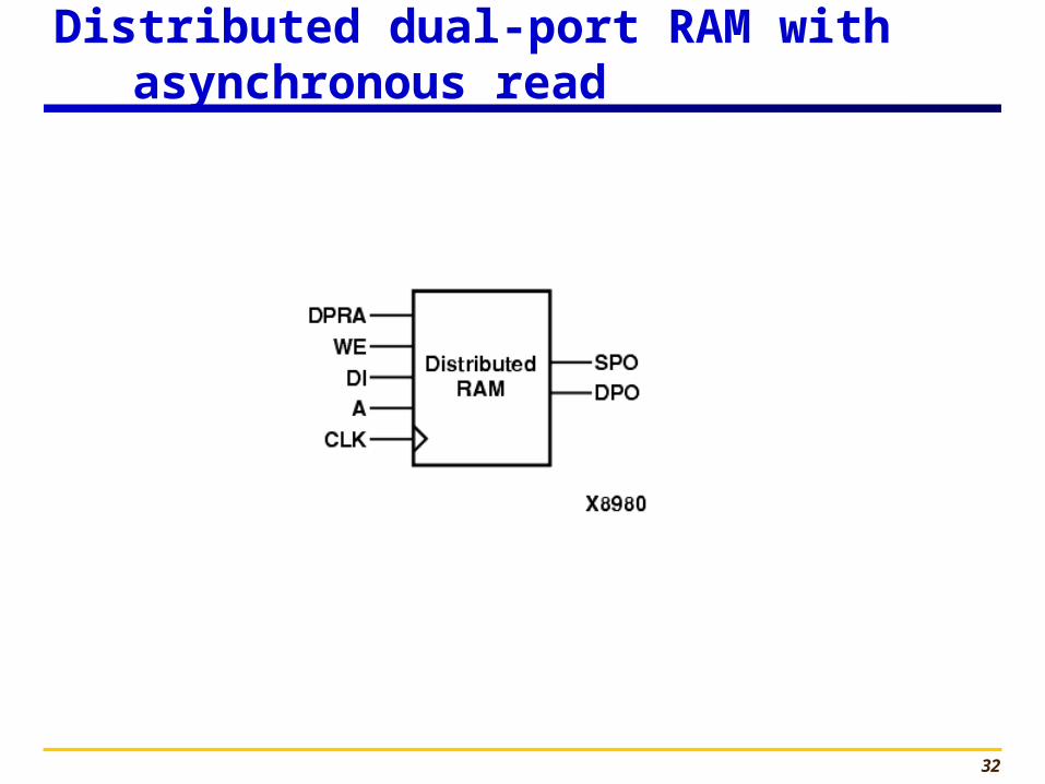
32
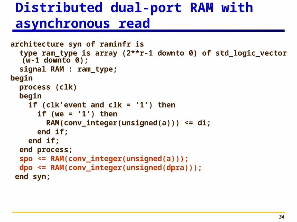
Distributed dual-port RAM with asynchronous read
33
Distributed dual-port RAM with asynchronous read
library ieee; use ieee.std_logic_1164.all; use ieee.std_logic_unsigned.all; use ieee.std_logic_arith.all; entity raminfr is generic ( w : integer := 32; -- number of bits per RAM word r : integer := 3); -- 2^r = number of words in RAM port (clk : in std_logic; we : in std_logic; a : in std_logic_vector(r-1 downto 0); dpra : in std_logic_vector(r-1 downto 0); di : in std_logic_vector(w-1 downto 0); spo : out std_logic_vector(w-1 downto 0); dpo : out std_logic_vector(w-1 downto 0)); end raminfr;
34
Distributed dual-port RAM with asynchronous read
architecture syn of raminfr is type ram_type is array (2**r-1 downto 0) of std_logic_vector
(w-1 downto 0); signal RAM : ram_type; begin process (clk) begin if (clk'event and clk = '1') then if (we = '1') then RAM(conv_integer(unsigned(a))) <= di; end if; end if; end process; spo <= RAM(conv_integer(unsigned(a))); dpo <= RAM(conv_integer(unsigned(dpra))); end syn;
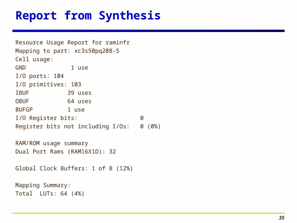
35
Report from Synthesis
Resource Usage Report for raminfr Mapping to part: xc3s50pq208-5Cell usage:GND 1 useI/O ports: 104I/O primitives: 103IBUF 39 usesOBUF 64 usesBUFGP 1 useI/O Register bits: 0Register bits not including I/Os: 0 (0%)
RAM/ROM usage summaryDual Port Rams (RAM16X1D): 32
Global Clock Buffers: 1 of 8 (12%)
Mapping Summary:Total LUTs: 64 (4%)
36
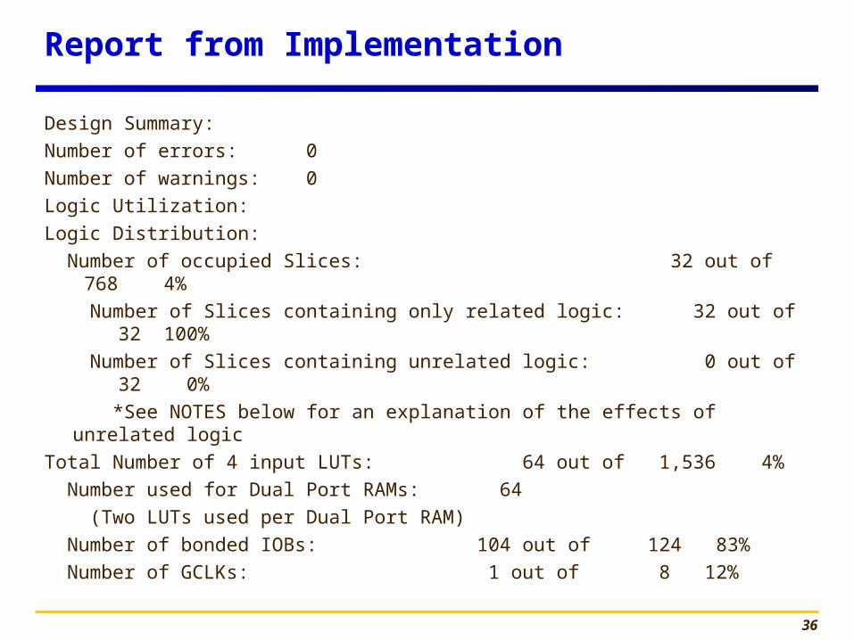
Report from Implementation
Design Summary:Number of errors: 0Number of warnings: 0Logic Utilization:Logic Distribution: Number of occupied Slices: 32 out of 768 4% Number of Slices containing only related logic: 32 out of 32 100% Number of Slices containing unrelated logic: 0 out of 32 0% *See NOTES below for an explanation of the effects of unrelated logicTotal Number of 4 input LUTs: 64 out of 1,536 4% Number used for Dual Port RAMs: 64 (Two LUTs used per Dual Port RAM) Number of bonded IOBs: 104 out of 124 83% Number of GCLKs: 1 out of 8 12%
37
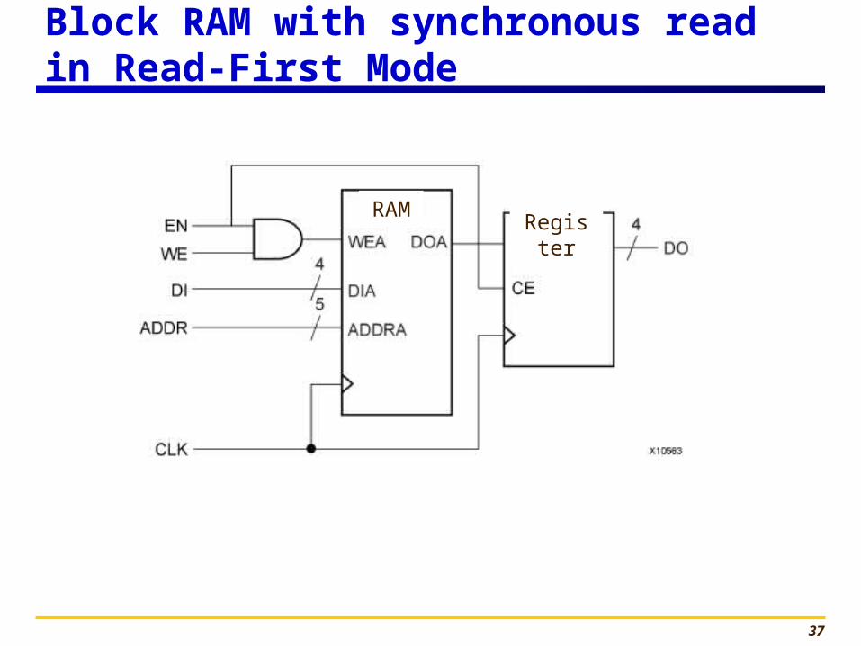
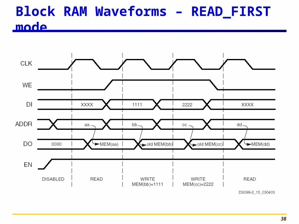
Block RAM with synchronous readin Read-First Mode
RAMRegister
38
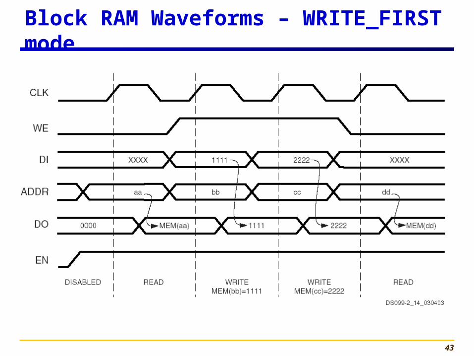
Block RAM Waveforms – READ_FIRST mode

39
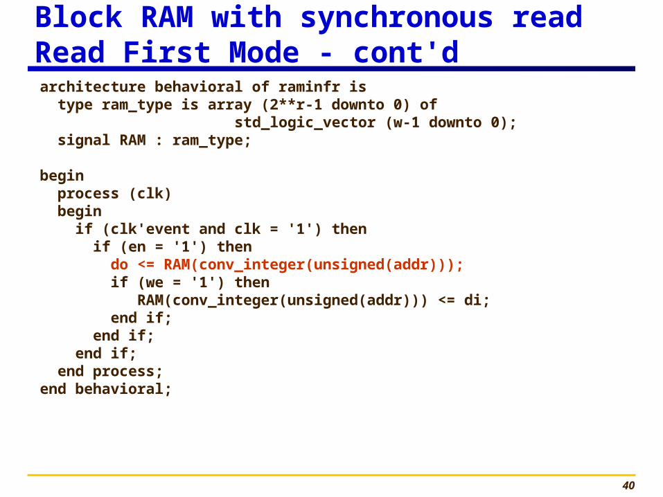
Block RAM with synchronous read Read-First Mode
LIBRARY ieee;USE ieee.std_logic_1164.all;USE ieee.std_logic_arith.all; entity raminfr is generic ( w : integer := 32; -- number of bits per RAM word r : integer := 9); -- 2^r = number of words in RAM port (clk : in std_logic; we : in std_logic; en : in std_logic; addr : in std_logic_vector(r-1 downto 0); di : in std_logic_vector(w-1 downto 0); do : out std_logic_vector(w-1 downto 0)); end raminfr;
40
Block RAM with synchronous read Read First Mode - cont'darchitecture behavioral of raminfr is type ram_type is array (2**r-1 downto 0) of std_logic_vector (w-1 downto 0); signal RAM : ram_type;
begin process (clk) begin if (clk'event and clk = '1') then if (en = '1') then do <= RAM(conv_integer(unsigned(addr))); if (we = '1') then RAM(conv_integer(unsigned(addr))) <= di; end if; end if; end if; end process; end behavioral;
41
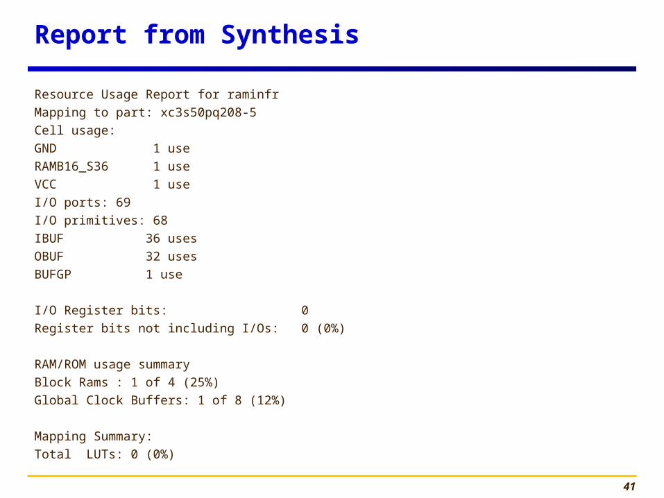
Report from Synthesis
Resource Usage Report for raminfr Mapping to part: xc3s50pq208-5Cell usage:GND 1 useRAMB16_S36 1 useVCC 1 useI/O ports: 69I/O primitives: 68IBUF 36 usesOBUF 32 usesBUFGP 1 use
I/O Register bits: 0Register bits not including I/Os: 0 (0%)
RAM/ROM usage summaryBlock Rams : 1 of 4 (25%)Global Clock Buffers: 1 of 8 (12%)
Mapping Summary:Total LUTs: 0 (0%)
42
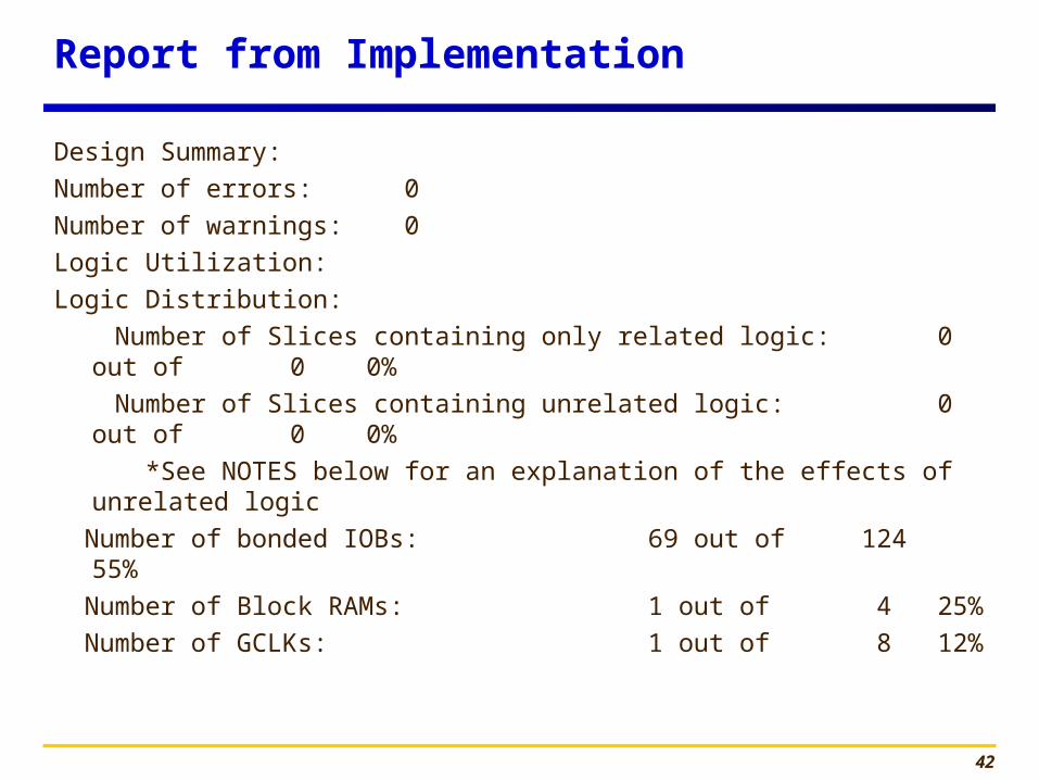
Report from Implementation
Design Summary:Number of errors: 0Number of warnings: 0Logic Utilization:Logic Distribution: Number of Slices containing only related logic: 0 out of 0 0% Number of Slices containing unrelated logic: 0 out of 0 0% *See NOTES below for an explanation of the effects of unrelated logic Number of bonded IOBs: 69 out of 124 55% Number of Block RAMs: 1 out of 4 25% Number of GCLKs: 1 out of 8 12%
43
Block RAM Waveforms – WRITE_FIRST mode
44
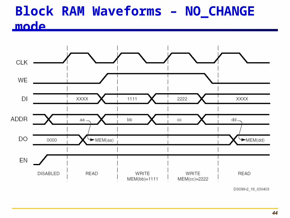
Block RAM Waveforms – NO_CHANGE mode

45
FPGA
specific memories:
Instantiation
46
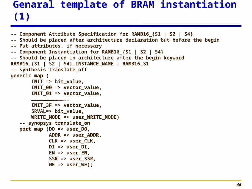
Genaral template of BRAM instantiation (1)
-- Component Attribute Specification for RAMB16_{S1 | S2 | S4} -- Should be placed after architecture declaration but before the begin-- Put attributes, if necessary -- Component Instantiation for RAMB16_{S1 | S2 | S4} -- Should be placed in architecture after the begin keyword RAMB16_{S1 | S2 | S4}_INSTANCE_NAME : RAMB16_S1 -- synthesis translate_off generic map ( INIT => bit_value, INIT_00 => vector_value, INIT_01 => vector_value, …………………………….. INIT_3F => vector_value, SRVAL=> bit_value, WRITE_MODE => user_WRITE_MODE) -- synopsys translate_on port map (DO => user_DO, ADDR => user_ADDR, CLK => user_CLK, DI => user_DI, EN => user_EN, SSR => user_SSR, WE => user_WE);
47
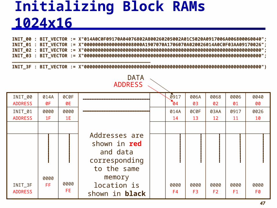
INIT_00 : BIT_VECTOR := X"014A0C0F09170A04076802A800260205002A01C5020A0917006A006800060040";INIT_01 : BIT_VECTOR := X"000000000000000008000A1907070A1706070A020026014A0C0F03AA09170026";INIT_02 : BIT_VECTOR := X"0000000000000000000000000000000000000000000000000000000000000000";INIT_03 : BIT_VECTOR := X"0000000000000000000000000000000000000000000000000000000000000000";……………………………………………………………………………………………………………………………………INIT_3F : BIT_VECTOR := X"0000000000000000000000000000000000000000000000000000000000000000")
0000F0
0000F1
0000F2
0000F3
0000F4
0000FE
0000FFINIT_3F
ADDRESS
002610
091711
03AA12
0C0F13
014A14
00001E
00001F
INIT_01ADDRESS
004000
000601
006802
006A03
091704
0C0F0E
014A0F
INIT_00ADDRESS
Addresses are shown in red and
data corresponding to the same
memory location is shown in black
ADDRESSDATA
Initializing Block RAMs 1024x16
48
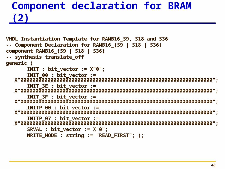
Component declaration for BRAM (2)
VHDL Instantiation Template for RAMB16_S9, S18 and S36 -- Component Declaration for RAMB16_{S9 | S18 | S36} component RAMB16_{S9 | S18 | S36} -- synthesis translate_off generic ( INIT : bit_vector := X"0"; INIT_00 : bit_vector :=
X"0000000000000000000000000000000000000000000000000000000000000000"; INIT_3E : bit_vector :=
X"0000000000000000000000000000000000000000000000000000000000000000"; INIT_3F : bit_vector :=
X"0000000000000000000000000000000000000000000000000000000000000000"; INITP_00 : bit_vector :=
X"0000000000000000000000000000000000000000000000000000000000000000"; INITP_07 : bit_vector :=
X"0000000000000000000000000000000000000000000000000000000000000000"; SRVAL : bit_vector := X"0"; WRITE_MODE : string := "READ_FIRST"; );
49
Component declaration for BRAM (2)
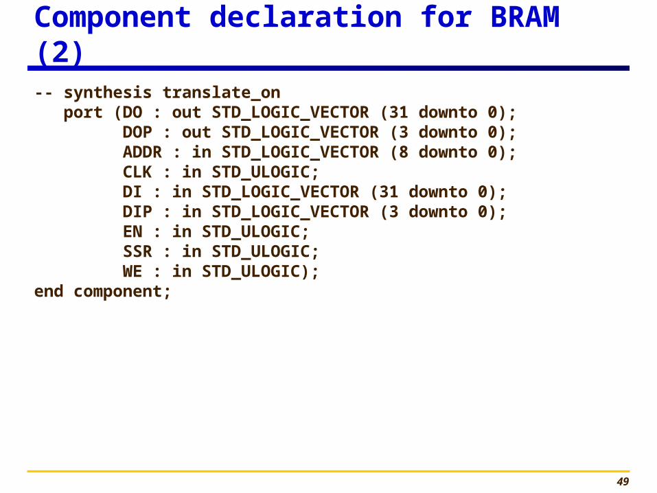
-- synthesis translate_on port (DO : out STD_LOGIC_VECTOR (31 downto 0); DOP : out STD_LOGIC_VECTOR (3 downto 0); ADDR : in STD_LOGIC_VECTOR (8 downto 0); CLK : in STD_ULOGIC; DI : in STD_LOGIC_VECTOR (31 downto 0); DIP : in STD_LOGIC_VECTOR (3 downto 0); EN : in STD_ULOGIC; SSR : in STD_ULOGIC; WE : in STD_ULOGIC); end component;
50
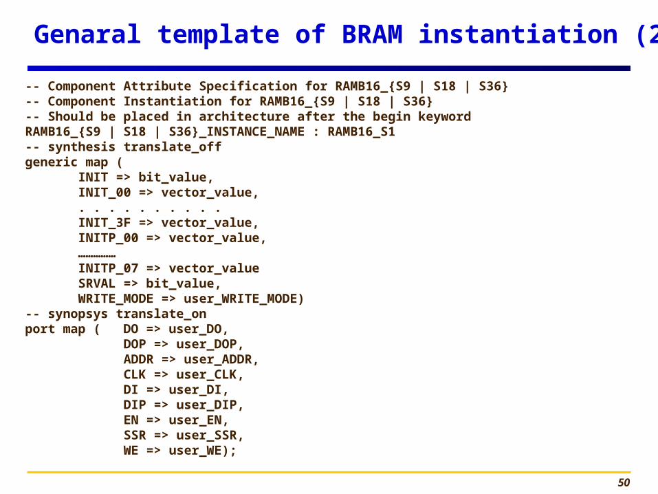
-- Component Attribute Specification for RAMB16_{S9 | S18 | S36} -- Component Instantiation for RAMB16_{S9 | S18 | S36} -- Should be placed in architecture after the begin keyword RAMB16_{S9 | S18 | S36}_INSTANCE_NAME : RAMB16_S1 -- synthesis translate_off generic map ( INIT => bit_value, INIT_00 => vector_value, . . . . . . . . . . INIT_3F => vector_value, INITP_00 => vector_value, …………… INITP_07 => vector_value SRVAL => bit_value, WRITE_MODE => user_WRITE_MODE) -- synopsys translate_on port map ( DO => user_DO, DOP => user_DOP, ADDR => user_ADDR, CLK => user_CLK, DI => user_DI, DIP => user_DIP, EN => user_EN, SSR => user_SSR, WE => user_WE);
Genaral template of BRAM instantiation (2)

51
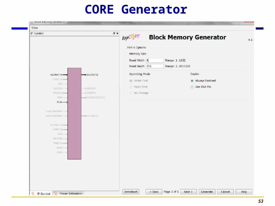
Using
CORE
Generator
52
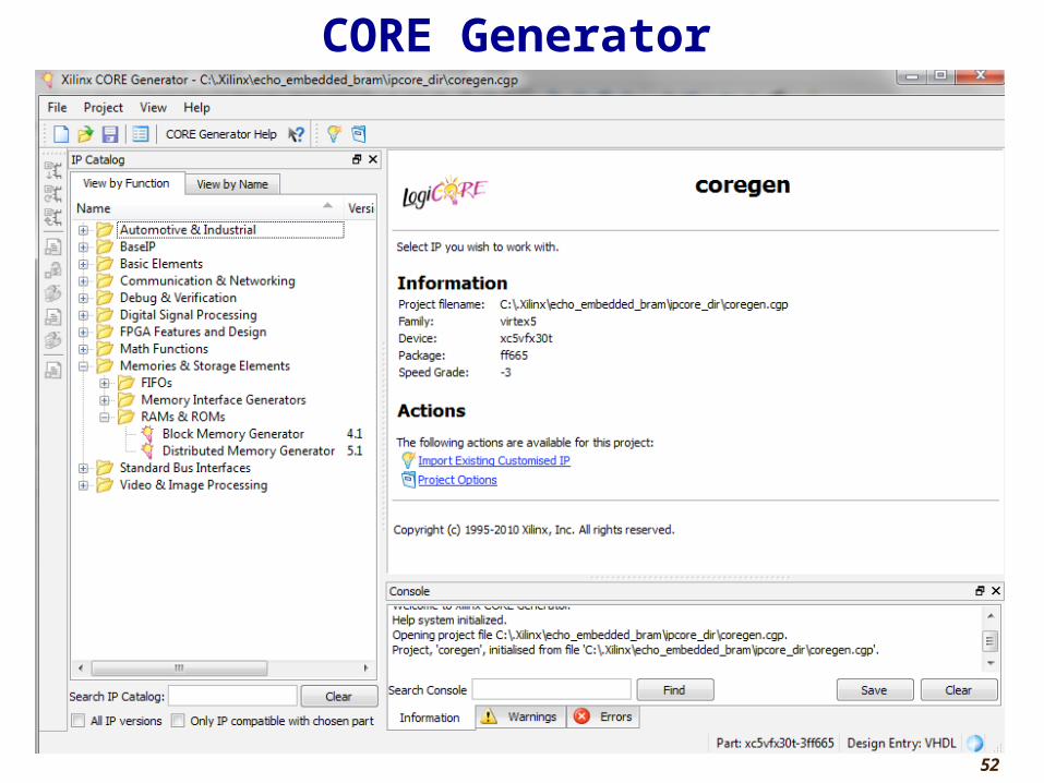
CORE Generator
53
CORE Generator