ec406pc: analog and digital communications lab … · experiment no:1 amplitude modulation and...
TRANSCRIPT
EC406PC: ANALOG AND DIGITAL COMMUNICATIONS LAB
B.Tech. II Year II Sem. L T P C
0 0 3 1.5
Note:
Minimum 12 experiments should be conducted:
All these experiments are to be simulated first either using MATLAB, COMSIM or any
other simulation package and then to be realized in hardware
List of Experiments:
1. (i) Amplitude modulation and demodulation (ii) Spectrum analysis of AM
2. (i) Frequency modulation and demodulation (ii) Spectrum analysis of FM
3. DSB-SC Modulator & Detector
4. SSB-SC Modulator & Detector (Phase Shift Method)
5. Frequency Division Multiplexing & De multiplexing
6. Pulse Amplitude Modulation & Demodulation
7. Pulse Width Modulation & Demodulation
8. Pulse Position Modulation & Demodulation
9. PCM Generation and Detection
10. Delta Modulation
11. Frequency Shift Keying: Generation and Detection
12. Binary Phase Shift Keying: Generation and Detection
13. Generation and Detection (i) DPSK (ii) QPSK
Major Equipments required for Laboratories:
1. CROs: 20MHz
2. Function Generators: 2MHz
3. Spectrum Analyzer
4. Regulated Power Supplies: 0-30V
5. MAT Lab/Equivalent Simulation Package with Communication tool box
6. Analog and Digital Modulation and Demodulation Trainer Kits.
S.NO
NAME OF THE EXPERIMENT
PAGE NO
1 (i) Amplitude modulation and demodulation
(ii) Spectrum analysis of AM
2 (i) Frequency modulation and demodulation
(ii) Spectrum analysis of FM
3 DSB-SC Modulator & Detector
4
SSB-SC Modulator & Detector (Phase Shift Method)
5 Frequency Division Multiplexing & De multiplexing
6 Pulse Amplitude Modulation & Demodulation
7
Pulse Width Modulation & Demodulation
8 Pulse Position Modulation & Demodulation
9 PCM Generation and Detection
10 Delta Modulation
11
Frequency Shift Keying: Generation and Detection
12
Binary Phase Shift Keying: Generation and Detection
13 Generation and Detection (i) DPSK (ii) QPSK
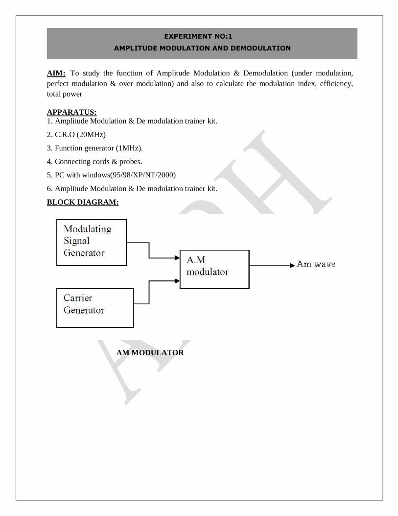
EXPERIMENT NO:1
AMPLITUDE MODULATION AND DEMODULATION
AIM: To study the function of Amplitude Modulation & Demodulation (under modulation,
perfect modulation & over modulation) and also to calculate the modulation index, efficiency,
total power
APPARATUS:
1. Amplitude Modulation & De modulation trainer kit.
2. C.R.O (20MHz)
3. Function generator (1MHz).
4. Connecting cords & probes.
5. PC with windows(95/98/XP/NT/2000)
6. Amplitude Modulation & De modulation trainer kit.
BLOCK DIAGRAM:
AM MODULATOR
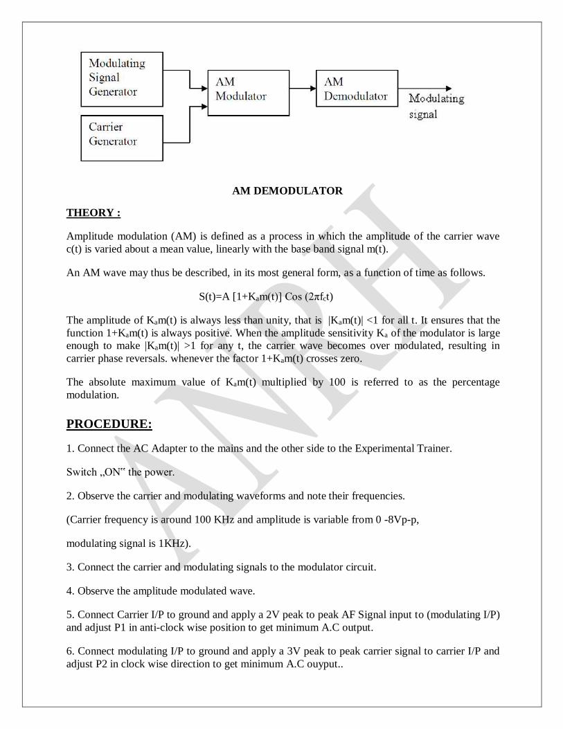
AM DEMODULATOR
THEORY :
Amplitude modulation (AM) is defined as a process in which the amplitude of the carrier wave
c(t) is varied about a mean value, linearly with the base band signal m(t).
An AM wave may thus be described, in its most general form, as a function of time as follows.
S(t)=A [1+Kam(t)] Cos (2πfct)
The amplitude of Kam(t) is always less than unity, that is |Kam(t)| <1 for all t. It ensures that the
function 1+Kam(t) is always positive. When the amplitude sensitivity Ka of the modulator is large
enough to make |Kam(t)| >1 for any t, the carrier wave becomes over modulated, resulting in
carrier phase reversals. whenever the factor 1+Kam(t) crosses zero.
The absolute maximum value of Kam(t) multiplied by 100 is referred to as the percentage
modulation.
PROCEDURE:
1. Connect the AC Adapter to the mains and the other side to the Experimental Trainer.
Switch „ON‟ the power.
2. Observe the carrier and modulating waveforms and note their frequencies.
(Carrier frequency is around 100 KHz and amplitude is variable from 0 -8Vp-p,
modulating signal is 1KHz).
3. Connect the carrier and modulating signals to the modulator circuit.
4. Observe the amplitude modulated wave.
5. Connect Carrier I/P to ground and apply a 2V peak to peak AF Signal input to (modulating I/P)
and adjust P1 in anti-clock wise position to get minimum A.C output.
6. Connect modulating I/P to ground and apply a 3V peak to peak carrier signal to carrier I/P and
adjust P2 in clock wise direction to get minimum A.C ouyput..
7. Connect modulating input &carrier input to ground and adjust P3 for zero D.C output.
8. Make modulating i/p 2 Vpp and carrier i/p 3 Vpp peak to peak and adjust potentiometer P4 for
maximum output.
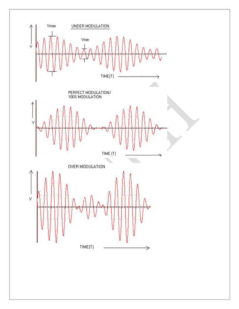
9. Calculate maximum and minimum points on the modulated envelope on a CRO and calculate
the depth of modulation.
10. Observe that by varying the modulating voltage, the depth of modulation varies.
11. During demodulation connect this AM output to the input of the demodulator.
12. By adjusting the RC time constant (i.e., cut off frequency) of the filter circuit we get
minimum distorted output.
13. Observe that this demodulated output is amplified has some phase delay because of RC
components.
14. Also observe the effects by changing the carrier amplitudes.
15. In all cases, calculate the modulation index.
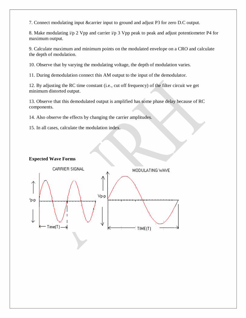
Expected Wave Forms
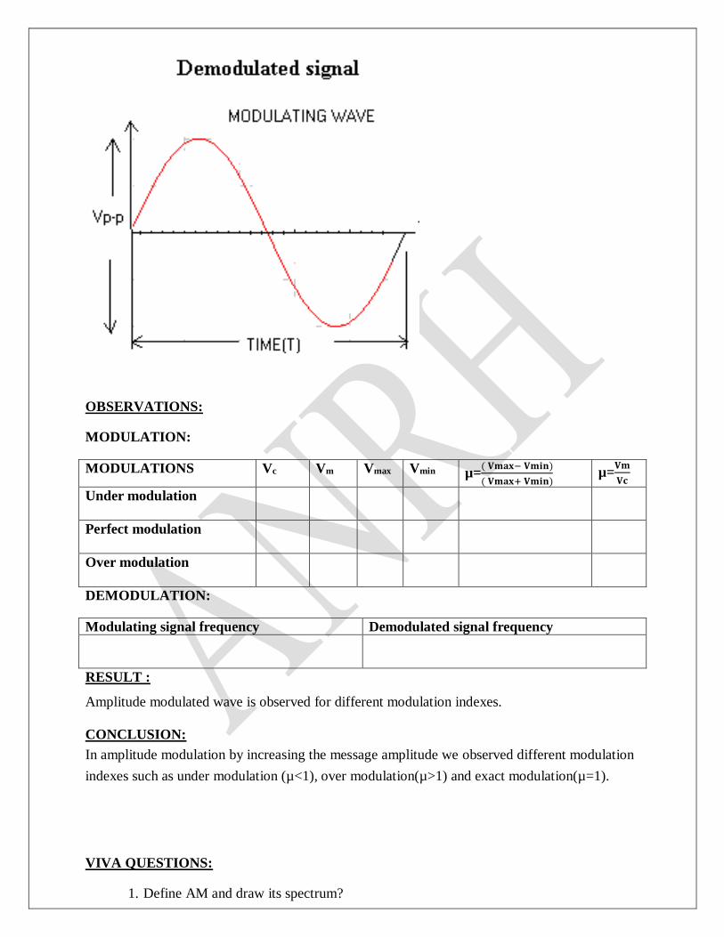
OBSERVATIONS:
MODULATION:
MODULATIONS Vc Vm Vmax Vmin µ=( 𝐕𝐦𝐚𝐱− 𝐕𝐦𝐢𝐧)
( 𝐕𝐦𝐚𝐱+ 𝐕𝐦𝐢𝐧) µ=
𝐕𝐦
𝐕𝐜
Under modulation
Perfect modulation
Over modulation
DEMODULATION:
Modulating signal frequency Demodulated signal frequency
RESULT : Amplitude modulated wave is observed for different modulation indexes.
CONCLUSION:
In amplitude modulation by increasing the message amplitude we observed different modulation
indexes such as under modulation (µ<1), over modulation(µ>1) and exact modulation(µ=1).
VIVA QUESTIONS:
1. Define AM and draw its spectrum?
2. Draw the phase’s representation of an amplitude modulated wave?
3. Give the significance of modulation index?
4. What are the different degrees of modulation?
5. What are the limitations of square law modulator?
Matlab code:
fs=8000; fm=20; fc=500; Am=1; Ac=1; t=[0:.1*fs]/fs; m=Am*cos(2*pi*fm*t); c=Ac*cos(2*pi*fc*t); ka=0.5; u=ka*Am; s1=Ac*(1+u*cos(2*pi*fm*t)).*cos(2*pi*fc*t); subplot(4,3,1:3); plot(t,m); title('Modulating or Message signal(fm=20Hz)'); subplot(4,3,4:6); plot(t,c); title('Carrier signal(fc=500Hz)'); subplot(4,3,7); plot(t,s1); title( 'Under Modulated signal(ka.Am=0.5)'); Am=2; ka=0.5; u=ka*Am; s2=Ac*(1+u*cos(2*pi*fm*t)).*cos(2*pi*fc*t); subplot(4,3,8); plot(t,s2); title( 'Exact Modulated signal(ka.Am=1)'); Am=5; ka=0.5; u=ka*Am; s3=Ac*(1+u*cos(2*pi*fm*t)).*cos(2*pi*fc*t); subplot(4,3,9); plot(t,s3); title('Over Modulated signal(ka.Am=2.5)'); r1= s1.*c; [b a] = butter(1,0.01); mr1= filter(b,a,r1); subplot(4,3,10); plot(t,mr1); r2= s2.*c; [b a] = butter(1,0.01); mr2= filter(b,a,r2); subplot(4,3,11); plot(t,mr2);
r3= s3.*c;
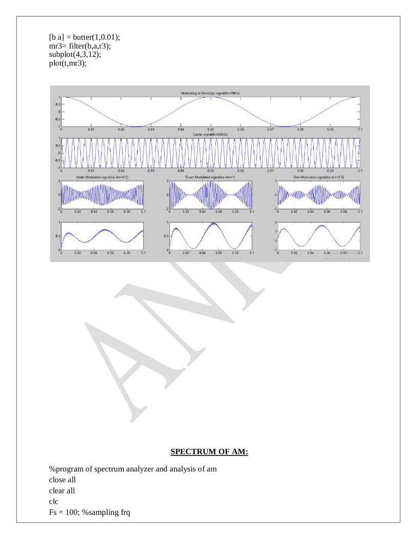
[b a] = butter(1,0.01); mr3= filter(b,a,r3); subplot(4,3,12); plot(t,mr3);
SPECTRUM OF AM:
%program of spectrum analyzer and analysis of am
close all
clear all
clc
Fs = 100; %sampling frq
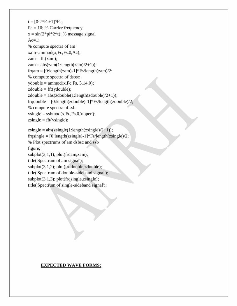
t = [0:2*Fs+1]'/Fs;
Fc = 10; % Carrier frequency
x = sin(2*pi*2*t); % message signal
Ac=1;
% compute spectra of am
xam=ammod(x,Fc,Fs,0,Ac);
zam = fft(xam);
zam = abs(zam(1:length(zam)/2+1));
frqam = [0:length(zam)-1]*Fs/length(zam)/2;
% compute spectra of dsbsc
ydouble = ammod(x,Fc,Fs, 3.14,0);
zdouble = fft(ydouble);
zdouble = abs(zdouble(1:length(zdouble)/2+1));
frqdouble = [0:length(zdouble)-1]*Fs/length(zdouble)/2;
% compute spectra of ssb
ysingle = ssbmod(x,Fc,Fs,0,'upper');
zsingle = fft(ysingle);
zsingle = abs(zsingle(1:length(zsingle)/2+1));
frqsingle = [0:length(zsingle)-1]*Fs/length(zsingle)/2;
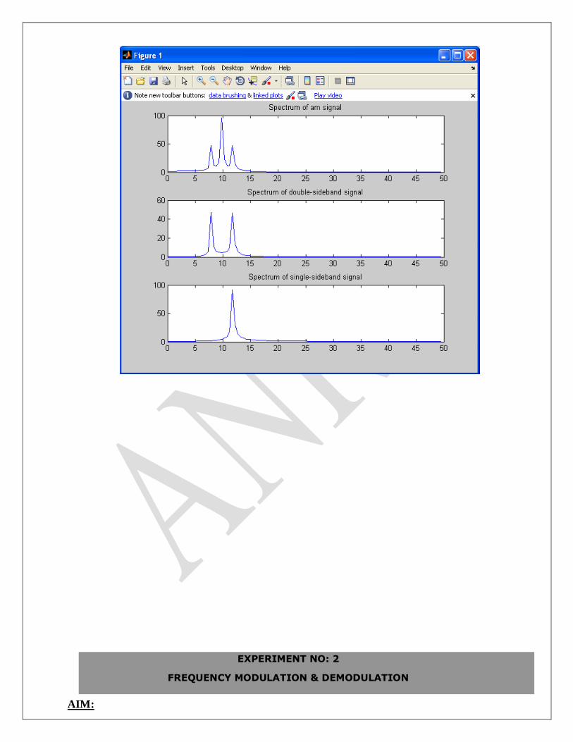
% Plot spectrums of am dsbsc and ssb
figure;
subplot(3,1,1); plot(frqam,zam);
title('Spectrum of am signal');
subplot(3,1,2); plot(frqdouble,zdouble);
title('Spectrum of double-sideband signal');
subplot(3,1,3); plot(frqsingle,zsingle);
title('Spectrum of single-sideband signal');
EXPECTED WAVE FORMS:
EXPERIMENT NO: 2
FREQUENCY MODULATION & DEMODULATION
AIM:
To study the functioning of frequency modulation & demodulation and to calculate the
modulation index.
APPARATUS:
1. Frequency modulation & demodulation trainer kit.
2. C.R.O (20MHz)
3. Function generator (1MHz).
4. Connecting chords & probes.
BLOCK DIAGRAM: Frequency modulator & De modulator
THEORY:
FM is a system in which the amplitude of the modulated carrier is kept constant, while its
frequency and rate of change are varied by the modulating signal.
By the definition of FM, the amount by which the carrier frequency is varied from its
unmodulated value, called the deviation, is made proportional to the instantaneous amplitude of
the modulating voltage. The rate at which this frequency variation changes or takes place is equal
to the modulating frequency.
FM is that form of angle modulation in which the instantaneous frequency fi(t) is varied
linearly with the message signal m(t), as
fi(t) =fC+kf m(t)
The term fc represents the frequency of the unmodulated carrier, and the constant Kf
represents the frequency sensitivity of the modulator expressed in Hertz per volt. Unlike AM, the spectrum of an FM signal is not related in a simple manner to that of modulating
signal, rather its analysis is much more difficult than that of an AM signal.
PROCEDURE: 1. Switch on the experimental board.
2. Observe the FM modulator output without any modulator input which is the carrier signal
and note down its frequency and amplitude.
3. Connect modulating signal to FM modulator input and observe modulating signal and FM
output on two channels of the CRO simultaneously.
4. Adjust the amplitude of the modulating signal until we get less distorted FM output.
5. Apply the FM output to FM demodulator and adjust the potentiometer in demodulation until
We get demodulated output
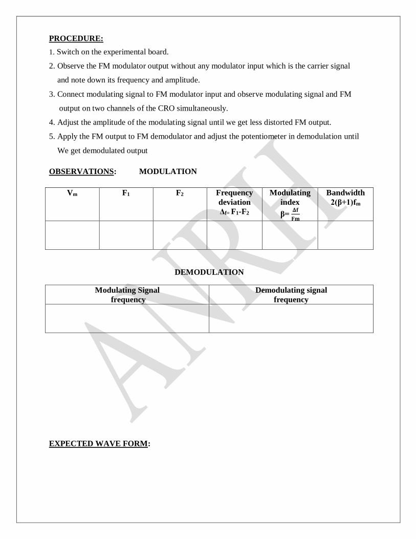
OBSERVATIONS: MODULATION
Vm F1 F2 Frequency
deviation
Δf= F1-F2
Modulating
index
β= 𝚫𝐟
𝐅𝐦
Bandwidth
2(β+1)fm
DEMODULATION
Modulating Signal
frequency
Demodulating signal
frequency
EXPECTED WAVE FORM:
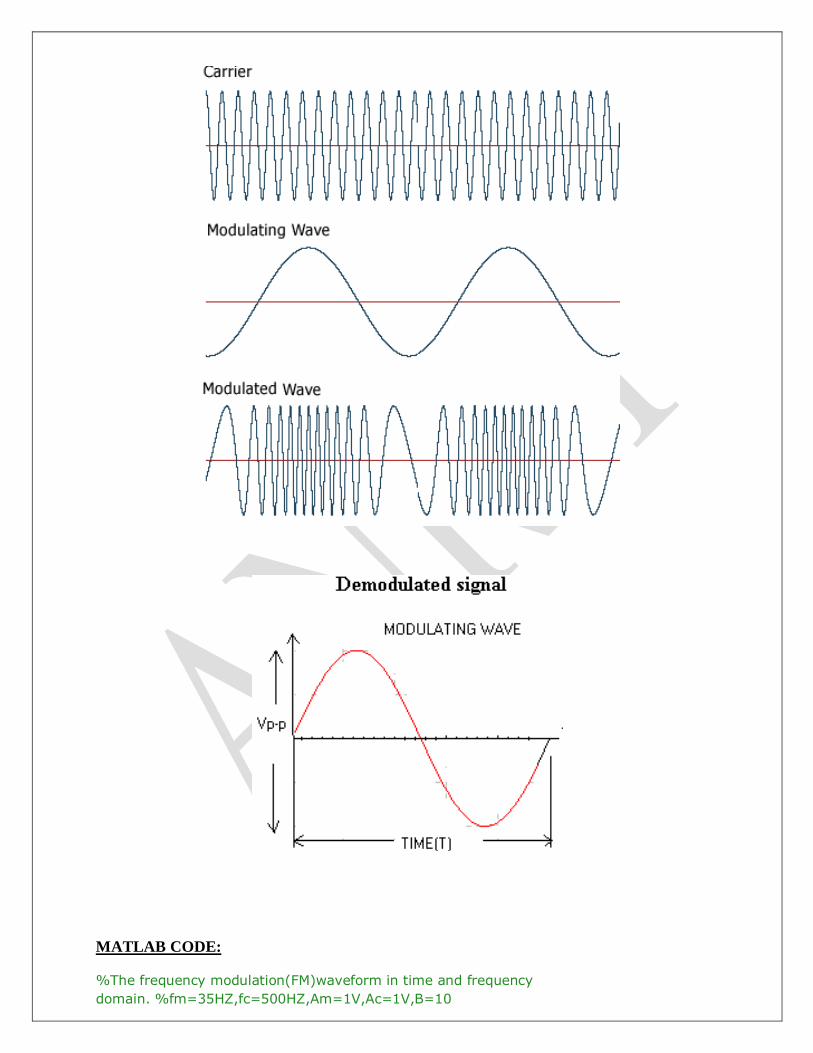
MATLAB CODE:
%The frequency modulation(FM)waveform in time and frequency
domain. %fm=35HZ,fc=500HZ,Am=1V,Ac=1V,B=10
Clc;
Clear all;
Close all;
fs=10000;
Ac=1;
Am=1;
fm=35;
fc=500;
B=10;
t=(0:0.1*fs)/fs;
wc=2*pi*fc;
wm=2*pi*fm;
m_t=Am*cos(wm*t);
subplot(5,1,1);
plot(t,m_t);
title('Modulating or Message signal(fm=35Hz)');
c_t=Ac*cos(wc*t);
subplot(5,1,2);
plot(t,c_t);
title('Carriersignal(fm=500Hz)');
s_t=Ac*cos((wc*t)+B*sin(wm*t));
subplot(5,1,3);
plot(t,s_t);
title('Modulatedsignal');
d=demod(s_t,fc,fs,'fm');
subplot(5,1,4);
plot(t,d);
title('demodulated signal');
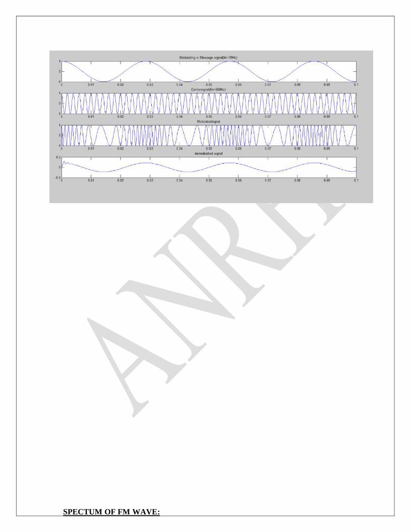
SPECTUM OF FM WAVE:
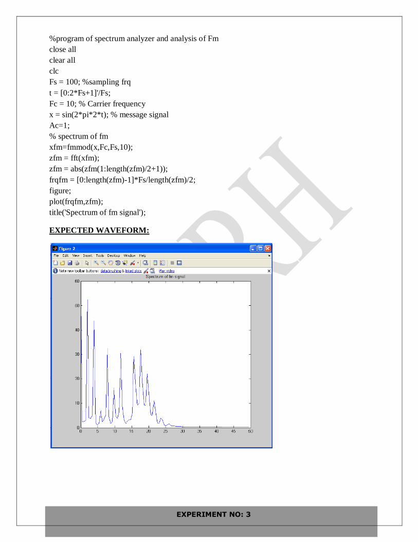
%program of spectrum analyzer and analysis of Fm
close all
clear all
clc
Fs = 100; %sampling frq
t = [0:2*Fs+1]'/Fs;
Fc = 10; % Carrier frequency
x = sin(2*pi*2*t); % message signal
Ac=1;
% spectrum of fm
xfm=fmmod(x,Fc,Fs,10);
zfm = fft(xfm);
zfm = abs(zfm(1:length(zfm)/2+1));
frqfm = [0:length(zfm)-1]*Fs/length(zfm)/2;
figure;
plot(frqfm,zfm);
title('Spectrum of fm signal');
EXPECTED WAVEFORM:
EXPERIMENT NO: 3
DSB-SC MODULATION & DETECTION
AIM:
To study and observe the function of Balanced Modulator and Demodulator, observe its
efficiency
APPARATUS:
1. Amplitude Modulation & De modulation trainer kit.
2. C.R.O (20MHz)
3. Function generator (1MHz).
4. Connecting cords & probes.
5. PC with windows(95/98/XP/NT/2000)
6. DSBSC Modulation & De modulation trainer kit.
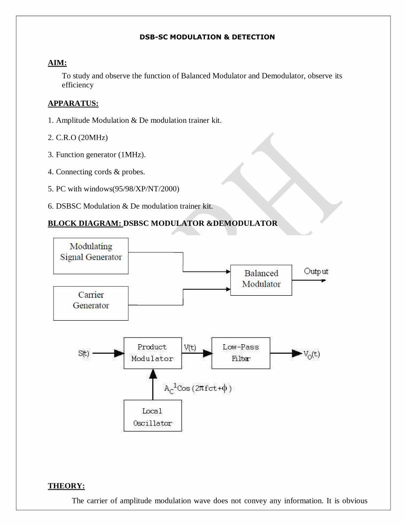
BLOCK DIAGRAM: DSBSC MODULATOR &DEMODULATOR
THEORY:
The carrier of amplitude modulation wave does not convey any information. It is obvious
from the fact that the carrier component remains constant in amplitude and frequency. No matter
what the modulating signal does. It is thus, seen that no information is conveyed by the carrier. If
the carrier is suppressed, only the side bands remains and a saving of two third powers can achieve
at 100% modulation such suppression of carrier doesn’t affect the massage signal in any way. This
idea has resulted in the evolution of suppressed carrier modulation. Thus, the short coming of the
conventional AM in regard of power wastage is overcome by suppressing the carrier from the
modulated wave resulting in double side band suppressed carrier modulation. A balanced is used to
generate DSBSC wave. A DSBSC signal is basically the product of the base band signal and the
carrier wave.
S(t) = m(t) *c(t)
Where m(t) is base band signal
C(t) is carrier signal C(t)
= Ac cost 2Π fct The modulated wave under goes a phase reversal when ever base band signal m(t) crosses
zero.Spectrum of base band signal
S(f) = AC/2 [(M(f-fc) + M(f+fc)] Where M (f) is the fourier trans form of m(t)
Ac is carrier amplitude And fc is frequency of the carrier. The band width of DSBSC signal is same as that of conventional AM i.e., 2W.
The base band signal m(t) can be uniquely recovered from a DSB-SC wave S(t) by first
multiplying s(t) with a locally generated sinusoidal wave and then low-pass filtering the product, as
in fig. below. It is assumed that the local oscillator signal is exactly coherent or synchronized, in
both frequency and phase, with the carrier wave C(t) used in the product modulator to generate S(t).
This method of demodulation is known as Coherent or Synchronous demodulation.
PROCEDURE: 1. Apply DSB-SC signal to DSB-SC signal input of the synchronous detector and RF generator
output to RF input of synchronous detector. 2. Observe the synchronous detector output on CRO and compare it with the original AF
signal.
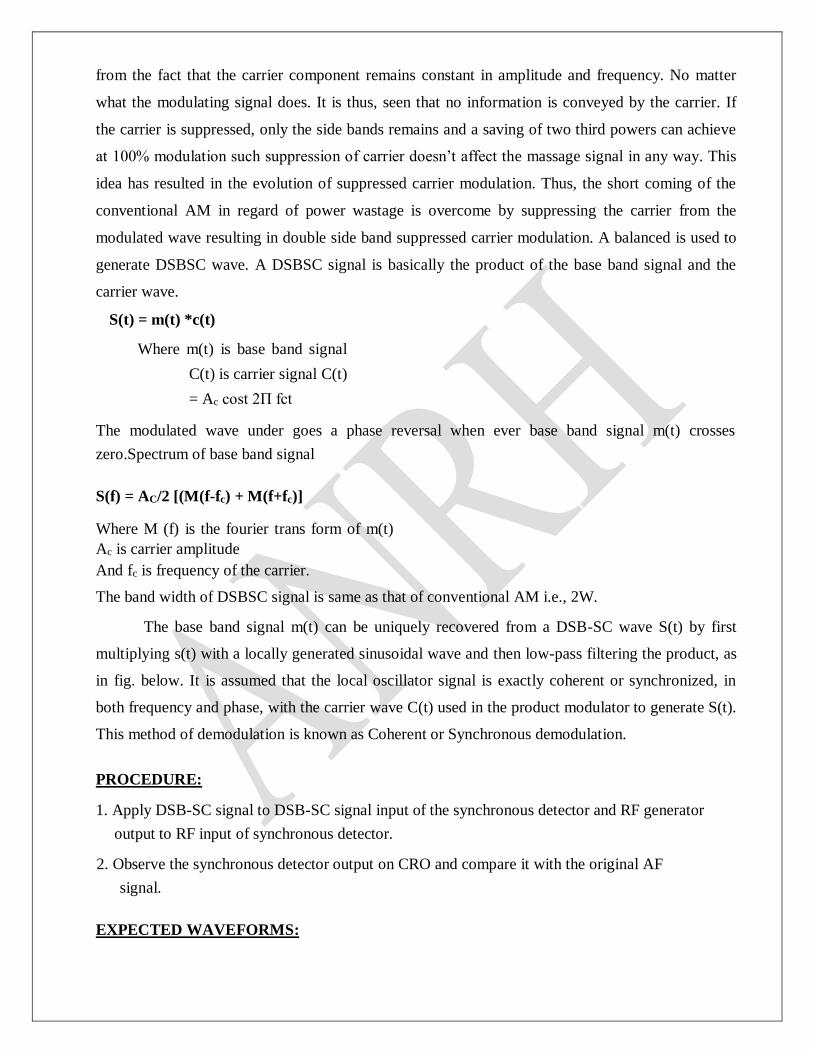
EXPECTED WAVEFORMS:
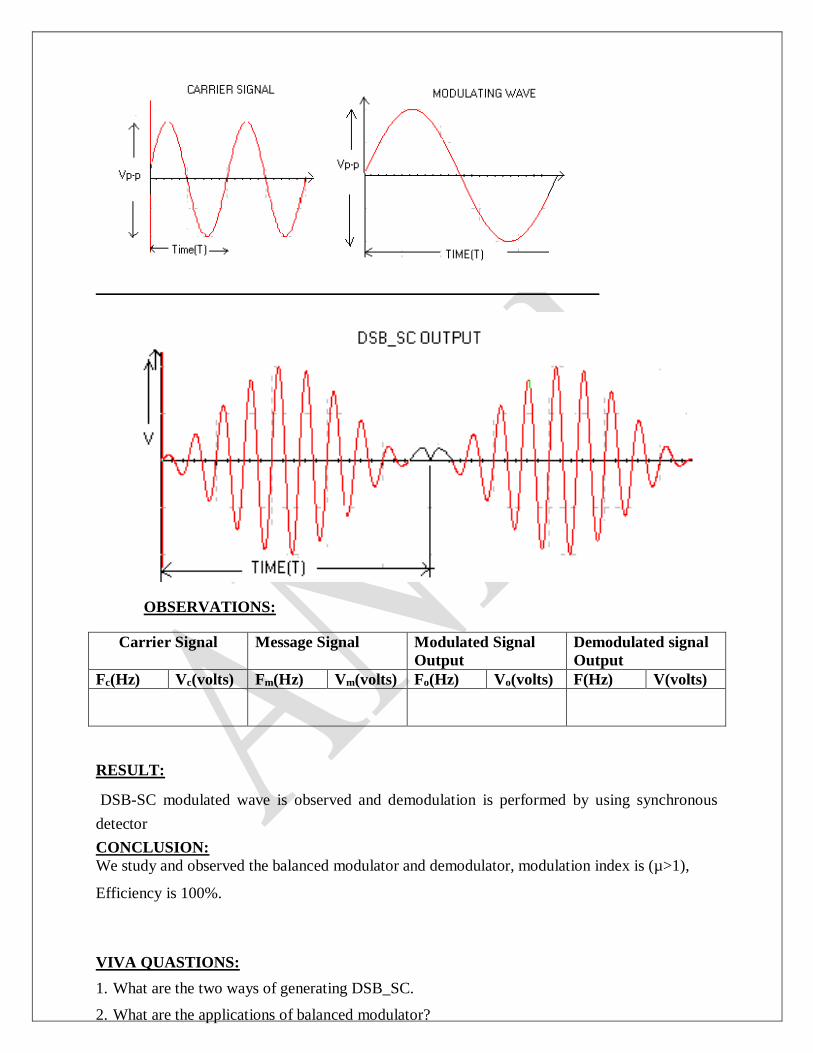
OBSERVATIONS:
Carrier Signal Message Signal Modulated Signal
Output
Demodulated signal
Output
Fc(Hz) Vc(volts) Fm(Hz) Vm(volts) Fo(Hz) Vo(volts) F(Hz) V(volts)
RESULT: DSB-SC modulated wave is observed and demodulation is performed by using synchronous
detector
CONCLUSION:
We study and observed the balanced modulator and demodulator, modulation index is (µ>1),
Efficiency is 100%.
VIVA QUASTIONS: 1. What are the two ways of generating DSB_SC. 2. What are the applications of balanced modulator?
3. What are the advantages of suppressing the carrier? 4. What are the advantages of balanced modulator? 5. What are the advantages of Ring modulator? 6. Write the expression for the output voltage of a balanced modulator? 7. Give any two methods to avoid errors in synchrouns demodulator? 8. What is quadrature null effect in synchronous demodulator? 9.What is beats in synchronous detector? 10.Give the block diagram of synchronous detector?
11.Give the working principle of coastas receiver.
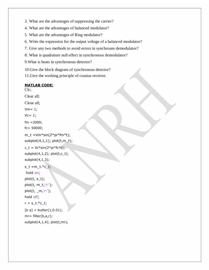
MATLAB CODE:
Clc;
Clear all;
Close all;
Vm= 1; Vc= 1; fm =2000;
fc= 50000; m_t =Vm*sin(2*pi*fm*t);
subplot(4,1,1); plot(t,m_t); c_t = Vc*sin(2*pi*fc*t);
subplot(4,1,2); plot(t,c_t);
subplot(4,1,3); s_t =m_t.*c_t;
hold on;
plot(t, s_t);
plot(t, m_t,'r:');
plot(t, _m,'r:');
hold off; r = s_t.*c_t; [b a] = butter(1,0.01);
mr= filter(b,a,r);
subplot(4,1,4); plot(t,mr);
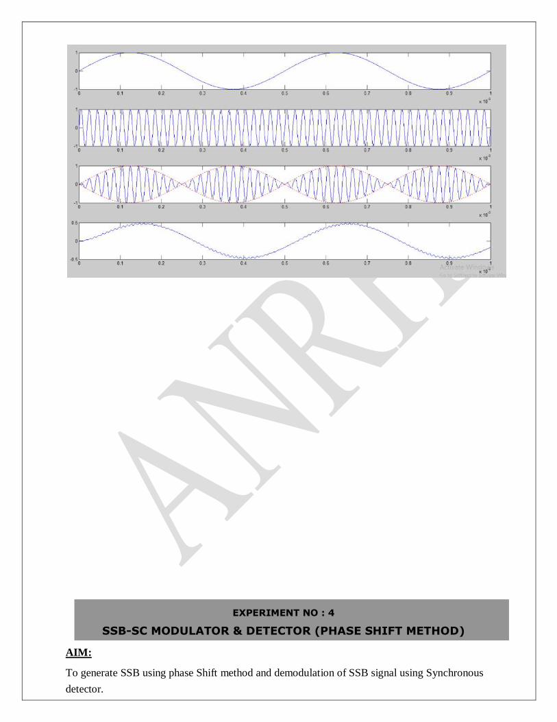
EXPERIMENT NO : 4
SSB-SC MODULATOR & DETECTOR (PHASE SHIFT METHOD)
AIM: To generate SSB using phase Shift method and demodulation of SSB signal using Synchronous
detector.
APPARATUS:
1. Amplitude Modulation & De modulation trainer kit.
2. C.R.O (20MHz)
3. Function generator (1MHz).
4. Connecting cords & probes.
5. PC with windows(95/98/XP/NT/2000)
6. SSBSC Modulation & De modulation trainer kit.
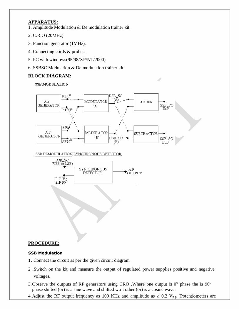
BLOCK DIAGRAM:
PROCEDURE:
SSB Modulation 1. Connect the circuit as per the given circuit diagram. 2 .Switch on the kit and measure the output of regulated power supplies positive and negative
voltages. 3. Observe the outputs of RF generators using CRO .Where one output is 00 phase the is 900
phase shifted (or) is a sine wave and shifted w.r.t other (or) is a cosine wave. 4. Adjust the RF output frequency as 100 KHz and amplitude as ≥ 0.2 Vp-p (Potentiometers are
provided to vary the output amplitude & frequency).
5. Observe the two outputs of AF generator using CRO. 6. Select the required frequency (2 kHz, 4 kHz and 6 kHz) form the switch positions for A.F. 7. Adjust the gain of the oscillator by varying the AGC potentiometer and keep the amplitude of 10Vp-p. 8. Measure and record the above seen signals & their frequencies on CRO. 9. Set the amplitude of the R.F signal to 0. 2Vp-p and A.F signal amplitude to 8Vp-p and
connect AF-00 and RF-900 to inputs of balanced modulator A and observe DSB-SC (A) output on
CRO. Connect AF-900 and RF-00 to inputs of balanced modulator B and observe the DSB-SC
(B) out put on CRO and plot the same on graph. 10. To get SSB lower side band signal connect balanced modulator outputs(DSB-SC) to
subtractor and observe the output wave form on CRO and plot the same on graph. 11. To get SSB upper side band signal, connect the output of balanced modulator outputs to
summer circuit and observe the output waveform on CRO and plot the same on graph.
12. Calculate theoretical frequency of SSB (LSB & USB) and compare it with practical value. SSB Demodulation 1. Connect SSB signal from the summer or sub-tractor to the SSB signal input of Synchronous
detector and RF signal (0o) to the RF input of the synchronous detector.
2. Observe the detector output on CRO and compare it with the modulating signal.
OBSERVATIONS:
Carrier
signal
Modulating
signal
Balanced
modulator-
A
Balanced
Modulator-
B
Adder/Subtractor
Output
Synchronus
detector
Fc Vc Fm Vm Vmax Vmin Vmax Vmin Vmax Vmin Fd Vd
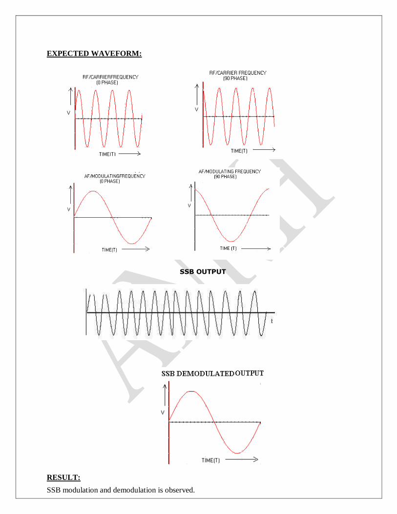
EXPECTED WAVEFORM:
SSB OUTPUT
RESULT: SSB modulation and demodulation is observed.
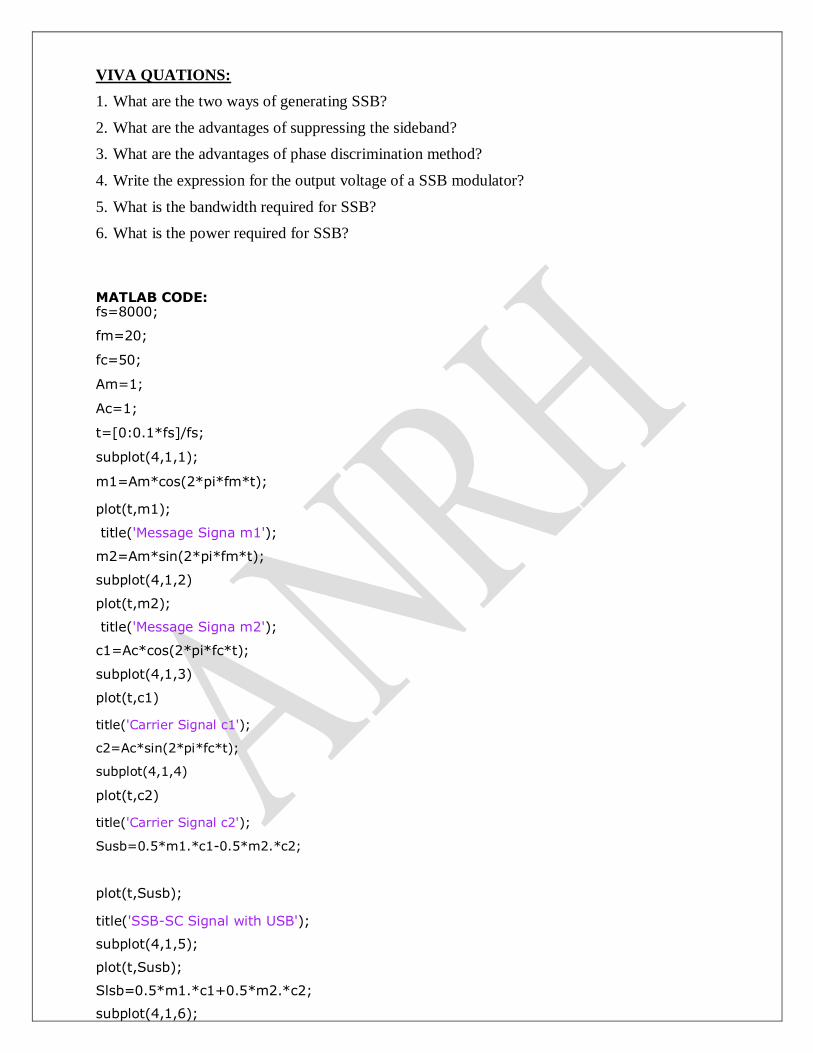
VIVA QUATIONS: 1. What are the two ways of generating SSB? 2. What are the advantages of suppressing the sideband? 3. What are the advantages of phase discrimination method? 4. Write the expression for the output voltage of a SSB modulator? 5. What is the bandwidth required for SSB? 6. What is the power required for SSB?
MATLAB CODE: fs=8000; fm=20; fc=50; Am=1; Ac=1; t=[0:0.1*fs]/fs; subplot(4,1,1); m1=Am*cos(2*pi*fm*t); plot(t,m1);
title('Message Signa m1');
m2=Am*sin(2*pi*fm*t);
subplot(4,1,2)
plot(t,m2);
title('Message Signa m2');
c1=Ac*cos(2*pi*fc*t);
subplot(4,1,3)
plot(t,c1) title('Carrier Signal c1');
c2=Ac*sin(2*pi*fc*t);
subplot(4,1,4)
plot(t,c2) title('Carrier Signal c2');
Susb=0.5*m1.*c1-0.5*m2.*c2;
plot(t,Susb); title('SSB-SC Signal with USB');
subplot(4,1,5);
plot(t,Susb);
Slsb=0.5*m1.*c1+0.5*m2.*c2;
subplot(4,1,6);
plot(t,Slsb); title('SSB-SC Signal with LSB');
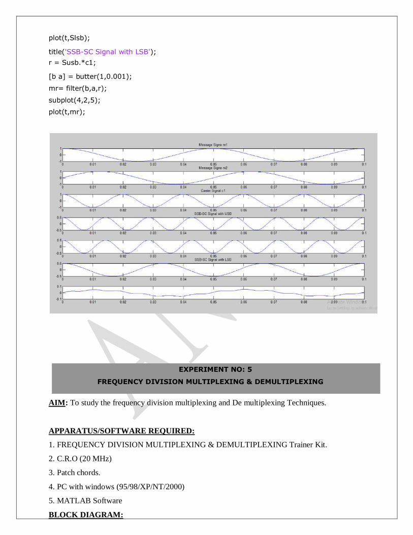
r = Susb.*c1; [b a] = butter(1,0.001);
mr= filter(b,a,r);
subplot(4,2,5);
plot(t,mr);
EXPERIMENT NO: 5
FREQUENCY DIVISION MULTIPLEXING & DEMULTIPLEXING
AIM: To study the frequency division multiplexing and De multiplexing Techniques.
APPARATUS/SOFTWARE REQUIRED:
1. FREQUENCY DIVISION MULTIPLEXING & DEMULTIPLEXING Trainer Kit.
2. C.R.O (20 MHz)
3. Patch chords.
4. PC with windows (95/98/XP/NT/2000)
5. MATLAB Software
BLOCK DIAGRAM:
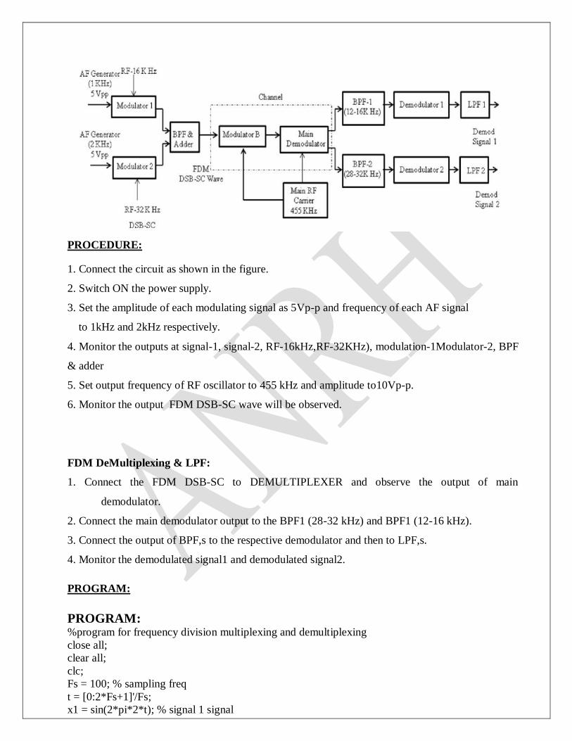
PROCEDURE:
1. Connect the circuit as shown in the figure.
2. Switch ON the power supply.
3. Set the amplitude of each modulating signal as 5Vp-p and frequency of each AF signal
to 1kHz and 2kHz respectively.
4. Monitor the outputs at signal-1, signal-2, RF-16kHz,RF-32KHz), modulation-1Modulator-2, BPF
& adder
5. Set output frequency of RF oscillator to 455 kHz and amplitude to10Vp-p.
6. Monitor the output FDM DSB-SC wave will be observed.
FDM DeMultiplexing & LPF:
1. Connect the FDM DSB-SC to DEMULTIPLEXER and observe the output of main
demodulator.
2. Connect the main demodulator output to the BPF1 (28-32 kHz) and BPF1 (12-16 kHz).
3. Connect the output of BPF,s to the respective demodulator and then to LPF,s.
4. Monitor the demodulated signal1 and demodulated signal2.
PROGRAM:
PROGRAM: %program for frequency division multiplexing and demultiplexing
close all;
clear all;
clc;
Fs = 100; % sampling freq
t = [0:2*Fs+1]'/Fs;
x1 = sin(2*pi*2*t); % signal 1 signal
z1 = fft(x1);
z1=abs(z1);
x2 = sin(2*pi*10*t); % signal 2 signal
z2 = fft(x2);
z2=abs(z2);
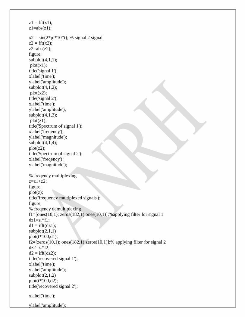
figure;
subplot(4,1,1);
plot(x1);
title('signal 1');
xlabel('time');
ylabel('amplitude');
subplot(4,1,2);
plot(x2);
title('signal 2');
xlabel('time');
ylabel('amplitude');
subplot(4,1,3);
plot(z1);
title('Spectrum of signal 1');
xlabel('freqency');
ylabel('magnitude');
subplot(4,1,4);
plot(z2);
title('Spectrum of signal 2');
xlabel('freqency');
ylabel('magnitude');
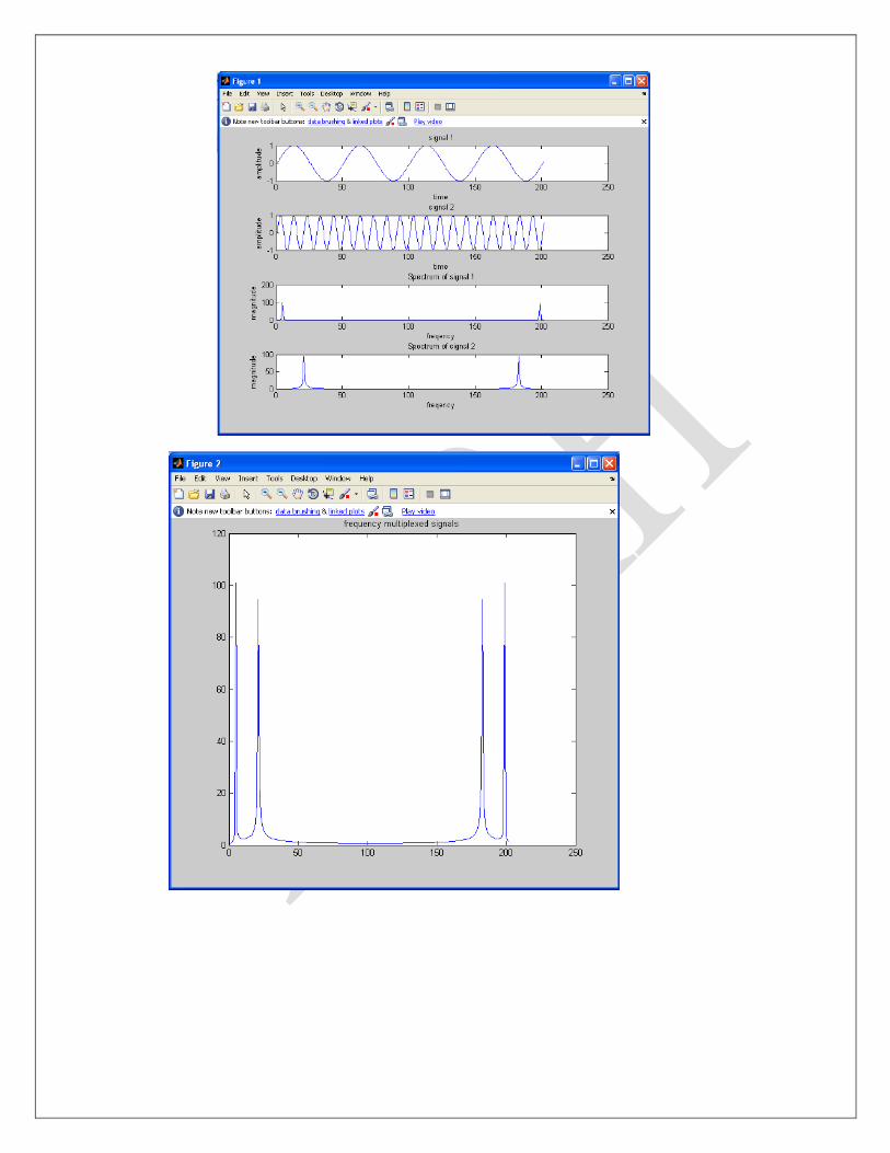
% freqency multiplexing
z=z1+z2;
figure;
plot(z);
title('frequency multiplexed signals');
figure;
% freqency demultiplexing
f1=[ones(10,1); zeros(182,1);ones(10,1)];%applying filter for signal 1
dz1=z.*f1;
d1 = ifft(dz1);
subplot(2,1,1)
plot(t*100,d1);
f2=[zeros(10,1); ones(182,1);zeros(10,1)];% applying filter for signal 2
dz2=z.*f2;
d2 = ifft(dz2);
title('recovered signal 1');
xlabel('time');
ylabel('amplitude');
subplot(2,1,2)
plot(t*100,d2);
title('recovered signal 2');
xlabel('time');
ylabel('amplitude');
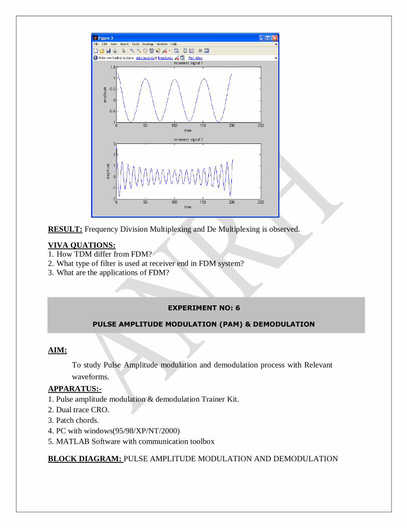
RESULT: Frequency Division Multiplexing and De Multiplexing is observed.
VIVA QUATIONS:
1. How TDM differ from FDM?
2. What type of filter is used at receiver end in FDM system?
3. What are the applications of FDM?
EXPERIMENT NO: 6
PULSE AMPLITUDE MODULATION (PAM) & DEMODULATION
AIM:
To study Pulse Amplitude modulation and demodulation process with Relevant
waveforms.
APPARATUS:-
1. Pulse amplitude modulation & demodulation Trainer Kit.
2. Dual trace CRO.
3. Patch chords.
4. PC with windows(95/98/XP/NT/2000)
5. MATLAB Software with communication toolbox
BLOCK DIAGRAM: PULSE AMPLITUDE MODULATION AND DEMODULATION
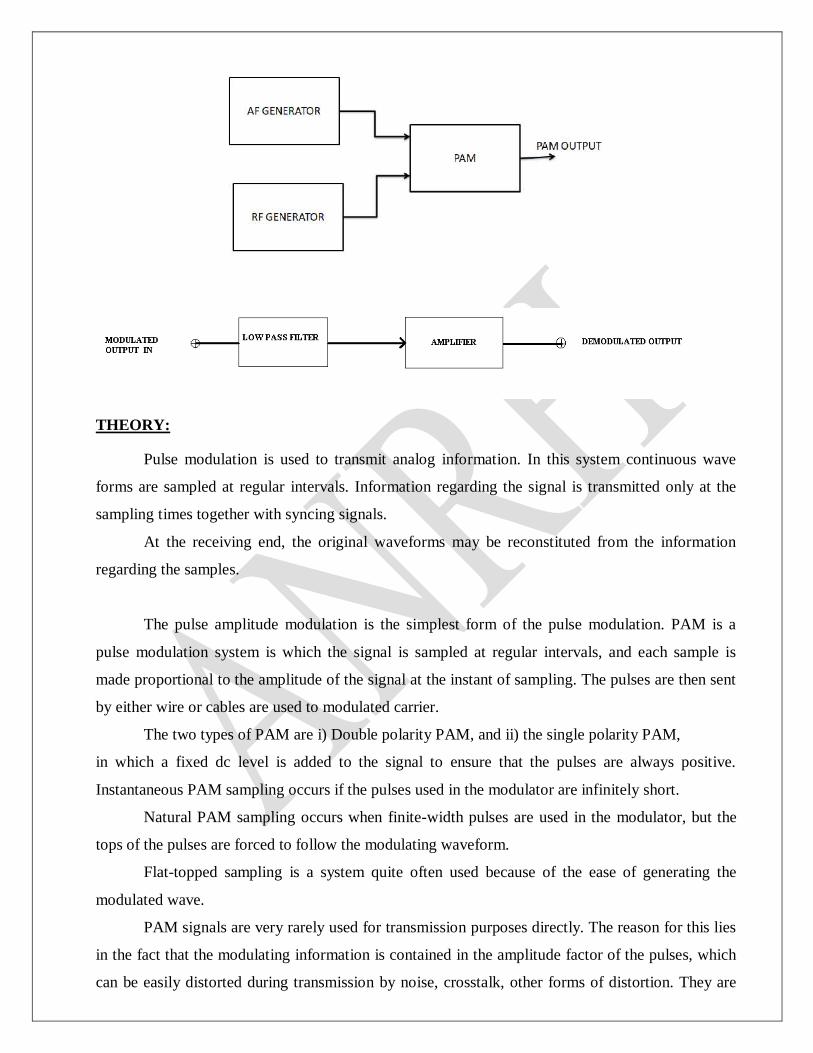
THEORY:
Pulse modulation is used to transmit analog information. In this system continuous wave
forms are sampled at regular intervals. Information regarding the signal is transmitted only at the
sampling times together with syncing signals.
At the receiving end, the original waveforms may be reconstituted from the information
regarding the samples.
The pulse amplitude modulation is the simplest form of the pulse modulation. PAM is a
pulse modulation system is which the signal is sampled at regular intervals, and each sample is
made proportional to the amplitude of the signal at the instant of sampling. The pulses are then sent
by either wire or cables are used to modulated carrier.
The two types of PAM are i) Double polarity PAM, and ii) the single polarity PAM,
in which a fixed dc level is added to the signal to ensure that the pulses are always positive.
Instantaneous PAM sampling occurs if the pulses used in the modulator are infinitely short.
Natural PAM sampling occurs when finite-width pulses are used in the modulator, but the
tops of the pulses are forced to follow the modulating waveform.
Flat-topped sampling is a system quite often used because of the ease of generating the
modulated wave.
PAM signals are very rarely used for transmission purposes directly. The reason for this lies
in the fact that the modulating information is contained in the amplitude factor of the pulses, which
can be easily distorted during transmission by noise, crosstalk, other forms of distortion. They are
used frequently as an intermediate step in other pulsemodulating methods, especially where time-
division multiplexing is used.
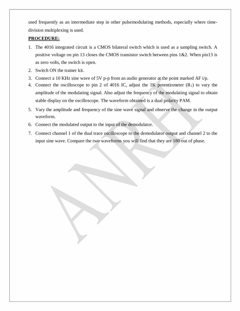
PROCEDURE: 1. The 4016 integrated circuit is a CMOS bilateral switch which is used as a sampling switch. A
positive voltage on pin 13 closes the CMOS transistor switch between pins 1&2. When pin13 is
as zero volts, the switch is open. 2. Switch ON the trainer kit. 3. Connect a 10 KHz sine wave of 5V p-p from an audio generator at the point marked AF i/p. 4. Connect the oscilloscope to pin 2 of 4016 IC, adjust the 1K potentiometer (R1) to vary the
amplitude of the modulating signal. Also adjust the frequency of the modulating signal to obtain
stable display on the oscilloscope. The waveform obtained is a dual polarity PAM. 5. Vary the amplitude and frequency of the sine wave signal and observe the change in the output
waveform. 6. Connect the modulated output to the input of the demodulator. 7. Connect channel 1 of the dual trace oscilloscope to the demodulator output and channel 2 to the
input sine wave. Compare the two waveforms you will find that they are 180 out of phase.
EXPECTED WAVE FORMS:
RESULT: Pulse amplitude modulation and demodulation is observed and their respective wave forms
are plotted. CONCLUSION:
In Pulse Amplitude Modulation we observed that the characteristic parameter (amplitude) of
carrier is varied according to the amplitude of the message signal, the samples are taken at
regular intervals of time. Each sample is a pulse whose amplitude is determined by the amplitude
of the variable at the instant of time at which the samples are taken, a reasonable approximating
of the signal being sampled can be constructed at the receiving end
VIVA QUASTIONS: 1. TDM is possible for sampled signals. What kind of multiplexing can be used in continuous
modulation systems? 2. What is the minimum rate at which a speech signal can be sampled for the purpose of PAM? 3. What is cross talk in the context of time division multiplexing? 4. Which is better, natural sampling or flat topped sampling and why? 5. Why a dc offset has been added to the modulating signal in this board? Was it essential for
the working of the modulator? Explain. 7. Study about the frequency spectrum of PAM signal and derive mathematical expression for it? 8. Explain the modulation circuit operation? 9. Explain the demodulation circuit operation?
MATLAB CODE: PROGRAM: clc; close all;
clear all; t=0:1/6000:((10/1000)-(1/6000));
xa=sin(2*pi*100*abs(t)); Ts=32; x=sin(2*pi*600*(Ts*t)); X=fft(xa,abs(x)); subplot(3,1,1); plot(x,a);
grid subplot(3,1,2); stem(X);
grid
Y=ifft(xa,X); subplot(3,1,3); plot(Y);
grid
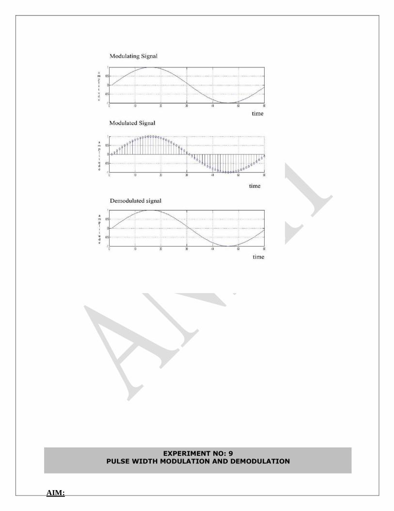
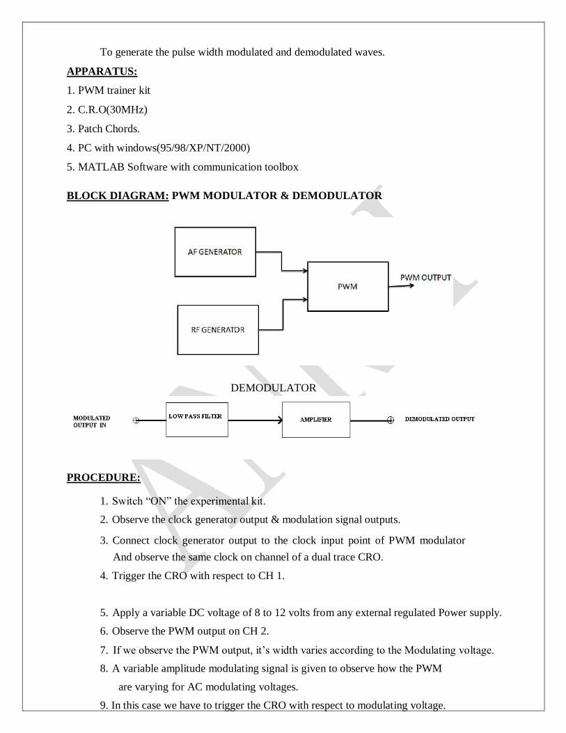
EXPERIMENT NO: 9 PULSE WIDTH MODULATION AND DEMODULATION
AIM:
To generate the pulse width modulated and demodulated waves.
APPARATUS:
1. PWM trainer kit
2. C.R.O(30MHz)
3. Patch Chords.
4. PC with windows(95/98/XP/NT/2000)
5. MATLAB Software with communication toolbox
BLOCK DIAGRAM: PWM MODULATOR & DEMODULATOR
DEMODULATOR
PROCEDURE:
1. Switch “ON” the experimental kit.
2. Observe the clock generator output & modulation signal outputs.
3. Connect clock generator output to the clock input point of PWM modulator
And observe the same clock on channel of a dual trace CRO.
4. Trigger the CRO with respect to CH 1.
5. Apply a variable DC voltage of 8 to 12 volts from any external regulated Power supply.
6. Observe the PWM output on CH 2.
7. If we observe the PWM output, it’s width varies according to the Modulating voltage.
8. A variable amplitude modulating signal is given to observe how the PWM
are varying for AC modulating voltages.
9. In this case we have to trigger the CRO with respect to modulating voltage.
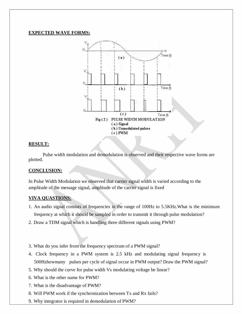
EXPECTED WAVE FORMS:
RESULT:
Pulse width modulation and demodulation is observed and their respective wave forms are
plotted.
CONCLUSION:
In Pulse Width Modulation we observed that carrier signal width is varied according to the
amplitude of the message signal, amplitude of the carrier signal is fixed
VIVA QUASTIONS: 1. An audio signal consists of frequencies in the range of 100Hz to 5.5KHz.What is the minimum
frequency at which it should be sampled in order to transmit it through pulse modulation? 2. Draw a TDM signal which is handling three different signals using PWM?
3. What do you infer from the frequency spectrum of a PWM signal? 4. Clock frequency in a PWM system is 2.5 kHz and modulating signal frequency is
500Hzhowmany pulses per cycle of signal occur in PWM output? Draw the PWM signal? 5. Why should the curve for pulse width Vs modulating voltage be linear? 6. What is the other name for PWM? 7. What is the disadvantage of PWM? 8. Will PWM work if the synchronization between Tx and Rx fails? 9. Why integrator is required in demodulation of PWM?
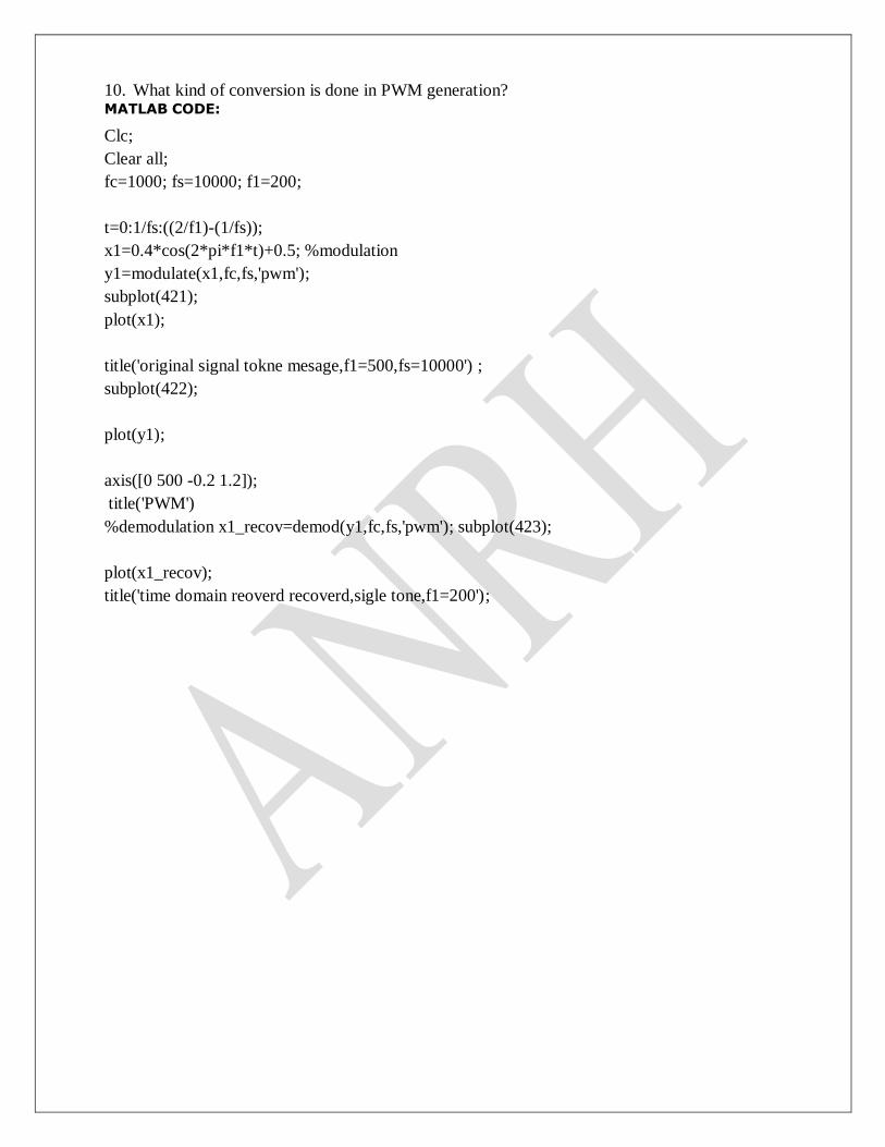
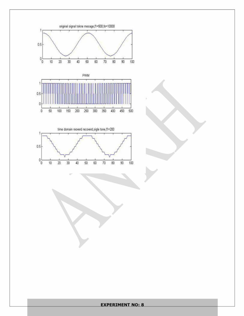
10. What kind of conversion is done in PWM generation? MATLAB CODE:
Clc;
Clear all;
fc=1000; fs=10000; f1=200;
t=0:1/fs:((2/f1)-(1/fs));
x1=0.4*cos(2*pi*f1*t)+0.5; %modulation
y1=modulate(x1,fc,fs,'pwm');
subplot(421);
plot(x1);
title('original signal tokne mesage,f1=500,fs=10000') ;
subplot(422);
plot(y1);
axis([0 500 -0.2 1.2]);
title('PWM')
%demodulation x1_recov=demod(y1,fc,fs,'pwm'); subplot(423);
plot(x1_recov);
title('time domain reoverd recoverd,sigle tone,f1=200');
EXPERIMENT NO: 8
PULSE POSITION MODULATION AND DEMODULATION
AIM:
To study the generation Pulse Position Modulation (PPM) and Demodulation.
APPARATUS:
1. Pulse Position Modulation (PPM) and demodulation Trainer Kit.
2. C.R.O(30MHz)
3. Patch chords.
4. PC with windows(95/98/XP/NT/2000)
5. MATLAB Software with communication toolbox
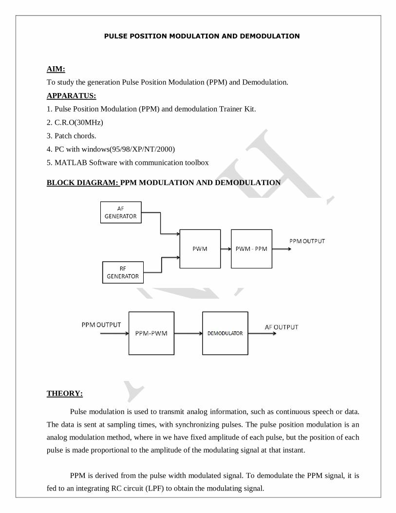
BLOCK DIAGRAM: PPM MODULATION AND DEMODULATION
THEORY:
Pulse modulation is used to transmit analog information, such as continuous speech or data.
The data is sent at sampling times, with synchronizing pulses. The pulse position modulation is an
analog modulation method, where in we have fixed amplitude of each pulse, but the position of each
pulse is made proportional to the amplitude of the modulating signal at that instant.
PPM is derived from the pulse width modulated signal. To demodulate the PPM signal, it is
fed to an integrating RC circuit (LPF) to obtain the modulating signal.
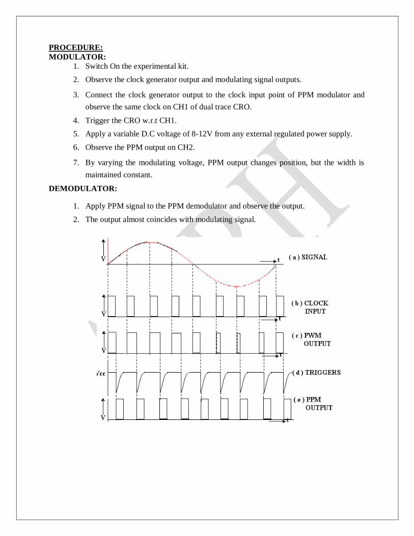
PROCEDURE: MODULATOR:
1. Switch On the experimental kit.
2. Observe the clock generator output and modulating signal outputs.
3. Connect the clock generator output to the clock input point of PPM modulator and
observe the same clock on CH1 of dual trace CRO.
4. Trigger the CRO w.r.t CH1.
5. Apply a variable D.C voltage of 8-12V from any external regulated power supply.
6. Observe the PPM output on CH2.
7. By varying the modulating voltage, PPM output changes position, but the width is
maintained constant. DEMODULATOR:
1. Apply PPM signal to the PPM demodulator and observe the output.
2. The output almost coincides with modulating signal.
RESULT:
Pulse position modulation and demodulation is observed and their respective wave forms are plotted.
VIVA QUASTIONS:
1. Define and describe PPM?
2. Explain with waveforms how PPM is derived from PWM.
3. What is the fundamental difference between pulse modulation, on the one hand, and
frequency and amplitude modulation on the other?
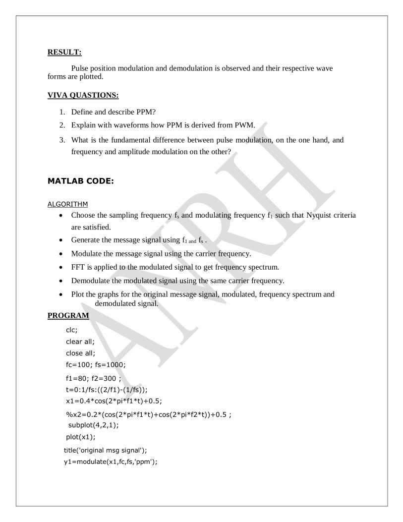
MATLAB CODE: ALGORITHM
Choose the sampling frequency fs and modulating frequency f1 such that Nyquist criteria
are satisfied.
Generate the message signal using f1 and fs .
Modulate the message signal using the carrier frequency.
FFT is applied to the modulated signal to get frequency spectrum.
Demodulate the modulated signal using the same carrier frequency.
Plot the graphs for the original message signal, modulated, frequency spectrum and
demodulated signal.
PROGRAM
clc;
clear all;
close all;
fc=100; fs=1000;
f1=80; f2=300 ;
t=0:1/fs:((2/f1)-(1/fs));
x1=0.4*cos(2*pi*f1*t)+0.5;
%x2=0.2*(cos(2*pi*f1*t)+cos(2*pi*f2*t))+0.5 ;
subplot(4,2,1);
plot(x1);
title('original msg signal');
y1=modulate(x1,fc,fs,'ppm');
subplot(4,2,2);
plot(y1)
axis([0 50 -0.2 1.2]); title('ppm one of f1,fc=1000,f1=80 ');
fx1=abs(fft(y1,1024)) ;
fx1=[fx1(512:1024) fx1(1:513)];
f=[(511*fs/1024):(fs/1024):(512*fs/1024)];
subplot(4,2,3);
plot(fx1);
title('freq des ppm signal tone,fc=1000');
x1_recov = demod(y1,fc,fs,'ppm');
subplot(4,2,4);
plot(x1_recov);
title('time domain recovered signal');
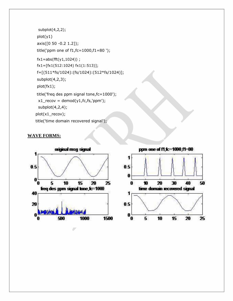
WAVE FORMS:
EXPERIMENT NO: 9
AMPLITUDE MODULATION AND DEMODULATION
AIM:
To analyze a PCM system and interpret the modulated and demodulated waveforms for a
sampling frequency of 4 KHz.
APPARATUS:
1. PCM modulator trainer
2. PCM Demodulator trainer
3. C.R.O(30MHz)
4. Patch chords.
5. PC with windows(95/98/XP/NT/2000)
6. MATLAB Software with communication toolbox
INTRODUCTION
In Pulse code modulation (PCM) only certain discrete values are allowed for the
modulating signals. The modulating signal is sampled, as in other forms of pulse modulation.
But any sample falling within a specified range of values is assigned a discrete value. Each value
is assigned a pattern of pulses and the signal transmitted by means of this code. The electronic
circuit that produces the coded pulse train from the modulating waveform is termed a coder or
encoder. A suitable decoder must be used at the receiver in order to extract the original
information from the transmitted pulse train.
This PCM system consists of
PCM Modulator
1. Regulated power supply
2. Audio Frequency signal generator
3. Sample & Hold circuit
4. 8 Bit A/D Converter
5. 8 Bit Parallel-Serial Shift register
6. Clock generator/Timing circuit
7. DC source
2.3.2. PCM Demodulator
1. Regulated power supply
2. 8 Bit Serial-Parallel to shift register
3. 8 Bit D/A converter
4. Clock generator
5. Timing circuit
6. Passive low pass filter
7. Audio amplifiers
BLOCK DIAGRAM: PCM MODULATOR & DEMODULATOR
Regulated power supply (68M & 68D):
This consists of a bridge rectifier followed by capacitor filters and three terminal
regulators 7805 and 7905 to provide regulated DC voltages of +5V and +12V @ 300Ma each to
the on board circuits. These supplies have been internally connected to the circuits, so no
external connections are required for operation.
Audio Frequency (AF) Signal generator (68M):
Sine wave signal of 200Hz is generated to use as a modulating (message or information)
signal to be transmitted. This is an Op-Amp based Wein bridge Oscillators using IC TL084. IC
TL084 is a FET input general purpose Operational Amplifier. Amplitude control is provided in
the circuit to vary the output amplitude of AF signal.
Clock generator/Timing circuit (68M & 68D):
A TTL compatible clock signal of 64 KHz and 4KHz frequency are provided on board to
use as a clock to the various circuits in the system. This circuit is a astable multivibrator using
555 timer followed by a buffer and frequency dividers.
DC source (68M):
A 0 to +5V variable DC voltage is provided on board to use as a modulating signal
instead of AF signal. This is useful to study step by operation of PCM modulation and
demodulation. This is a simple circuit consisting of potentiometer and fixed power supply.
Low pass filters (68D):
This is a series of simple RC networks provided on board to smoothen the output of the
D/A converter output (stair case signal). RC values are chosen such that the cutoff frequency
would be at 200Hz
Amplifiers (68D):
This is an Op-amp (IC TL084) based non-inverting variable gain amplifiers provided on
board to amplify the recovered message singles i.e. output of the Low pass filter to desired level.
Amplitude control is provided in circuit to vary the gain of the amplifier between 0 and 3.
AC/DC Switch facilitates to couple the input signal through capacitor or directly to the amplifier
input.
Sample & Hold circuit (AET-68M):
This block (circuit) is a combination of buffer, level shifting network and sample & hold
network. Op- amp IC TL084 is connected as buffer followed by non-inverting summer circuit.
One of the inputs of summer is connected a voltage divider network and other being drawn as
input. A dedicated sample& hold integrated circuit LF 398 is used as an active component
followed by buffer. The LF198/LF298/LF398 is monolithic sample-and-hold circuits which
utilize BI-FET technology to obtain ultra-high dc accuracy with fast acquisition of signal and
low droop rate. Operating as a unity gain follower, dc gain accuracy is 0.002% typical and
acquisition time is as low as 6μs to 0.01%. A bipolar input stage is used to achieve low offset
voltage and wide bandwidth.
Input offset adjust is accomplished with a single pin, and does not degrade input offset
drift. The wide bandwidth allows the LF198 to be included inside the feedback loop of 1 MHz op
amps without having stability problems. Input impedance of 1010(Ohm) allows high source
impedance to be used without degrading accuracy.
P-channel junction FET’s are combined with bipolar devices in the output amplifier to
give droop rates as low as 5mV/min with a 1μf hold capacitor. The JFET’s have much lower
noise than MOS devices used in previous designs and do not exhibit high temperature
instabilities. The overall design guarantees no feed-through from input to output in the hold
mode, even for input signals equal to the supply voltages.
Logic inputs on the LF198 are fully differential with low current, allowing direct
connection to TTL, PMOS, and CMOS. Differential threshold is 1.4V. The LF198 will
operate from +5V to +18V supplies.
8 Bit A/D Converter (AET-68M):
This has been constructed with a popular 8 bit successive approximation A/D Converter
IC ADC0808. The ADC0808, data acquisition component is a monolithic CMOS device with an
8-bit analog-to-digital converter, 8-channel multiplexer and microprocessor compatible control
logic. The 8-bit A/D converter uses successive approximation as the conversion technique. The
converter features a high impedance chopper stabilized comparator, a 256R voltage divider with
analog switch tree and a successive approximation register. The 8-channel multiplexer can
directly access any of
8-single-ended analog signals. A dedicated 1MHz clock generator is provided in side this block.
For complete specifications and operating conditions please refer the data sheet of ADC0808.
8 Bit Parallel-Serial Shift register (AET-68M):
A dedicated parallel in serial out shift register integrated circuit is used followed by a
latch The SN74LS166 is an 8-Bit Shift Register. Designed with all inputs buffered, the drive
requirements are lowered to one 74LS standard load. By utilizing input clamping diodes,
switching transients are minimized and system design simplified.
The LS166 is a parallel-in or serial-in, serial-out shift register and has a complexity of 77
equivalent gates with gated clock inputs and an overriding clear input.
The shift/load input establishes the parallel-in or serial-in mode. When high, this input enables
the serial data input and couples the eight flip-flops for serial shifting with each clock pulse.
Synchronous loading occurs on the next clock pulse when this is low and the parallel data
inputs are enabled. Serial data flow is inhibited during parallel loading. Clocking is done on the
low-to-high level edge of the clock pulse via a two input positive NOR gate, which permits one
input to be used as a clock enable or clock inhibit function.
Clocking is inhibited when either of the clock inputs are held high, holding either input
low enables the other clock input. This will allow the system clock to be free running and the
register stopped on command with the other clock input. A change from low-to-high on the clock
inhibit input should only be done when the clock input is high. A buffered direct clear input
overrides all other inputs, including the clock, and sets all flip-flops to zero. For complete
specifications and operating conditions please refer the data sheet of SN74LS166.
8 Bit Serial-Parallel Shift register (AET-68D):
A dedicated serial in parallel out shift register integrated circuit is used followed by a
latch. The SN74LS164 is a high speed 8-Bit Serial-In Parallel-Out Shift Register.
Serial data is entered through a 2-Input AND gate synchronous with the LOW to HIGH
transition of the clock. The device features as asynchronous Master Reset which clears the
register setting all outputs LOW independent of the clock. It utilizes the Schottky diode clamped
process to achieve high speeds and is fully compatible with all TTL products. For complete
specifications and operating conditions please refer the data sheet of SN74LS164.
8 Bit D/A Converter (AET-68D):
This has been constructed with a popular 8 bit D/A converter IC DAC 0808. The
DAC0808 is an 8-bit monolithic digital-to-analog converter (DAC) featuring a full scale output
current settling time of 150ns while dissipating only 33mW with +5V supplies No reference
current (IREF) trimming is required for most applications since the full scale output current is
typically +1 LSB of 255 IREF/256. Relative accuracies of better than +0.19% assure 8-bit
monotonicity and linearity while zero level output current of less than 4μA provides 8-bit zero
accuracy for IREF >= 2mA.
The power supply currents of the DAC0808 is independent of bit codes, and exhibits
essentially constant device characteristics over the entire supply voltage range. For complete
specifications and operating conditions please refer the data sheet of DAC0808.
PCM Operation:
the block diagram of the PCM system. The modulating signal is applied to sample &
hold circuit. This applied signal will be super imposed by +2.5V DC so that the negative portion
the modulating signal will clamped to positive, this process is needed, because input of the A/D
Converter should be between 0 and +5V. After level shifting is done the signal will be passed to
sample & hold circuit. Sample & hold circuit will sample the input signal during on period of the
clock signal and will hold the sampled output till next pulse comes. Sampling rate is 4KHz in
this system.
So input of the A/D Converter is a stable voltage of certain level in between 0 and +5V.
A/D converter (encoder) will give a predetermined 8 bit code for the sampled input. This entire
conversion process will be made at a fast rate as ADC0808 is operating at high frequency clock
i.e. 1MHz. Coded output of the A/D converter is applied to input of the parallel in serial out
register through a latch (741s373). This shift register is operating at 64KHz (sampling frequency
is 4KHz, so to shift 8 bits from parallel to serial we need 64KHz). This output (PCM) is
transmitted through a co-axial cable which represents a communication channel.
PCM signal from modulator (encoder) is applied to serial to parallel register. This shift
register is also operating at 64KHz clock at which parallel to serial shift register is operating at
PCM modulator (these both the clock signals should be in synchronized with each other in order
to get proper decoded output). So the output of the serial to parallel register is a 8 bit code. This 8
bit code is applied to 8 bit D/A converter. Output of the D/A converter will be a staircase
signaling between 0 and +5V. This stair case signal is applied a low pass filter. This low pass
will smoothen the staircase signal so that we will get a recovered AF signal. We can use a
voltage amplifier at the output of the low pass filter to amplify the recovered AF signal to desired
voltage level.
PROCEDURE:
1. Connect the modulator trainer to the mains and switch on the power supply.
2. Observe the output of the AF generator using CRO, it should be a sine wave of 200Hz
frequency with 3Vpp amplitude.
3. Verify the output of the DC source with multimeter/scope, output should vary from 0 to +5V.
4. Observe the output of the clock generator using CRO, they should be 64KHz and 4KHz
frequency of square wave with 5Vpp amplitude.
5. The clock signals are internally connected the circuit so no external connections are required
6. Connect the demodulator trainer to the mains and switch on the power supply.
7. Observe the output of the clock generator using CRO, it should be 64KHz square wave with
5Vpp amplitude.
PCM Operation (with DC input):
Modulation:
8. Set DC source to some value say 4.4V with the help of multimeter and connect it to the A/D
converter input and observe the output LED’s
9. Note down the digital code i.e. output of the A/D converter and compare with the theoretical
value.
Theoretical value can be obtained by:
𝐴
𝐷input voltage
1𝐿𝑆𝐵 𝑉𝑎𝑙𝑢𝑒 =X(10)=Y(2)
Where
1LSB Value = Vref/2n
Since Vref = 5V and n=8
1LSB Value = 0.01953
Example:
A/D Input Voltage = 4.4V
225.28(10)1
11100001(2)
So digital output is 11100001
10. Keep CRO in dual mode. Connect one channel to 4KHz signal (one which is connected to
the Shift register) and another channel to the PCM output.
11. Observe the PCM output with respect to 4 Khz signal and sketch the waveforms.
Compare them with the given waveforms
Note: From this waveform you can observe the LSB bit enters the output first.
Demodulation
12. Connect PCM signal to the demodulators(S-P shift register) from the PCM modulator
(AET-68M) with the help of coaxial cable.
13. Connect clock signal (64KHz) from the transmitter (AET-68M) to the receiver (AET- 68D)
using co axial cable.
14. Connect transmitter clock to the timing circuit.
15. Observe and note down the S-P shift register output data and compare it with transmitted
data(i.e. output A/D converter at transmitter).You will notice that the output of the S-P shift
register is following the A/D converter output in the modulator.
16. Observe D/A converter output (Demodulated output) using multimeter /scope and compare it
with the original signal and you can observe that there is no loss in information in process of
conversion and transmission.
Sample work sheet:
1. Modulating signal : 4.4 V
2. A/D Output (theoretical) : 1110 0001(2)
3. A/D Output (practical) : 1110 0001(2)
4. S-P Output : 1110 0001(2)
5. D/A Converter output : 4.4 V
(Demodulated output)
PCM Operation (with AC input):
Modulation:
17. Connect AC signal of 2Vpp amplitude to Sample & Hold circuit.
18. Keep the CRO in dual mode. Connect one channel to the AF signal and another channel to
the Sample & Hold output. Observe and sketch the sample & hold output.
19. Connect the Sample and Hold output to the A/D converter and observe the PCM output using
Storage oscilloscope.
20. Observe PCM output by varying AF signal voltage.
Demodulation:
21. Connect PCM signal to the demodulator input (AET-68D) (S-P shift register) from the PCM
modulator (AET- 68M) with the help of coaxial cable (supplied with the trainer).
22. Connect clock signal (64 KHz) from the transmitter (AET-68M) to the receiver (AET-68D)
using coaxial cable.
23. Connect transmitter clock to the timing circuit.
24. Keep CRO in dual mode. Connect CH1 input to the sample and hold output (AET-68M) and
CH2 input to the D/A converter output (AET-68D)
25. Observe and sketch the D/A output.
26. Connect D/A output to the LPF input.
27. Observe the output of the LPF/Amplifier and compare it with the original modulating signal
(AET-68M).
28. From above observation you can verify that there is no loss in information (modulating
signal) in conversion and transmission process.
29. Disconnect clock from transmitter (AET-68M) and connect to local oscillator (i.e.,Clock
generator output from AET-68D) with remaining setup as it is.
Observe D/A output and compare it with the previous result. This signal is little bit distorted in
shape. This is because lack of synchronization between clock at transmitter and clock at receiver.
Note: You can take modulating signals from external sources. Maximum amplitude should not
exceed 4V incase of DC and 3 Vpp incase AC (AF) signals.
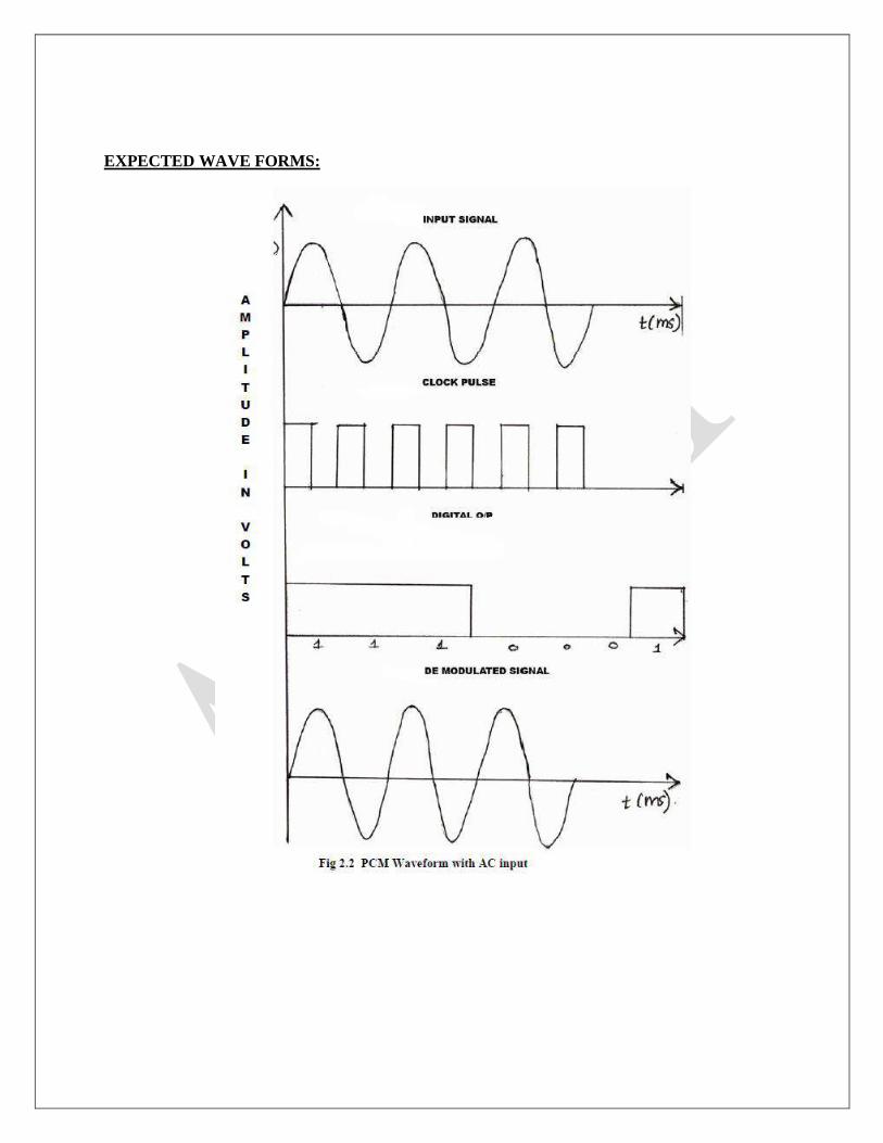
EXPECTED WAVE FORMS:
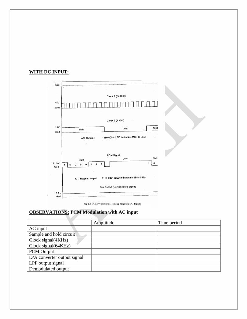
WITH DC INPUT:
OBSERVATIONS: PCM Modulation with AC input
Amplitude Time period
AC input
Sample and hold circuit
Clock signal(4KHz)
Clock signal(64KHz)
PCM Output
D/A converter output signal
LPF output signal
Demodulated output
PCM Modulation with DC input
Amplitude Time period
DC input
Clock signal(4KHz)
Clock signal(64KHz)
PCM Output
PCM Demodulated (with DC input)
Amplitude Time period
D/A converter output signal
LPF output signal
Demodulated output
RESULT:
Thus the Pulse Code modulation and demodulation were performed and graphs were plotted.
VIVA QUESTIONS:
1. What do you mean by quantizing process?
2. What will happen when sampling rate is greater than Nyquist rate ?
3. What will happen when sampling rate is less than Nyquist rate ?
4. Find the A/D Converter output for input DC voltage of 3.6V.
5. Fig shown below shows a PCM wave in which the amplitude levels of +1 volt and -1 volt are
used to represent binary symbols 1 and 0 respectively. The code word used consists of three bits.
Find the sampled version of an analog signal from which this PCM wave is derived.
6. Mention some applications of PCM.
7. What is the function of Sample and Hold circuit?
MATLAB CODE:
%% Pulse Code Modulation (PCM)
P=5; %percentage of errors in transmission
% sampling
t = [0:0.1:1*pi]; % Times at which to sample the sine function
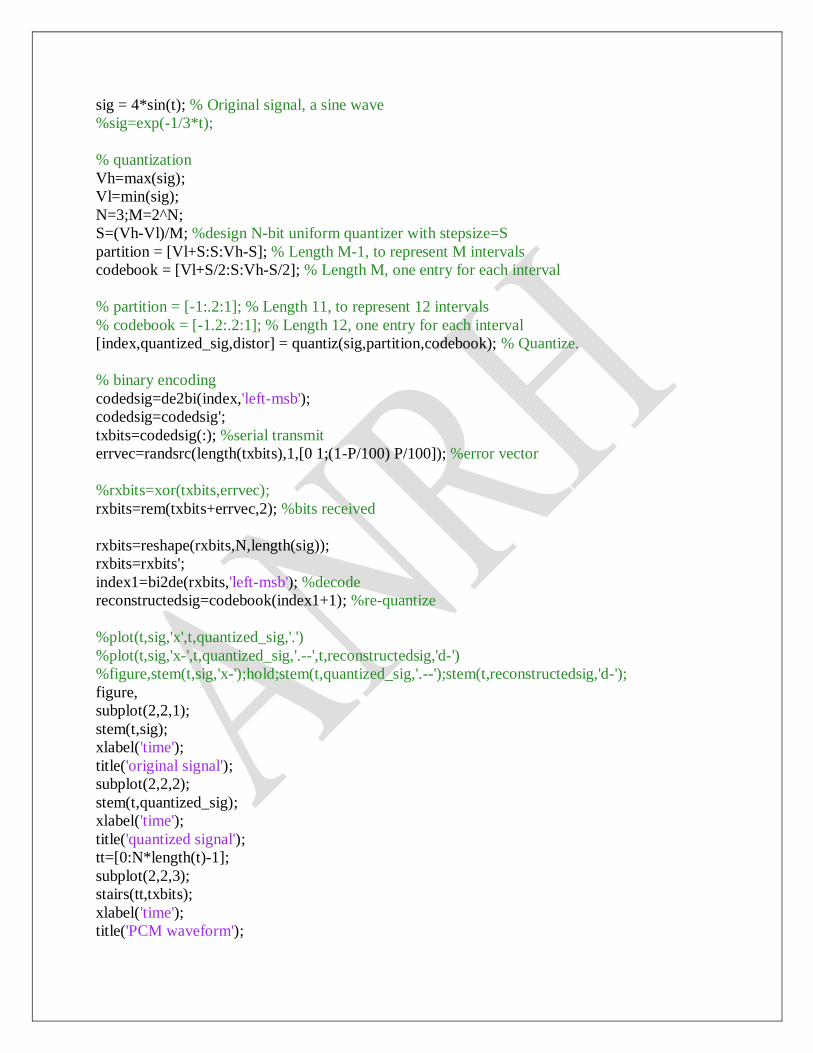
sig = 4*sin(t); % Original signal, a sine wave
%sig=exp(-1/3*t);
% quantization
Vh=max(sig);
Vl=min(sig);
N=3;M=2^N;
S=(Vh-Vl)/M; %design N-bit uniform quantizer with stepsize=S
partition = [Vl+S:S:Vh-S]; % Length M-1, to represent M intervals
codebook = [Vl+S/2:S:Vh-S/2]; % Length M, one entry for each interval
% partition = [-1:.2:1]; % Length 11, to represent 12 intervals
% codebook = [-1.2:.2:1]; % Length 12, one entry for each interval
[index,quantized_sig,distor] = quantiz(sig,partition,codebook); % Quantize.
% binary encoding
codedsig=de2bi(index,'left-msb');
codedsig=codedsig';
txbits=codedsig(:); %serial transmit
errvec=randsrc(length(txbits),1,[0 1;(1-P/100) P/100]); %error vector
%rxbits=xor(txbits,errvec);
rxbits=rem(txbits+errvec,2); %bits received
rxbits=reshape(rxbits,N,length(sig));
rxbits=rxbits';
index1=bi2de(rxbits,'left-msb'); %decode
reconstructedsig=codebook(index1+1); %re-quantize
%plot(t,sig,'x',t,quantized_sig,'.')
%plot(t,sig,'x-',t,quantized_sig,'.--',t,reconstructedsig,'d-')
%figure,stem(t,sig,'x-');hold;stem(t,quantized_sig,'.--');stem(t,reconstructedsig,'d-');
figure,
subplot(2,2,1);
stem(t,sig);
xlabel('time');
title('original signal');
subplot(2,2,2);
stem(t,quantized_sig);
xlabel('time');
title('quantized signal');
tt=[0:N*length(t)-1];
subplot(2,2,3);
stairs(tt,txbits);
xlabel('time');
title('PCM waveform');
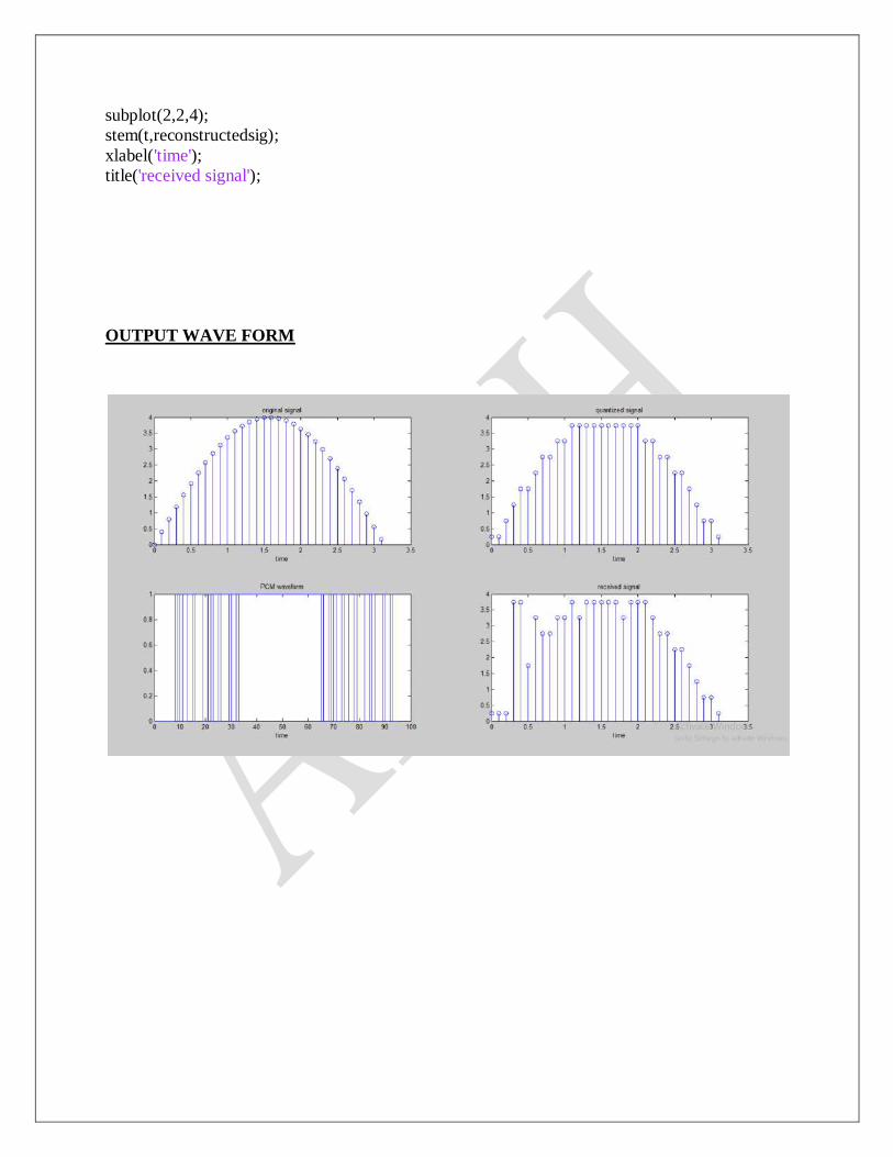
subplot(2,2,4);
stem(t,reconstructedsig);
xlabel('time');
title('received signal');
OUTPUT WAVE FORM
EXPERIMENT NO:10 DELTA MODULATION AND DEMODULATION
AIM:
To analyze a Delta modulation system. and interpret the modulated and demodulated waveforms
APPARATUS:
1. PCM Modulator trainer- AET-73M
2. PCM Demodulator trainer-AET-73D
3. C.R.O(30MHz)
4. Patch chords.
5. PC with windows(95/98/XP/NT/2000)
6. MATLAB Software with communication toolbox
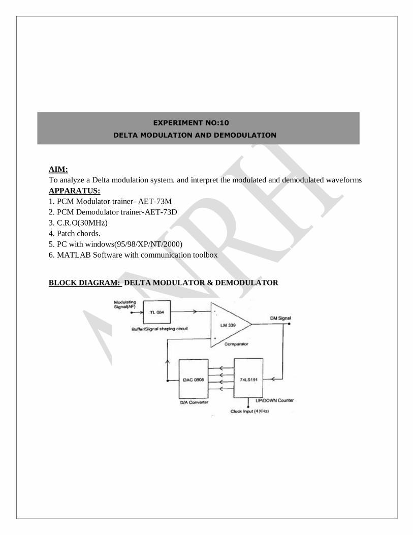
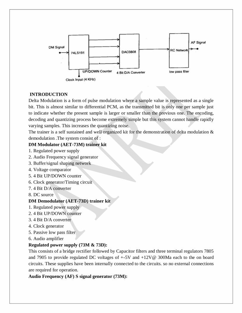
BLOCK DIAGRAM: DELTA MODULATOR & DEMODULATOR
INTRODUCTION
Delta Modulation is a form of pulse modulation where a sample value is represented as a single
bit. This is almost similar to differential PCM, as the transmitted bit is only one per sample just
to indicate whether the present sample is larger or smaller than the previous one. The encoding,
decoding and quantizing process become extremely simple but this system cannot handle rapidly
varying samples. This increases the quantizing noise.
The trainer is a self sustained and well organized kit for the demonstration of delta modulation &
demodulation .The system consist of :
DM Modulator (AET-73M) trainer kit
1. Regulated power supply
2. Audio Frequency signal generator
3. Buffer/signal shaping network
4. Voltage comparator
5. 4 Bit UP/DOWN counter
6. Clock generator/Timing circuit
7. 4 Bit D/A converter
8. DC source
DM Demodulator (AET-73D) trainer kit
1. Regulated power supply
2. 4 Bit UP/DOWN counter
3. 4 Bit D/A converter
4. Clock generator
5. Passive low pass filter
6. Audio amplifier
Regulated power supply (73M & 73D):
This consists of a bridge rectifier followed by Capacitor filters and three terminal regulators 7805
and 7905 to provide regulated DC voltages of +-5V and +12V@ 300Ma each to the on board
circuits. These supplies have been internally connected to the circuits. so no external connections
are required for operation.
Audio Frequency (AF) S signal generator (73M):
Sine wave signal of 100 Hz is generated to use as a modulating (message or information) signal
to be transmitted. This is an Op-Amp based Wein bridge Oscillators using IC TL084 is a
FET.input general purpose Operational Amplifier .Amplitude control is provided in the circuit to
vary the output amplitude of AF signal.
Clock generator/Timing circuit (73M & 73D):
A TTL compatible clock signal of 4 KHz frequency is provided on board to use as a clock to the
various circuits in the system. This circuit is a astable multivibrator using 555 timer followed by
a buffer.
DC Source (73M):
A 0 to +5V variable DC voltage is provided on board to use as a modulating signal instead of AF
Signal. is useful to study step by step operation of Delta modulation and Demodulation. This is a
simple circuit consists of potentiometer and fixed power supply.
Buffer/Signal shaping circuit (73M):
A non inverting buffer using IC TL 084 is provided at the input of the DM modulator followed
by a level shifting network. Buffer provides the isolation between DM circuit and the signal
source. Signal Shaping super imposes the 1.5V DC on incoming modulating signal so that the
input of the comparator lies between 0 and +3V maximum.
Voltage comparator (73D):
This circuit is build with IC LM339 The LM339 series consists of four independent precision
voltage comparators with an offset voltage specification as low as 2mV for all four comparators.
These were designed specifically to operate from a single power supply over a wide range of
voltages .Operation from split power supplies is also possible and the low power supply current
drain is independent of the magnitude of the power supply voltage. These comparators also have
a unique characteristic in that the common mode voltage range includes ground, even though
operated from a single power
supply voltage. Application areas include limit comparators simple analog to digital converters:
pulse, square and time delay generators. wide range VCO; MOS clock timers; multivibrators and
high voltage digital logic gates .The LM139 series was designed to directly interface with TTL
and CMOS. When operated from both plus and minus power supplies, they will directly interface
with MOS logic where the low power drain of the LM339 is a distinct advantage over standard
comparators .For circuit connections and other operating conditions.
Low pass filters (73D):
This is a series of simple RC networks provided on board to smoothen the output of the D/A
converter output. RC values are chosen such that the cutoff frequency would be at 100 Hz.
Amplifiers (73D):
This is an Op-amp (IC TL084) based non-inverting variable gain amplifiers provided on board to
amplify the recovered message singles i.e. output of low pass filter to desired level. Amplitude
control is provided in circuit to vary the gain of the amplifier between 0 and 6.AC/DC Switch
facilitates to couple the input signal through capacitor to directly to the amplifier input.
4 Bit UP/DOWN Counter (73M & 73 D):
This circuit is made using Synchronous 4-Bit Up/Down Counter with Mode Control IC 74LS191
.The DM 74LS191 circuit is a synchronous, reversible, counter. Synchronous operation is
provided by having all flip-flops clocked simultaneously. So that the outputs change
simultaneously when so instructed by the steering logic. This mode of operation eliminates the
output counting spikes normally associated with the asynchronous counters. The outputs of the
four master slave flip flops are triggered on a LOW to HIGH level transition of the clock input. if
the enable input is LOW a HIGH at the enable input inhibits counting .Level changes at either
the enable input or the down/up input should be made only when the clock input is HIGH. The
direction of the count is determined by the level of the down/up input. When LOW the counter
counts up and when HIGH it counts down. The counter is fully programmable that is the outputs
may be preset to either level by placing a LOW on the load input and entering the desired data at
the data inputs. The output will change independent of the level of the clock input. This feature
allows the counters to be used as modulo-N dividers by simply modifying the count length with
the preset inputs. The clock, down/up and load inputs are buffered to lower the drive requirement
which significantly reduces the number of clock drivers required for parallel words. The ripple
clock input produces a low level output pulse equal in width to the low level portion of the clock
input when an overflow or underflow condition exists. The counters can be easily cascaded by
feeding the ripple clock output to the enable input of the succeeding counter if parallel clocking
is used, or to the clock input if parallel enabling is used. The maximum/minimum count output
can be used to accomplish look-ahead for high speed operation.
4 Bit D/A converter (AET-73M & 73D):
This has been constructed with a popular 8 bit D/A Converter IC DAC 0808.The DAC0808 is an
8-bit monolithic DAC featuring a full scale output current settling time of 150 Ns while
dissipating only 33 maw with +-5V supplies. No reference current (I REF) trimming is required
for most applications since the full scale output current is typically +- 1 LSB of 255 I REF/256
.Relative accuracies of better than +- 0.19 % assure 8 bit monotonic and linearity while zero
level output current of less than 4 μA provides 8-bit zero accuracy for I REF [ greater than or
equal ] 2 math power supply currents of the DAC0808 is independent of bit codes, and exhibits
essentially constant device characteristics over the entire supply voltage range.4 LSB Bits are
permanently grounded
to make 4 bit converter. For complete specifications and operating conditions please refer the
data sheet of DAC0808.
DM Operation:
Figure 4.1 shows the basic block diagram of the PCM system. The modulating signal is applied
to buffer /signal shaping network. This applied signal will be superimposed by +1.5V DC so that
the negative portion the modulating signal will clamped to positive ,this process is needed
,because input of the comparator should be between 0 and +3V. After level shifting is done the
signal will be passed to inverting input of the comparator. on inverting input of the comparator is
connected to output of the 4 Bit D/A converter. Comparator is operating at +5V single supply
.So output of the comparator will be high (i.e. +vet Vast) when modulating signal is less than the
reference signal i.e. D/A output, otherwise it will be 0V. And this signal is transmitted as DM
signal .same signal is also connected as UP/DOWN control to the UP/DOWN counter (74LS
191). UP/DOWN counter is programmed for 0000 starting count. So initially output of the
counter is at 0000 and the D/A converter will be at 0V .Comparator compares the modulating
signal is greater than the reference signal. For next clock pulse depending on the UP/DOWN
input counter will count up or down. If the UP/DOWN input is low
(nothing but comparator output). Counter will make up and output will be 0001. So the D/A
converter will convert this 0001 digital input to equivalent analog signal(i.e. 0.3V 1 LSB
Value).Now the reference signal is 0.3V.If still modulating signal is greater than the D/A output
again comparator output(DM) will be low and UP count will occur. If not DOWN Count will
take place. This process will continue till the reference signal and modulating signal voltages are
equal. So DM signal is a series of 1 and 0. DM signal is applied to a UP/DOWN input of the
UP/DOWN counter at the receiver. This UP/DOWN counter is programmed for 1001 initial
value (i.e. power on reset) and mode control is activated. So depend on the UP/DOWN input for
the next clock pulse counter will count UP or DOWN. This output is applied to 4 Bit D/A
converter. A logic circuit is added to the counter which keeps the output of the counter in
between 0000 to 1111 always. Output of the D/A converter will be a staircase signal lies between
0 and +4.7V.This staircase signal is applied a low pass filter .This low pass will smoothen the
staircase signal so that original AF signal will be recovered. We can use a voltage amplifier at
the output of the low pass filter to amplify the recovered AF signal to desired voltage level.
PROCEDURE:
DM Modulator:
1. Study the theory of operation
2. Connect the trainer (AET-73M) -
3. Observe the output of AF generator using CRO; it should be a Sine wave of 100 Hz frequency
with 3Vpp amplitude.
4. Verify the output of the DC source with multimeter/scope; output should vary 0 to +4V
5. Observe the output of the clock generator using Crotchety should be 4 KHz frequency of
square wave with 5 Up amplitude.
Note: This clock signal is internally connected to the up/down counter so no external connection
is required.
DM With DC Voltage as modulating signal:
6. Connect DC signal from the DC source to the inverting input of the comparator and set some
voltage says 3V.
7. Observe and plot the signals at D/A converter output (i.e. non-inverting input of the
comparator), DM signal using CRO and compare them with the waveforms given in figure.
8. Connect DM signal (from 73M) to the DM input of the demodulator.
9. Connect clock (4KHz) from modulator (73M) to the clock input of the demodulator (73D).
Connect clock input of UP/DOWN counter (in 73D) to the clock from transmitter with the help
of springs provided.
10. Observe digital output (LED indication) of the UP/DOWN counter (in 73 D) and compare it
with the output of the UP/DOWN (in 73M) .By this you can notice that the both the outputs are
same.
11. Observe and plot the output of the D/A converter and compare it with the waveforms given
in figure.
12. Measure the demodulated signal (i.e. output of the D/A converter 73D with the help of
multimeter and compare it with the original signal 73 M. From the above observation you can
notice that both the voltages are equal and there is no loss in process of modulation, transmission
and demodulation.
13. Similarly you can verify the DM operation for different values of modulating signal.
DM With AF Voltage as modulating signal:
14. Connect AF signal from the AF source to the inverting input of the comparator and set ome
voltage says 3V.
15. Observe and plot the signals at D/A converter output (i.e. non-inverting input of the
comparator), DM signal using CRO and compare them with the waveforms given in figure.
16. Connect DM signal (from 73M) to the DM input of the demodulator.
17. Connect clock (4KHz) from modulator (73M) to the clock input of the demodulator (73D).
18. Connect clock input of UP/DOWN counter (in 73D) to the clock from transmitter with the
help of springs provided.
19. Observe and plot the output of the D/A converter and compare it with the waveforms given
in figure.
20. Observe and sketch the D/A output.
21. Connect D/A output to the LPF input.
22. Observe the output of the LPF/Amplifier and compare it with the original modulating signal
(AET-73M).
23. From the above observation you can verify that there is no loss in information in conversion
and transmission process.
24. Disconnect clock from transmitter (AET-73M) and connect to local oscillator (i.e. clock
generator output from AET-73D) with remaining setup as it is. Observe demodulated signal
output and compare it with the previous result. This signal is little bit distorted in shape. This is
because lack of synchronization between clock at transmitter and clock at receiver.
Note: you can take modulating signals from external sources. Maximum amplitude should not
exceed 4 V in case of DC and 3 Vpp in case of AC (AF) signals.
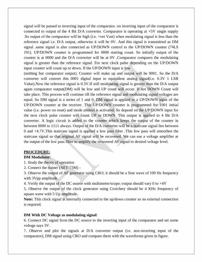
EXPECTED WAVE FORMS: FOR AC INPUT
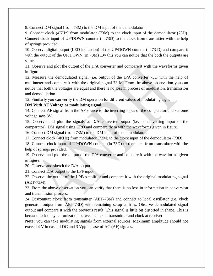
FOR DC INPUT
OBSERVATIONS: DM MODULATION WITH AC INPUT
amplitude Time period
AC input
D/A converter output
Clock signal (4 KHz)
DM output
DM DEMODULATION WITH AC INPUT
amplitude Time period
DM input
D/A converter output signal
Demodulated Output
Clock signal (4 KHz)
DM MODULATION WITH DC INPUT
amplitude Time period
DC input
D/A converter output
Clock signal (4 KHz)
DM output
DM DEMODULATION WITH DC INPUT
amplitude Time period
DM input
D/A converter output signal
Demodulated Output
Clock signal (4 KHz)
RESULT:
Thus the Delta modulation and demodulation were performed and graphs were
plotted.
VIVA QUESTIONS:
1. Compare DPCM ,PCM& Delta modulation.
2. How to reduce the quantization noise that occurs in DM?
3. A band pass signal has a spectral range that extends from 20 to 82 KHz.Find the acceptable
sampling frequency.
4. Find the fourier series expansion of an Impulse train.
5. Mention the applications of DM.
MATLAB CODE:
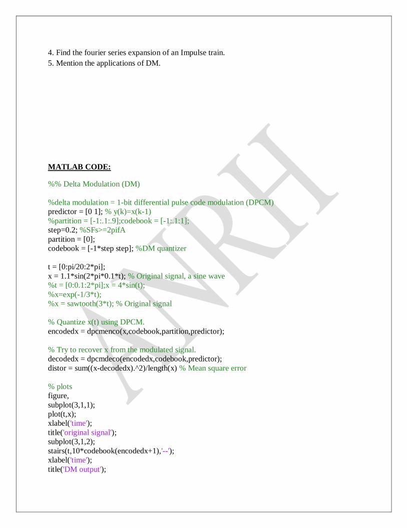
%% Delta Modulation (DM)
%delta modulation = 1-bit differential pulse code modulation (DPCM)
predictor = [0 1]; % y(k)=x(k-1)
%partition = [-1:.1:.9];codebook = [-1:.1:1];
step=0.2; %SFs>=2pifA
partition = [0];
codebook = [-1*step step]; %DM quantizer
t = [0:pi/20:2*pi];
x = 1.1*sin(2*pi*0.1*t); % Original signal, a sine wave
%t = [0:0.1:2*pi];x = 4*sin(t);
%x=exp(-1/3*t);
%x = sawtooth(3*t); % Original signal
% Quantize x(t) using DPCM.
encodedx = dpcmenco(x,codebook,partition,predictor);
% Try to recover x from the modulated signal.
decodedx = dpcmdeco(encodedx,codebook,predictor);
distor = sum((x-decodedx).^2)/length(x) % Mean square error
% plots
figure,
subplot(3,1,1);
plot(t,x);
xlabel('time');
title('original signal');
subplot(3,1,2);
stairs(t,10*codebook(encodedx+1),'--');
xlabel('time');
title('DM output');
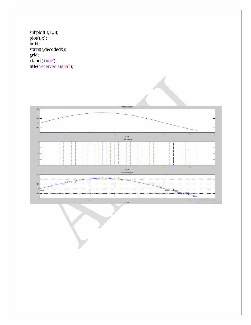
subplot(3,1,3);
plot(t,x);
hold;
stairs(t,decodedx);
grid;
xlabel('time');
title('received signal');
EXPERIMENT NO: 11
FSK- GENERATION AND DETECTION
AIM:
To analyze a FSK modulation system. And interpret the modulated and demodulated waveforms
APPRATUS:
1. FSK Trainer Kit - AET-48
2. Dual Trace oscilloscope
3. Digital Multimeter
4. C.R.O(30MHz)
5. Patch chords.
6. PC with windows(95/98/XP/NT/2000)
7. MATLAB Software with communication toolbox
BLOCK DIAGRAM:
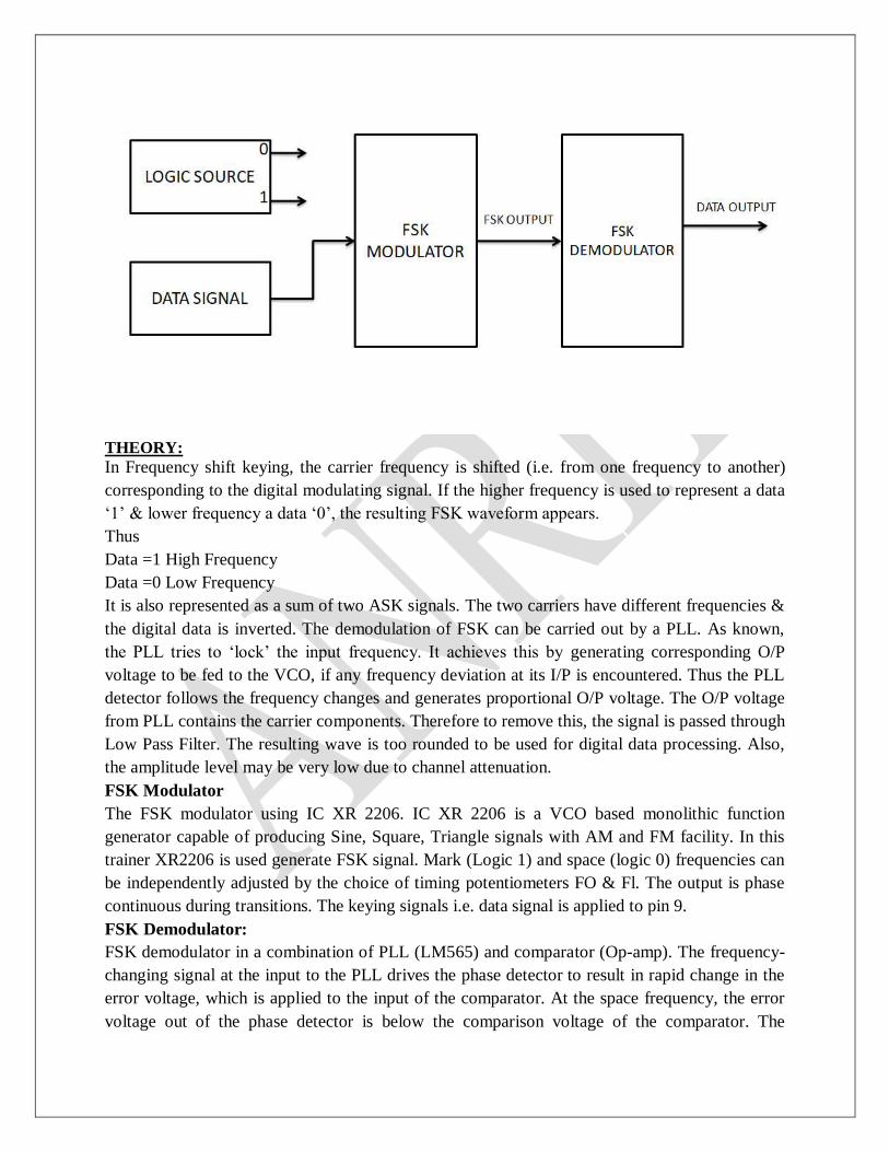
THEORY:
In Frequency shift keying, the carrier frequency is shifted (i.e. from one frequency to another)
corresponding to the digital modulating signal. If the higher frequency is used to represent a data
‘1’ & lower frequency a data ‘0’, the resulting FSK waveform appears.
Thus
Data =1 High Frequency
Data =0 Low Frequency
It is also represented as a sum of two ASK signals. The two carriers have different frequencies &
the digital data is inverted. The demodulation of FSK can be carried out by a PLL. As known,
the PLL tries to ‘lock’ the input frequency. It achieves this by generating corresponding O/P
voltage to be fed to the VCO, if any frequency deviation at its I/P is encountered. Thus the PLL
detector follows the frequency changes and generates proportional O/P voltage. The O/P voltage
from PLL contains the carrier components. Therefore to remove this, the signal is passed through
Low Pass Filter. The resulting wave is too rounded to be used for digital data processing. Also,
the amplitude level may be very low due to channel attenuation.
FSK Modulator
The FSK modulator using IC XR 2206. IC XR 2206 is a VCO based monolithic function
generator capable of producing Sine, Square, Triangle signals with AM and FM facility. In this
trainer XR2206 is used generate FSK signal. Mark (Logic 1) and space (logic 0) frequencies can
be independently adjusted by the choice of timing potentiometers FO & Fl. The output is phase
continuous during transitions. The keying signals i.e. data signal is applied to pin 9.
FSK Demodulator:
FSK demodulator in a combination of PLL (LM565) and comparator (Op-amp). The frequency-
changing signal at the input to the PLL drives the phase detector to result in rapid change in the
error voltage, which is applied to the input of the comparator. At the space frequency, the error
voltage out of the phase detector is below the comparison voltage of the comparator. The
comparator is a non-inverting circuit, so its output level is also low. As the phase detector input
frequency shifts low (to the mark frequency), the error voltage steps to a high level, passing
through the comparison level, causing the comparator output voltage to go high. This error
voltage change will snap the comparator output voltage between its two output levels in manner
that duplicates the data signal input to the XR22OS modulator. The free running frequency of the
PLL (no input signal) is set midway between the mark and space frequencies. A space at 2025
Hz and mark at 2225 Hz will have a free running VCO frequency of 2125 Hz.
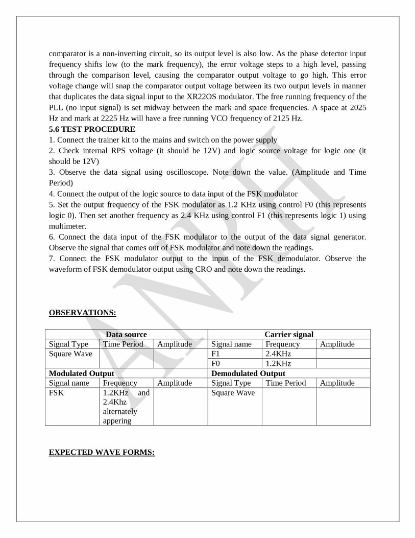
5.6 TEST PROCEDURE
1. Connect the trainer kit to the mains and switch on the power supply
2. Check internal RPS voltage (it should be 12V) and logic source voltage for logic one (it
should be 12V)
3. Observe the data signal using oscilloscope. Note down the value. (Amplitude and Time
Period)
4. Connect the output of the logic source to data input of the FSK modulator
5. Set the output frequency of the FSK modulator as 1.2 KHz using control F0 (this represents
logic 0). Then set another frequency as 2.4 KHz using control F1 (this represents logic 1) using
multimeter.
6. Connect the data input of the FSK modulator to the output of the data signal generator.
Observe the signal that comes out of FSK modulator and note down the readings.
7. Connect the FSK modulator output to the input of the FSK demodulator. Observe the
waveform of FSK demodulator output using CRO and note down the readings.
OBSERVATIONS:
Data source Carrier signal
Signal Type Time Period Amplitude Signal name Frequency Amplitude
Square Wave
F1 2.4KHz
F0 1.2KHz
Modulated Output Demodulated Output
Signal name Frequency Amplitude Signal Type Time Period Amplitude
FSK 1.2KHz and
2.4Khz
alternately
appering
Square Wave
EXPECTED WAVE FORMS:
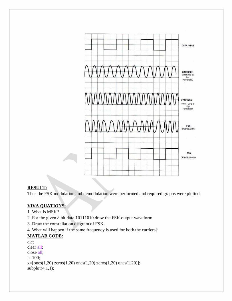
RESULT:
Thus the FSK modulation and demodulation were performed and required graphs were plotted.
VIVA QUATIONS:
1. What is MSK?
2. For the given 8 bit data 10111010 draw the FSK output waveform.
3. Draw the constellation diagram of FSK.
4. What will happen if the same frequency is used for both the carriers?
MATLAB CODE:
clc;
clear all;
close all;
n=100;
x=[ones(1,20) zeros(1,20) ones(1,20) zeros(1,20) ones(1,20)];
subplot(4,1,1);
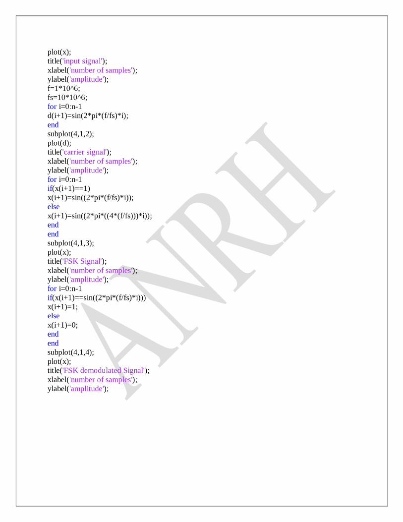
plot(x);
title('input signal');
xlabel('number of samples');
ylabel('amplitude');
f=1*10^6;
fs=10*10^6;
for i=0:n-1
d(i+1)=sin(2*pi*(f/fs)*i);
end
subplot(4,1,2);
plot(d);
title('carrier signal');
xlabel('number of samples');
ylabel('amplitude');
for i=0:n-1
if(x(i+1)==1)
x(i+1)=sin((2*pi*(f/fs)*i));
else
x(i+1)=sin((2*pi*((4*(f/fs)))*i));
end
end
subplot(4,1,3);
plot(x);
title('FSK Signal');
xlabel('number of samples');
ylabel('amplitude');
for i=0:n-1
if(x(i+1)==sin((2*pi*(f/fs)*i)))
x(i+1)=1;
else
x(i+1)=0;
end
end
subplot(4,1,4);
plot(x);
title('FSK demodulated Signal');
xlabel('number of samples');
ylabel('amplitude');
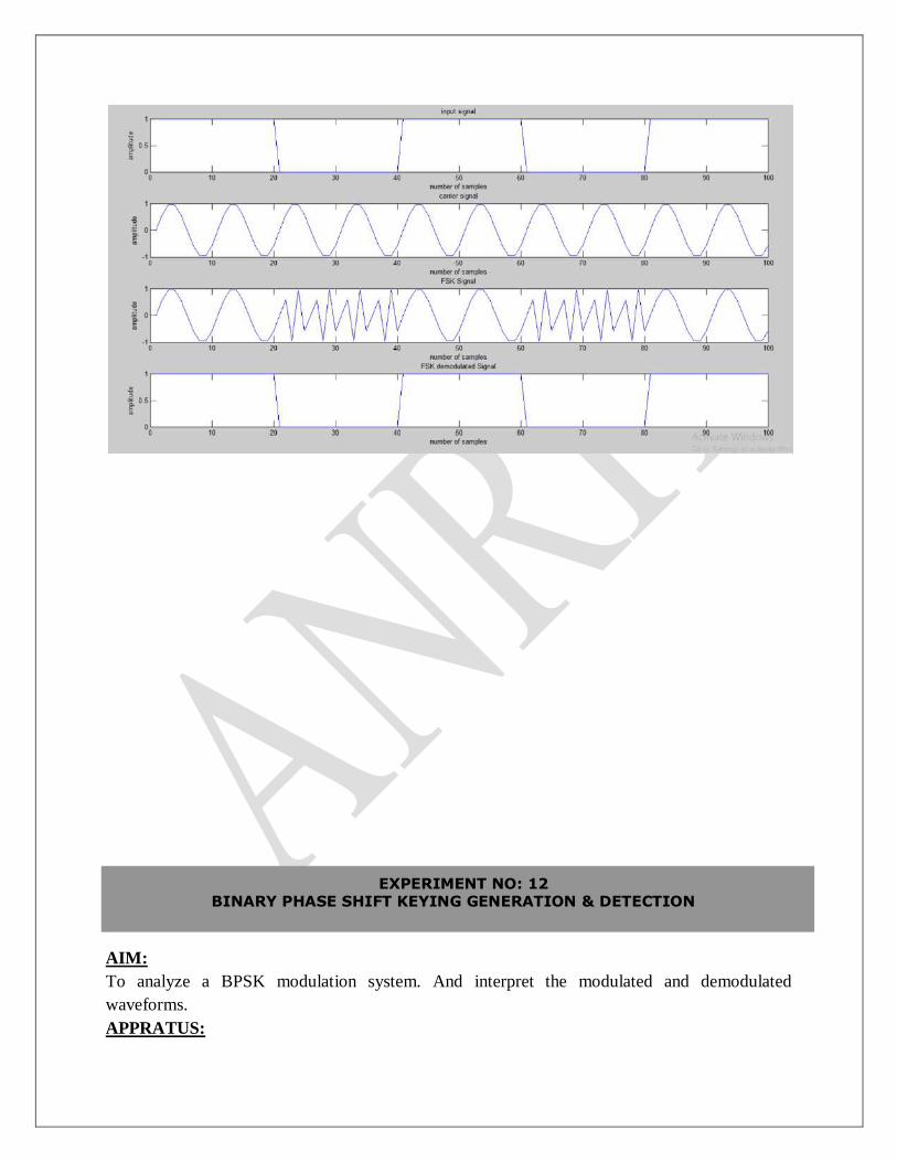
EXPERIMENT NO: 12 BINARY PHASE SHIFT KEYING GENERATION & DETECTION
AIM:
To analyze a BPSK modulation system. And interpret the modulated and demodulated
waveforms.
APPRATUS:
1. BPSK Trainer Kit - AET-48
2. Dual Trace oscilloscope
3. Digital Multimeter
4. C.R.O(30MHz)
5. Patch chords.
6. PC with windows(95/98/XP/NT/2000)
7. MATLAB Software with communication toolbox
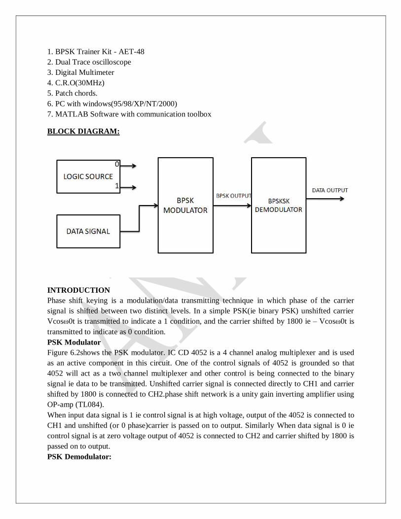
BLOCK DIAGRAM:
INTRODUCTION
Phase shift keying is a modulation/data transmitting technique in which phase of the carrier
signal is shifted between two distinct levels. In a simple PSK(ie binary PSK) unshifted carrier
Vcosω0t is transmitted to indicate a 1 condition, and the carrier shifted by 1800 ie – Vcosω0t is
transmitted to indicate as 0 condition.
PSK Modulator
Figure 6.2shows the PSK modulator. IC CD 4052 is a 4 channel analog multiplexer and is used
as an active component in this circuit. One of the control signals of 4052 is grounded so that
4052 will act as a two channel multiplexer and other control is being connected to the binary
signal ie data to be transmitted. Unshifted carrier signal is connected directly to CH1 and carrier
shifted by 1800 is connected to CH2.phase shift network is a unity gain inverting amplifier using
OP-amp (TL084).
When input data signal is 1 ie control signal is at high voltage, output of the 4052 is connected to
CH1 and unshifted (or 0 phase)carrier is passed on to output. Similarly When data signal is 0 ie
control signal is at zero voltage output of 4052 is connected to CH2 and carrier shifted by 1800 is
passed on to output.
PSK Demodulator:
Demodulation of PSK is achieved by subtracting the received carrier from a derived synchronous
reference carrier of constant phase. Figure shows the simple coherent(synchronous) PSK
modulator. Received PSK signal is converted to square wave using an op-amp(TL084) based
zero crossing detector and connected to EX-OR circuit. The derived reference carrier is
connected to other input of the EX-OR Gate through an op-amp based zero crossing detector. For
the simplicity same carrier is used at receiver as reference carrier (In practical communication
system reference carrier is generated at receiver).We can observe the exact operation of
demodulator with the help of waveforms at various nodes in the circuit. Received PSK signal is
converted to square wave using an op-amp(TL084) based zero crossing detector and connected
to EX-OR circuit. The derived reference carrier is connected to other input of the EX-OR Gate
through an op-amp based zero crossing
detector. For the simplicity same carrier is used at receiver as reference carrier (In practical
communication system reference carrier is generated at receiver).We can observe the exact
operation of demodulator with the help of waveforms at various nodes in the circuit.
THOERY:
10.5 THEORY
Binary Phase Shift Keying
In a coherent binary PSK system, the pair of signal S1(t) and S2 (t) used to represent binary
symbols 1 & 0 are defined by
S1 (t) = √2Eb/τb Cos 2πfct
S2 (t) =√2Eb/Tb (2πfct+π) = - √ 2Eb/Tb Cos 2πfct where 0 ≤ t< Tb and
Eb = Transmitted signed energy for bit
The carrier frequency fc =n/Tb for some fixed integer n.
In BPSK, there is only one basis function of unit energy.
Øb (t) = √2/Tb cos 2fπct 0≤ t< Tb
S1 (t) = √Eb Ø1 (t) 0≤ t ≤Tb
S2 (t) = √Eb Ø1 (t) 0≤ t< Tb
The signal space is 1dimensional (N=1) having two message points (M = 2)
Block Diagram of BPSK Transmitter
The input binary symbols are represented in polar form with symbols 1 & 0 represented by
constant amplitude levels √Eb & -√Eb. This binary wave is multiplied by a sinusoidal carrier in a
product modulator. The result in a BSPK signal.
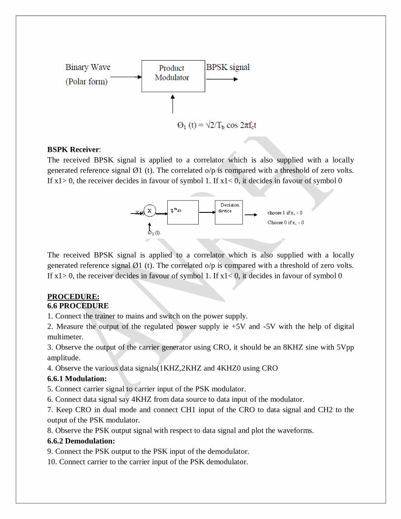
BSPK Receiver:
The received BPSK signal is applied to a correlator which is also supplied with a locally
generated reference signal Ø1 (t). The correlated o/p is compared with a threshold of zero volts.
If x1> 0, the receiver decides in favour of symbol 1. If x1< 0, it decides in favour of symbol 0
The received BPSK signal is applied to a correlator which is also supplied with a locally
generated reference signal Ø1 (t). The correlated o/p is compared with a threshold of zero volts.
If x1> 0, the receiver decides in favour of symbol 1. If x1< 0, it decides in favour of symbol 0
PROCEDURE:
6.6 PROCEDURE
1. Connect the trainer to mains and switch on the power supply.
2. Measure the output of the regulated power supply ie +5V and -5V with the help of digital
multimeter.
3. Observe the output of the carrier generator using CRO, it should be an 8KHZ sine with 5Vpp
amplitude.
4. Observe the various data signals(1KHZ,2KHZ and 4KHZ0 using CRO
6.6.1 Modulation:
5. Connect carrier signal to carrier input of the PSK modulator.
6. Connect data signal say 4KHZ from data source to data input of the modulator.
7. Keep CRO in dual mode and connect CH1 input of the CRO to data signal and CH2 to the
output of the PSK modulator.
8. Observe the PSK output signal with respect to data signal and plot the waveforms.
6.6.2 Demodulation:
9. Connect the PSK output to the PSK input of the demodulator.
10. Connect carrier to the carrier input of the PSK demodulator.
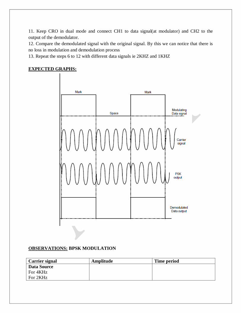
11. Keep CRO in dual mode and connect CH1 to data signal(at modulator) and CH2 to the
output of the demodulator.
12. Compare the demodulated signal with the original signal. By this we can notice that there is
no loss in modulation and demodulation process
13. Repeat the steps 6 to 12 with different data signals ie 2KHZ and 1KHZ
EXPECTED GRAPHS:
OBSERVATIONS: BPSK MODULATION
Carrier signal Amplitude Time period
Data Source
For 4KHz
For 2KHz
For 1KHz
Modulated Output
For 4KHz
For 2KHz
For 1KHz
BPSK DEMODULATION
Amplitude Time period
Demodulated Output
For 4KHz
For 2KHz
For 1KHz
RESULT:
Thus the PSK modulation and demodulation were performed and graphs were plotted.
VIVA QUESTIONS:
1. Compare FSK and PSK.
2. List the Characteristics of TL084 op-amp.
3. Compare TL084 op amp with IC 741 op amp.
4. What do we infer from constellation diagrams of various modulation schemes?
MATLAB CODE:
clc;
clear all;
close all;
n=100;
x=[ones(1,20) zeros(1,20) ones(1,20) zeros(1,20) ones(1,20)];
subplot(4,1,1);
plot(x);
title('input signal');
xlabel('number of samples');
ylabel('amplitude');
f=1*10^6;
fs=10*10^6;
for i=0:n-1
d(i+1)=sin(2*pi*(f/fs)*i);
end
subplot(4,1,2);
plot(d);
title('carrier signal');
xlabel('number of samples');
ylabel('amplitude');
for i=0:n-1
if(x(i+1)==0)
x(i+1)=sin(2*pi*(f/fs)*i);
else
x(i+1)=sin(2*pi*(f/fs)*i+pi);
end
end
subplot(4,1,3);
plot(x);
title('BPSK Signal');
xlabel('number of samples');
ylabel('amplitude');
for i=0:n-1
if(x(i+1)==sin(2*pi*(f/fs)*i))
x(i+1)=0;
else
x(i+1)=1;
end
end
subplot(4,1,4);
plot(x);
title('Demodulated Signal');
xlabel('number of samples');
ylabel('amplitude');
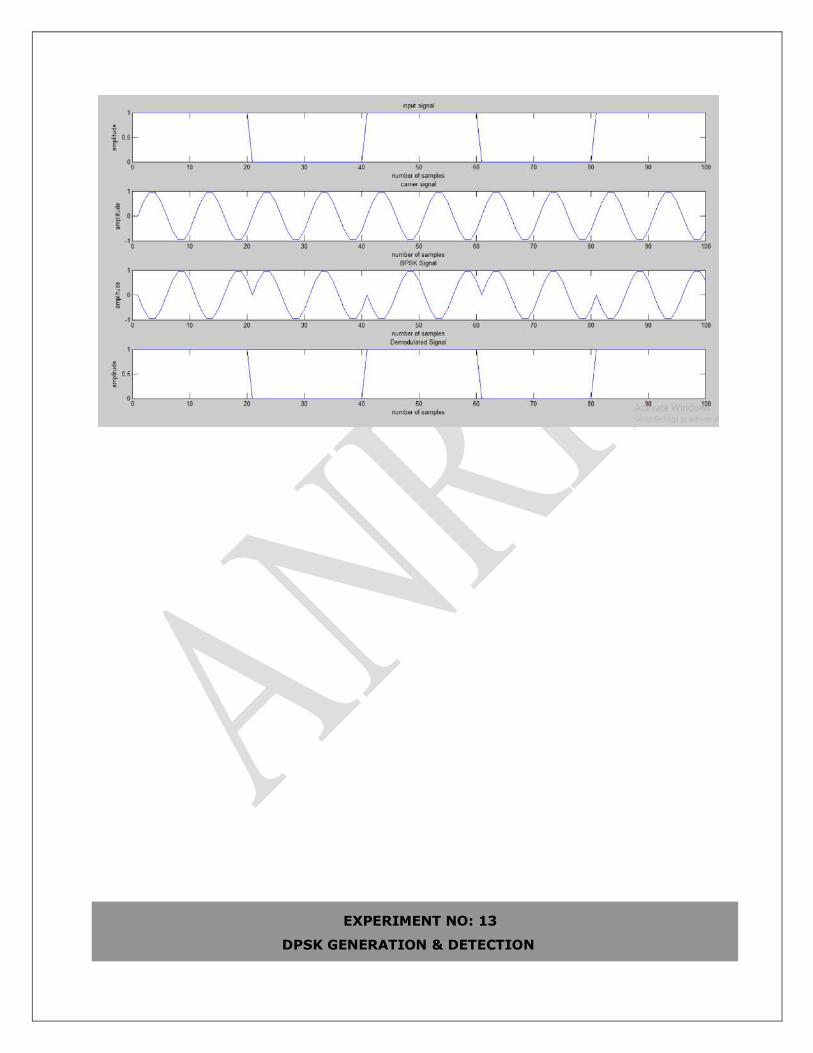
EXPERIMENT NO: 13 DPSK GENERATION & DETECTION
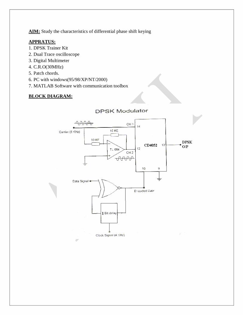
AIM: Study the characteristics of differential phase shift keying
APPRATUS:
1. DPSK Trainer Kit
2. Dual Trace oscilloscope
3. Digital Multimeter
4. C.R.O(30MHz)
5. Patch chords.
6. PC with windows(95/98/XP/NT/2000)
7. MATLAB Software with communication toolbox
BLOCK DIAGRAM:
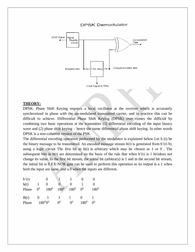
THEORY:
DPSK: Phase Shift Keying requires a local oscillator at the receiver which is accurately
synchronized in phase with the un-modulated transmitted carrier, and in practice this can be
difficult to achieve. Differential Phase Shift Keying (DPSK) over comes the difficult by
combining two basic operations at the transmitter (1) differential encoding of the input binary
wave and (2) phase shift keying – hence the name differential phase shift keying. In other words
DPSK is a non-coherent version of the PSK.
The differential encoding operation performed by the modulator is explained below Let b (t) be
the binary message to be transmitted. An encoded message stream b(t) is generated from b’(t) by
using a logic circuit The first bit in b(t) is arbitrary which may be chosen as 1 or 0 . The
subsequent bits in b(t) are determined on the basis of the rule that when b’(t) is 1 b(t)does not
change its value. In the first bit stream, the initial bit (arbitrary) is 1 and in the second bit stream,
the initial bit is 0 EX-NOR gate can be used to perform this operation as its output is a 1 when
both the input are same, and a 0 when the inputs are different.
b’(t) 0 1 1 0 0
b(t) 1 0 0 0 1 0
Phase 00 1800 1800 1800 00 1800
B(t) 0 1 1 1 0 1
Phase 1800 00 00 00 1800 00
Example for Complete DPSK operation (with arbitrary bit as 0):
Message signal (to be transmitted) 0 1 1 0 0
Encoded data (differential data) 0 1 1 1 0 1
Transmitted signal phase: 1800 00 00 00 1800 00
Received signal phase: 1800 00 00 00 1800 00
Encoded data (differential data) 0 1 1 1 0
Message signal (Demodulation) 0 1 1 0 0
DPSK Demodulator:
DPSK Modulator: IC CD 4052 is a 4 channel analog multiplexer and is used as an active
component in this circuit. One of the control signals of 4052 is grounded so that 4052 will act as
a two channel multiplexer and other control is being connected to the binary signal i.e., encoded
data. Un- shifted carrier signal is connected directly to CH1 and carrier shifted by 1800is
connected to CH2. Phase shift network is a unity gain inverting amplifier using Op-Amp
(TL084).
When control signal is at high voltage, output of the 4052 is connected to CH1 and un-shifted (or
0 phase) carrier is passed on to output. Similarly when control signal is at zero voltage output of
4052 is connected to CH2 and carrier shifted by 1800 is passed on to output.
Differential encoder: This consists of 1 bit delay circuit and an X-NOR Gate. 1 bit delay circuit
is formed by a D-Latch. Data signal i.e., signal to be transmitted is connected to one of the input
of the X-NOR gate and other one being connected to out of the delay circuit. Output of the
X-NOR gate and is connected to control input of the multiplexer (IC 4052) and as well as to
input of the D-Latch. Output of the X-NOR gate is 1 when both the inputs are same and it is 0
when both the inputs are different.
DPSK Demodulator: This consists of 1 bit delay circuit, X-NOR Gate and a signal shaping
circuit. Signal shaping circuit consists of Op-amp based zero crossing detector followed by a
D-latch. Receiver DPSK signal is converted to square wave with the help of zero crossing and
this square wave will pass through the D-Latch. So output of the D-latch is an encoded data. This
encoded data is applied to 1 bit delay circuit as well as to one of the inputs of X-NOR gate. And
output of the delay circuit is connected to another input of the X-NOR gate. Output of the
X-NOR gate is 1 when both the inputs are same and it is 0 when both the inputs are different.
PROCEDURE: MODULATOR
1. Connect carrier signal to carrier input of the PSK Modulator.
2. Connect data signal from data input of the X-NOR gate.
3. Keep CRO in dual mode.
4. Connect CH1 input of the CRO to data signal and CH2 input to the encoded data (which is
nothing but the output of the X-NOR gate)
5. Observe the encoded data with respect to data input. The encoded data will be in a given
sequence.
6. Actual data signal : 10101101001010110100
7. Encoded data signal : 01100011011001110010
8. Now connect CH2 input of the CRO to the DPSK output and CH1 input to the encoded data.
Observe the input and output waveforms and plot the same.
9. Compare the plotted waveforms with the given waveforms in fig: 1.3
10. Note: Observe and plot the waveforms after perfect triggering. Better to keep the encoded
data more than 4 cycles for perfect triggering.
DEMODULATOR
1. Connect DPSK signal to the input of the signal shaping circuit from DPSK transmitter with
the help of coaxial cable (supplied with trainer).
2. Connect clock from the transmitter (i.e. DPSK Modulator) to clock input of the 1 bit delay
circuit using coaxial cable.
3. Keep CRO in dual mode. Connect CH1 input to the encoded data (at modulator) and CH2
input to the encoded data (at demodulator).
4. Observe and plot both the waveforms and compare it with the given waveforms. You will
notice that both the signals are same with one bit delay.
5. Keep CRO in dual mode. Connect CH1 input to the data signal (at modulator) and CH2 input
to the output of the demodulator.
6. Observe and plot both the waveforms and compare it with the given waveforms. You will
notice that both the signals are same with one bit delay.
7. Disconnect clock from transmitter and connect to local oscillator clock (i.e., clock generator
output from De Modulator) with remaining setup as it is. Observe demodulator output and
compare it with the previous output. This signal is little bit distorted. This is because lack of
synchronization between clock at modulator and clock at demodulator. You can get further
perfection in output waveform by adjusting the locally generated clock frequency by varying
potentiometer.
EXPECTED WAVEFORMS:
RESULT:
Thus the DPSK modulation and demodulation were performed and graphs were plotted.
VIVA QUESTIONS:
1. Define DPSK?
2. Mention the Advantages of DPSK?
3. Mention the Disadvantages of DPSK?
4. Draw the waveforms of DPSK?
5. Compare ASK, PSK, FSK& DPSK?
6. What are the Applications of DPSK?
7. What is the expression for DPSK Error?
8. Why do we need 1-Bit delay in DPSK Modulator & Demodulator?
9. How does DPSK differ from PSK?
10. Is the error rate of DPSK is greater than PSK?
MATLAB CODE:
N = 10^4 % number of bits or symbols
rand('state',100); % initializing the rand() function
randn('state',200);% initializing the randn() function
ip = rand(1,N)>0.5;% generating 0,1 with equal probability
ipD = mod(filter(1,[1 -1],ip),2); % %differential encoding y[n]=y[n-1]+x[n]
s = 2*ipD-1; % BPSK modulation 0 -> -1; 1 -> 0
n = 1/sqrt(2)*[randn(1,N) + j*randn(1,N)]; % white gaussian noise, 0dB variance
Eb_N0_dB = [-3:10]; % multiple Eb/N0 values
for ii = 1:length(Eb_N0_dB)
y = s + 10^(-Eb_N0_dB(ii)/20)*n; % additive white gaussian noise
ipDHat_coh = real(y) > 0; % coherent demodulation
ipHat_coh = mod(filter([1 -1],1,ipDHat_coh),2); %differential decoding
nErr_dbpsk_coh(ii) = size(find([ip - ipHat_coh]),2); % counting the number of errors
end
simBer_dbpsk_coh = nErr_dbpsk_coh/N;
theoryBer_dbpsk_coh = erfc(sqrt(10.^(Eb_N0_dB/10))).*(1 -
.5*erfc(sqrt(10.^(Eb_N0_dB/10))));
close all
figure
semilogy(Eb_N0_dB,theoryBer_dbpsk_coh,'b.-');
hold on
semilogy(Eb_N0_dB,simBer_dbpsk_coh,'mx-');
axis([-2 10 10^-6 0.5])
grid on
legend('theory', 'simulation');
xlabel('Eb/No, dB')
ylabel('Bit Error Rate')
title('Bit error probability curve for coherent demodulation of DBPSK')
EXPERIMENT NO: 14
QPSK GENERATION & DETECTION
AIM: To study modulation and demodulation of QPSK and sketch the relevant waveforms.
APPRATUS:
1. QPSK Trainer Kit
2. Dual Trace oscilloscope
3. Digital Multimeter
4. C.R.O(30MHz)
5. Patch chords.
6. PC with windows(95/98/XP/NT/2000)
7. MATLAB Software with communication toolbox
BLOCK DIAGRAM: QPSK MODULATOR & DEMODULATOR
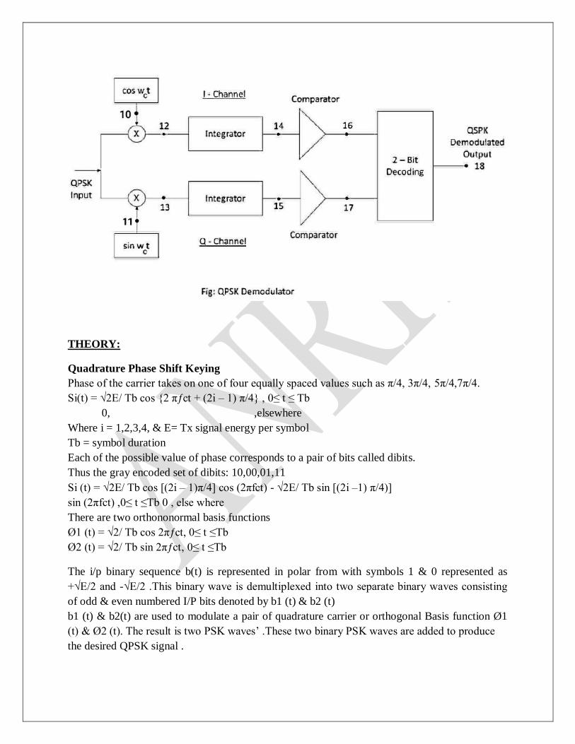
THEORY:
Quadrature Phase Shift Keying
Phase of the carrier takes on one of four equally spaced values such as π/4, 3π/4, 5π/4,7π/4.
Si(t) = √2E/ Tb cos {2 πƒct + (2i – 1) π/4} , 0≤ t ≤ Tb
0, ,elsewhere
Where i = 1,2,3,4, & E= Tx signal energy per symbol
Tb = symbol duration
Each of the possible value of phase corresponds to a pair of bits called dibits.
Thus the gray encoded set of dibits: 10,00,01,11
Si (t) = √2E/ Tb cos [(2i – 1)π/4] cos (2πfct) - √2E/ Tb sin [(2i –1) π/4)]
sin (2πfct) ,0≤ t ≤Tb 0 , else where
There are two orthononormal basis functions
Ø1 (t) = √2/ Tb cos 2πƒct, 0≤ t ≤Tb
Ø2 (t) = √2/ Tb sin 2πƒct, 0≤ t ≤Tb
The i/p binary sequence b(t) is represented in polar from with symbols 1 & 0 represented as
+√E/2 and -√E/2 .This binary wave is demultiplexed into two separate binary waves consisting
of odd & even numbered I/P bits denoted by b1 (t) & b2 (t)
b1 (t) & b2(t) are used to modulate a pair of quadrature carrier or orthogonal Basis function Ø1
(t) & Ø2 (t). The result is two PSK waves’ .These two binary PSK waves are added to produce
the desired QPSK signal .
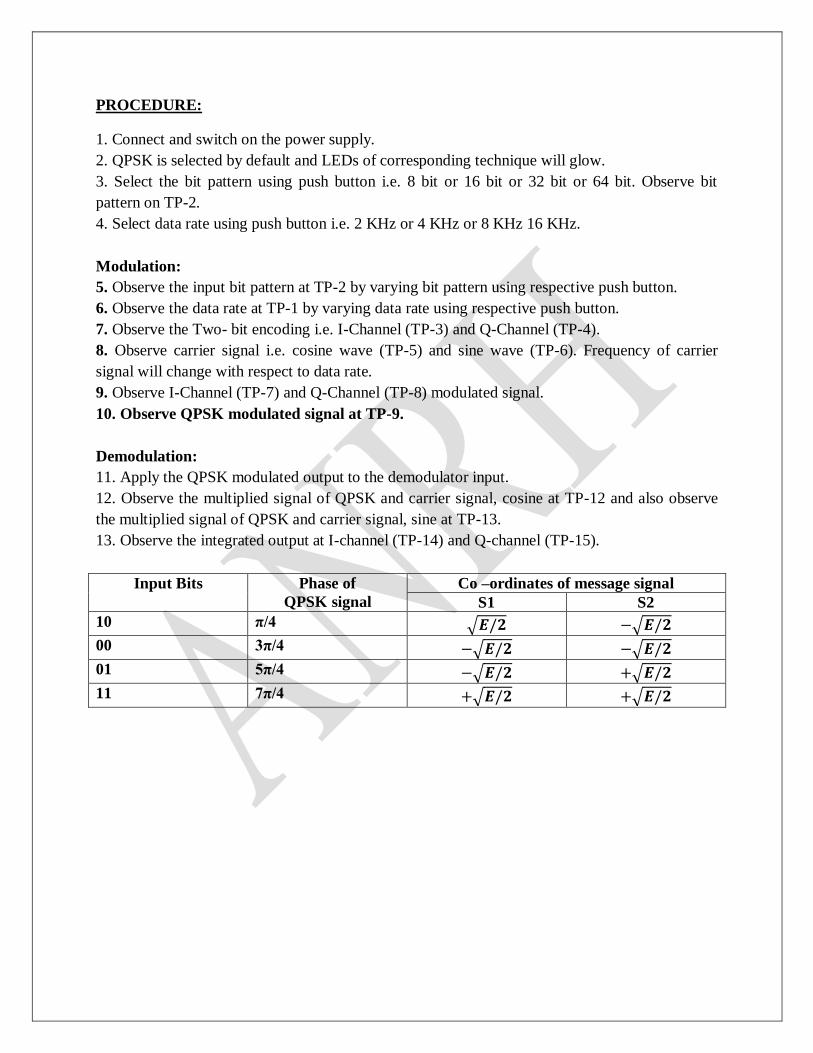
PROCEDURE:
1. Connect and switch on the power supply.
2. QPSK is selected by default and LEDs of corresponding technique will glow.
3. Select the bit pattern using push button i.e. 8 bit or 16 bit or 32 bit or 64 bit. Observe bit
pattern on TP-2.
4. Select data rate using push button i.e. 2 KHz or 4 KHz or 8 KHz 16 KHz.
Modulation:
5. Observe the input bit pattern at TP-2 by varying bit pattern using respective push button.
6. Observe the data rate at TP-1 by varying data rate using respective push button.
7. Observe the Two- bit encoding i.e. I-Channel (TP-3) and Q-Channel (TP-4).
8. Observe carrier signal i.e. cosine wave (TP-5) and sine wave (TP-6). Frequency of carrier
signal will change with respect to data rate.
9. Observe I-Channel (TP-7) and Q-Channel (TP-8) modulated signal.
10. Observe QPSK modulated signal at TP-9.
Demodulation:
11. Apply the QPSK modulated output to the demodulator input.
12. Observe the multiplied signal of QPSK and carrier signal, cosine at TP-12 and also observe
the multiplied signal of QPSK and carrier signal, sine at TP-13.
13. Observe the integrated output at I-channel (TP-14) and Q-channel (TP-15).
Input Bits Phase of
QPSK signal
Co –ordinates of message signal
S1 S2
10 π/4 √𝑬/𝟐 −√𝑬/𝟐
00 3π/4 −√𝑬/𝟐 −√𝑬/𝟐
01 5π/4 −√𝑬/𝟐 +√𝑬/𝟐
11 7π/4 +√𝑬/𝟐 +√𝑬/𝟐
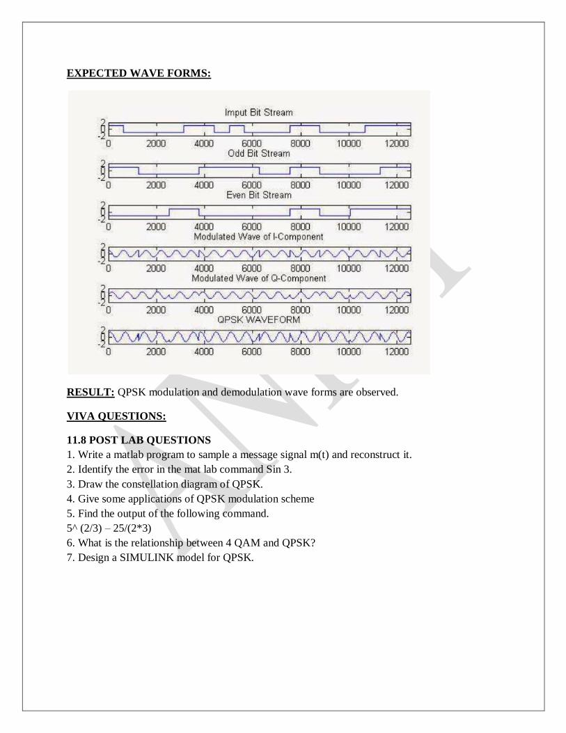
EXPECTED WAVE FORMS:
RESULT: QPSK modulation and demodulation wave forms are observed.
VIVA QUESTIONS:
11.8 POST LAB QUESTIONS
1. Write a matlab program to sample a message signal m(t) and reconstruct it.
2. Identify the error in the mat lab command Sin 3.
3. Draw the constellation diagram of QPSK.
4. Give some applications of QPSK modulation scheme
5. Find the output of the following command.
5^ (2/3) – 25/(2*3)
6. What is the relationship between 4 QAM and QPSK?
7. Design a SIMULINK model for QPSK.
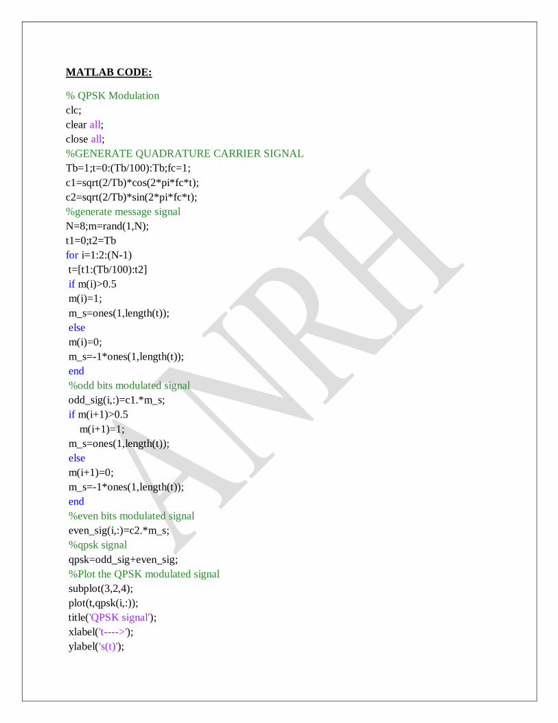
MATLAB CODE:
% QPSK Modulation
clc;
clear all;
close all;
%GENERATE QUADRATURE CARRIER SIGNAL
Tb=1;t=0:(Tb/100):Tb;fc=1;
c1=sqrt(2/Tb)*cos(2*pi*fc*t);
c2=sqrt(2/Tb)*sin(2*pi*fc*t);
%generate message signal
N=8;m=rand(1,N);
t1=0;t2=Tb
for i=1:2:(N-1)
t=[t1:(Tb/100):t2]
if m(i)>0.5
m(i)=1;
m_s=ones(1,length(t));
else
m(i)=0;
m_s=-1*ones(1,length(t));
end
%odd bits modulated signal
odd_sig(i,:)=c1.*m_s;
if m(i+1)>0.5
m(i+1)=1;
m_s=ones(1,length(t));
else
m(i+1)=0;
m_s=-1*ones(1,length(t));
end
%even bits modulated signal
even_sig(i,:)=c2.*m_s;
%qpsk signal
qpsk=odd_sig+even_sig;
%Plot the QPSK modulated signal
subplot(3,2,4);
plot(t,qpsk(i,:));
title('QPSK signal');
xlabel('t---->');
ylabel('s(t)');
grid on;
hold on;
t1=t1+(Tb+.01);
t2=t2+(Tb+.01);
end
hold off
%Plot the binary data bits and carrier signal
subplot(3,2,1);
stem(m);
title('binary data bits');
xlabel('n---->');
ylabel('b(n)');
grid on;
subplot(3,2,2);
plot(t,c1);
title('carrier signal-1');
xlabel('t---->');
ylabel('c1(t)');
grid on;
subplot(3,2,3);
plot(t,c2);
title('carrier signal-2');
xlabel('t---->');
ylabel('c2(t)');
grid on;
% QPSK Demodulation
t1=0;t2=Tb
for i=1:N-1
t=[t1:(Tb/100):t2]
%correlator
x1=sum(c1.*qpsk(i,:));
x2=sum(c2.*qpsk(i,:));
%decision device
if (x1>0&&x2>0)
demod(i)=1;
demod(i+1)=1;
elseif (x1>0&&x2<0)
demod(i)=1;
demod(i+1)=0;
elseif (x1<0&&x2<0)

demod(i)=0;
demod(i+1)=0;
elseif (x1<0&&x2>0)
demod(i)=0;
demod(i+1)=1;
end
t1=t1+(Tb+.01); t2=t2+(Tb+.01);
end
subplot(3,2,5);
stem(demod);
title('qpsk demodulated bits');
xlabel('n---->');
ylabel('b(n)');
grid on;
EXTRA
EXPERIMENTS
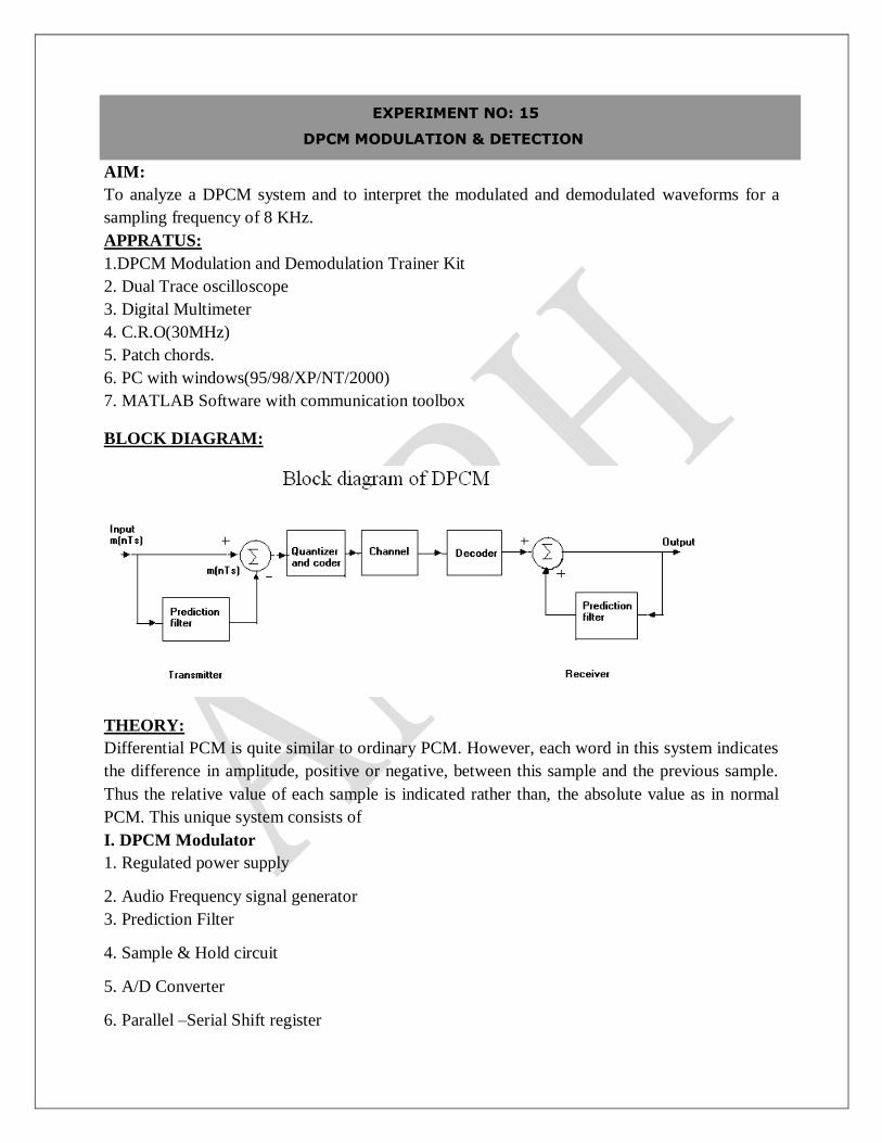
EXPERIMENT NO: 15
DPCM MODULATION & DETECTION AIM:
To analyze a DPCM system and to interpret the modulated and demodulated waveforms for a
sampling frequency of 8 KHz.
APPRATUS:
1.DPCM Modulation and Demodulation Trainer Kit
2. Dual Trace oscilloscope
3. Digital Multimeter
4. C.R.O(30MHz)
5. Patch chords.
6. PC with windows(95/98/XP/NT/2000)
7. MATLAB Software with communication toolbox
BLOCK DIAGRAM:
THEORY:
Differential PCM is quite similar to ordinary PCM. However, each word in this system indicates
the difference in amplitude, positive or negative, between this sample and the previous sample.
Thus the relative value of each sample is indicated rather than, the absolute value as in normal
PCM. This unique system consists of
I. DPCM Modulator
1. Regulated power supply
2. Audio Frequency signal generator
3. Prediction Filter
4. Sample & Hold circuit
5. A/D Converter
6. Parallel –Serial Shift register
7. Clock generator / Timing circuit
8. DC source
II. DPCM Demodulator
1. Regulated Power Supply
2. Serial-Parallel Shift registers.
3. D/A converter.
4. Clock generator
5. Timing circuit
6. Prediction filter
7. Passive low pass filter
PROCEDURE:
1. Study the theory of operation thoroughly.
2. Connect the trainer (Modulator) to the mains and switch on the power supply.
3. Observe the output of the AF generator using CRO, it should be Sine wave of 400 Hz
frequency with 3V pp amplitude.
4. Verify the output of the DC source with multi-meter/scope; output should vary 0 to +290mV.
5. Observe the output of the Clock generator using CRO, they should be 64 KHz and 8 KHz
frequency of square with 5 Vpp amplitude.
6. Connect the trainer (De Modulator) to the mains and switch on the power supply.
7. Observe the output of the Clock generator using CRO; it should be 64 KHz square wave with
amplitude of 5 pp.
DPCM Operation (with DC input):
Modulation:
8. Keep CRO in dual mode. Connect one channel to 8 KHz signal (one which is connected to the
Shift register) and another channel to the DPCM output.
9. Observe the DPCM output with respect to the 8 KHz signal and sketch the waveform.
10. Note: Form this waveform you can observe that the LSB bit enters the output first.
11. Set DC source to some value say 1 V with the help of multi-meter and connect it to the A/D
converter input and observe the output LED’s.
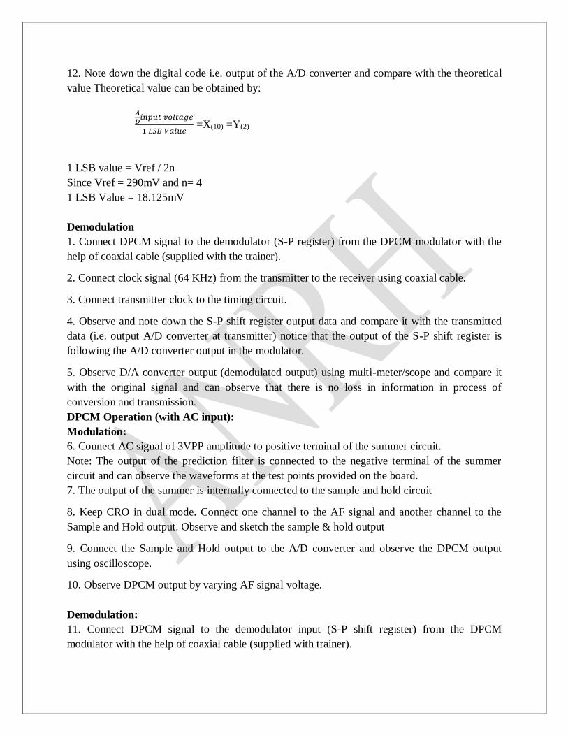
12. Note down the digital code i.e. output of the A/D converter and compare with the theoretical
value Theoretical value can be obtained by:
𝐴
𝐷𝑖𝑛𝑝𝑢𝑡 𝑣𝑜𝑙𝑡𝑎𝑔𝑒
1 𝐿𝑆𝐵 𝑉𝑎𝑙𝑢𝑒 =X(10) =Y(2)
1 LSB value = Vref / 2n
Since Vref = 290mV and n= 4
1 LSB Value = 18.125mV
Demodulation
1. Connect DPCM signal to the demodulator (S-P register) from the DPCM modulator with the
help of coaxial cable (supplied with the trainer).
2. Connect clock signal (64 KHz) from the transmitter to the receiver using coaxial cable.
3. Connect transmitter clock to the timing circuit.
4. Observe and note down the S-P shift register output data and compare it with the transmitted
data (i.e. output A/D converter at transmitter) notice that the output of the S-P shift register is
following the A/D converter output in the modulator.
5. Observe D/A converter output (demodulated output) using multi-meter/scope and compare it
with the original signal and can observe that there is no loss in information in process of
conversion and transmission.
DPCM Operation (with AC input):
Modulation:
6. Connect AC signal of 3VPP amplitude to positive terminal of the summer circuit.
Note: The output of the prediction filter is connected to the negative terminal of the summer
circuit and can observe the waveforms at the test points provided on the board.
7. The output of the summer is internally connected to the sample and hold circuit
8. Keep CRO in dual mode. Connect one channel to the AF signal and another channel to the
Sample and Hold output. Observe and sketch the sample & hold output
9. Connect the Sample and Hold output to the A/D converter and observe the DPCM output
using oscilloscope.
10. Observe DPCM output by varying AF signal voltage.
Demodulation:
11. Connect DPCM signal to the demodulator input (S-P shift register) from the DPCM
modulator with the help of coaxial cable (supplied with trainer).
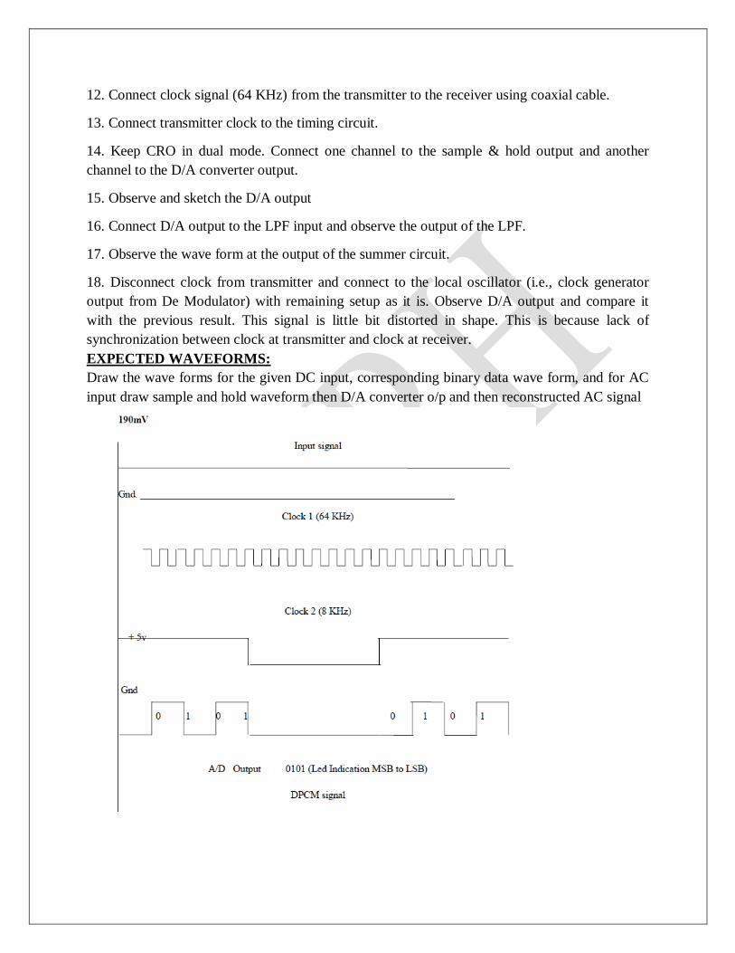
12. Connect clock signal (64 KHz) from the transmitter to the receiver using coaxial cable.
13. Connect transmitter clock to the timing circuit.
14. Keep CRO in dual mode. Connect one channel to the sample & hold output and another
channel to the D/A converter output.
15. Observe and sketch the D/A output
16. Connect D/A output to the LPF input and observe the output of the LPF.
17. Observe the wave form at the output of the summer circuit.
18. Disconnect clock from transmitter and connect to the local oscillator (i.e., clock generator
output from De Modulator) with remaining setup as it is. Observe D/A output and compare it
with the previous result. This signal is little bit distorted in shape. This is because lack of
synchronization between clock at transmitter and clock at receiver.
EXPECTED WAVEFORMS:
Draw the wave forms for the given DC input, corresponding binary data wave form, and for AC
input draw sample and hold waveform then D/A converter o/p and then reconstructed AC signal
OBSERVATIONS: DPCM with AC input
Amplitude Time period
AC Input
Prediction Filter Output
Sample and Hold Output
Clock -1 output
DPCM Output
Demodulation:
Amplitude Time period
DPCM Input
D/A Converter Output
LPF Output
Demodulation Output
Prediction Filter output
RESULT:
Thus the Differential Pulse code modulation and demodulation were performed.
VIVA QUESTIONS:
1. For data compression says whether ADPCM or DPCM is better. Justify.
2. What is the need for compression? Mention the types of compression.
3. List the communication standards which use DPCM.
4. Based upon the knowledge that you have gained after doing the experiment write the
Functions of sample and hold circuit.
5. Name the circuit used to achieve synchronization between transmitter and receiver.
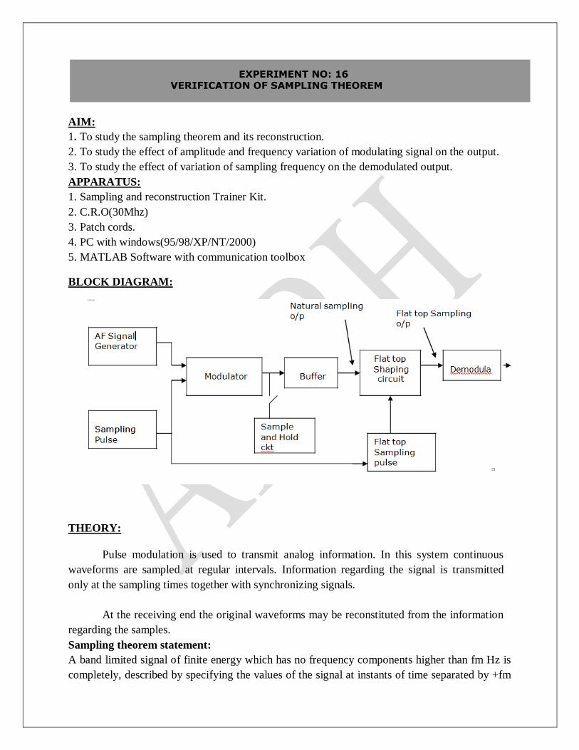
EXPERIMENT NO: 16 VERIFICATION OF SAMPLING THEOREM
AIM:
1. To study the sampling theorem and its reconstruction.
2. To study the effect of amplitude and frequency variation of modulating signal on the output.
3. To study the effect of variation of sampling frequency on the demodulated output.
APPARATUS:
1. Sampling and reconstruction Trainer Kit.
2. C.R.O(30Mhz)
3. Patch cords.
4. PC with windows(95/98/XP/NT/2000)
5. MATLAB Software with communication toolbox
BLOCK DIAGRAM:
THEORY:
Pulse modulation is used to transmit analog information. In this system continuous
waveforms are sampled at regular intervals. Information regarding the signal is transmitted
only at the sampling times together with synchronizing signals.
At the receiving end the original waveforms may be reconstituted from the information
regarding the samples.
Sampling theorem statement:
A band limited signal of finite energy which has no frequency components higher than fm Hz is
completely, described by specifying the values of the signal at instants of time separated by +fm
sec.
The sampling theorem states that if the sampling rate in any pulse modulation system
exceeds twice the maximum signal frequency, the original signal can be reconstructed in the
receiver with minimum distortion.
Fs> 2fm is called Nyquist rate Where Fs sampling frequency, Fm modulating signal frequency.
If we reduce the sampling frequency Fs less than 2fm the side bands and the information
signal will overlap and we cannot recover the information signal by low pass filter. This
phenomenon is called fold over distortion or aliasing.
There are two methods of sampling
1. Natural sampling.
2. Flat top sampling.
Sample and hold circuit holds the sampled value until the next sample is taken. Sample
and hold technique is used to maintain reasonable pulse energy. The duty cycle is defined as the
ratio of pulse duration to the pulse repetition period.
PROCEDURE:
1. Switch on the ”power ON” switch.
2. Observe the AF signal generator output, it is a sine wave frequency varying from 2
KHz to 20 KHz and amplitude varying from 0-5 Vp-p.
3. Observe the sampling pulse generator output, it is a square wave of frequency varying
from Date: 2 KHz to 32 KHz and pulse also adjustable.
4. Connect the sampling pulse generator output to the sampling pulse output of the
modulator. Make sure that the frequency adjust pot is in its extreme clock wise
direction.
5. Now adjust the output of the AF signal generator to 1 KHz, 5Vp-p and connect the
same signal to analog input terminals of the modulator. If the pulse width is now made
very narrow the SH signal will seen as if it is instantaneously sampled and held.
6. If the jumper J12 is removed-natural top sampling output is observed.
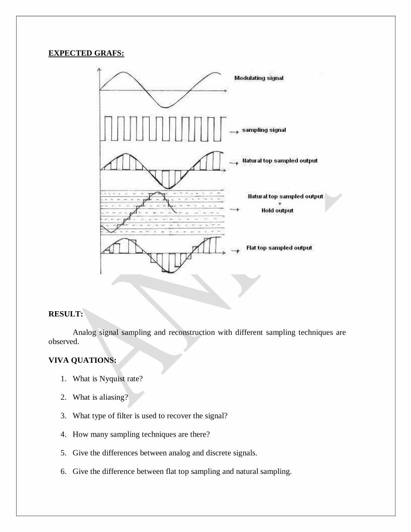
EXPECTED GRAFS:
RESULT:
Analog signal sampling and reconstruction with different sampling techniques are
observed.
VIVA QUATIONS:
1. What is Nyquist rate?
2. What is aliasing?
3. What type of filter is used to recover the signal?
4. How many sampling techniques are there?
5. Give the differences between analog and discrete signals.
6. Give the difference between flat top sampling and natural sampling.