e-newsletter deity oct 2013
DESCRIPTION
aTRANSCRIPT
GOVERNMENT OF INDIA
Department of Electronics and Information Technology (DeitY)
Ministry of Communications & Information Technology
ELECTRONICS e-NEWSLETTER
…. For Electronics System Design & Manufacturing (ESDM) Sector
Year 3 | Vol. 24: October 2013
Electronics e-Newsletter, Room No. 2280, Department of Electronics and Information Technology Ministry of Communications & Information Technology, Electronics Niketan, 6, CGO Complex, New Delhi 110003
• Semiconductor Wafer Fabs get in-principle approval • Skill development of 90,000 persons
• 12 Medical Equipments to get standards soon • FDI in excess of 26% allowed in Defence Pdn.
From Chief Editor’s Desk
Dear Readers,
A very happy Deepawali for all our readers! Wish all a happy and prosperous year ahead.
The month of October saw two major steps being taken by the Government in its push to promote the Electronics
System Design and Manufacturing. The Department of Electronics and IT (DeitY) issued in-principle approval to the two
semiconductor wafer fab projects. Moreover, it also floated an Expression of Interest for any other company which may be
interested in setting up of a similar fab with a similar package of incentives. This is indeed great as it provides an opportunity
for any other company or consortia to also seek benefit as announced by the Government.
The DeitY also approved a Rs 113.7 Crore scheme for skill development in the area of electronics. The scheme aims
to provide assistance to 90,000 students and youth in six states and works through training partners. The scheme
symbolizes the need for greater role for the Sector Skills Councils, both Telecom and Electronics, in training people in skills
needed by the industry. It also encourages private training institutions to come forward in close cooperation with the Sector
Skills Councils and National Institute of Electronics and IT (NIELIT) to provide training. Our human resource is our greatest
USP in developing this sector and the approval of the scheme is a step in that direction.
Another new initiative taken up by DeitY has been the decision to create an online platform on its website where companies
which are interested in offering technology can post their details. Similarly, companies looking for joint ventures etc can also be
posted on this platform. We expect to evolve the platform based on the user feedback and requirements as we go along.
Six Electronic Manufacturing Clusters have been given in-principle approval. The promoters need to come back with
their DPRs at the earliest so that the final approvals can be issued and the process of setting up these new centres of
electronic manufacturing takes shape. It is also essential that the State Governments take ownership of these EMCs in a big
way. A big contribution of the State Government could be providing clearances like electricity, water, building permission,
sewerage through a single point of contact for all units within the EMCs. This single decision could make a big difference in
getting investments into the State.
There seems to be slowdown in the MSIPS applications. We look forward to greater interest in the coming weeks and
months.
Dr. Ajay Kumar
For feedback and subscription, please contact: Mr. Akhilesh Saurikhia, Editor (Electronics e-Newsletter) & Consultant (Communication & Brand Building), Electronics System Design & Manufacturing (PMU), Department of Electronics and Information Technology, Ministry of Communications & Information
Technology, Electronics Niketan, 6 CGO Complex, New Delhi 110003, P: +91 1124301281, F: +91-1124364185, M: +91 9899543533, E: [email protected]
ELECTRONICS e-NEWSLETTER …. For Electronics System Design & Manufacturing (ESDM)
• Semiconductor Wafer Fabs get in-principle approval
| Page 2
Semiconductor Wafer Fabs get in-principle approval
The Cabinet on September 12, 2013 gave in-principle approval for setting up of two Semiconductor Wafer
Fabrication (FAB) Manufacturing Facilities in the country along with the incentives proposed for the two FABs. Following this,
Government has issued letters of “in principle” approval to the two bidders.
The Cabinet also advised that all other semiconductor wafer fabrication manufacturers may also be appropriately
and fully apprised of the quantum of subsidy/other benefits/support being offered for establishing FAB facilities in India.
Such manufacturers may be asked to indicate their interest/ send their responses on specified parameters to the
Department of Electronics and Information Technology within a period of four weeks and the matter along with the analysis
of the responses received is to be brought for consideration of the Cabinet.
Accordingly, Government of India has invited companies from all over the globe to Setup Fabs in India. The technical
requirements, the structure of incentives, the requirement of equity structure and other terms are indicated in the format
for Expression of Interest (EoI) issued on Oct 9, 2013 and available on the website of the Department of Electronics and
Information Technology (www.deity.gov.in). Entities fulfilling the requirements may respond in the prescribed format, within
a period of four weeks, from the date of issue.
Companies already operating/ running a semiconductor wafer fabrication/ manufacturing unit either as an owner of
the technology or in case it is manufacturing under license, companies may apply either on their own or as a consortium.
Template for submitting an expression of Interest is given in the EoI document. Incentives or Support to be made available by
Govt. of India are as under:
i. The incentives under Modified Special Incentive Package Scheme (M-SIPS) Policy notified by the Government of India
on 27th July 2012 may be provided to the extent of 25% of the capital expenditure of the project.
ii. A 25% subsidy on growth capital expenditure as admissible under M-SIPS Policy may be provided.
iii. Countervailing Duty (CVD) on purchase of capital goods may be reimbursed as admissible under M-SIPS Policy.
iv. Excise duty paid on the products of the Fab may be reimbursed under the existing M-SIPS Policy, for a period of 10 years.
v. The duties and levies in the form of Basic Customs Duty (BCD), as applicable may be exempted not only for all the
items covered under ITA-1 (of WTO) but also for all other capital goods required for the project including items of civil
(except basic materials like cement and steel), electrical and including growth capital as also consumables and raw
material required for the production from Fab.
vi. 200% deduction may be allowed for the expenditure on R&D as admissible under Section 35(2AB) of the Income-Tax Act.
vii. Expenditure to be incurred for the training of the project personnel may be reimbursed in terms of National Skills
Development Corporation (NSDC) Scheme.
viii. Investment linked deduction under Section 35AD of the Income-tax Act may be considered.
ix. Disbursement of MSIPS reimbursement may be made pari passu on a quarterly basis as against the annual basis as
envisaged in the M-SIPS Policy.
x. Viability Gap Funding (VGF) may be provided in the form of an interest-free loan with following terms:-
a. On commencement of commercial operations part of the VGF would be converted into 11% equity at face value.
The balance of the VGF shall have a moratorium of 10 years from commissioning of respective phases or the year
of break even, whichever is earlier, and repayable in 5 equal annual installments thereafter.
b. VGF may be provided up to ceiling amount of 20% of the CAPEX, including the Growth CAPEX of the project, or
INR 5,200 Crores (INR 52 Billion) (in nominal value), whichever is less. The exact quantum of VGF will be decided
by the GOI after the appraisal of the DPR submitted by the applicant consortium, duly taking into account the
benefits available under Section 35AD of the Income Tax Act (as per sub-para (viii) above).
c. VGF which shall be provided as an interest free loan and shall be disbursed, on a pari passu basis with CAPEX by the SPV.
d. VGF shall be used for replacing of project debt and shall not be used for reducing the promoters’ equity.
….. contd. on page 3.

• Skill development of 90,000 persons • Kinfra’s Applications for setting up Greenfield EMC
….. contd. from page 2
Further, in consideration of the support provided by the Government, the promoters shall offer a golden share to
the Government of India (GOI) or to the CPSU(s) to be nominated by the Government of India. Government of India shall
have the right to nominate one Director on the Board of the SPV. The nominee Director of the GOI shall have the power to
block any special resolution of the Board, in the public interest but this shall not apply to normal commercial decisions for
running the fab. An appropriate Shareholders Agreement shall be put in place to give effect to the foregoing requirements.
If applicant is applying as a consortium, the equity participation of the principal technology partner should be at least
10% in the SPV. The capital structure of the SPV shall not be changed without the approval of the Government of India.
Expression of Interest document released on Oct 09, 2013 is available on www.deity.gov.in. For more details, please
contact, Shri S.K. Marwaha, Scientist ‘F’, DeitY (email: [email protected]).
| Page 3
ELECTRONICS
e-NEWSLETTER …. For Electronics System Design & Manufacturing (ESDM)
Electronics e-Newsletter, Room No. 2280, Department of Electronics and Information Technology Ministry of Communications & Information Technology, Electronics Niketan, 6, CGO Complex, New Delhi 110003
Rs 113.7 Crores scheme for Skill development of 90,000 persons in Electronics sector
The Department of Electronics and IT (DeitY) has approved a scheme to support skill development in electronics and
related areas. The scheme will be implemented in six states/UTs. These states and UTs will now be identified by the DeitY.
Under the scheme, 75% of the course fee is provided as assistance. Various vocational courses ranging from 200
hours to 400 hours will be eligible for assistance. In addition, full registration and certification fee would be reimbursed.
Assistance is also provided for the implementing agency.
The scope of the scheme is not limited by pre-decided courses. The courses supported will be based on industry
requirement. The students may undergo training either full-time or part-time. Students having passed IX/ X standards
onwards, ITI and Polytechnic programmes, Under Graduate (Non-Engineering) as well as Unemployed youth like School
dropouts from 8th Pass onwards, ITI Certificate Holders, Diploma holders, Graduates(non-engineering), Registrants in
Employment Exchanges and Unemployed resources in the Non-formal Sector, etc., will be covered under this scheme.
The training shall be provided by either NIELIT or NIELIT accredited centres or other training partners recognized by
the Electronic Sector Skills Council and the Telecom Sector Skills Council. The courses would be those accredited by NIELIT or
the aforesaid two Sector Skills Councils.
The scheme will be implemented in a decentralized manner. Each State/UT shall identify an implementing agency to
interact with training partners within their States to implement the scheme.
An empowered Committee headed by the Secretary, DeitY has been constituted for implementing the scheme. The
Empowered committee will include representatives of Planning Commission, DG, NSDA, CEOs of NSDC, ESSC, TSSC.
For more information, please contact Shri A.K. Arora, Director, Deity (Email: [email protected]) or Shri Sanjay
Vyas, Joint Director, DeitY (Email: [email protected]).
Kinfra’s Applications for setting up Greenfield EMC at Kakhanad
Further to applications for setting-up Greenfield and Brownfield Electronic Manufacturing Clusters reported in
previous editions of the Electronics e-Newsletter, an application from Kerala Industrial Infrastructure Development
Corporation (KINFRA) has been received for developing an Electronics Manufacturing Cluster at Kakhanad in an area of 75
acres at an estimated project cost of Rs. 250 Crores.
Details regarding approved EMCs the contact details of concerned persons regarding EMCs are also available on
website www.deity.gov.in/esdm. For more information, please contact Nodal Officer, EMC Scheme. Shri Rajneesh Agrawal,
Director DeitY (Email: [email protected]) or Shri Sanjay Koul, AD, DeitY (Email: [email protected]).
• 12 Medical Equipments to get Standards • Status of Workload of Labs under CRS
| Page 4
ELECTRONICS e-NEWSLETTER …. For Electronics System Design & Manufacturing (ESDM)
Electronics e-Newsletter, Room No. 2280, Department of Electronics and Information Technology Ministry of Communications & Information Technology, Electronics Niketan, 6, CGO Complex, New Delhi 110003
12 Medical Equipments to get Standards soon
A meeting was held between Shri Kapil Sibal, Hon’ble Minister for Communications and IT and for Law and Justice
and Prof. K.V. Thomas, Hon’ble MoS for Consumer Affairs, Food and Public Distribution on Sept 19, 2013 to review the
progress regarding finalization of standards in respect of 12 medical equipments. It was arrived at that the target date/
timeline committed by Bureau of Indian Standards for finalizing the standards in respect of 12 equipments will be strictly
adhered to. Medical Equipments for which standards are being finalized are:
• Capsule endoscope • Pulse Oximeter
• Behind the ear digital programmable Hearing Aid • Electronic Stethoscope
• Neuro Stimulator • Biochemistry Analyser
• Sacral & Gastric neuromodulation system • ECG Machine
• Permanent Pacemaker • Lungs ventilator
• Diabetic care devices • Mammography for breast cancer
The matter regarding progress of grant of registration under the self-declaration scheme for electronic items was
also discussed. It was decided that all the incomplete applications for grant of registration will be taken up on priority. If
necessary, a special cell will be created to dispose this by inviting applications and sort out the matters in one go.
Hon’ble MCIT expressed that BIS should grant registration on fast track basis and the supply chain should not
stop. Hon’ble MCIT asked BIS to reconsider the matter regarding BIS requirement concerning the font size for labelling
on the registered goods.
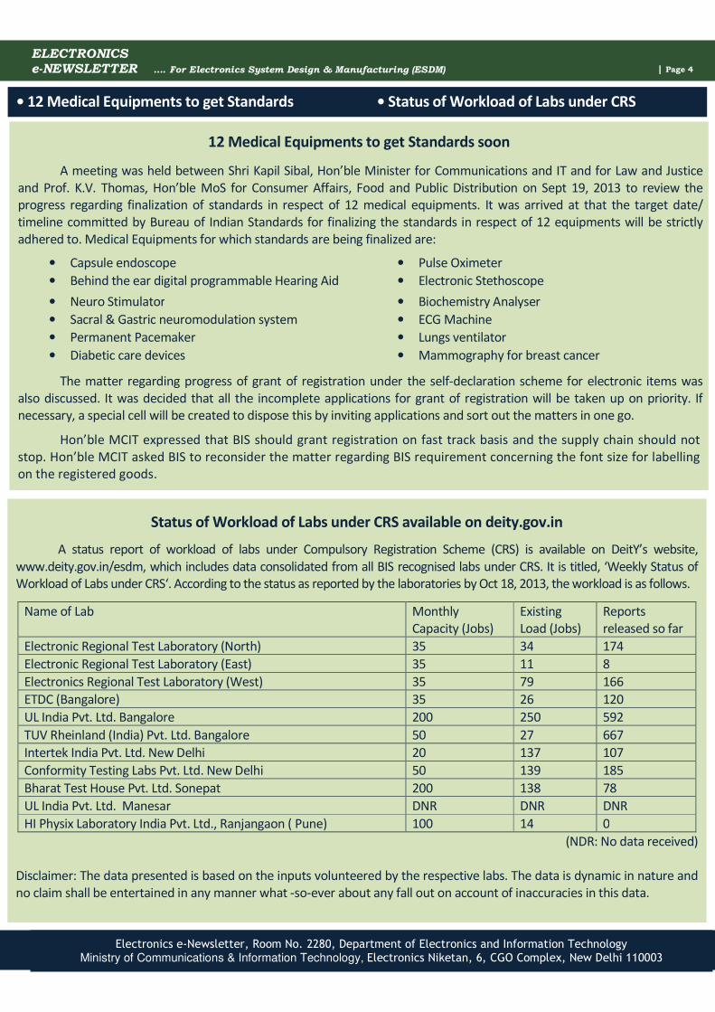
Status of Workload of Labs under CRS available on deity.gov.in
A status report of workload of labs under Compulsory Registration Scheme (CRS) is available on DeitY’s website,
www.deity.gov.in/esdm, which includes data consolidated from all BIS recognised labs under CRS. It is titled, ‘Weekly Status of
Workload of Labs under CRS‘. According to the status as reported by the laboratories by Oct 18, 2013, the workload is as follows.
Name of Lab Monthly
Capacity (Jobs)
Existing
Load (Jobs)
Reports
released so far
Electronic Regional Test Laboratory (North) 35 34 174
Electronic Regional Test Laboratory (East) 35 11 8
Electronics Regional Test Laboratory (West) 35 79 166
ETDC (Bangalore) 35 26 120
UL India Pvt. Ltd. Bangalore 200 250 592
TUV Rheinland (India) Pvt. Ltd. Bangalore 50 27 667
Intertek India Pvt. Ltd. New Delhi 20 137 107
Conformity Testing Labs Pvt. Ltd. New Delhi 50 139 185
Bharat Test House Pvt. Ltd. Sonepat 200 138 78
UL India Pvt. Ltd. Manesar DNR DNR DNR
HI Physix Laboratory India Pvt. Ltd., Ranjangaon ( Pune) 100 14 0
(NDR: No data received)
Disclaimer: The data presented is based on the inputs volunteered by the respective labs. The data is dynamic in nature and
no claim shall be entertained in any manner what -so-ever about any fall out on account of inaccuracies in this data.
• Draft Policy on Mega ESDM Projects
Disclaimer: For full details on any particular issue, readers may refer to official published documents and policies on the subject. Though every care has been taken to ensure correctness of content, DeitY or its employees are not directly/ indirectly responsible for any inaccuracy in facts, figures or their interpretation.
Discrepancy if any may be brought to the notice of Editor. For Copyright, Hyperlinking and Privacy Policy, please refer to DeitY’s website, www. deity.gov.in
| Page 5
ELECTRONICS e-NEWSLETTER …. For Electronics System Design & Manufacturing (ESDM)
Draft Policy on Mega Electronics System Design and Manufacturing (ESDM) Projects
National Policy on Electronics (NPE), 2012 lays down an ambitious vision of enhancing the current level of
manufacture in the ESDM sector, from USD 70 Billion to USD 400 Billion, to meet the domestic demand for electronic
products. To achieve this objective of attracting large electronics manufacturing companies to invest in India, the DeitY is has
floated a ‘Mega Projects Policy for Electronics’. The policy is aimed to attract large investments in the sector.
According to the draft, a Mega Project is defined as a proposal for establishing one or more large clusters of facilities
in the ESDM sector for undertaking any or all of the activities of ESDM, at one or more locations in India, including design,
development, manufacturing, packaging, marking and testing, for domestic sale or for exports. The size of capital
investment committed should be over USD 1 Billion, spread over the 5 years (i.e. FY 2013-14 to 2117-18), supported by a
clear roadmap for the proposed lines of activities/ products and the corresponding streams of investment. For this purpose,
the 'eligible investment' shall include:
o Investments in establishing the India manufacturing supply-chain
o Made by the manufacturing partners and EMS partners in establishing manufacturing facilities in India
o In R&D facilities and
o In development of supplier and component manufacturing eco- system for ESDM
A credible marketing plan need to accompany the proposal to support a proposed annual turnover of USD 4 Billion
to be reached by 31-3-2020, with an intermediate milestone of USD 2 Billion to be reached by 31-3- 2017. The manufacture
and marketing plan for the Mega Project should also specify the manner in which the same would be aligned to meet the
strategic objectives of the NPE, 2012. A commitment is made by the promoters to generate employment in line with the
industry norms applicable to the proposed verticals. The promoters of the Mega Project shall also endeavour to achieve the
following objectives while implementing the project:
i. Leverage their global OEM technology, standards, and their experience in building an ESDM eco-system or sub-
system for supporting the initiatives of GOI for promotion of manufacturing activities in India.
ii. Work towards developing India as a strategic node and a global sourcing hub in their manufacturing network,
including meeting global demand through exports out of India, adopting the "Manufacture for the Globe" approach.
iii. Undertake/ enhance their research and development activities in India, with a special focus on the products manufactured
through the Mega Project and on products to be specially designed for the markets in India and the region.
iv. Contribute towards development of an eco-system supportive of high-end manufacturing on a sustainable basis,
including the development of back-end supply chain and skill base for the ESDM sector.
The following additional incentives are proposed for eligible Mega Projects:
i. Applying PMA across a portfolio of products: In respect of domestic manufacturers, who establish a Mega Project,
producing multiple (more than one) products in India, the value addition will be calculated and applied across the
entire portfolio of products produced in India. The following conditions apply:
a. Only the products that have contributed at least 15 of the total sales across the ESDM portfolio (in India) during
the previous financial year would be eligible to be considered for applicability of liberalized value addition norms
under this provision.
b. The value addition norm may be calculated for the entire portfolio of products produced in India, with weightages for
each product in proportion to the production achieved for each product during the previous FY, in value terms.
ii. Deemed Domestic Manufacture (DDM): In respect of domestic manufacturers, who establish a Mega Project one or
more of their products shall be deemed to have been manufactured domestically, even when produced abroad. The
following conditions apply:
a. The domestic manufacturer, establishing a Mega Project, shall be given a credit of DDM, computed as a
percentage of the value of products manufactured in India, that satisfy the prescribed value addition norms.
…. Contd. on page 6
• Draft Policy on Mega ESDM Projects ……… • IITB’s programmes on ‘Semiconductor Technology
| Page 6
ELECTRONICS e-NEWSLETTER …. For Electronics System Design & Manufacturing (ESDM)
Electronics e-Newsletter, Room No. 2280, Department of Electronics and Information Technology Ministry of Communications & Information Technology, Electronics Niketan, 6, CGO Complex, New Delhi 110003
…. Contd. from page 5
b. Such manufacturer will be allowed to import products of a value not exceeding such a DDM credit limit and such
imported products shall be deemed to have been manufactured in India for the purpose of PMA.
c. The percentage of the value of products manufactured in India, which shall be used to determine the credit limit
of DDM, shall be fixed considering the share of the products imported products (deemed to be manufactured in
India), in the total sales of the entire portfolio of products in India, during the previous financial year, including
sales to private sector.
iii. Tax Incentives: The Mega Projects shall be eligible to get the following fiscal and tax incentives, subject to fulfillment
of the other criteria as may be prescribed under the relevant fiscal and tax regulations:
a. On a request made by the promoter of the Mega Project, the GOI would endeavour to enter into a bilateral or
multilateral Advance Pricing Agreement (APA) to assure certainty in transfer pricings.
b. GOI shall take steps to notify a concessional rate on income tax on the payments made by the Mega Project to its
foreign affiliates for royalties, technical services and interest.
c. GOI shall take steps to provide exemption from the levy of dividend distribution tax on the profits distributed by
the Mega Project to its overseas parent.
d. GOI shall provide the benefits of Focus Product Scheme for the export of the products from DTA manufactured
by the Mega Project, including the goods eligible to be treated as deemed exports.
Additionally, the GOI shall provide the following covenants to facilitate the establishment of the Mega Project:
a. GOI shall establish a Single Window for enabling the promoters of the Mega Projects to obtain speedy clearances
and the concessions prescribed in this policy.
b. GOI shall assist the promoters of Mega Projects to pursue the respective state government (s) to secure
additional incentives as can be provided by those Governments.
c. The additional incentives prescribed under this policy shall be over and above those available under the normal
existing policies of the GOI.
d. The location of the Mega Project shall be treated as Brownfield Electronic Manufacturing Cluster for the purpose
of providing the incentives under NPE 2012.
The draft has been circulated to industry players and associations for their comments. A meeting was also held
under the Chairmanship of Shri J Satyanarayana, Secretary, DeitY to discuss the draft on Sept 12, 2013.
After taking into account the feedback received, the DeitY proposes to finalize the Mega Projects policy and move
for approval of the Government.
For more details, please contact, Shri S. K. Marwaha, Director, DeitY (email: [email protected]).
Second edition of ‘Semiconductor Technology and Manufacturing course’ at IITB to start in Dec. 2013 IITB conducted a Continuing Education Programme in Nov 2012 on ‘Semiconductor Technology and Manufacturing’ and
enrolled 50 delegates, 14 from industry and 36 from academia. This course run in collaboration with Applied Materials gives an
overview of the Semiconductor manufacturing process with actual hands on training on production tools used.
Based on strong positive feedback, second batch of the programme is being launched to be conducted from 10th-15th of
Dec 2013 at IIT Bombay. This is an evolved version and comes in the wake of the Government approval for Semiconductor Chip
manufacturing in the country. The 6-day course will include lectures from IIT Bombay faculty and experts from Applied Materials
on topics such as cleanrooms, tools and hardware, as well as process technology. There will be hands-on lab sessions on 200 mm
production-level tools for the course participants. Course information is available on http://www.cen.iitb.ac.in/cen/
events/cep_course.php. For more details, please contact Prof. Saurabh Lodha or Prof. Udayan Ganguly at [email protected].
• Electronic Manufacturing Cluster, Khushkera, Bhiwadi Rajasthan: An Outline
| Page 7
ELECTRONICS e-NEWSLETTER …. For Electronics System Design & Manufacturing (ESDM)
Electronics e-Newsletter, Room No. 2280, Department of Electronics and Information Technology Ministry of Communications & Information Technology, Electronics Niketan, 6, CGO Complex, New Delhi 110003
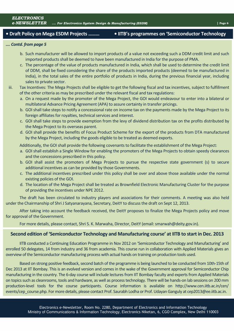
Electronic Manufacturing Cluster, Khushkera, Bhiwadi Rajasthan
M/s ELCINA Electronics Manufacturing Cluster Private Limited (EEMCPL) has proposed setting up an Electronic
Manufacturing Cluster (EMC) in Bhiwadi, Rajasthan in an area of 100.7 acres of land and has been accorded in-principle
approval by DeitY. Details of this Greenfield EMC are as under:
Environmental clearance: The applicant will be submitting Technical Environmental Impact Assessment (EIA) report about
the proposed cluster in accordance to the Guidance manual for Industrial Estates along with the final DPR.
Proposed Project for which assistance sought: EEMCPL the SPV of the project, plans to establish and develop Basic
Infrastructure Network, Utility Plants, Common Facilities, Social Welfare Facilities, etc., over an area of 527.08 acres at an
estimated project cost of Rs 100.48 Crores.
Anchor clients/Interested parties: The Cluster would also endeavour to bring the entire gamut of electronic manufacturing
operations under one umbrella and facilitate all stages of the value chain of electronic manufacturing. 19 members of the
SPV have already been identified, who have contributed Rs. 9.09 Crore.
About the promoter: The Project is proposed by ELCINA (Electronic Industries Association of India), an Association
of electronic component manufacturers; incorporated under the Companies Act 1956 in Delhi. The promoters have
incorporated a Special Purpose Vehicle in the name of “ELCINA” Electronics Manufacturing Cluster Private Limited”
(EEMC) on Nov 21, 2012, a company incorporated under the Companies Act, 1956 (“SPV”) for the purpose of
establishing the Project.
Details of In-principle Approval: The in- principle approval for setting up a Greenfield EMC at Bhiwadi, in Rajasthan has been
accorded to M/s EEMCPL on September 17, 2013 for development of common/ basic infrastructure facilities at an estimated
cost of Rs 100.48 Crores.
Contact Details: Shri. Rajoo Goel, Secretary General, ELCINA , ELCINA Electronic Industries Association of India, ELCINA
House, 422, Okhla Industrial Estate Phase III, New Delhi 110020; Phone : 91-11-41615985, 26924597,26928053; Email:
Industrial Area, Bhiwadi, Rajasthan
Proposed Site for the EMC Indl. Area
at
Khushkhera
Indl. Area -Tapukara
7 K
M f
rom
D
ha
ruh
era
Jaip
ur
–20
0 K
m
2
EMC, Bhiwadi Location Map
Location: The proposed electronic cluster is situated in IA
Salarpur, (Khushkera Extn.), Bhiwadi, Alwar District in a 100.7
acre plot of land. The Industrial Area is situated on NH 8.
Road Connectivity: Located on National Highway 8 between Its
distances from Major cities are about 40 Km from Gurgaon, 90
Km from Alwar, 175 km from Jaipur and 60 Kms from Delhi.
Airport Connectivity: Nearest Airport is IGI New Delhi at 25 Kms.
Power Availability: 2 Feeder power lines are passing from the
close proximity of the Cluster site besides two sub- station of
220KV and 132 KV are also near the cluster site. ELCINA is
contemplating setting up a captive power plant with power
backup of 30% of estimated power demand in the proposed
electronic cluster
Water Availability: The total water demand is estimated at 2.3
MLD. The water supply to the Electronic Cluster will be through
a Ground Level Service Reservoir, Pumping Station, Elevated
Level Service Reservoir (ELSR) and a Distribution System.
• Electronic Manufacturing Cluster, Bhopal, MP: An Outline
| Page 8
ELECTRONICS e-NEWSLETTER …. For Electronics System Design & Manufacturing (ESDM)
Electronics e-Newsletter, Room No. 2280, Department of Electronics and Information Technology Ministry of Communications & Information Technology, Electronics Niketan, 6, CGO Complex, New Delhi 110003
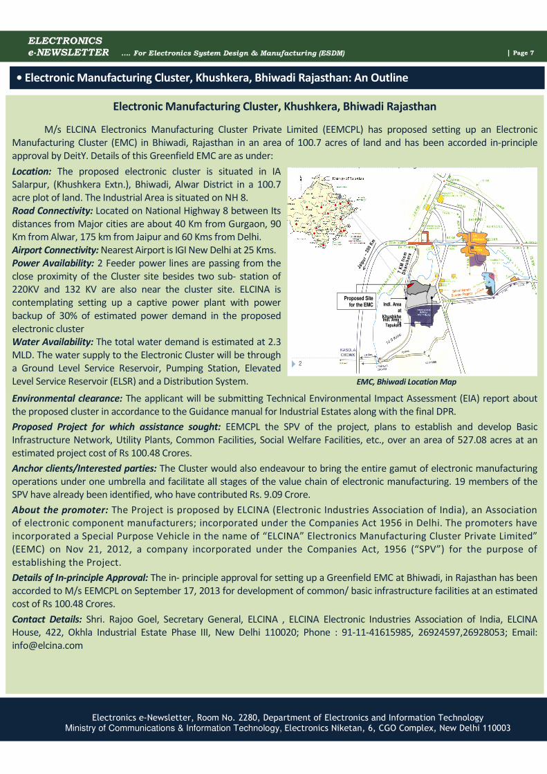
Electronic Manufacturing Cluster, Bhopal, MP
M/s Madhya Pradesh State Electronics Development Corporation Ltd. (MPSEDC) has proposed setting up an
Electronic Manufacturing Cluster (EMC) in Badwai, District Bhopal, Madhya Pradesh in an area of 50.0 acres of land and has
been accorded in-principle approval by DeitY. Details of this Greenfield EMC are as under:
Air Connectivity: Distance of the site from Bhopal International Airport is 3 km.
Inland Container Depot (ICD): The nearest ICD is situated at Mandideep, Distt. Raisen at a distance of 40 km.
Power Availability: Power to the EMC will be supplied by M.P. Power Distribution Company Ltd. of M.P. Power Transmission
Company Ltd., via a 33/11 kV substation planned within the cluster. The estimated power demand, as per the Applicant, is 7
MVA. For power backup, Diesel Generator (DG) sets would be used.
Water Availability: All water requirements (for Industries, for domestic use, for Green area maintenance, etc.) is planned to be
completed from Municipal Narmada line. Alternate provision for additional source of water will also be created through TubeWell.
Environmental clearance: The applicant will be submitting Technical Environmental Impact Assessment (EIA) report about
the proposed cluster in accordance to the Guidance manual for Industrial Estates along with the final DPR.
Proposed Project for which assistance sought: MPSEDC the chief promoter of the project plans to establish and develop
Basic Infrastructure Network, Utility Plants, Common Facilities, Social Welfare Facilities, etc. over an area of 50.0 acres at an
estimated project cost of Rs 44.25 Crores.
Anchor clients/Interested parties: MPSEDC expects to house around 30 units in the cluster (31 plots in the EMC) with
expected investments by the units in the EMC to be Rs. 260 Crore. The Applicant has received Letters of Intent from 3
prospective constituent units, M/s HLBS Tech Pvt. Ltd., M/s EVDAT Software Technology Pvt. Ltd. and M/s Bharat Business
Channel Ltd., expressing their interest to setup units in the IT Park being developed in Badwai.
About the promoter: MPSEDC is a company limited by shares and a Govt. of M.P. Undertaking headquartered at Bhopal, M.P.
and incorporated on 18th Nov 1983 at Gwalior, M.P. MPSEDC is operational under Department of Information Technology,
Govt. of M.P. as the nodal agency to promote IT in the State its scope of work includes promotion & implementation of IT and e-
Governance. MPSEDC mandate includes opportunities for software development, supply of hardware and peripherals,
networking and connectivity, web applications, ecommerce, IT Capacity building and other direct and indirect IT businesses.
Details of In-principle Approval: The in- principle approval for setting up a Greenfield EMC at Badwai, Bhopali, in Madhya
pradesh has been accorded to M/s MPSEDC on 17th September 2013 for development of common/ basic infrastructure
facilities at an estimated cost of Rs 44.25 Crores.
Contact Details: Shri L.K.Tiwari, Addl General Manager, 47-A, State-IT Centre Area Hills, Bhopal-462011; E-Mail:
[email protected], [email protected].
EMC, Badwai, Bhopal Location Map
Location: The identified site is located adjacent to Ayodhya / Old
bypass road (NH-12) between Bhopal International Airport and
Bhopal Memorial Hospital & Research Centre (BMHRC). The site of
the proposed EMC (50 acres) is part of the Information Technology
Park (212.63 acres) being developed by MPSEDC. Near to the site is
Rajiv Gandhi Technical University, Bhopal; Development
Corporation’s Aero City and Bhopal International Airport.
Road Connectivity: NH-12 (connecting Bhopal—Jabalpur) is
adjacent to the site. Bhopal Inter-State Bus Terminal (ISBT) is
situated at a distance of 20 km.
Rail Connectivity: Bhopal being in the central zone of Indian
Railways, all major trains pass through the city including
Rajdhani / Shatabdi Express. Distance of the site from the main
railway station, Bhopal is 12 km.
• Electronic Manufacturing Cluster, Purva Village Jabalpur MP: An Outline
| Page 9
ELECTRONICS e-NEWSLETTER …. For Electronics System Design & Manufacturing (ESDM)
Electronics e-Newsletter, Room No. 2280, Department of Electronics and Information Technology Ministry of Communications & Information Technology, Electronics Niketan, 6, CGO Complex, New Delhi 110003
Electronic Manufacturing Cluster, Purva Village Jabalpur MP
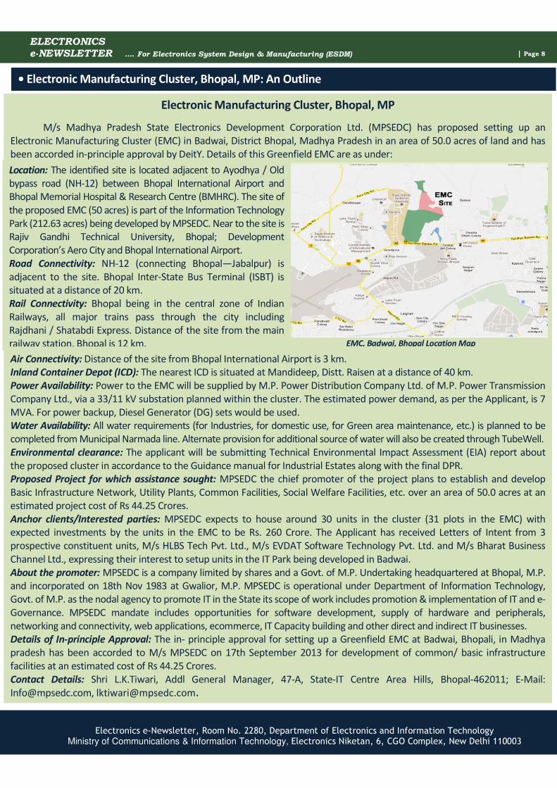
M/s Madhya Pradesh State Electronics Development Corporation Ltd. (MPSEDC) has also proposed setting up an
Electronic Manufacturing Cluster (EMC) in Purva Village, District Jabalpur, Madhya Pradesh in an area of 40.0 acres of land
and has been accorded in-principle approval by DeitY. Details of this Greenfield EMC are as under:
Power Availability: Power would be supplied by M.P. Power Distribution Company Ltd. of M.P. Power Transmission
Company Ltd., via a 33/11 kV substation planned within the cluster. The estimated power demand, as per the Applicant, is 7
MVA. For power backup, Diesel Generator (DG) sets would be used.
Water Availability: All water requirements (for Industries, for domestic use, for Green area maintenance, etc.) will be completed
from Municipal Narmada line. Alternate provision for additional source of water will also be created through TubeWell.
Environmental clearance: The applicant will be submitting Technical Environmental Impact Assessment (EIA) report about
the proposed cluster in accordance to the Guidance manual for Industrial Estates along with the final DPR.
Proposed Project for which assistance sought: MPSEDC the chief promoter of the project plans to establish and develop
Basic Infrastructure Network, Utility Plants, Common Facilities, Social Welfare Facilities, etc., over an area of 40.00 acres at an
estimated project cost of Rs 40.95 Crores.
Anchor clients/Interested parties: MPSEDC plans 39 plots (over an area of 22.03 acres) in the cluster for the manufacturing units
with expected investments by the units of Rs. 103 Crore. MPSEDC plans to target units with a specific focus on Set top box &
accessories, Solar modules, LED lighting, CCTV cameras, Medical Electronics, Control panels, Mobile charger, USB, etc.
About the promoter: MPSEDC is a company limited by shares and a Govt. of M.P. Undertaking headquartered at Bhopal, M.P.
and incorporated on Nov 18, 1983 at Gwalior, M.P. MPSEDC is operational under Department of Information Technology, Govt.
of M.P. as the nodal agency to promote IT in the State its scope of work includes promotion & implementation of IT and e-
Governance. MPSEDC mandate includes opportunities for software development, supply of hardware and peripherals,
networking and connectivity, web applications, ecommerce, IT Capacity building and other direct and indirect IT businesses.
Details of In-principle Approval: The in- principle approval for setting up a Greenfield EMC at Badwai, Bhopali, in Madhya
pradesh has been accorded to M/s MPSEDC on Sept. 17, 2013 for development of common/ basic infrastructure facilities at
an estimated cost of Rs 40.95 Crores.
Contact Details: Shri L.K.Tiwari, Addl General Manager, 47-A, State-IT Centre Area Hills, Bhopal-462011, e-Mail:
[email protected], [email protected].
EMC, Purva, Jabalpur Location Map
Location: The identified site for the proposed EMC (40 acres) is
part of the IT Park (61.8 acres) being developed by MPSEDC. The
site is located on a hillock in Bargi Hills (Nagpur Road) area in
southwest part of Jabalpur city. The surrounding region has
good amount of residential areas, hospitals, schools and
colleges in the vicinity including ‘Naya Gaon’ residential colony,
Gyan Ganga College of Technology and Netaji Subhash Chandra
Bose Medical college. The site is located within the boundary of
Jabalpur Municipal Corporation.
Road Connectivity: NH-7 (connecting Bangalore-Kanyakumari)
is adjacent to the site and is 8 kms from the main bus-stand.
Rail Connectivity: Distance of the site from the main railway
station is 11 km.
Air Connectivity: Distance of the site from the Airport is 24 km.
Inland Container Depot (ICD): The nearest ICD is situated at
Nagpur (Maharashtra) at a distance 270 km and at Mandideep,
Distt. Raisen (M.P.) at a distance of 280 km.
• IECEE discusses Compulsory Registration Scheme with DeitY
| Page 10
ELECTRONICS e-NEWSLETTER …. For Electronics System Design & Manufacturing (ESDM)
Electronics e-Newsletter, Room No. 2280, Department of Electronics and Information Technology Ministry of Communications & Information Technology, Electronics Niketan, 6, CGO Complex, New Delhi 110003
IECEE discusses Compulsory Registration Scheme with DeitY
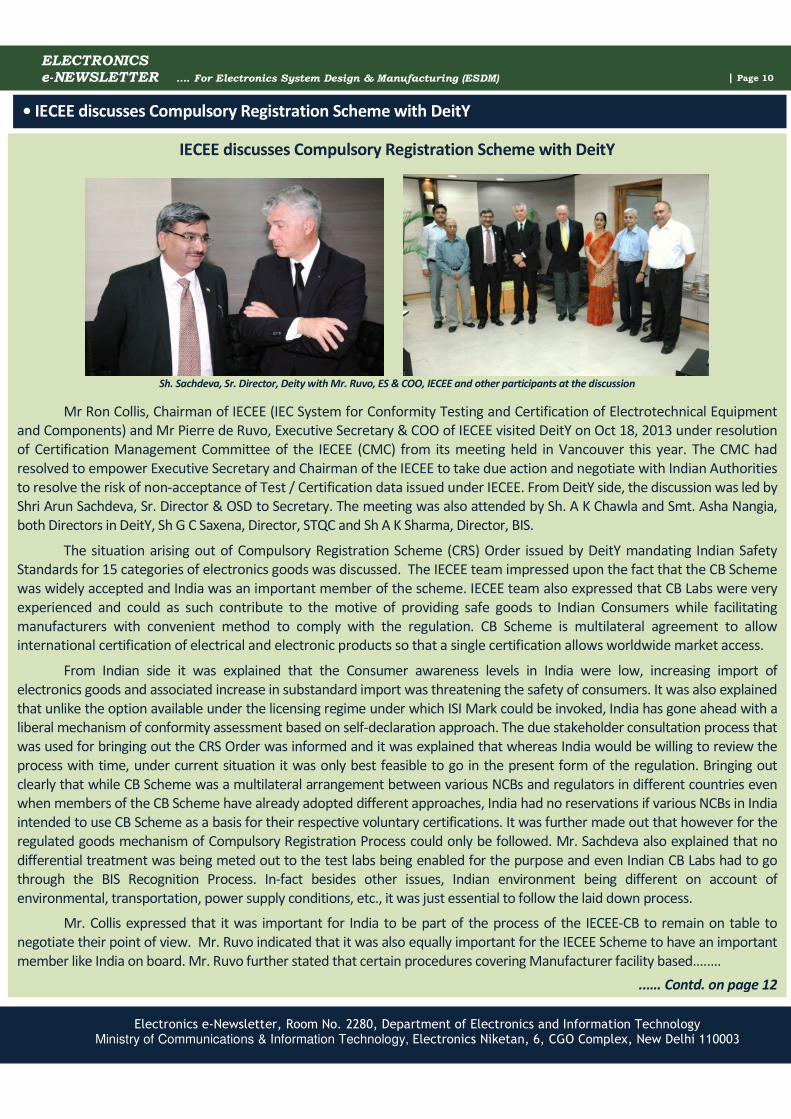
Sh. Sachdeva, Sr. Director, Deity with Mr. Ruvo, ES & COO, IECEE and other participants at the discussion
Mr Ron Collis, Chairman of IECEE (IEC System for Conformity Testing and Certification of Electrotechnical Equipment
and Components) and Mr Pierre de Ruvo, Executive Secretary & COO of IECEE visited DeitY on Oct 18, 2013 under resolution
of Certification Management Committee of the IECEE (CMC) from its meeting held in Vancouver this year. The CMC had
resolved to empower Executive Secretary and Chairman of the IECEE to take due action and negotiate with Indian Authorities
to resolve the risk of non-acceptance of Test / Certification data issued under IECEE. From DeitY side, the discussion was led by
Shri Arun Sachdeva, Sr. Director & OSD to Secretary. The meeting was also attended by Sh. A K Chawla and Smt. Asha Nangia,
both Directors in DeitY, Sh G C Saxena, Director, STQC and Sh A K Sharma, Director, BIS.
The situation arising out of Compulsory Registration Scheme (CRS) Order issued by DeitY mandating Indian Safety
Standards for 15 categories of electronics goods was discussed. The IECEE team impressed upon the fact that the CB Scheme
was widely accepted and India was an important member of the scheme. IECEE team also expressed that CB Labs were very
experienced and could as such contribute to the motive of providing safe goods to Indian Consumers while facilitating
manufacturers with convenient method to comply with the regulation. CB Scheme is multilateral agreement to allow
international certification of electrical and electronic products so that a single certification allows worldwide market access.
From Indian side it was explained that the Consumer awareness levels in India were low, increasing import of
electronics goods and associated increase in substandard import was threatening the safety of consumers. It was also explained
that unlike the option available under the licensing regime under which ISI Mark could be invoked, India has gone ahead with a
liberal mechanism of conformity assessment based on self-declaration approach. The due stakeholder consultation process that
was used for bringing out the CRS Order was informed and it was explained that whereas India would be willing to review the
process with time, under current situation it was only best feasible to go in the present form of the regulation. Bringing out
clearly that while CB Scheme was a multilateral arrangement between various NCBs and regulators in different countries even
when members of the CB Scheme have already adopted different approaches, India had no reservations if various NCBs in India
intended to use CB Scheme as a basis for their respective voluntary certifications. It was further made out that however for the
regulated goods mechanism of Compulsory Registration Process could only be followed. Mr. Sachdeva also explained that no
differential treatment was being meted out to the test labs being enabled for the purpose and even Indian CB Labs had to go
through the BIS Recognition Process. In-fact besides other issues, Indian environment being different on account of
environmental, transportation, power supply conditions, etc., it was just essential to follow the laid down process.
Mr. Collis expressed that it was important for India to be part of the process of the IECEE-CB to remain on table to
negotiate their point of view. Mr. Ruvo indicated that it was also equally important for the IECEE Scheme to have an important
member like India on board. Mr. Ruvo further stated that certain procedures covering Manufacturer facility based........
..…. Contd. on page 12
• ESSCI to train 8500 persons under STAR scheme • Labs Recognized for Testing of Electronics Products
| Page 11
ELECTRONICS e-NEWSLETTER …. For Electronics System Design & Manufacturing (ESDM)
Electronics e-Newsletter, Room No. 2280, Department of Electronics and Information Technology Ministry of Communications & Information Technology, Electronics Niketan, 6, CGO Complex, New Delhi 110003
ESSCI to train 8500 persons under STAR scheme
Seventh Governing Council Meeting of Electronic Sector Skill Council of India (ESSCI) and the first AGM was held on
Sept. 23, 2013. Among others, a plan to train 8,500 trainees under STAR scheme up to March 2014 under the STAR scheme
was finalized.
The first ESSCI Training Programme for ‘TV Repair Technician’ was launched in Kolkata on Oct 21, 2013. It is being
conducted by Providers Skill Academy Pvt. Ltd., Chennai.
Further, ESSCI has completed occupational mapping for IT Hardware and Consumer Electronics and the study for
remaining 10 sub-sectors is in progress. Sub-committee on IT Hardware has met twice and has identified 15 job roles and 15
National Occupational Standards (NOS) are under preparation. For Consumer Electronics, occupational mapping report has been
received. It is to be reviewed by a Sub-committee for Consumer Electronics.
ESSCI has also signed an MOU with Kerala State Govt. on Sept 24, 2013 for Skill development in PCB related courses.
Shri Ajai Chowdhry, Chairman, ESSCI also made a presentation to Shri Jairam Ramesh, Minister for Rural Development
Ministry on Oct 8, 2013. The Minister appreciated in the skill development plan of ESSCI, particularly the self employment in
rural areas. Based on the feedback, ESSCI is also planning to add an entrepreneurship module in related training programmes.
For more details, please contact Shri Pradeep Doshi, ESSCI (Email: [email protected]).
Labs Recognized for Testing of Electronics Products
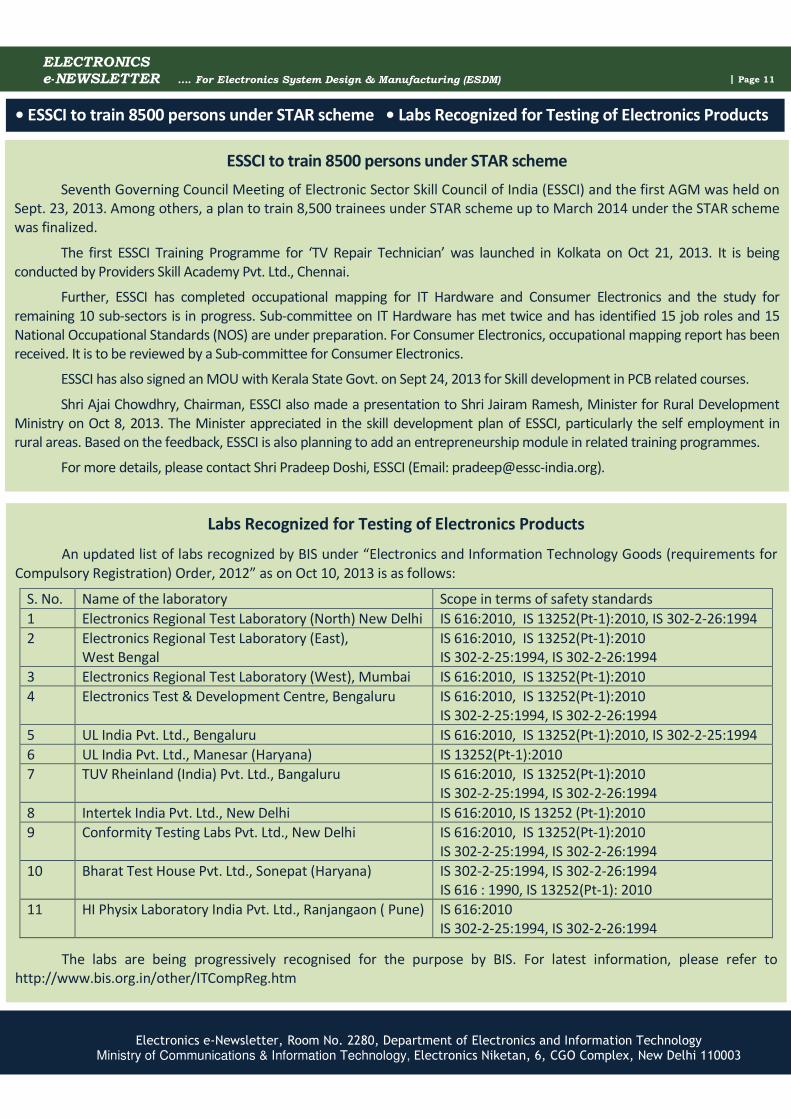
An updated list of labs recognized by BIS under “Electronics and Information Technology Goods (requirements for
Compulsory Registration) Order, 2012” as on Oct 10, 2013 is as follows:
S. No. Name of the laboratory Scope in terms of safety standards
1 Electronics Regional Test Laboratory (North) New Delhi IS 616:2010, IS 13252(Pt-1):2010, IS 302-2-26:1994
2 Electronics Regional Test Laboratory (East),
West Bengal
IS 616:2010, IS 13252(Pt-1):2010
IS 302-2-25:1994, IS 302-2-26:1994
3 Electronics Regional Test Laboratory (West), Mumbai IS 616:2010, IS 13252(Pt-1):2010
4 Electronics Test & Development Centre, Bengaluru IS 616:2010, IS 13252(Pt-1):2010
IS 302-2-25:1994, IS 302-2-26:1994
5 UL India Pvt. Ltd., Bengaluru IS 616:2010, IS 13252(Pt-1):2010, IS 302-2-25:1994
6 UL India Pvt. Ltd., Manesar (Haryana) IS 13252(Pt-1):2010
7 TUV Rheinland (India) Pvt. Ltd., Bangaluru IS 616:2010, IS 13252(Pt-1):2010
IS 302-2-25:1994, IS 302-2-26:1994
8 Intertek India Pvt. Ltd., New Delhi IS 616:2010, IS 13252 (Pt-1):2010
9 Conformity Testing Labs Pvt. Ltd., New Delhi IS 616:2010, IS 13252(Pt-1):2010
IS 302-2-25:1994, IS 302-2-26:1994
10
Bharat Test House Pvt. Ltd., Sonepat (Haryana) IS 302-2-25:1994, IS 302-2-26:1994
IS 616 : 1990, IS 13252(Pt-1): 2010
11 HI Physix Laboratory India Pvt. Ltd., Ranjangaon ( Pune) IS 616:2010
IS 302-2-25:1994, IS 302-2-26:1994
The labs are being progressively recognised for the purpose by BIS. For latest information, please refer to
http://www.bis.org.in/other/ITCompReg.htm
• CEAMA’s Conference on Flat Panel TVs Organized
| Page 12
ELECTRONICS e-NEWSLETTER …. For Electronics System Design & Manufacturing (ESDM)
Electronics e-Newsletter, Room No. 2280, Department of Electronics and Information Technology Ministry of Communications & Information Technology, Electronics Niketan, 6, CGO Complex, New Delhi 110003
CEAMA’s Conference on Flat Panel TVs Organized
Lighting of lamp and Dignitaries at the dais
CEAMA organized an International Conference on “Emerging Trends in Flat Panel TVs” on Oct 22, 2013 at New Delhi.
Shri J. Satyanarayana, IAS, Secretary, Department of Electronics & IT, was the chief guest for the conference. The conference
discussed on progressive steps to find practical solutions that will result in the creation of a long-term, sustainable
investment model and will prepare the Industry for technological advancements taking place in Flat Panel TV Segment.
Eminent Speakers included the Policy makers, Senior Government officials, distinguished personalities of international repute
and Indian Electronic Industry leaders.
Secretary, DeitY told, in his address, that there is ample opportunity in the sector of consumer electronics and the
industry need to come forward with new projects and investments and avail GOI incentives. Shri Satyanarayana released the
research report on “Emerging Trends in Flat Panel TVs” prepared by CEAMA & Frost & Sullivan. Dr. Ajay Kumar, Joint
Secretary, DeitY also spoke on the occasion.
According to CEAMA, LCD/LED TV Segment has been growing rapidly for last five years and will completely be
replacing CRT TVs in next 3-4 years. There are many technological advancement taking place in Flat Panel TV Segment such
as introduction of OLED TVs and ultra High Definition TVs, which would prepare the Indian Consumer Electronic Industry to
plan the development & manufacturing of next generation of Flat Panel TVs and explore greater value addition in the
country. All these developments will certainly enhance the viewing pleasure of consumers.
Mr. Anirudh Dhoot, President, CEAMA & Director, Videocon Industries, Mr. Manish Sharma, Managing Director,
Panasonic India, Mr. H.C Hung, Vice President, AUO, Mr. Rishi Tandan, Marketing Head, LG Electronics, Mr. Niju V,
Director, Frost & Sullivan, Mr. Indrajit Ghosh, Director, Display Search and Mr. Sunil Khandkar, Director, Samsung Asia
also spoke at the event.
….. Contd. from page 10.
……. testing to which India had also raised formal reservations, were set to be taken up in future meetings of the IECEE.
Indian Side explained that India was appreciative of the efforts being made under the IECEE. It was indicated that India had
already been accepting IECEE-CB Test Report for granting temporary registration and interim extensions to applicants under CRS. It
was only a considered view from Indian perspective that CB Certified Safety Critical Components for the notified goods were being
accepted for the purpose of Compulsory Registration even setting aside the requirements to have ISI Mark under licensing Scheme
of the Bureau of Indian Standards and even when Indian Standards were still at variance with the IEC ones.
While agreeing to that there was no infringement of the IECEE Rules and procedures by India, the visiting IECEE team
stated that the inputs gathered during the meeting would help them dispel the false notions that were growing in the International
Community with respect to India’s stand on this Order. The meeting concluded to work further to see that India’s participation in
the IECEE-CB increases with time.
• SEZ Units allowed to sub-contract production to DTA units • HES Exemptions from CRS
| Page 13
ELECTRONICS e-NEWSLETTER …. For Electronics System Design & Manufacturing (ESDM)
Electronics e-Newsletter, Room No. 2280, Department of Electronics and Information Technology Ministry of Communications & Information Technology, Electronics Niketan, 6, CGO Complex, New Delhi 110003
SEZ Units allowed to sub-contract to DTA units for upto 3 yrs
Department of Commerce, Ministry of Commerce & Industry,
Government of India vide its order October 11, 2013 has allowed sub-
contracting of production or any production process by large
manufacturing SEZ Units to Domestic Tariff Area (DTA) units for a period
up to 3 years at a stretch, instead of giving it on annual basis. For
availing this permission, following conditions have to be observed:
a. The SEZ unit should be a manufacturing unit (not including
Gems & Jewellery Sector units.
b. Such a unit should have substantial exports with average annual
exports of Rs. 1000 Crore or more in at least two out of four
years (i.e., current plus previous three years)
c. The unit should have been Net Foreign Exchange Earner over
the past 5 years block.
d. The unit should have an annual average export of not less than
51% of its total turnover in the block of 5 years.
e. The Unit should have an un-blemished track record and no
penalties against the unit for any violations under the Customs
Act, FTDR Act etc., should have been imposed.
f. The Bond-cum LUT signed by the SEZ unit should adequately
cover the goods which leave the SEZ for sub-contracting.
g. The period for which sub-contracting is allowed will not exceed
the validity period of the LOP of the SEZ unit.
h. The DTA unit to which the sub contract is to be awarded should
be registered with the Central Excise Department.
i. No Sub-contracting should be permitted for goods which are
restricted/prohibited or otherwise not permitted under any
provision of the SEZ Act and Rules.
j. Sub-contracting would also not ordinarily be permitted for
goods which attract anti-dumping duty as per EXIM Policy.
k. Such permission should be granted with the approval of the
Development Commissioner SEZ.
A copy of the order is available at www.deity.gov.in/esdm.
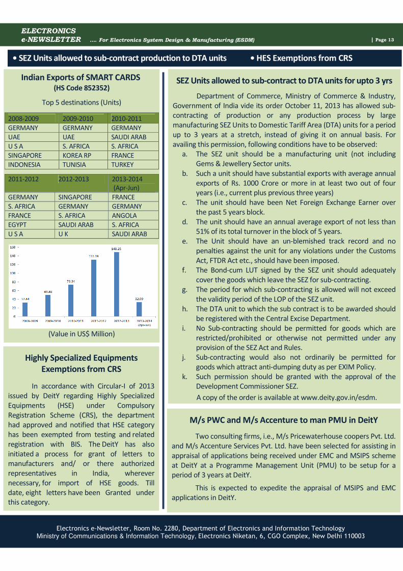
Indian Exports of SMART CARDS (HS Code 852352)
Top 5 destinations (Units)
2008-2009 2009-2010 2010-2011
GERMANY GERMANY GERMANY
UAE UAE SAUDI ARAB
U S A S. AFRICA S. AFRICA
SINGAPORE KOREA RP FRANCE
INDONESIA TUNISIA TURKEY
2011-2012 2012-2013 2013-2014
(Apr-Jun)
GERMANY SINGAPORE FRANCE
S. AFRICA GERMANY GERMANY
FRANCE S. AFRICA ANGOLA
EGYPT SAUDI ARAB S. AFRICA
U S A U K SAUDI ARAB
(Value in US$ Million)
Highly Specialized Equipments
Exemptions from CRS
In accordance with Circular-I of 2013
issued by DeitY regarding Highly Specialized
Equipments (HSE) under Compulsory
Registration Scheme (CRS), the department
had approved and notified that HSE category
has been exempted from testing and related
registration with BIS. The DeitY has also
initiated a process for grant of letters to
manufacturers and/ or there authorized
representatives in India, wherever
necessary, for import of HSE goods. Till
date, eight letters have been Granted under
this category.
M/s PWC and M/s Accenture to man PMU in DeitY
Two consulting firms, i.e., M/s Pricewaterhouse coopers Pvt. Ltd.
and M/s Accenture Services Pvt. Ltd. have been selected for assisting in
appraisal of applications being received under EMC and MSIPS scheme
at DeitY at a Programme Management Unit (PMU) to be setup for a
period of 3 years at DeitY.
This is expected to expedite the appraisal of MSIPS and EMC
applications in DeitY.
Published by: Department of Electronics and Information Technology, Ministry of Communications & Information Technology
Electronics Niketan, 6, CGO Complex, New Delhi 110003
| Page 14 ELECTRONICS
e-NEWSLETTER …. For Electronics System Design & Manufacturing (ESDM)
• FDI in excess of 26% allowed in Defence Production • Status of MSIPS Applications
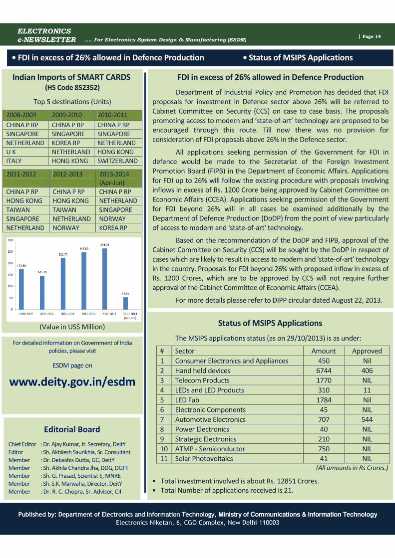
FDI in excess of 26% allowed in Defence Production
Department of Industrial Policy and Promotion has decided that FDI
proposals for investment in Defence sector above 26% will be referred to
Cabinet Committee on Security (CCS) on case to case basis. The proposals
promoting access to modern and ‘state-of-art’ technology are proposed to be
encouraged through this route. Till now there was no provision for
consideration of FDI proposals above 26% in the Defence sector.
All applications seeking permission of the Government for FDI in
defence would be made to the Secretariat of the Foreign Investment
Promotion Board (FIPB) in the Department of Economic Affairs. Applications
for FDI up to 26% will follow the existing procedure with proposals involving
inflows in excess of Rs. 1200 Crore being approved by Cabinet Committee on
Economic Affairs (CCEA). Applications seeking permission of the Government
for FDI beyond 26% will in all cases be examined additionally by the
Department of Defence Production (DoDP) from the point of view particularly
of access to modern and 'state-of-art' technology.
Based on the recommendation of the DoDP and FIPB, approval of the
Cabinet Committee on Security (CCS) will be sought by the DoDP in respect of
cases which are likely to result in access to modern and 'state-of-art' technology
in the country. Proposals for FDI beyond 26% with proposed inflow in excess of
Rs. 1200 Crores, which are to be approved by CCS will not require further
approval of the Cabinet Committee of Economic Affairs (CCEA).
For more details please refer to DIPP circular dated August 22, 2013.
Editorial Board
Chief Editor : Dr. Ajay Kumar, Jt. Secretary, DeitY
Editor : Sh. Akhilesh Saurikhia, Sr. Consultant
Member : Dr. Debashis Dutta, GC, DeitY
Member : Sh. Akhila Chandra Jha, DDG, DGFT
Member : Sh. G. Prasad, Scientist E, MNRE
Member : Sh. S.K. Marwaha, Director, DeitY
Member : Dr. R. C. Chopra, Sr. Advisor, CII
For detailed information on Government of India
policies, please visit
ESDM page on
www.deity.gov.in/esdm
Status of MSIPS Applications
The MSIPS applications status (as on 29/10/2013) is as under:
# Sector Amount Approved
1 Consumer Electronics and Appliances 450 Nil
2 Hand held devices 6744 406
3 Telecom Products 1770 NIL
4 LEDs and LED Products 310 11
5 LED Fab 1784 Nil
6 Electronic Components 45 NIL
7 Automotive Electronics 707 544
8 Power Electronics 40 NIL
9 Strategic Electronics 210 NIL
10 ATMP - Semiconductor 750 NIL
11 Solar Photovoltaics 41 NIL
(All amounts in Rs Crores.)
• Total investment involved is about Rs. 12851 Crores.
• Total Number of applications received is 21.
Indian Imports of SMART CARDS (HS Code 852352)
Top 5 destinations (Units)
2008-2009 2009-2010 2010-2011
CHINA P RP CHINA P RP CHINA P RP
SINGAPORE SINGAPORE SINGAPORE
NETHERLAND KOREA RP NETHERLAND
U K NETHERLAND HONG KONG
ITALY HONG KONG SWITZERLAND
2011-2012 2012-2013 2013-2014
(Apr-Jun)
CHINA P RP CHINA P RP CHINA P RP
HONG KONG HONG KONG NETHERLAND
TAIWAN TAIWAN SINGAPORE
SINGAPORE NETHERLAND NORWAY
NETHERLAND NORWAY KOREA RP
(Value in US$ Million)