dual-phase, +0.6v to +3.3v output parallelable, average
TRANSCRIPT

General DescriptionThe MAX5065/MAX5067 dual-phase, PWM controllersprovide high-output-current capability in a compactpackage with a minimum number of external compo-nents. The MAX5065/MAX5067 utilize a dual-phase,average-current-mode control that enables optimal useof low RDS(ON) MOSFETs, eliminating the need for exter-nal heatsinks even when delivering high output currents.
Differential sensing enables accurate control of the out-put voltage, while adaptive voltage positioning providesoptimum transient response. An internal regulatorenables operation with input voltage ranges of +4.75V to+5.5V or +8V to +28V. The high switching frequency, upto 500kHz per phase, and dual-phase operation allowthe use of low-output inductor values and input capacitorvalues. This accommodates the use of PC board-embedded planar magnetics achieving superior reliabili-ty, current sharing, thermal management, compact size,and low system cost.
The MAX5065/MAX5067 also feature a clock input(CLKIN) for synchronization to an external clock, and aclock output (CLKOUT) with programmable phase delay(relative to CLKIN) for paralleling multiple phases. TheMAX5065/MAX5067 also limit the reverse current if thebus voltage becomes higher than the regulated outputvoltage. These devices are specifically designed to limitcurrent sinking when multiple power-supply modules areparalleled. The MAX5065 offers an adjustable +0.6V to+3.3V output voltage. The MAX5067 output voltage isadjustable from +0.8V to +3.3V and features an overvolt-age protection and a power-good output signal.
The MAX5065/MAX5067 operate over the extendedtemperature range (-40°C to +85°C). The MAX5065 isavailable in a 28-pin SSOP package. The MAX5067 isavailable in a 44-pin thin QFN package. Refer to theMAX5037A data sheet for a VRM 9.0/VRM 9.1-compati-ble, VID-controlled output voltage controller in a 44-pinQFN package.
ApplicationsServers and Workstations
Point-of-Load High-Current/High-DensityTelecom DC-DC Regulators
Networking Systems
Large-Memory Arrays
RAID Systems
High-End Desktop Computers
Features +4.75V to +5.5V or +8V to +28V Input Voltage
Range
Adjustable VOUT+0.6V to +3.3V (MAX5065)+0.8V to +3.3V (MAX5067)
Up to 60A Output Current
Internal Voltage Regulator for a +12V or +24VPower Bus
Programmable Adaptive Output VoltagePositioning
True Differential Remote Output Sensing
Out-of-Phase Controllers Reduce InputCapacitance Requirement and Distribute PowerDissipation
Average-Current-Mode ControlSuperior Current Sharing Between IndividualPhases and Paralleled Modules
Accurate Current Limit Eliminates MOSFET andInductor Derating
Limits Reverse-Current Sinking in ParalleledModules
Integrated 4A Gate Drivers Selectable Fixed Frequency 250kHz or 500kHz Per
Phase (Up to 1MHz for Two Phases)
External Frequency Synchronization from 125kHzto 600kHz
Internal PLL with Clock Output for ParallelingMultiple DC-DC Converters
Thermal Protection
28-Pin SSOP Package (MAX5065)
44-Pin Thin QFN Package (MAX5067)
MA
X5
06
5/M
AX
50
67
Dual-Phase, +0.6V to +3.3V Output Parallelable,Average-Current-Mode Controllers
________________________________________________________________Maxim Integrated Products 1
19-3035; Rev 1; 11/03
For pricing, delivery, and ordering information, please contact Maxim/Dallas Direct! at 1-888-629-4642, or visit Maxim’s website at www.maxim-ic.com.
Ordering InformationPART TEMP RANGE PIN-PACKAGE
MAX5065EAI -40°C to +85°C 28 SSOP
MAX5067ETH -40°C to +85°C 44 Thin QFN
Selector Guide and Pin Configurations appear at end ofdata sheet.
MA
X5
06
5/M
AX
50
67
Dual-Phase, +0.6V to +3.3V Output Parallelable,Average-Current-Mode Controllers
2 _______________________________________________________________________________________
ABSOLUTE MAXIMUM RATINGS
ELECTRICAL CHARACTERISTICS(VCC = +5V, circuit of Figure 1, TA = -40°C to +85°C, unless otherwise noted. Typical specifications are at TA = +25°C.) (Note 1)
Stresses beyond those listed under “Absolute Maximum Ratings” may cause permanent damage to the device. These are stress ratings only, and functionaloperation of the device at these or any other conditions beyond those indicated in the operational sections of the specifications is not implied. Exposure toabsolute maximum rating conditions for extended periods may affect device reliability.
IN to SGND.............................................................-0.3V to +30VBST_ to SGND........................................................-0.3V to +35VDH_ to LX_ .................................-0.3V to [(VBST_ - VLX_) + 0.3V]DL_ to PGND..............................................-0.3V to (VCC + 0.3V)BST_ to LX_ ..............................................................-0.3V to +6VVCC to SGND............................................................-0.3V to +6VVCC, VDD to PGND ...................................................-0.3V to +6VSGND to PGND .....................................................-0.3V to +0.3VAll Other Pins to SGND...............................-0.3V to (VCC + 0.3V)
Continuous Power Dissipation (TA = +70°C)28-Pin SSOP (derate 9.5mW/°C above +70°C) ............762mW44-Pin Thin QFN (derate 27.0mW/°C above+70°C) ...2162mW
Operating Temperature Range ...........................-40°C to +85°CMaximum Junction Temperature .....................................+150°CStorage Temperature Range .............................-60°C to +150°CLead Temperature (soldering, 10s) .................................+300°C
PARAMETER SYMBOL CONDITIONS MIN TYP MAX UNITS
SYSTEM SPECIFICATIONS
8 28
Input Voltage Range VIN Short IN and VCC together for +5V inputoperation
4.75 5.50V
Quiescent Supply Current IQ EN = VCC or SGND 4 10 mA
Efficiency η ILOAD = 52A (26A per phase) 90 %
OUTPUT VOLTAGE
No load 0.5952 0.6 0.6048
MAX5065 No load, VCC = +4.75V to +5.5Vor VIN = +8V to +28V
0.594 0.6 0.6064
No load 0.7936 0.8 0.8064SENSE+ to SENSE- Accuracy(Note 4)
MAX5067 No load, VCC = +4.75V to +5.5Vor VIN = +8V to +28V
0.792 0.8 0.808
V
STARTUP/INTERNAL REGULATOR
VCC Undervoltage Lockout UVLO VCC rising 4.0 4.15 4.5 V
VCC Undervoltage LockoutHysteresis
200 mV
VCC Output Accuracy VIN = +8V to +28V, ISOURCE = 0 to 80mA 4.85 5.1 5.30 V
MOSFET DRIVERS
Output Driver Impedance RON Low or high output 1 3 Ω
Output Driver Source/SinkCurrent
IDH_, IDL_ 4 A
Nonoverlap Time tNO CDH_/DL_ = 5nF 60 ns
OSCILLATOR AND PLL
CLKIN = SGND 238 250 262Switching Frequency fSW
CLKIN = VCC 475 500 525kHz
PLL Lock Range fPLL 125 600 kHz
PLL Locking Time tPLL 200 µs
MA
X5
06
5/M
AX
50
67
Dual-Phase, +0.6V to +3.3V Output Parallelable,Average-Current-Mode Controllers
_______________________________________________________________________________________ 3
ELECTRICAL CHARACTERISTICS (continued)(VCC = +5V, circuit of Figure 1, TA = -40°C to +85°C, unless otherwise noted. Typical specifications are at TA = +25°C.) (Note 1)
PARAMETER SYMBOL CONDITIONS MIN TYP MAX UNITS
PHASE = VCC 115 120 125
PHASE = unconnected 85 90 95CLKOUT Phase Shift(At fSW = 125kHz)
φCLKOUT
PHASE = SGND 55 60 65
degrees
CLKIN Input Pulldown Current ICLKIN 3 5 7 µA
CLKIN High Threshold VCLKINH 2.4 V
CLKIN Low Threshold VCLKINL 0.8 V
CLKIN High Pulse Width tCLKIN 200 ns
PHASE High Threshold VPHASEH 4 V
PHASE Low Threshold VPHASEL 1 V
PHASE Input Bias Current IPHASEBIAS -50 +50 µA
CLKOUT Output Low Level VCLKOUTL ISINK = 2mA (Note 2) 100 mV
CLKOUT Output High Level VCLKOUTH ISOURCE = 2mA (Note 2) 4.5 V
CURRENT LIMIT
Average Current-Limit Threshold VCL CSP_ to CSN_ 45 48 51 mV
Reverse Current-Limit Threshold VCLR CSP_ to CSN_ -3.9 -0.2 mV
Cycle-by-Cycle Current Limit VCLPK CSP_ to CSN_ (Note 3) 90 112 130 mV
Cycle-by-Cycle OverloadResponse Time
tR VCSP_ to VCSN_ = +150mV 260 ns
CURRENT-SENSE AMPLIFIER
CSP_ to CSN_ Input Resistance RCS_ 4 kΩ
Common-Mode Range VCMR(CS) -0.3 +3.6 V
Input Offset Voltage VOS(CS) -1 +1 mV
Amplifier Gain AV(CS) 18 V/V
3dB Bandwidth f3dB 4 MHz
CURRENT-ERROR AMPLIFIER (TRANSCONDUCTANCE AMPLIFIER)
Transconductance gmca 550 µS
Open-Loop Gain AVOL(CE) No load 50 dB
DIFFERENTIAL VOLTAGE AMPLIFIER (DIFF)
Common-Mode Voltage Range VCMR(DIFF) -0.3 +1.0 V
DIFF Output Voltage VCM VSENSE+ = VSENSE- = 0 0.6 V
Input Offset Voltage VOS(DIFF) -1 +1 mV
Amplifier Gain AV(DIFF) 0.997 1 1.003 V/V
3dB Bandwidth f3dB CDIFF = 20pF 3 MHz
Minimum Output Current Drive IOUT(DIFF) 1.0 mA
SENSE+ to SENSE- InputResistance
RVS_ 50 100 kΩ
MA
X5
06
5/M
AX
50
67
Dual-Phase, +0.6V to +3.3V Output Parallelable,Average-Current-Mode Controllers
4 _______________________________________________________________________________________
ELECTRICAL CHARACTERISTICS (continued)(VCC = +5V, circuit of Figure 1, TA = -40°C to +85°C, unless otherwise noted. Typical specifications are at TA = +25°C.) (Note 1)
PARAMETER SYMBOL CONDITIONS MIN TYP MAX UNITS
VOLTAGE-ERROR AMPLIFIER (EAOUT)
Open-Loop Gain AVOL(EA) 70 dB
Unity-Gain Bandwidth fUGEA 3 MHz
EAN Input Bias Current IB(EA) VEAN = +2.0V -100 +100 nA
Error-Amplifier Output ClampingVoltage
VCLAMP(EA) With respect to VCM 810 918 mV
POWER-GOOD, PHASE FAILURE DETECTION, OVERVOLTAGE PROTECTION, AND THERMAL SHUTDOWN
VOVPGOOD goes low when VOUT is outside thiswindow
+6 +8 +10
PGOOD Trip Level (MAX5067)
VUVPGOOD goes low when VOUT is outside thiswindow
-12.5 -10 -8.5
%VOUT
PGOOD Output Low Level(MAX5067)
VPGLO ISINK = 4mA 0.2 V
PGOOD Output Leakage Current(MAX5067)
IPG PGOOD = VCC 1 µA
Phase Failure Trip Threshold(MAX5067)
VPHPGOOD goes low when CLP_ is higherthan VPH
2 V
OVPIN Trip Threshold (MAX5067) OVPTH With respect to SGND 0.792 0.8 0.808 V
OVPIN Input Resistance(MAX5067)
ROVPIN 190 280 370 kΩ
THERMAL SHUTDOWN
Thermal Shutdown TSHDN 150 °C
Thermal-Shutdown Hysteresis 8 °C
EN INPUT
EN Input Low Voltage VENL 1 V
EN Input High Voltage VENH 3 V
EN Pullup Current IEN 4.5 5 5.5 µA
Note 1: Specifications from -40°C to 0°C are guaranteed by characterization but not production tested.Note 2: Guaranteed by design. Not production tested.Note 3: See Peak-Current Comparator section.Note 4: Does not include an error due to finite error amplifier gain. See the Voltage-Error Amplifier section.
MA
X5
06
5/M
AX
50
67
Dual-Phase, +0.6V to +3.3V Output Parallelable,Average-Current-Mode Controllers
_______________________________________________________________________________________ 5
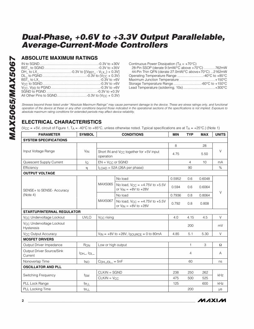
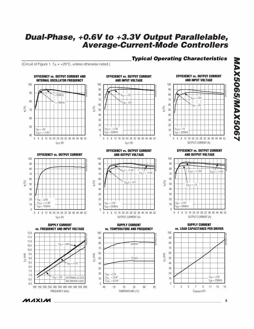
EFFICIENCY vs. OUTPUT CURRENT ANDINTERNAL OSCILLATOR FREQUENCY
MAX
5065
/67
toc0
1
IOUT (A)
η (%
)
4844403632282420161284
50
60
70
80
90
100
400 52
f = 500kHz
f = 250kHz
VIN = +5VVOUT = +1.8V
EFFICIENCY vs. OUTPUT CURRENTAND INPUT VOLTAGE
MAX
5065
/67
toc0
2
IOUT (A)
η (%
)
4844403632282420161284
50
40
30
20
10
60
70
80
90
100
00 52
VIN = +12V
VIN = +5V
VOUT = +1.8VfSW = 250kHz
EFFICIENCY vs. OUTPUT CURRENTAND INPUT VOLTAGE
MAX
5065
/67
toc0
3
OUTPUT CURRENT (A)
η (%
)
484436 4012 16 20 24 28 324 8
10
20
30
40
50
60
70
80
90
100
00 52
VIN = +12V
VIN = +5V
VOUT = 1VfSW = 250kHz
EFFICIENCY vs. OUTPUT CURRENT
MAX
5065
/67
toc0
4
IOUT (A)
η (%
)
4844403632282420161284
50
40
30
20
10
60
70
80
90
100
00 52
VIN = +24VVOUT = +1.8VfSW = 125kHz
EFFICIENCY vs. OUTPUT CURRENTAND OUTPUT VOLTAGE
MAX
5065
/67
toc0
5
OUTPUT CURRENT (A)
η (%
)
4844403632282420161284
50
40
30
20
10
60
70
80
90
100
00 52
VOUT = +1V
VOUT = +1.5VVOUT = +1.8V
VIN = +12VfSW = 250kHz
EFFICIENCY vs. OUTPUT CURRENTAND OUTPUT VOLTAGE
MAX
5065
/67
toc0
6
OUTPUT CURRENT (A)
η (%
)
4844403632282420161284
50
40
30
20
10
60
70
80
90
100
00 52
VOUT = +1V
VOUT = +1.5V VOUT = +1.8V
VIN = +12VfSW = 500kHz
SUPPLY CURRENTvs. FREQUENCY AND INPUT VOLTAGE
MAX
5065
/67
toc0
7
FREQUENCY (kHz)
I CC
(mA)
550500400 450200 250 300 350150
6.57.07.58.08.59.09.5
10.010.511.011.512.0
6.0100 600
VIN = +24V
VIN = +12V
VIN = +5V EXTERNALCLOCKNO DRIVER LOAD
SUPPLY CURRENTvs. TEMPERATURE AND FREQUENCY
MAX
5065
/67
toc0
8
TEMPERATURE (°C)
I CC
(mA)
603510-15
10
20
30
40
50
60
70
80
90
100
0-40 85
250kHz
125kHz
VIN = +12VCDL_ = 22nFCDH_ = 8.2nF
SUPPLY CURRENTvs. LOAD CAPACITANCE PER DRIVER
MAX
5065
/67
toc0
9
CDRIVER (nF)
I CC
(mA)
13117 953
10
20
30
40
50
60
70
80
90
100
01 15
VIN = +12VfSW = 250kHz
Typical Operating Characteristics(Circuit of Figure 1. TA = +25°C, unless otherwise noted.)
MA
X5
06
5/M
AX
50
67
Dual-Phase, +0.6V to +3.3V Output Parallelable,Average-Current-Mode Controllers
6 _______________________________________________________________________________________
Typical Operating Characteristics (continued)(Circuit of Figure 1, TA = +25°C, unless otherwise noted.)
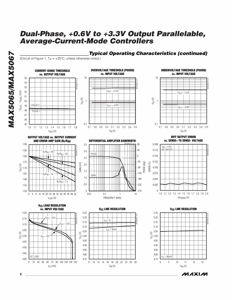
CURRENT-SENSE THRESHOLDvs. OUTPUT VOLTAGE
MAX
5065
/67
toc1
0
VOUT (V)
(VCS
P_ -
V CSN
_) (m
V)
1.71.61.4 1.51.2 1.31.1
46
47
48
49
50
51
52
53
54
55
451.0 1.8
PHASE 2
PHASE 1
10
0.14.7 4.8 4.9 5.0 5.1 5.2 5.3 5.4 5.5
OVERVOLTAGE THRESHOLD (PGOOD)vs. INPUT VOLTAGE
1
MAX
5065
/67
toc1
1
VIN (V)
V OV
(V)
VOUT = +0.8V
VOUT = +3.3V
10
4.7 4.8 4.9 5.0 5.1 5.2 5.3 5.4 5.5
UNDERVOLTAGE THRESHOLD (PGOOD)vs. INPUT VOLTAGE
1
0.1
MAX
5065
/67
toc1
2
VIN (V)
V UV
(V)
VOUT = +0.8V
VOUT = +3.3V
1.50
1.60
1.55
1.75
1.70
1.65
1.80
1.85
1.90
0 8 124 16 20 24 28 32 36 40 44 48 52
OUTPUT VOLTAGE vs. OUTPUT CURRENTAND ERROR AMP GAIN (RF/RIN)
MAX
5065
/67
toc1
3
ILOAD (A)
V OUT
(V)
RF/RIN = 40RF/RIN = 20
RF/RIN = 7.5
RF/RIN = 10
DIFFERENTIAL AMPLIFIER BANDWIDTHMAX5065/67 toc14
FREQUENCY (MHz)
GAIN
(V/V
)
PHAS
E (d
eg)
10.1
0.5
1.0
1.5
2.0
2.5
3.0
3.5
00.01 10
-225
-270
-180
-135
-90
-45
0
45
90
PHASE
GAIN
DIFF OUTPUT ERRORvs. SENSE+ TO SENSE- VOLTAGE
MAX
5065
/67
toc1
5
∆VSENSE (V)
ERRO
R (%
)
1.91.81.1 1.2 1.3 1.5 1.61.4 1.7
0.025
0.050
0.075
0.100
0.125
0.150
0.175
0.200
01.0 2.0
VIN = +12VNO DRIVER
VCC LOAD REGULATIONvs. INPUT VOLTAGE
MAX
5065
/67
toc1
6
ICC (mA)
V CC
(V)
13512015 30 45 75 9060 105
4.85
4.90
4.95
5.00
5.05
5.10
5.15
5.20
4.800 150
VIN = +24V
VIN = +12V
VIN = +8V
DC LOAD
VCC LINE REGULATION
MAX
5065
/67
toc1
7
VIN (V)
V CC
(V)
262420 2212 14 16 1810
4.80
4.85
4.90
4.95
5.00
5.05
5.10
5.15
5.20
5.25
4.758 28
ICC = 0
ICC = 40mA
VCC LINE REGULATIONM
AX50
65/6
7 to
c18
VIN (V)
V CC
(V)
13129 10 11
4.80
4.85
4.90
4.95
5.00
5.05
5.10
5.15
5.20
5.25
4.758
ICC = 80mA
MA
X5
06
5/M
AX
50
67
Dual-Phase, +0.6V to +3.3V Output Parallelable,Average-Current-Mode Controllers
_______________________________________________________________________________________ 7
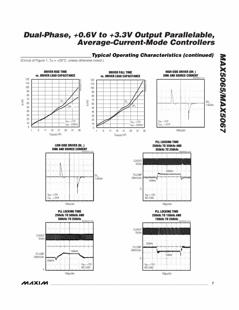
DRIVER RISE TIMEvs. DRIVER LOAD CAPACITANCE
MAX
5065
/67
toc1
9
CDRIVER (nF)
t R (n
s)
312616 21116
102030405060708090
100110120
01 36
DL_
DH_
VIN = +12VfSW = 250kHz
DRIVER FALL TIMEvs. DRIVER LOAD CAPACITANCE
MAX
5065
/67
toc2
0
CDRIVER (nF)
t R (n
s)
312616 21116
102030405060708090
100110120
01 36
DL_
DH_
VIN = +12VfSW = 250kHz
100ns/div
HIGH-SIDE DRIVER (DH_)SINK AND SOURCE CURRENT
DH_1.6A/div
MAX5065/67 toc21
VIN = +12VCDH_ = 22nF
100ns/div
LOW-SIDE DRIVER (DL_)SINK AND SOURCE CURRENT
DL_1.6A/div
MAX5065/67 toc22
VIN = +12VCDL_ = 22nF
100µs/div
PLL LOCKING TIME250kHz TO 350kHz AND
350kHz TO 250kHz
CLKOUT5V/div
MAX5065/67 toc23
PLLCMP200mV/div
VIN = +12VNO LOAD
350kHz
250kHz
0
100µs/div
PLL LOCKING TIME250kHz TO 500kHz AND
500kHz TO 250kHz
CLKOUT5V/div
MAX5065/67 toc24
PLLCMP200mV/div
0
VIN = +12VNO LOAD
500kHz
250kHz
100µs/div
PLL LOCKING TIME250kHz TO 150kHz AND
150kHz TO 250kHz
CLKOUT5V/div
MAX5065/67 toc25
PLLCMP200mV/div
0
VIN = +12VNO LOAD
250kHz
150kHz
Typical Operating Characteristics (continued)(Circuit of Figure 1, TA = +25°C, unless otherwise noted.)
MA
X5
06
5/M
AX
50
67
Dual-Phase, +0.6V to +3.3V Output Parallelable,Average-Current-Mode Controllers
8 _______________________________________________________________________________________
Typical Operating Characteristics (continued)(Circuit of Figure 1, TA = +25°C, unless otherwise noted.)
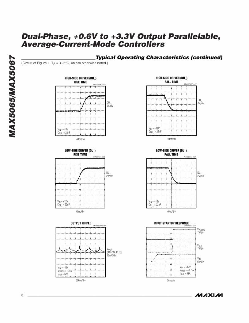
40ns/div
LOW-SIDE DRIVER (DL_)RISE TIME
MAX5065/67 toc28
DL_2V/div
VIN = +12VCDL_ = 22nF
40ns/div
LOW-SIDE DRIVER (DL_)FALL TIME
MAX5065/67 toc29
DL_2V/div
VIN = +12VCDL_ = 22nF
500ns/div
OUTPUT RIPPLEMAX5065/67 toc30
VOUT(AC-COUPLED)10mV/div
VIN = +12VVOUT = +1.75VIOUT = 52A
2ms/div
INPUT STARTUP RESPONSEMAX5065/67 toc31
VIN 5V/div
VIN = +12VVOUT = +1.75VIOUT = 52A
VPGOOD1V/div
VOUT1V/div
40ns/div
HIGH-SIDE DRIVER (DH_)RISE TIME
MAX5065/67 toc26
VIN = +12VCDH_ = 22nF
DH_2V/div
40ns/div
HIGH-SIDE DRIVER (DH_)FALL TIME
MAX5065/67 toc27
DH_2V/div
VIN = +12VCDH_ = 22nF

MA
X5
06
5/M
AX
50
67
Dual-Phase, +0.6V to +3.3V Output Parallelable,Average-Current-Mode Controllers
_______________________________________________________________________________________ 9
1ms/div
ENABLE STARTUP RESPONSEMAX5065/67 toc32
VEN 2V/div
VPGOOD1V/div
VOUT1V/div
VIN = +12VVOUT = +1.75VIOUT = 52A
40µs/div
LOAD-TRANSIENT RESPONSEMAX5065/67 toc33
VIN = +12VVOUT = +1.75VISTEP = 8A TO 52AtRISE = 1µs
VOUT50mV/div
REVERSE CURRENT SINKvs. TEMPERATURE
MAX
5065
/67
toc3
4
TEMPERATURE (°C)
I REV
ERSE
(A)
603510-15
2.4
2.5
2.6
2.7
2.8
2.3-40 85
VEXTERNAL = +3.3V
VEXTERNAL = +2V
VIN = +12VVOUT = 1.5V R1 = R2 = 1.5mΩ
200µs/div
REVERSE CURRENT SINK AT INPUT TURN-ON(VIN = 12V, VOUT = 1.5V, VEXTERNAL = 2.5V)
MAX5065/67 toc35
REVERSECURRENT5A/div0A
R1 = R2 = 1.5mΩ
200µs/div
REVERSE CURRENT SINK AT INPUT TURN-ON(VIN = 12V, VOUT = 1.5V, VEXTERNAL = 3.3V)
MAX5065/67 toc36
REVERSECURRENT10A/div
0A
R1 = R2 = 1.5mΩ
200µs/div
REVERSE CURRENT SINK AT ENABLE TURN-ON(VIN = 12V, VOUT = 1.5V, VEXTERNAL = 2.5V)
MAX5065/67 toc37
REVERSECURRENT5A/div
0A
R1 = R2 = 1.5mΩ
200µs/div
REVERSE CURRENT SINK AT ENABLE TURN-ON(VIN = 12V, VOUT = 1.5V, VEXTERNAL = 3.3V)
MAX5065/67 toc38
REVERSECURRENT10A/div
0A
R1 = R2 = 1.5mΩ
Typical Operating Characteristics (continued)(Circuit of Figure 1, TA = +25°C, unless otherwise noted.)
MA
X5
06
5/M
AX
50
67
Dual-Phase, +0.6V to +3.3V Output Parallelable,Average-Current-Mode Controllers
10 ______________________________________________________________________________________
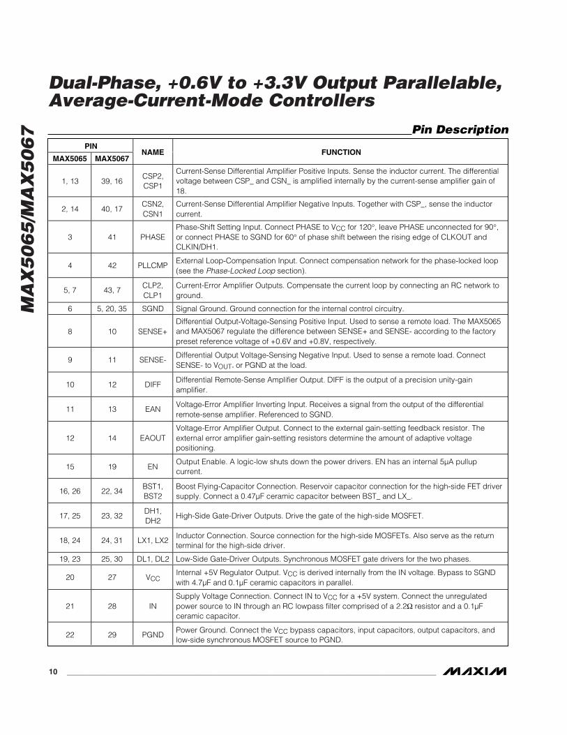
Pin DescriptionPIN
MAX5065 MAX5067NAME FUNCTION
1, 13 39, 16CSP2,CSP1
Current-Sense Differential Amplifier Positive Inputs. Sense the inductor current. The differentialvoltage between CSP_ and CSN_ is amplified internally by the current-sense amplifier gain of18.
2, 14 40, 17CSN2,CSN1
Current-Sense Differential Amplifier Negative Inputs. Together with CSP_, sense the inductorcurrent.
3 41 PHASEPhase-Shift Setting Input. Connect PHASE to VCC for 120°, leave PHASE unconnected for 90°,or connect PHASE to SGND for 60° of phase shift between the rising edge of CLKOUT andCLKIN/DH1.
4 42 PLLCMPExternal Loop-Compensation Input. Connect compensation network for the phase-locked loop(see the Phase-Locked Loop section).
5, 7 43, 7CLP2,CLP1
Current-Error Amplifier Outputs. Compensate the current loop by connecting an RC network toground.
6 5, 20, 35 SGND Signal Ground. Ground connection for the internal control circuitry.
8 10 SENSE+Differential Output-Voltage-Sensing Positive Input. Used to sense a remote load. The MAX5065and MAX5067 regulate the difference between SENSE+ and SENSE- according to the factorypreset reference voltage of +0.6V and +0.8V, respectively.
9 11 SENSE-Differential Output Voltage-Sensing Negative Input. Used to sense a remote load. ConnectSENSE- to VOUT- or PGND at the load.
10 12 DIFFDifferential Remote-Sense Amplifier Output. DIFF is the output of a precision unity-gainamplifier.
11 13 EANVoltage-Error Amplifier Inverting Input. Receives a signal from the output of the differentialremote-sense amplifier. Referenced to SGND.
12 14 EAOUTVoltage-Error Amplifier Output. Connect to the external gain-setting feedback resistor. Theexternal error amplifier gain-setting resistors determine the amount of adaptive voltagepositioning.
15 19 ENOutput Enable. A logic-low shuts down the power drivers. EN has an internal 5µA pullupcurrent.
16, 26 22, 34BST1,BST2
Boost Flying-Capacitor Connection. Reservoir capacitor connection for the high-side FET driversupply. Connect a 0.47µF ceramic capacitor between BST_ and LX_.
17, 25 23, 32DH1,DH2
High-Side Gate-Driver Outputs. Drive the gate of the high-side MOSFET.
18, 24 24, 31 LX1, LX2Inductor Connection. Source connection for the high-side MOSFETs. Also serve as the returnterminal for the high-side driver.
19, 23 25, 30 DL1, DL2 Low-Side Gate-Driver Outputs. Synchronous MOSFET gate drivers for the two phases.
20 27 VCCInternal +5V Regulator Output. VCC is derived internally from the IN voltage. Bypass to SGNDwith 4.7µF and 0.1µF ceramic capacitors in parallel.
21 28 INSupply Voltage Connection. Connect IN to VCC for a +5V system. Connect the unregulatedpower source to IN through an RC lowpass filter comprised of a 2.2Ω resistor and a 0.1µFceramic capacitor.
22 29 PGNDPower Ground. Connect the VCC bypass capacitors, input capacitors, output capacitors, andlow-side synchronous MOSFET source to PGND.

MA
X5
06
5/M
AX
50
67
Dual-Phase, +0.6V to +3.3V Output Parallelable,Average-Current-Mode Controllers
______________________________________________________________________________________ 11
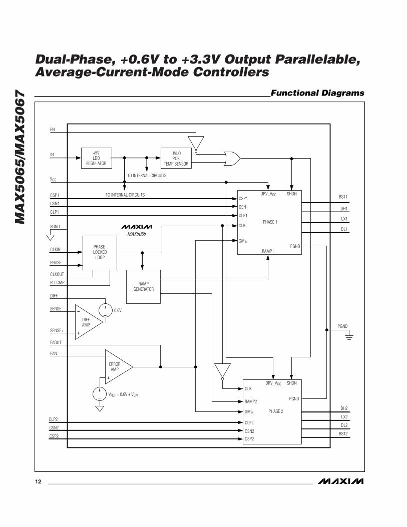
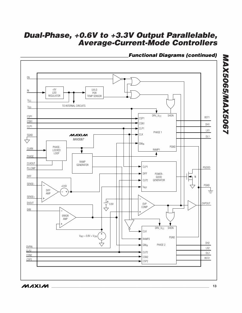
Detailed DescriptionThe MAX5065/MAX5067 average-current-mode PWMcontrollers drive two out-of-phase buck converter chan-nels. Average-current-mode control improves currentsharing between the channels while minimizing compo-nent derating and size. Parallel multiple MAX5065/MAX5067 regulators to increase the output currentcapacity. For maximum ripple rejection at the input, setthe phase shift between phases to 90° for two paral-leled converters, or 60° for three paralleled converters.Paralleling the MAX5065/MAX5067s improves designflexibility in applications requiring upgrades (higherload).
Dual-phase converters with an out-of-phase lockingarrangement reduce the input and output capacitor ripple current, effectively multiplying the switching fre-quency by the number of phases. Each phase of theMAX5065/MAX5067 consists of an inner average cur-rent loop controlled by a common outer-loop voltage-error amplifier (VEA). The combined action of the twoinner current loops and the outer voltage loop correctsthe output voltage errors and forces the phase currentsto be equal. Program the output voltage from +0.6V to
+3.3V (MAX5065) and +0.8V to +3.3V (MAX5067) usinga resistive-divider at SENSE+ and SENSE-.
VIN, VCC, VDD The MAX5065/MAX5067 accept a wide input voltagerange of +4.75V to +5.5V or +8V to +28V. All internalcontrol circuitry operates from an internally regulatednominal voltage of +5V (VCC). For input voltages of +8Vor greater, the internal VCC regulator steps the voltagedown to +5V. The VCC output voltage regulates to +5Vwhile sourcing up to 80mA. Bypass VCC to SGND with4.7µF and 0.1µF low-ESR ceramic capacitors for high-frequency noise rejection and stable operation (Figures1, 2, and 3).
Calculate power dissipation in the MAX5065/MAX5067as a product of the input voltage and the total VCC reg-ulator output current (ICC). ICC includes quiescent cur-rent (IQ) and gate-drive current (IDD):
PD = VIN x ICC
ICC = IQ + fSW x (QG1 + QG2 + QG3 + QG4)
Pin Description (continued)PIN
MAX5065 MAX5067NAME FUNCTION
27 36 CLKOUTOscillator Output. CLKOUT is phase-shifted from CLKIN by the amount determined by thePHASE input. Use CLKOUT to parallel additional MAX5065/MAX5067s.
28 38 CLKIN
CMOS Logic Clock Input. Drive CLKIN with a frequency range between 125kHz and 600kHz orconnect to VCC or SGND. Connect CLKIN to SGND to set the internal oscillator to 250kHz orconnect to VCC to set the internal oscillator to 500kHz. CLKIN has an internal 5µA pulldowncurrent.
— 6 OVPINOvervoltage Protection Circuit Input. Connect OVPIN to the center of the resistive-dividerbetween VOUT and GND. When OVPIN exceeds +0.8V with respect to SGND, OVPOUT latchesDH_ low and DL_ high. Toggle EN low to high or recycle the power to reset the latch.
— 8 OVPOUTOvervoltage Protection Output. Use the OVPOUT active-high, push-pull output to trigger asafety device such as an SCR.
— 9 PGOOD
Power-Good Output. The open-drain, active-low PGOOD output goes low when the outputvoltage falls out of regulation or a phase failure is detected. The power-good window-comparator thresholds are +8% and -10% of the output voltage. Forcing EN low also forcesPGOOD low.
—
1, 2, 3, 4,15, 18,21, 33,37, 44
N.C. No Connection. Not internally connected.
— 26 VDD
Supply Voltage for Low-Side and High-Side Drivers. VCC powers VDD. Connect a parallelcombination of 0.1µF and 1µF ceramic capacitors to PGND and a 1Ω resistor to VCC to filterout the high peak currents of the driver from the internal circuitry.
(1)
(2)
MA
X5
06
5/M
AX
50
67
Dual-Phase, +0.6V to +3.3V Output Parallelable,Average-Current-Mode Controllers
12 ______________________________________________________________________________________
MAX5065
IN
EN
PHASE 1
CSP1DRV_VCC
RAMP1
GMIN
CLK
CLP1
CSN1
SHDNBST1
DL1
LX1
DH1
VCC
TO INTERNAL CIRCUITS
TO INTERNAL CIRCUITS
CSP1
CSN1
CLP1
PHASE 2
CSP2
DRV_VCC
GMIN
CLK
CLP2
CSN2
SHDN
BST2
DL2
LX2
DH2
CSP2
CSN2
CLP2
PHASE-LOCKED
LOOP
RAMPGENERATOR
RAMP2
CLKIN
PHASE
CLKOUT
PLLCMP
DIFFAMP
ERRORAMP
SENSE-
SENSE+
DIFF
EAN
EAOUT
PGND
PGND
PGND
SGND
VREF = 0.6V + VCM
+5VLDO
REGULATOR
UVLOPOR
TEMP SENSOR
0.6V
Functional Diagrams
MA
X5
06
5/M
AX
50
67
Dual-Phase, +0.6V to +3.3V Output Parallelable,Average-Current-Mode Controllers
______________________________________________________________________________________ 13
MAX5067
IN
EN
PHASE 1
CSP1DRV_VCC
RAMP1
GMIN
CLK
CLP1
CSN1
SHDNBST1
DL1
LX1
DH1
VCC
VDDTO INTERNAL CIRCUITS
CSP1
CSN1
CLP1
PHASE 2
CSP2
DRV_VCC
GMIN
CLK
CLP2
CSN2
SHDN
BST2
DL2
LX2
DH2
OVPOUT
PGOOD
CSP2
CSN2
CLP2OVPIN
PHASE-LOCKED
LOOP
RAMPGENERATOR
RAMP2
POWER-GOOD
GENERATORCLP2
CLP1
VREF
DIFF
CLKIN
PHASE
CLKOUT
PLLCMP
DIFFAMP
ERRORAMP
SENSE-
SENSE+
DIFF
EAN
EAOUT
PGND
PGND
PGND
SGND
VREF = 0.8V + VCM
+5VLDO
REGULATOR
UVLOPOR
TEMP SENSOR
+0.6V
0.8V OVPCOMP
N
Functional Diagrams (continued)
MA
X5
06
5/M
AX
50
67
Dual-Phase, +0.6V to +3.3V Output Parallelable,Average-Current-Mode Controllers
14 ______________________________________________________________________________________
MAX
5067
Q4Q3
C39
C40
R3
D2
Q2
D1
V IN
C8 C11
Q1
V IN
V CC
D4D3
C41
C12
C38
C3–C
7
C14
C15
C16
C25
C26,
C30,
C37
LOAD
L2R2
L1R1
DH1
LX1
DL1
BST1 V D
D
V CC
DH2
LX2
DL2
BST2
CSP2
CSN2
PGOO
DPH
ASE
SGND
PGND
CLP2
CLP1
R11
PGOO
DV C
C
R6
C35
C36
R5 C33
C34
C42
C1, C
2
R13
V CC
C31
C32
R4
CSP1
CSN1
SENS
E+SE
NSE-
INCL
KIN
PLLC
MP
EN
R fR IN
R12
C43
V IN
EAOU
T
EAN
DIFF
OVPI
N
OVPO
UT
C13
IN
IN
C44
RA RB
RH RL
V CC
R X
V OUT
= +
0.8V
TO
+3.3
V AT
52A
V IN
= +5
V
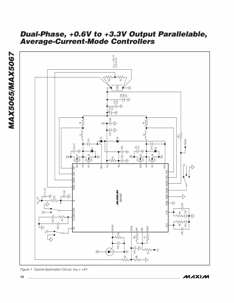
Figure 1. Typical Application Circuit, VIN = +5V
MA
X5
06
5/M
AX
50
67
Dual-Phase, +0.6V to +3.3V Output Parallelable,Average-Current-Mode Controllers
______________________________________________________________________________________ 15
MAX
5067
Q4Q3
C39
C40
R3
D2
Q2
D1
V IN
C8–
C11
Q1
V IN
V CC
D4D3
C41
C12
C38
C3–C
7
C14,
C15
C16–
C25
C26–
C30,
C37
LOAD
L2R2
L1R1
DH1
LX1
DL1
BST1 V D
D
V CC
DH2
LX2
DL2
BST2
CSP2
CSN2
PGOO
DPH
ASE
SGND
PGND
CLP2
CLP1
R11
PGOO
DV C
C
R6
C35
C36
R5 C33
C34
C42
C1, C
2
R13
V CC
C31
C32
R4
CSP1
CSN1
SENS
E+SE
NSE-
INCL
KIN
PLLC
MP
EN
R fR IN
R12
C43
V IN
EAOU
T
EAN
DIFF
OVPI
N
OVPO
UT
C13
C44
RA RB
RH RL
V CC
R X
V OUT
= +
1.8V
AT
52A
V IN
= +8
V TO
+28
V
NOTE
: SEE
TABL
E 1
FOR
COM
PONE
NT V
ALUE
S.
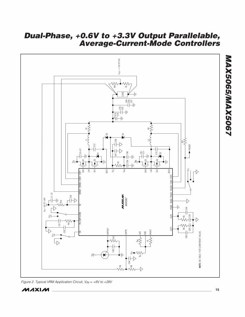
Figure 2. Typical VRM Application Circuit, VIN = +8V to +28V
MA
X5
06
5/M
AX
50
67
Dual-Phase, +0.6V to +3.3V Output Parallelable,Average-Current-Mode Controllers
16 ______________________________________________________________________________________
CLKIN
PLLCMP
PGND
PHASE
DL2
LX2
DH2
DL1
LX1
DH1
VCC
EAOUT
EAN
DIFF
EN
CSP2
CSN2
CSP1
CSN1
MAX5065
3
R1
C39
VIN = +12V
C1,C2
21
15
IN
C25
C26
R4
R7
R8
R6C29
C30
R5C27
C28
SGND
CLP2
CLP1 Q2
Q1
D2
Q2D1
VIN
Q1
VIN
D4
D3
C32
C12
C31
C3–C7
L2 R3
L1 R2
C13
C8–C11 C14,C15
C16–C24,C33
LOAD
+1.8V AT 60AVOUT
SENSE-
SENSE+
17
18
19
16
20
25
24
23
26
9
8
14
13
1
2
BST1
VCC
28
4
10
11
12
7
5
6
22
BST2
RH
RL
VCC
RX
C34
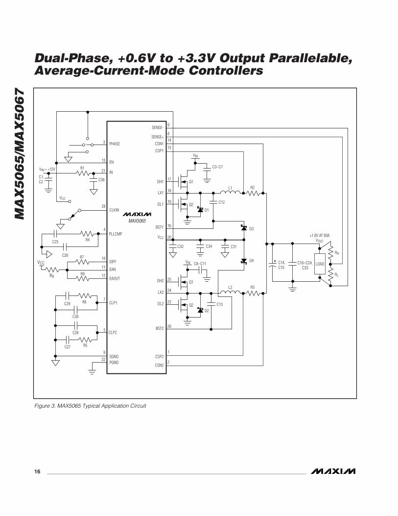
Figure 3. MAX5065 Typical Application Circuit
MA
X5
06
5/M
AX
50
67
Dual-Phase, +0.6V to +3.3V Output Parallelable,Average-Current-Mode Controllers
______________________________________________________________________________________ 17
where, QG1, QG2, QG3, and QG4 are the total gatecharge of the low-side and high-side externalMOSFETs, IQ is 4mA (typ), and fSW is the switching fre-quency of each individual phase.
For applications utilizing a +5V input voltage, disablethe VCC regulator by connecting IN and VCC together.
Undervoltage Lockout (UVLO)/Soft-StartThe MAX5065/MAX5067 include an undervoltage lock-out with hysteresis and a power-on reset circuit for con-verter turn-on and monotonic rise of the output voltage.The UVLO threshold is internally set between +4.0Vand +4.5V with a 200mV hysteresis. Hysteresis atUVLO eliminates “chattering” during startup.
Most of the internal circuitry, including the oscillator,turns on when the input voltage reaches +4V. TheMAX5065/MAX5067 draw up to 4mA of current beforethe input voltage reaches the UVLO threshold.
The compensation network at the current-error ampli-fiers (CLP1 and CLP2) provides an inherent soft-start ofthe output voltage. It includes a parallel combination ofcapacitors (C34, C36) and resistors (R5, R6) in serieswith other capacitors (C33, C35) (see Figures 1 and 2).The voltage at CLP_ limits the maximum current avail-able to charge output capacitors. The capacitor onCLP_ in conjunction with the finite output-drive currentof the current-error amplifier yields a finite rise time forthe output current and thus the output voltage.
Internal OscillatorThe internal oscillator generates the 180° out-of-phaseclock signals required by the pulse-width modulation(PWM) circuits. The oscillator also generates the 2VP-Pvoltage ramp signals necessary for the PWM compara-tors. Connect CLKIN to SGND to set the internal oscillatorfrequency to 250kHz or connect CLKIN to VCC to set theinternal oscillator to 500kHz.
CLKIN is a CMOS logic clock input for the phase-locked loop (PLL). When driven externally, the internaloscillator locks to the signal at CLKIN. A rising edge atCLKIN starts the ON cycle of the PWM. Ensure that theexternal clock pulse width is at least 200ns. CLKOUTprovides a phase-shifted output with respect to the ris-ing edge of the signal at CLKIN. PHASE sets theamount of phase shift at CLKOUT. Connect PHASE toVCC for 120° of phase shift, leave PHASE unconnectedfor 90° of phase shift, or connect PHASE to SGND for60° of phase shift with respect to CLKIN.
The MAX5065/MAX5067 require compensation on PLLCMP even when operating from the internal oscillator.The device requires an active PLL to generate the properclock signal required for PWM operation.
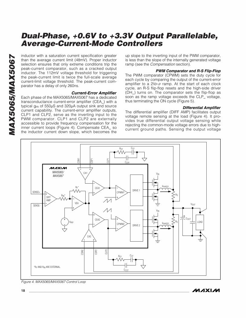
Control LoopThe MAX5065/MAX5067 use an average-current-modecontrol scheme to regulate the output voltage (Figure4). The main control loop consists of an inner currentloop and an outer voltage loop. The inner loop controlsthe output currents (IPHASE1 and IPHASE2) while theouter loop controls the output voltage. The inner currentloop absorbs the inductor pole reducing the order ofthe outer voltage loop to that of a singlepole system.
The current loop consists of a current-sense resistor(RS), a current-sense amplifier (CA_), a current-erroramplifier (CEA_), an oscillator providing the carrierramp, and a PWM comparator (CPWM_). The precisionCA_ amplifies the sense voltage across RS by a factorof 18. The inverting input to the CEA_ senses the CA_output. The CEA_ output is the difference between thevoltage-error amplifier output (EAOUT) and the gained-up voltage from the CA_. The RC compensation net-work connected to CLP1 and CLP2 provides externalfrequency compensation for the respective CEA_. Thestart of every clock cycle enables the high-side driversand initiates a PWM ON cycle. Comparator CPWM_compares the output voltage from the CEA_ with a 0 to+2V ramp from the oscillator. The PWM ON cycle termi-nates when the ramp voltage exceeds the error voltage.
The outer voltage control loop consists of the differen-tial amplifier (DIFF AMP), reference voltage, and VEA.The unity-gain differential amplifier provides true differ-ential remote sensing of the output voltage. The differ-ential amplifier output connects to the inverting input(EAN) of the VEA. The noninverting input of the VEA isinternally connected to an internal precision referencevoltage. The MAX5067 reference voltage is set to +0.8Vand the MAX5065 reference is set to +0.6V. The VEAcontrols the two inner current loops (Figure 4). Use aresistive feedback network to set the VEA gain asrequired by the adaptive voltage-positioning circuit(see the Adaptive Voltage Positioning section).
Current-Sense AmplifierThe differential current-sense amplifier (CA_) provides aDC gain of 18. The maximum input offset voltage of thecurrent-sense amplifier is 1mV and the common-modevoltage range is -0.3V to +3.6V. The current-sense ampli-fier senses the voltage across a current-sense resistor.
Peak-Current ComparatorThe peak-current comparator provides a path for fastcycle-by-cycle current limit during extreme fault condi-tions such as an output inductor malfunction (Figure 5).Note that the average current-limit threshold of 48mVstill limits the output current during short-circuit condi-tions. To prevent inductor saturation, select an output
MA
X5
06
5/M
AX
50
67
Dual-Phase, +0.6V to +3.3V Output Parallelable,Average-Current-Mode Controllers
18 ______________________________________________________________________________________
inductor with a saturation current specification greaterthan the average current limit (48mV). Proper inductorselection ensures that only extreme conditions trip thepeak-current comparator, such as a cracked outputinductor. The 112mV voltage threshold for triggeringthe peak-current limit is twice the full-scale averagecurrent-limit voltage threshold. The peak-current com-parator has a delay of only 260ns.
Current-Error AmplifierEach phase of the MAX5065/MAX5067 has a dedicatedtransconductance current-error amplifier (CEA_) with atypical gm of 550µS and 320µA output sink and sourcecurrent capability. The current-error amplifier outputs,CLP1 and CLP2, serve as the inverting input to thePWM comparator. CLP1 and CLP2 are externallyaccessible to provide frequency compensation for theinner current loops (Figure 4). Compensate CEA_ sothe inductor current down slope, which becomes the
up slope to the inverting input of the PWM comparator,is less than the slope of the internally generated voltageramp (see the Compensation section).
PWM Comparator and R-S Flip-FlopThe PWM comparator (CPWM) sets the duty cycle foreach cycle by comparing the output of the current-erroramplifier to a 2VP-P ramp. At the start of each clockcycle, an R-S flip-flop resets and the high-side driver(DH_) turns on. The comparator sets the flip-flop assoon as the ramp voltage exceeds the CLP_ voltage,thus terminating the ON cycle (Figure 5).
Differential AmplifierThe differential amplifier (DIFF AMP) facilitates outputvoltage remote sensing at the load (Figure 4). It pro-vides true differential output voltage sensing whilerejecting the common-mode voltage errors due to high-current ground paths. Sensing the output voltage
DRIVE 2
DRIVE 1CPWM1
CPWM2
CEA1
CEA2
VEA
DIFFAMP
CA1
CA2
VREF
CLP2
CSP2
CSN2
CLP1
CSN1
CSP1
SENSE+
SENSE-
VIN
VIN
LOADCOUT
VOUT
RIN*
RF*
RS
RS
IPHASE1
IPHASE2
RCF
CCFF
CCF
RCF
CCCF
CCF
*RF AND RIN ARE EXTERNAL.
MAX5065/MAX5067
Figure 4. MAX5065/MAX5067 Control Loop

MA
X5
06
5/M
AX
50
67
Dual-Phase, +0.6V to +3.3V Output Parallelable,Average-Current-Mode Controllers
______________________________________________________________________________________ 19
directly at the load provides accurate load voltagesensing in high-current environments. The VEA pro-vides the difference between the differential amplifieroutput (DIFF) and the desired output voltage. The dif-ferential amplifier has a bandwidth of 3MHz. The differ-ence between SENSE+ and SENSE- regulates to +0.6Vfor the MAX5065 and regulates to +0.8V for theMAX5067. Connect SENSE+ to the center of the resis-tive-divider from the output to SENSE-.
Voltage-Error Amplifier The VEA sets the gain of the voltage control loop anddetermines the error between the differential amplifieroutput and the internal reference voltage (VREF).
The VEA output clamps to +0.9V relative to VCM(+0.6V), thus limiting the average maximum currentfrom individual phases. The maximum average current-limit threshold for each phase is equal to the maximumclamp voltage of the VEA divided by the gain (18) ofthe current-sense amplifier. This results in accurate set-tings for the average maximum current for each phase.Set the VEA gain using RF and RIN for the amount ofoutput voltage positioning required within the rated cur-rent range as discussed in the Adaptive VoltagePositioning section (Figure 4).
where RH and RL are the feedback resistor network
(Figures 1, 2). VREF = 0.6V (MAX5065) or 0.8V(MAX5067).
Some applications require VOUT equal to VOUT(NOM) atno load. To ensure that the output voltage does notexceed the nominal output voltage (VOUT(NOM)), add aresistor RX from VCC to EAN.
Use the following equations to calculate the value of RX.
For MAX5065:
For MAX5067:
Adaptive Voltage PositioningPowering new-generation processors requires newtechniques to reduce cost, size, and power dissipation.Voltage positioning reduces the total number of outputcapacitors to meet a given transient response require-ment. Setting the no-load output voltage slightly higherthan the output voltage during nominally loaded condi-tions allows a larger downward voltage excursion whenthe output current suddenly increases. Regulating at alower output voltage under a heavy load allows a largerupward-voltage excursion when the output current sud-denly decreases. A larger allowed, voltage-step excur-sion reduces the required number of output capacitors
R VR
VX CCF= − ×[ . ]
.1 4
0 8
R VR
VX CCF= − ×[ . ]
.1 2
0 6
VR
R
R R
RVOUT NL
IN
F
H L
LREF( ) = +
×
+
×1
2 x fs (V/s)
RAMP
CLK
CSP_
CSN_
GMIN
SHDN
CLP_
DRV_VCC
BST_
DH_
LX_
DL_
PGND
AV = 18
PWMCOMPARATOR
PEAK-CURRENTCOMPARATOR
112mV
S
R
Q
Q
Gm =500µS
Figure 5. Phase Circuit (Phase 1/Phase 2)
(3)
(4)
(5)
MA
X5
06
5/M
AX
50
67
Dual-Phase, +0.6V to +3.3V Output Parallelable,Average-Current-Mode Controllers
20 ______________________________________________________________________________________
or allows for the use of higher ESR capacitors.
Voltage positioning may require the output to regulateaway from a center value. Define the center value as thevoltage where the output drops (∆VOUT/2) at one half themaximum output current (Figure 6).
Set the voltage-positioning window (∆VOUT) using theresistive feedback of the VEA. Use the following equa-tions to calculate the voltage-positioning window for theMAX5065/MAX5067:
where RIN and RF are the input and feedback resistors ofthe VEA, GC is the current-loop transconductance, andRS is the current-sense resistor.
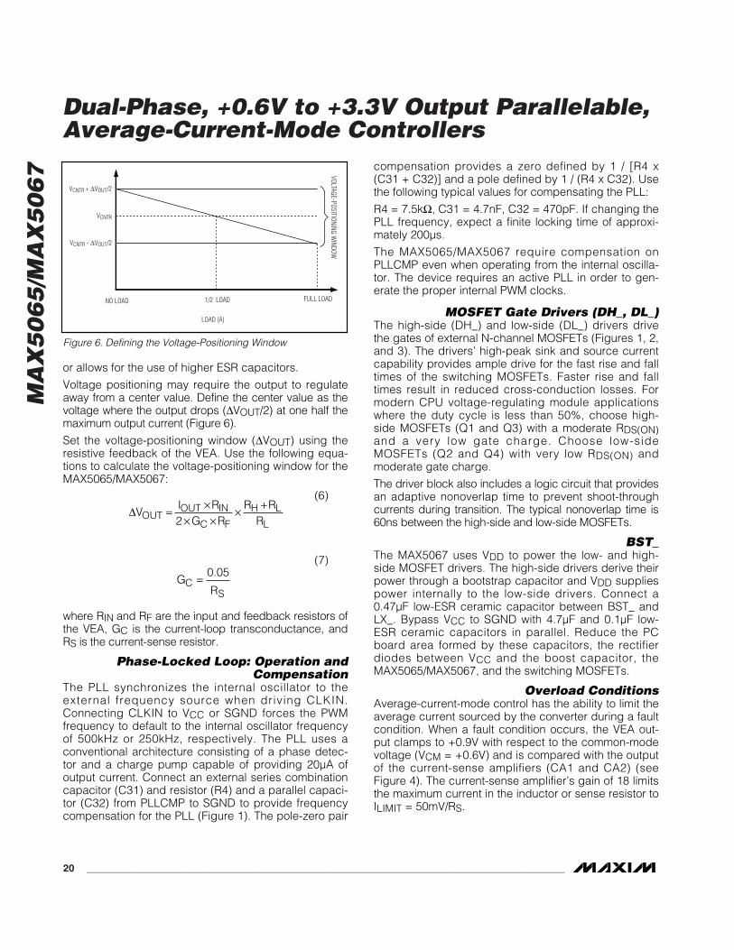
Phase-Locked Loop: Operation andCompensation
The PLL synchronizes the internal oscillator to theexternal frequency source when driving CLKIN.Connecting CLKIN to VCC or SGND forces the PWMfrequency to default to the internal oscillator frequencyof 500kHz or 250kHz, respectively. The PLL uses aconventional architecture consisting of a phase detec-tor and a charge pump capable of providing 20µA ofoutput current. Connect an external series combinationcapacitor (C31) and resistor (R4) and a parallel capaci-tor (C32) from PLLCMP to SGND to provide frequencycompensation for the PLL (Figure 1). The pole-zero pair
compensation provides a zero defined by 1 / [R4 x(C31 + C32)] and a pole defined by 1 / (R4 x C32). Usethe following typical values for compensating the PLL:
R4 = 7.5kΩ, C31 = 4.7nF, C32 = 470pF. If changing thePLL frequency, expect a finite locking time of approxi-mately 200µs.
The MAX5065/MAX5067 require compensation on PLLCMP even when operating from the internal oscilla-tor. The device requires an active PLL in order to gen-erate the proper internal PWM clocks.
MOSFET Gate Drivers (DH_, DL_)The high-side (DH_) and low-side (DL_) drivers drivethe gates of external N-channel MOSFETs (Figures 1, 2,and 3). The drivers’ high-peak sink and source currentcapability provides ample drive for the fast rise and falltimes of the switching MOSFETs. Faster rise and falltimes result in reduced cross-conduction losses. Formodern CPU voltage-regulating module applicationswhere the duty cycle is less than 50%, choose high-side MOSFETs (Q1 and Q3) with a moderate RDS(ON)and a very low gate charge. Choose low-sideMOSFETs (Q2 and Q4) with very low RDS(ON) andmoderate gate charge.
The driver block also includes a logic circuit that providesan adaptive nonoverlap time to prevent shoot-throughcurrents during transition. The typical nonoverlap time is60ns between the high-side and low-side MOSFETs.
BST_The MAX5067 uses VDD to power the low- and high-side MOSFET drivers. The high-side drivers derive theirpower through a bootstrap capacitor and VDD suppliespower internally to the low-side drivers. Connect a0.47µF low-ESR ceramic capacitor between BST_ andLX_. Bypass VCC to SGND with 4.7µF and 0.1µF low-ESR ceramic capacitors in parallel. Reduce the PCboard area formed by these capacitors, the rectifierdiodes between VCC and the boost capacitor, theMAX5065/MAX5067, and the switching MOSFETs.
Overload ConditionsAverage-current-mode control has the ability to limit theaverage current sourced by the converter during a faultcondition. When a fault condition occurs, the VEA out-put clamps to +0.9V with respect to the common-modevoltage (VCM = +0.6V) and is compared with the outputof the current-sense amplifiers (CA1 and CA2) (seeFigure 4). The current-sense amplifier’s gain of 18 limitsthe maximum current in the inductor or sense resistor toILIMIT = 50mV/RS.
GR
CS
= 0 05.
∆VI R
G RR R
ROUTOUT IN
C F
H L
L= ×
× ×× +
2
(6)
(7)
LOAD (A)
VCNTR
NO LOAD 1/2 LOAD FULL LOAD
VOLTAGE-POSITIONING WINDOW
VCNTR + ∆VOUT/2
VCNTR - ∆VOUT/2
Figure 6. Defining the Voltage-Positioning Window

MA
X5
06
5/M
AX
50
67
Dual-Phase, +0.6V to +3.3V Output Parallelable,Average-Current-Mode Controllers
______________________________________________________________________________________ 21
ProtectionThe MAX5067 includes output overvoltage protection(OVP), undervoltage protection (UVP), phase failure,and overload protection to prevent damage to the pow-ered electronic circuits.
Overvoltage Protection (MAX5067)The OVP comparator compares the OVPIN input to theovervoltage threshold (Figure 7). The overvoltagethreshold is typically +0.8V. A detected overvoltageevent latches the comparator output forcing the powerstage into the OVP state. In the OVP state, the high-side MOSFETs turn off and the low-side MOSFETs latchon. Use the OVPOUT high-current output driver to turnon an external crowbar SCR. When the crowbar SCRturns on, a fuse must blow or the source current for theMAX5067 regulator must be limited to prevent furtherdamage to the external circuitry. Connect the SCRclose to the input source and after the fuse. Use anSCR large enough to handle the peak I2t energy due tothe input and output capacitors discharging and thecurrent sourced by the power-source output. ConnectDIFF to OVPIN for differential output sensing and over-voltage protection. Add an RC delay to reduce the sen-sitivity of the overvoltage circuit and avoid nuisancetripping of the converter (Figures 1, 2). Connect a resis-tor-divider from the load to SGND to set the OVP outputvoltage.
Power-Good Generator (MAX5067)The PGOOD output is high if all of the following condi-tions are met (Figure 8):
1) The output is within 90% to 108% of the pro-grammed output voltage.
2) Both phases are providing current.
3) EN is high.
A window comparator compares the differential amplifieroutput (DIFF) against 1.08 times the set output voltagefor overvoltage and 0.90 times the set output voltage forundervoltage monitoring. The phase-failure comparatordetects a phase failure by comparing the current-error-amplifier output (CLP_) with a 2.0V reference.
Use a 10kΩ pullup resistor from PGOOD to a voltagesource less than or equal to VCC. An output voltageoutside the comparator window or a phase-failure con-dition forces the open-drain output low. The open-drainMOSFET sinks 4mA of current while maintaining lessthan 0.2V at the PGOOD output.
VRR
VOVPA
B= +
×1 0 8.
MAX5067
RF
RIN
OVPIN
DIFF
EAN
EAOUT
RB
RAVOUT
Figure 7. OVP Input Delay
+2.0V
PHASE-FAILURE DETECTIONCLP2
CLP1
VREF
DIFF
PGOOD8% OF VREF
10% OF VREF
Figure 8. Power-Good Generator (MAX5067)
(8)

MA
X5
06
5/M
AX
50
67
Dual-Phase, +0.6V to +3.3V Output Parallelable,Average-Current-Mode Controllers
22 ______________________________________________________________________________________
CLKIN
CLKOUTSGNDPGND
IN
PHASE
DL2
LX2
DH2
DL1
LX1
DH1
VCC
VIN
EAOUT
EANDIFF
SENSE-
SENSE+
CSP2
CSN2
CSP1CSN1
VCC
VIN
VIN
CLKOUTSGNDPGND
IN
PHASE
DL2
LX2
DH2
DL1
LX1
DH1
EAOUT
EAN
CLKIN
CSP2
CSN2
CSP1CSN1
DIFF
VCC
VIN
VIN
CLKOUTSGNDPGND
IN
PHASE
DL2
LX2
DH2
DL1
LX1
DH1
EAOUT
EAN
CLKIN
CSP2
CSN2
CSP1CSN1
DIFF
VCC
VIN
VIN
TO OTHER MAX5065/MAX5067s
MAX5065/MAX5067
MAX5065/MAX5067
MAX5065/MAX5067
LOAD VOUT = +0.6V (MAX5065)VOUT = +0.8V (MAX5067)
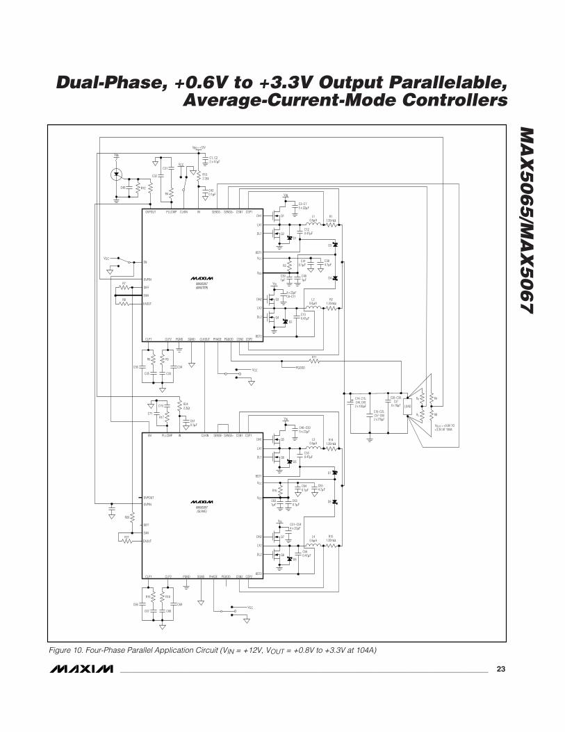
Figure 9. Parallel Configuration of Multiple MAX5065/MAX5067s
MA
X5
06
5/M
AX
50
67
Dual-Phase, +0.6V to +3.3V Output Parallelable,Average-Current-Mode Controllers
______________________________________________________________________________________ 23
MAX5067(MASTER)
Q4
Q3
D2
Q2D1
VIN
4 x 22µFC8–C11
Q1
VIN
VIN = +12V
VCC
D4
D3
C410.1µF
C120.47µF
C384.7µF
C3–C75 x 22µF
L20.6µH
R21.35mΩ
L10.6µH
R11.35mΩ
DH1
LX1
DL1
BST1
VCC
VDD
DH2
LX2
DL2
BST2CSP2CSN2PGOODPHASECLKOUTSGNDPGNDCLP2CLP1
R11
PGOODVCC
R6
C35
C36
R5
C33
C34
C420.1µF
C1, C22 x 47µF
R132.2Ω
C31
C32
R4
CSP1CSN1SENSE+SENSE-INCLKINPLLCMPOVPOUT
R8
R7
EAOUT
EAN
DIFF
OVPIN
EN
C130.47µF
C14, C15,C44, C452 x 100µF
C16–C25,C57–C602 x 270µF
C26–C30,C37
6 x 10µF LOAD
VOUT = +0.8V TO+3.3V AT 104A
VCC
MAX5067(SLAVE)
Q8
Q7
D6
Q6D5
VINC51–C544 x 22µF
Q5
VIN
D8
D7
C640.1µF
C550.47µF
C654.7µF
C46–C505 x 22µF
L40.6µH
R151.35mΩ
L30.6µH
R141.35mΩ
DH1
LX1
DL1
BST1
VCC
VDD
DH2
LX2
DL2
BST2CSP2CSN2PHASE PGOODSGNDPGNDCLP2CLP1
VCC
R19
C67
C66
R18
C68
C69
C610.1µF
R242.2Ω
C70
C71R17
CSP1CSN1SENSE+SENSE-CLKININPLLCMPEN
R21
R20
EAOUT
EAN
DIFF
OVPIN
OVPOUT
C560.47µF
R12C43
VIN
C391µF
C401µF
RH
RL
RA
RB
C621µF
C630.1µF
R16
R3
Figure 10. Four-Phase Parallel Application Circuit (VIN = +12V, VOUT = +0.8V to +3.3V at 104A)
MA
X5
06
5/M
AX
50
67
Dual-Phase, +0.6V to +3.3V Output Parallelable,Average-Current-Mode Controllers
24 ______________________________________________________________________________________
Phase-Failure Detector (MAX5067)Output current contributions from the two phases arewithin ±10% of each other. Proper current sharingreduces the necessity to overcompensate the externalcomponents. However, an undetected failure of onephase driver causes the other phase driver to run con-tinuously as it tries to provide the entire current require-ment to the load. Eventually, the stressed operationalphase driver fails.
During normal operating conditions, the voltage levelon CLP_ is within the peak-to-peak voltage levels of thePWM ramp. If one of the phases fails, the control loopraises the CLP_ voltage above its operating range. Todetermine a phase failure, the phase-failure detectioncircuit (Figure 8) monitors the output of the currentamplifiers (CLP1 and CLP2) and compares them to a2.0V reference. If the voltage levels on CLP1 or CLP2are above the reference level for more than 1250 clockcycles, the phase failure circuit forces PGOOD low.
Parallel OperationFor applications requiring large output current, parallelup to three MAX5065/MAX5067s (six phases) to triplethe available output current (see Figures 9 and 10). Theparalleled converters operate at the same switching fre-quency but different phases keep the capacitor rippleRMS currents to a minimum. Three parallel MAX5065/MAX5067 converters deliver up to 180A of output cur-rent. To set the phase shift of the on-board PLL, leavePHASE unconnected for 90° of phase shift (2 paralleledconverters), or connect PHASE to SGND for 60° of phaseshift (3 converters in parallel). Designate one converteras master and the remaining converters as slaves.Connect the master and slave controllers in a daisy-chain configuration as shown in Figure 9. Connect CLK-OUT from the master controller to CLKIN of the firstslaved controller, and CLKOUT from the first slaved con-troller to CLKIN of the second slaved controller. Choosethe appropriate phase shift for minimum ripple currentsat the input and output capacitors. The master controllersenses the output differential voltage through SENSE+and SENSE- and generates the DIFF voltage. Disable thevoltage sensing of the slaved controllers by leaving DIFFunconnected (floating). Figure 10 shows a detailed typi-cal parallel application circuit using two MAX5067s. Thiscircuit provides four phases at an input voltage of +12Vand an output voltage range of +0.6V to +3.3V(MAX5065) and +0.8V to +3.3V (MAX5067) at 104A.
Applications InformationEach MAX5065/MAX5067 circuit drives two 180° out-of-phase channels. Parallel two or three MAX5065/MAX5067 circuits to achieve four- or six-phase opera-
tion, respectively. Figure 1 shows the typical applicationcircuit for a two-phase operation. The design criteria fora two-phase converter includes frequency selection,inductor value, input/output capacitance, switchingMOSFETs, sense resistors, and the compensation net-work. Follow the same procedure for the four- and six-phase converter design, except for the input and outputcapacitance. The input and output capacitance require-ments vary depending on the operating duty cycle.
The examples discussed in this data sheet pertain to atypical application with the following specifications:
VIN = +12V
VOUT = +1.8V
IOUT(MAX) = 52A
fSW = 250kHz
Peak-to-Peak Inductor Current (∆IL) = 10A
Table 1 shows a list of recommended external compo-nents (Figure 1) and Table 2 provides component sup-plier information.
Number of PhasesSelecting the number of phases for a voltage regulatordepends mainly on the ratio of input-to-output voltage(operating duty cycle). Optimum output-ripple cancella-tion depends on the right combination of operating dutycycle and the number of phases. Use the followingequation as a starting point to choose the number ofphases:
NPH ≈ K/D (9)
where K = 1, 2, or 3 and the duty cycle is D = VOUT/VIN.
Choose K to make NPH an integer number. For exam-ple, converting VIN = +12V to VOUT = +1.8V yields better ripple cancellation in the six-phase converterthan in the four-phase converter. Ensure that the outputload justifies the greater number of components formultiphase conversion. Generally limiting the maximumoutput current to 25A per phase yields the most cost-effective solution. The maximum ripple cancellationoccurs when NPH = K/D.
Single-phase conversion requires greater size and powerdissipation for external components such as the switch-ing MOSFETs and the inductor. Multiphase conversioneliminates the heatsink by distributing the power dissipa-tion in the external components. The multiple phasesoperating at given phase shifts effectively increase theswitching frequency seen by the input/output capacitors,thereby reducing the input/output capacitance require-ment for the same ripple performance. The lower induc-tance value improves the large-signal response of theconverter during a transient load at the output. Consider
MA
X5
06
5/M
AX
50
67
Dual-Phase, +0.6V to +3.3V Output Parallelable,Average-Current-Mode Controllers
______________________________________________________________________________________ 25
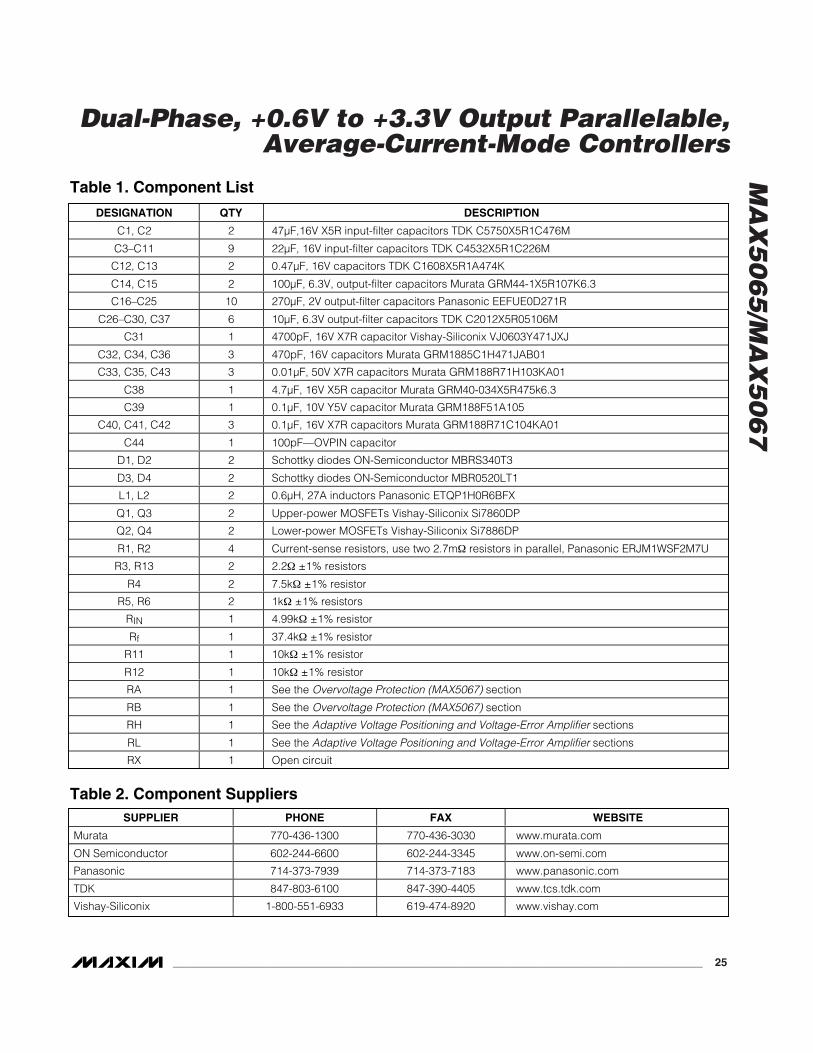
Table 1. Component List
DESIGNATION QTY DESCRIPTION
C1, C2 2 47µF,16V X5R input-filter capacitors TDK C5750X5R1C476M
C3–C11 9 22µF, 16V input-filter capacitors TDK C4532X5R1C226M
C12, C13 2 0.47µF, 16V capacitors TDK C1608X5R1A474K
C14, C15 2 100µF, 6.3V, output-filter capacitors Murata GRM44-1X5R107K6.3
C16–C25 10 270µF, 2V output-filter capacitors Panasonic EEFUE0D271R
C26–C30, C37 6 10µF, 6.3V output-filter capacitors TDK C2012X5R05106M
C31 1 4700pF, 16V X7R capacitor Vishay-Siliconix VJ0603Y471JXJ
C32, C34, C36 3 470pF, 16V capacitors Murata GRM1885C1H471JAB01
C33, C35, C43 3 0.01µF, 50V X7R capacitors Murata GRM188R71H103KA01
C38 1 4.7µF, 16V X5R capacitor Murata GRM40-034X5R475k6.3
C39 1 0.1µF, 10V Y5V capacitor Murata GRM188F51A105
C40, C41, C42 3 0.1µF, 16V X7R capacitors Murata GRM188R71C104KA01
C44 1 100pF—OVPIN capacitor
D1, D2 2 Schottky diodes ON-Semiconductor MBRS340T3
D3, D4 2 Schottky diodes ON-Semiconductor MBR0520LT1
L1, L2 2 0.6µH, 27A inductors Panasonic ETQP1H0R6BFX
Q1, Q3 2 Upper-power MOSFETs Vishay-Siliconix Si7860DP
Q2, Q4 2 Lower-power MOSFETs Vishay-Siliconix Si7886DP
R1, R2 4 Current-sense resistors, use two 2.7mΩ resistors in parallel, Panasonic ERJM1WSF2M7U
R3, R13 2 2.2Ω ±1% resistors
R4 2 7.5kΩ ±1% resistor
R5, R6 2 1kΩ ±1% resistors
RIN 1 4.99kΩ ±1% resistor
Rf 1 37.4kΩ ±1% resistor
R11 1 10kΩ ±1% resistor
R12 1 10kΩ ±1% resistor
RA 1 See the Overvoltage Protection (MAX5067) section
RB 1 See the Overvoltage Protection (MAX5067) section
RH 1 See the Adaptive Voltage Positioning and Voltage-Error Amplifier sections
RL 1 See the Adaptive Voltage Positioning and Voltage-Error Amplifier sections
RX 1 Open circuit
Table 2. Component SuppliersSUPPLIER PHONE FAX WEBSITE
Murata 770-436-1300 770-436-3030 www.murata.com
ON Semiconductor 602-244-6600 602-244-3345 www.on-semi.com
Panasonic 714-373-7939 714-373-7183 www.panasonic.com
TDK 847-803-6100 847-390-4405 www.tcs.tdk.com
Vishay-Siliconix 1-800-551-6933 619-474-8920 www.vishay.com
MA
X5
06
5/M
AX
50
67
Dual-Phase, +0.6V to +3.3V Output Parallelable,Average-Current-Mode Controllers
26 ______________________________________________________________________________________
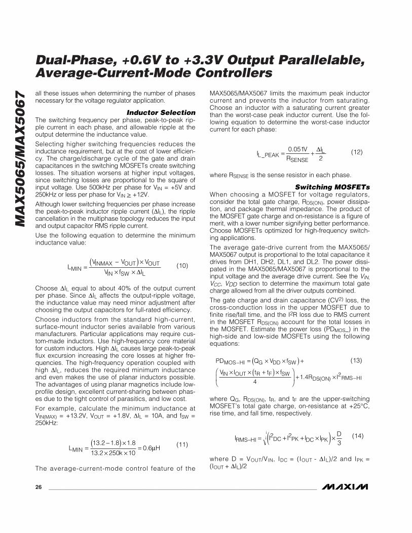
all these issues when determining the number of phasesnecessary for the voltage regulator application.
Inductor SelectionThe switching frequency per phase, peak-to-peak rip-ple current in each phase, and allowable ripple at theoutput determine the inductance value.
Selecting higher switching frequencies reduces theinductance requirement, but at the cost of lower efficien-cy. The charge/discharge cycle of the gate and draincapacitances in the switching MOSFETs create switchinglosses. The situation worsens at higher input voltages,since switching losses are proportional to the square ofinput voltage. Use 500kHz per phase for VIN = +5V and250kHz or less per phase for VIN > +12V.
Although lower switching frequencies per phase increasethe peak-to-peak inductor ripple current (∆IL), the ripplecancellation in the multiphase topology reduces the inputand output capacitor RMS ripple current.
Use the following equation to determine the minimuminductance value:
Choose ∆IL equal to about 40% of the output currentper phase. Since ∆IL affects the output-ripple voltage,the inductance value may need minor adjustment afterchoosing the output capacitors for full-rated efficiency.
Choose inductors from the standard high-current, surface-mount inductor series available from variousmanufacturers. Particular applications may require cus-tom-made inductors. Use high-frequency core materialfor custom inductors. High ∆IL causes large peak-to-peakflux excursion increasing the core losses at higher fre-quencies. The high-frequency operation coupled withhigh ∆IL, reduces the required minimum inductanceand even makes the use of planar inductors possible.The advantages of using planar magnetics include low-profile design, excellent current-sharing between phas-es due to the tight control of parasitics, and low cost.
For example, calculate the minimum inductance atVIN(MAX) = +13.2V, VOUT = +1.8V, ∆IL = 10A, and fSW =250kHz:
The average-current-mode control feature of the
MAX5065/MAX5067 limits the maximum peak inductorcurrent and prevents the inductor from saturating.Choose an inductor with a saturating current greaterthan the worst-case peak inductor current. Use the fol-lowing equation to determine the worst-case inductorcurrent for each phase:
where RSENSE is the sense resistor in each phase.
Switching MOSFETsWhen choosing a MOSFET for voltage regulators,consider the total gate charge, RDS(ON), power dissipa-tion, and package thermal impedance. The product ofthe MOSFET gate charge and on-resistance is a figure ofmerit, with a lower number signifying better performance.Choose MOSFETs optimized for high-frequency switch-ing applications.
The average gate-drive current from the MAX5065/MAX5067 output is proportional to the total capacitance itdrives from DH1, DH2, DL1, and DL2. The power dissi-pated in the MAX5065/MAX5067 is proportional to theinput voltage and the average drive current. See the VIN,VCC, VDD section to determine the maximum total gatecharge allowed from all the driver outputs combined.
The gate charge and drain capacitance (CV2) loss, thecross-conduction loss in the upper MOSFET due tofinite rise/fall time, and the I2R loss due to RMS currentin the MOSFET RDS(ON) account for the total losses inthe MOSFET. Estimate the power loss (PDMOS_) in thehigh-side and low-side MOSFETs using the followingequations:
where QG, RDS(ON), tR, and tF are the upper-switchingMOSFET’s total gate charge, on-resistance at +25°C,rise time, and fall time, respectively.
where D = VOUT/VIN, IDC = (IOUT - ∆IL)/2 and IPK = (IOUT + ∆IL)/2
I I I I ID
RMS HI DC PK DC PK− = + + ×( ) ×2 23
PD Q V f
V I t t fR I
MOS HI G DD SW
IN OUT R F SWDS ON RMS HI
−
−
= × ×( ) +
× × +( ) ×
+ ×
41 4 2. ( )
IV
RI
L PEAKSENSE
L_
.= +0 0512
∆
Lk
HMIN =−( ) ×
× ×= µ
13 2 1 8 1 8
13 2 250 100 6
. . .
..
LV V V
V f IMININMAX OUT OUT
IN SW L=
−( ) ×× × ∆
(10)
(11)
(12)
(13)
(14)

MA
X5
06
5/M
AX
50
67
Dual-Phase, +0.6V to +3.3V Output Parallelable,Average-Current-Mode Controllers
______________________________________________________________________________________ 27
where COSS is the MOSFET drain-to-source capacitance.
For example, from the typical specifications in theApplications Information section with VOUT = +1.8V, thehigh-side and low-side MOSFET RMS currents are 9.9Aand 24.1A, respectively. Ensure that the thermal imped-ance of the MOSFET package keeps the junction tem-perature at least 25°C below the absolute maximumrating. Use the following equation to calculate maxi-mum junction temperature:
TJ = PDMOS x θJ-A + TA
Input CapacitorsThe discontinuous input-current waveform of the buckconverter causes large ripple currents in the inputcapacitor. The switching frequency, peak inductor cur-rent, and the allowable peak-to-peak voltage ripplereflected back to the source dictate the capacitancerequirement. Increasing the number of phases increas-es the effective switching frequency and lowers thepeak-to-average current ratio, yielding a lower inputcapacitance requirement.
The input ripple is comprised of ∆VQ (caused by thecapacitor discharge) and ∆VESR (caused by the ESR ofthe capacitor). Use low-ESR ceramic capacitors withhigh-ripple-current capability at the input. Assume thecontributions from the ESR and capacitor discharge areequal to 30% and 70%, respectively. Calculate theinput capacitance and ESR required for a specified rip-ple using the following equation:
where IOUT is the total output current of the multiphaseconverter and N is the number of phases.
For example, at VOUT = +1.8V, the ESR and inputcapacitance are calculated for the input peak-to-peakripple of 100mV or less yielding an ESR and capaci-tance value of 1mΩ and 200µF.
Output CapacitorsThe worst-case peak-to-peak and capacitor RMS ripplecurrent, the allowable peak-to-peak output ripple volt-age, and the maximum deviation of the output voltageduring step loads determine the capacitance and theESR requirements for the output capacitors.
In multiphase converter design, the ripple currents fromthe individual phases cancel each other and lower theripple current. The degree of ripple cancellationdepends on the operating duty cycle and the number ofphases. Choose the right equation from Table 3 to calcu-late the peak-to-peak output ripple (∆IP-P) for a givenduty cycle of two-, four-, and six-phase converters. Themaximum ripple cancellation occurs when NPH = K / D.
C
IN
D D
V fIN
OUT
Q SW=
× −( )×
1
∆
ESRV
IN
IINESR
OUT L=
( )+
∆∆2
I I I I ID
RMS LO DC PK DC PK− = + + ×( ) ×−( )2 2 1
3
PD Q V f
C V fR I
MOS LO G DD SW
OSS IN SWDS ON RMS LO
−
−
= × ×( ) +
× × ×
+ ×
23
1 42
2. ( )
Table 3. Peak-to-Peak Output RippleCurrent Calculations
NUMBER OFPHASES (N)
DUTYCYCLE (D)
EQUATION FOR ∆IP-P
2 < 50%
2 > 50%
4 0 to 25%
4 25% to 50%
4 > 50%
6 < 17%
∆IV D
L fO
SW= −
×( )1 2
∆IV V D
L fIN O
SW=
−( ) −( )×
2 1
∆IV D
L fO
SW= −
×( )1 4
∆IV D D
D L fO
SW= − −
× × ×( )( )1 2 4 1
2
∆IV D D
D L fO
SW= − −
× ×( )( )2 1 3 4
∆IV D
L fO
SW= −
×( )1 6
(15)
(16)
(17) (18)
(19)

MA
X5
06
5/M
AX
50
67
Dual-Phase, +0.6V to +3.3V Output Parallelable,Average-Current-Mode Controllers
28 ______________________________________________________________________________________
The allowable deviation of the output voltage during thefast transient load dictates the output capacitance andESR. The output capacitors supply the load step untilthe controller responds with a greater duty cycle. Theresponse time (tRESPONSE) depends on the closed-loopbandwidth of the converter. The resistive drop acrossthe capacitor ESR and capacitor discharge causes avoltage drop during a step load. Use a combination ofSP polymer and ceramic capacitors for better transientload and ripple/noise performance.
Keep the maximum output voltage deviation less thanor equal to the adaptive voltage-positioning window(∆VOUT). Assume 50% contribution each from the out-put capacitance discharge and the ESR drop. Use thefollowing equations to calculate the required ESR andcapacitance value:
where ISTEP is the load step and tRESPONSE is theresponse time of the controller. Controller responsetime depends on the control-loop bandwidth.
Current LimitThe average-current-mode control technique of theMAX5065/MAX5067 accurately limits the maximum out-put current per phase. The MAX5065/MAX5067 sensethe voltage across the sense resistor and limit the peakinductor current (IL-PK) accordingly. The ON cycle ter-minates when the current-sense voltage reaches 45mV(min). Use the following equation to calculate maximumcurrent-sense resistor value:
where PDR is the power dissipation in sense resistors.Select 5% lower value of RSENSE to compensate for anyparasitics associated with the PC board. Also, select anon inductive resistor with the appropriate wattage rating.
Reverse Current LimitThe MAX5065/MAX5067 limit the reverse current whenVBUS is higher than the preset output voltage.
Calculate the maximum reverse current based on VCLR,the reverse-current-limit threshold, and the current-senseresistor.
where IREVERSE is the total reverse current into the con-verter.
CompensationThe main control loop consists of an inner current loopand an outer voltage loop. The MAX5065/MAX5067 usean average-current-mode control scheme to regulatethe output voltage (Figure 4). IPHASE1 and IPHASE2 arethe inner average current loops. The VEA output pro-vides the controlling voltage for these current sources.The inner current loop absorbs the inductor pole reduc-ing the order of the outer voltage loop to that of a sin-gle-pole system.
A resistive feedback around the VEA provides the bestpossible response, since there are no capacitors tocharge and discharge during large-signal excursions, RFand RIN determine the VEA gain. Use the following equa-tion to calculate the value for RF:
where GC is the current-loop transconductance and Nis number of phases.
When designing the current-control loop ensure that theinductor downslope (when it becomes an upslope at theCEA output) does not exceed the ramp slope. This is anecessary condition to avoid sub-harmonic oscillationssimilar to those in peak current-mode control with insuffi-cient slope compensation. Use the following equation tocalculate the resistor RCF:
For example, the maximum RCF is 12kΩ for RSENSE =1.35mΩ.
CCF provides a low-frequency pole while RCF provides amidband zero. Place a zero at fZ to obtain a phase bumpat the crossover frequency. Place a high-frequency pole
Rf L
V RCFSW
OUT SENSE≤ × × ×
×2 102
GRC
S= 0 05.
RI R
N G VFOUT IN
C OUT=
×× × ∆
IV
RREVERSECLR
SENSE= ×2
PDRR
SENSE= × −2 5 10 3.
RI
N
SENSEOUT
= 0 045.
CI t
VOUT
STEP RESPONSE
Q=
×∆
ESRV
IOUTESR
STEP= ∆ (20)
(21)
(22)
(23)
(25)
(26)
(27)
(24)
MA
X5
06
5/M
AX
50
67
Dual-Phase, +0.6V to +3.3V Output Parallelable,Average-Current-Mode Controllers
______________________________________________________________________________________ 29
(fP) at least a decade away from the crossover frequencyto achieve maximum phase margin.
Use the following equations to calculate CCF and CCFF:
PC Board LayoutUse the following guidelines to layout the switchingvoltage regulator:
1) Place the VIN and VCC bypass capacitors close tothe MAX5065/MAX5067.
2) Minimize the area and length of the high-currentloops from the input capacitor, upper switchingMOSFET, inductor, and output capacitor back tothe input capacitor negative terminal.
3) Keep short the current loop from the lower-switch-ing MOSFET, inductor, and output capacitor.
4) Place the Schottky diodes close to the lowerMOSFETs and on the same side of the PC board.
5) Keep the SGND and PGND isolated and connectthem at one single point close to the negative termi-nal of the input-filter capacitor.
6) Run the current-sense lines CS+ and CS- veryclose to each other to minimize the loop area.Similarly, run the remote-voltage sense linesSENSE+ and SENSE- close to each other. Do notcross these critical signal lines through power cir-cuitry. Sense the current right at the pads of thecurrent-sense resistors.
7) Avoid long traces between the VCC bypass capaci-tors, driver output of the MAX5065/MAX5067, MOSFET gates and PGND pin. Minimize the loopformed by the VCC bypass capacitors, bootstrapdiode, bootstrap capacitor, MAX5065/MAX5067,and upper MOSFET gate.
8) Place the bank of output capacitors close to the load.
9) Distribute the power components evenly across theboard for proper heat dissipation.
10) Provide enough copper area at and around theswitching MOSFETs, inductor, and sense resistorsto aid in thermal dissipation.
11) Use at least 4oz copper to keep the trace induc-tance and resistance to a minimum. Thin copper PCboards can compromise efficiency since high cur-rents are involved in the application. Also, thickercopper conducts heat more effectively, therebyreducing thermal impedance.
Chip InformationTRANSISTOR COUNT: 5451
PROCESS: BiCMOS
Cf RCFFP CF
=× × ×
12 π
Cf RCFZ CF
=× × ×
12 π
(28)
(29)
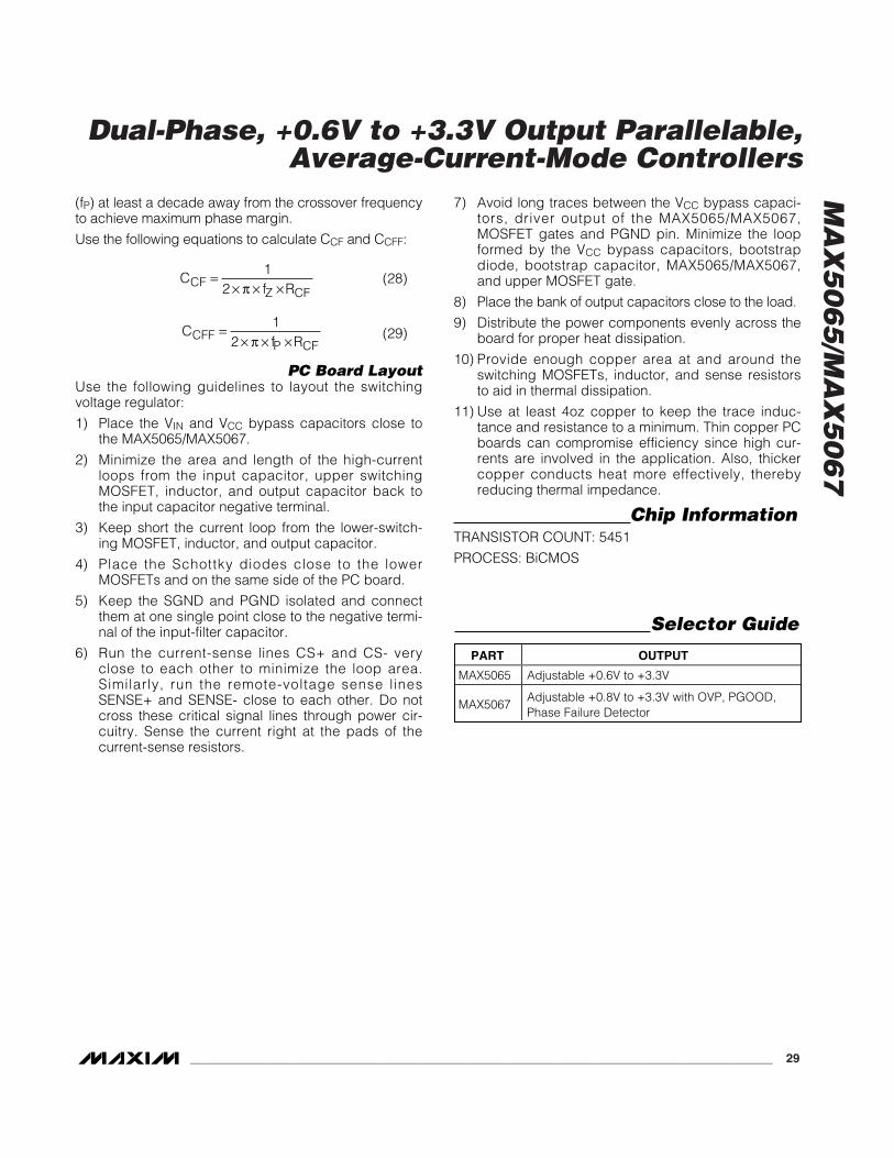
Selector Guide
PART OUTPUT
MAX5065 Adjustable +0.6V to +3.3V
MAX5067Adjustable +0.8V to +3.3V with OVP, PGOOD,Phase Failure Detector
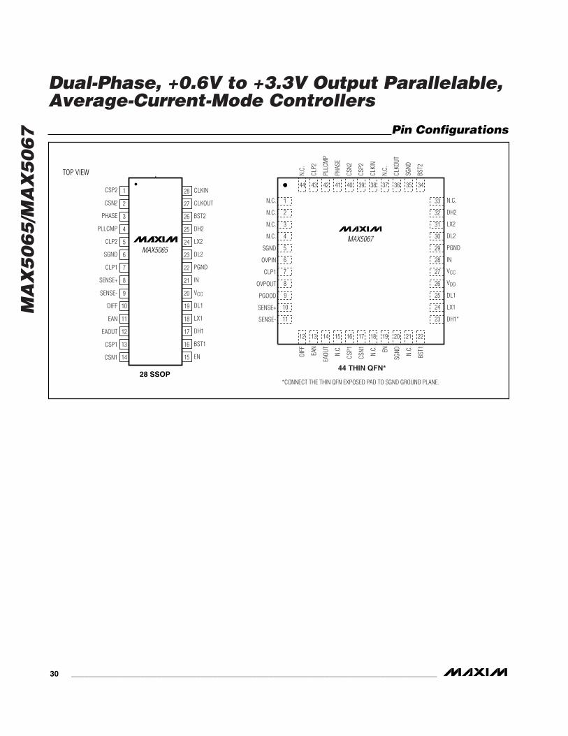
MA
X5
06
5/M
AX
50
67
Dual-Phase, +0.6V to +3.3V Output Parallelable,Average-Current-Mode Controllers
Pin Configurations
28 SSOP
TOP VIEW
MAX5065
1
2
3
CSP2
CSN2
PHASE
4
VCC
5
6
7
CLP2
SGND
CLP1
28
27
26
CLKIN
CLKOUT
BST2
25 DH2
24
23
22
LX2
DL2
PGND
8
9
10
SENSE+
SENSE-
DIFF
11EAN
12
13
14
EAOUT
CSP1
CSN1
21
20
19
IN
DL1
18 LX1
17
16
15
DH1
BST1
EN
PLLCMPN.C.
N.C.
SGND
OVPIN
N.C.
CLP1
OVPOUT
EAN
N.C.
EAOU
TDH1*
PGOOD
VCC
SENSE+
SENSE-
*CONNECT THE THIN QFN EXPOSED PAD TO SGND GROUND PLANE.
BST1
LX1
VDD
DL1
PGND
LX2
DL2
IN
DH2
N.C.
CLP2
BST2
N.C.
DIFF
N.C.1
2
3
4
5
6
7
8
9
10
11
14 15 16 17 18 19 20 21 2212 13
CSP1
CSN1 N.C. EN
SGND N.C.
33
32
31
30
29
28
27
26
25
24
23
44 43 42 41 40 39 38 37 36 35 34
PLLC
MP
CSP2
CLKO
UT
PHAS
E
CSN2
CLKI
N
N.C.
SGND
44 THIN QFN*
MAX5067
30 _____________________________________________________________________________________

MA
X5
06
5/M
AX
50
67
Dual-Phase, +0.6V to +3.3V Output Parallelable,Average-Current-Mode Controllers
______________________________________________________________________________________ 31
SS
OP
.EP
S
PACKAGE OUTLINE, SSOP, 5.3 MM
11
21-0056 CREV.DOCUMENT CONTROL NO.APPROVAL
PROPRIETARY INFORMATION
TITLE:
NOTES:1. D&E DO NOT INCLUDE MOLD FLASH.2. MOLD FLASH OR PROTRUSIONS NOT TO EXCEED .15 MM (.006").3. CONTROLLING DIMENSION: MILLIMETERS.4. MEETS JEDEC MO150.5. LEADS TO BE COPLANAR WITHIN 0.10 MM.
7.90H
L
0∞
0.301
0.025
8∞
0.311
0.037
0∞
7.65
0.63
8∞
0.95
MAX
5.38
MILLIMETERS
B
C
D
E
e
A1
DIM
A
SEE VARIATIONS
0.0256 BSC
0.010
0.004
0.205
0.002
0.015
0.008
0.212
0.008
INCHES
MIN MAX
0.078
0.65 BSC
0.25
0.09
5.20
0.05
0.38
0.20
0.21
MIN
1.73 1.99
MILLIMETERS
6.07
6.07
10.07
8.07
7.07
INCHES
D
D
D
D
D
0.239
0.239
0.397
0.317
0.278
MIN
0.249
0.249
0.407
0.328
0.289
MAX MIN
6.33
6.33
10.33
8.33
7.33
14L
16L
28L
24L
20L
MAX N
A
D
e A1 L
C
HE
N
12
B
0.068
Package Information(The package drawing(s) in this data sheet may not reflect the most current specifications. For the latest package outline information,go to www.maxim-ic.com/packages.
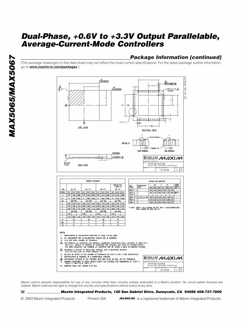
Package Information (continued)(The package drawing(s) in this data sheet may not reflect the most current specifications. For the latest package outline information,go to www.maxim-ic.com/packages.)
32, 4
4, 4
8L Q
FN.E
PS
PROPRIETARY INFORMATION
APPROVAL
TITLE:
DOCUMENT CONTROL NO.
21-0144
PACKAGE OUTLINE32, 44, 48L THIN QFN, 7x7x0.8 mm
1C
REV.
2
e
L
e
L
A1A
A2
E/2
E
D/2
D
DETAIL A
D2/2
D2
b
L
k
E2/2
E2(NE-1) X e
(ND-1) X e
e
CLCL
CL
CL
k
DALLASSEMICONDUCTOR
PROPRIETARY INFORMATION
DOCUMENT CONTROL NO.APPROVAL
TITLE:
CREV.
22
21-0144
PACKAGE OUTLINE32, 44, 48L THIN QFN, 7x7x0.8 mm
DALLASSEMICONDUCTOR
MA
X5
06
5/M
AX
50
67
Dual-Phase, +0.6V to +3.3V Output Parallelable,Average-Current-Mode Controllers
Maxim cannot assume responsibility for use of any circuitry other than circuitry entirely embodied in a Maxim product. No circuit patent licenses areimplied. Maxim reserves the right to change the circuitry and specifications without notice at any time.
32 ____________________Maxim Integrated Products, 120 San Gabriel Drive, Sunnyvale, CA 94086 408-737-7600
© 2003 Maxim Integrated Products Printed USA is a registered trademark of Maxim Integrated Products.