dual-band reflectarrays using … · reflector antenna with an offset feed configuration ... axial...
TRANSCRIPT

DUAL-BAND REFLECTARRAYS USING MICROSTRIP RING
ELEMENTS AND THEIR APPLICATIONS WITH VARIOUS
FEEDING ARRANGEMENTS
A Dissertation
by
CHUL MIN HAN
Submitted to the Office of Graduate Studies of Texas A&M University
in partial fulfillment of the requirements for the degree of
DOCTOR OF PHILOSOPHY
August 2006
Major Subject: Electrical Engineering
DUAL-BAND REFLECTARRAYS USING MICROSTRIP RING
ELEMENTS AND THEIR APPLICATIONS WITH VARIOUS
FEEDING ARRANGEMENTS
A Dissertation
by
CHUL MIN HAN
Submitted to the Office of Graduate Studies of Texas A&M University
in partial fulfillment of the requirements for the degree of
DOCTOR OF PHILOSOPHY
Approved by: Chair of Committee, Kai Chang Committee Members, Robert D. Nevels Chin B. Su Thomas Wilheit Head of Department, Costas N. Georgiades
August 2006
Major Subject: Electrical Engineering

iii
ABSTRACT
Dual-Band Reflectarrays Using Microstrip Ring Elements and Their Applications with
Various Feeding Arrangements. (August 2006)
Chul Min Han, B.S., Korea University
Chair of Advisory Committee: Dr. Kai Chang
In recent years there has been a growing demand for reduced mass, small launch
volume, and, at the same time, high-gain large-aperture antenna systems in modern
space-borne applications. This dissertation introduces new techniques for dual-band
reflectarray antennas to meet these requirements. A series of developments is presented
to show the dual-band capability of the reflectarray.
A novel microstrip ring structure has been developed to achieve circular
polarization (CP). A C/Ka dual-band front-fed reflectarray antenna has been designed to
demonstrate the dual-band circular polarized operation. The proposed ring structure
provides many advantages of compact size, more freedom in the selection of element
spacing, less blockage between circuit layers, and broader CP bandwidth as compared to
the patches.
An X/Ka dual-band offset-fed reflectarray is made of thin membranes, with their
thickness equal to 0.0508 mm in both layers. Several degrading effects of thin substrates
are discussed. To overcome these problems, a new configuration is developed by
inserting empty spaces of the proper thickness below both the X and Ka band
membranes. More than 50 % efficiencies are achieved at both frequency ranges, and the

iv
proposed scheme is expected to be a good candidate to meet the demand for future
inflatable antenna systems.
An X/Ka dual-band microstrip reflectarray with circular polarization has also been
constructed using thin membranes and a Cassegrain offset-fed configuration. It is
believed that this is the first Cassegrain reflectarray ever developed. This antenna has a
0.75-meter-diameter aperture and uses a metallic sub-reflector and angular-rotated
annular ring elements. It achieved a measured 3 dB gain bandwidth of 700 MHz at X-
band and 1.5 GHz at Ka-band, as well as a CP bandwidth (3 dB axial ratio) of more than
700 MHz at X-band and more than 2 GHz at Ka-band. The measured peak efficiencies
are 49.8 % at X-band and 48. 2 % at Ka-band.
In summary, this dissertation presents a series of new research developments to
support the dual-band operation of the reflectarray antenna. The results of this work are
currently being implemented onto a 3-meter reflectarray with inflatable structures at the
Jet Propulsion Laboratory and are planned for other applications such as an 8-meter
inflatable reflectarray in the near future.

v
To my wife Yongsuk, whose encouragement, love, and support have made all of this possible.

vi
ACKNOWLEDGMENTS
Thank you, Lord for the blessings you have given me. Your mercy and love is
with me guiding my life. Thank you for everything you have done.
I would like to express my deepest gratitude to Dr. Kai Chang for his support and
guidance throughout my graduate studies and research at Texas A&M University. I also
appreciate Dr. Robert D. Nevels, Dr. Chin B. Su, Dr. Thomas Wilheit and Dr. Ugur
Cilingiroglu for serving as members on my dissertation committee and for their helpful
comments.
I would like to thank Mr. Ming-yi Li for his technical assistance. I gratefully
acknowledge all my friends and members of the Electromagnetics and Microwave
Laboratory for their technical assistance, incentives and valuable discussions. I would
also like to give special thanks to Dr. John Huang at the Jet Propulsion Laboratory for
his support of my research and helpful comments.
I would like to thank my parents and all my brothers and sisters for their constant
love, encouragement, and support. I also thank my two sons, Seulchan and Gaon, for
their love. Finally, my sincere thanks are given to my lovely wife, Yongsuk, for all her
patience, love, and support during my graduate studies.

vii
TABLE OF CONTENTS
Page
ABSTRACT..................................................................................................................... iii
DEDICATION ...................................................................................................................v
ACKNOWLEDGMENTS.................................................................................................vi
TABLE OF CONTENTS................................................................................................ vii
LIST OF FIGURES...........................................................................................................ix
LIST OF TABLES ..........................................................................................................xiv
CHAPTER
I INTRODUCTION............................................................................................1
II FRONT-FED C/KA DUAL-BAND REFLECTARRAY ANTENNA............7
1. Introduction ................................................................................................7 2. Reflecting antenna array analysis.............................................................10 3. Circularly polarized antenna element design ...........................................18 4. Experiments..............................................................................................22 5. Conclusions ..............................................................................................31
III OFFSET-FED X/KA DUAL-BAND REFLECTARRAY ANTENNA
USING THIN MEMBRANES.......................................................................32
1. Introduction ..............................................................................................32 2. Offset reflecting antenna analysis ............................................................36 3. Element design .........................................................................................41 4. Experiments..............................................................................................46 5. Conclusions ..............................................................................................58

viii
CHAPTER Page
IV CASSEGRAIN OFFSET SUB-REFLECTOR-FED X/KA DUAL-BAND
REFLECTARRAY WITH THIN MEMBRANES ........................................60
1. Introduction ..............................................................................................60 2. Cassegrain sub-reflector design ...............................................................62 3. Feed array design .....................................................................................66 4. Offset reflecting antenna analysis ............................................................76 5. Experiments..............................................................................................79 6. Conclusions ..............................................................................................92
V SUMMARY AND RECOMMENDATIONS................................................94
1. Summary ..................................................................................................94 2. Recommendations for future research......................................................95
REFERENCES.................................................................................................................96
APPENDIX A ................................................................................................................104
APPENDIX B ................................................................................................................108
APPENDIX C ................................................................................................................119
VITA ..............................................................................................................................130

ix
LIST OF FIGURES
FIGURE Page
1. Reflector antenna with an offset feed configuration.................................................1
2. A reflectarray antenna...............................................................................................2
3. Various reflectarray elements: (a) identical patches with different-length delay lines; (b) variable-size dipoles; (c) variable-size patches; (d) variable angular rotations. ...................................................................................................................3
4. A photo of the reflectarray with microstrip rings of variable rotations and a CP feed horn....................................................................................................9
5. Dual-band reflectarray topology.. .............................................................................9
6. Circularly polarized patch element: (a) reference element with 0o phase shift; (b) ψ degree rotated element with 2ψ degree phase shift. .....................................10
7. Center-fed reflectarray block diagram....................................................................13
8. Element location and rotation. ................................................................................14
9. Required rotation angles simulated in Matlab: (a) C-band; (b) Ka-band. ..............17
10. Ring antenna elements: (a) C-band; (b) Ka-band ...................................................19
11. Comparison of cross-polarization suppression in dB at 32 GHz............................19
12. Relative phase variations at a focal point referenced to zero rotation when the ring element is rotated in the counter-clockwise direction .....................20
13. 7 by 7 arrays simulated result at 32 GHz with and without the top layer of 2 by 2 arrays............................................................................................................21
14. Measured CP gains for a C band reflectarray. ........................................................23
15. Measured gain variations versus frequency at C-band for a dual layer..................24
16. Aperture efficiencies versus frequency for a dual layer .........................................24
17. Axial ratios at broadside versus frequency for a dual layer....................................25

x
FIGURE Page
18. Axial ratio variations versus incident angle for a dual layer ..................................26
19. CP radiation patterns at 31.75 GHz ........................................................................27
20. CP gain variations versus frequency.......................................................................28
21. Aperture efficiencies versus frequency...................................................................29
22. Axial ratios at broadside versus frequency .............................................................30
23. Axial ratio variations versus frequency for a dual layer. ........................................30
24. (a) A photo of the half-meter offset-fed reflectarray with microstrip rings of variable rotations (b) close-up view of the reflectarray element ............................35
25. Two-layer reflectarray topology with element dimensions. ...................................35
26. Offset-fed reflectarray block diagram.....................................................................36
27. Required rotation angles simulated in Matlab: (a) X-band; (b) Ka-band ...............40
28. H-wall waveguide approach: (a) Isometric view; (b) Boundary of four side walls and direction of electric field. .................................................................................42
29. Comparison of cross-polarization suppression level in dB at 32 GHz. ..................44
30. Simulation setup with different excitation scheme: (a) horizontal excitation; (b) vertical excitation....................................................................................................44
31. Normalized radiation patterns in the plane perpendicular to the offset plane at 32.2 GHz. ............................................................................................................47
32. Peak sidelobe level variations in the plane perpendicular to the offset plane at Ka-band...............................................................................................................48
33. Axial ratios versus frequency in the plane perpendicular to the offset plane at Ka-band...............................................................................................................48
34. Normalized radiation patterns in the offset plane at 32.2 GHz. .............................50
35. Peak sidelobe level variations in the offset plane at Ka-band. ...............................50
36. Axial ratios versus frequency in the offset plane at Ka-band .................................51

xi
FIGURE Page
37. Measured aperture efficiencies versus frequency at Ka-band. ...............................52
38. Normalized radiation patterns in the plane perpendicular to the offset plane at 8.7 GHz...............................................................................................................53
39. Peak sidelobe level variations in the plane perpendicular to the offset plane at X-band.................................................................................................................54
40. Axial ratios versus frequency in the plane perpendicular to the offset plane at X-band.................................................................................................................54
41. Normalized radiation patterns in the offset plane at 8.7 GHz ................................55
42. Peak sidelobe level variations in the offset plane at X-band. .................................56
43. Axial ratio versus frequency in the offset plane at X-band. ...................................56
44. Measured aperture efficiencies versus frequency at X-band. .................................57
45. The offset Cassegrain geometry and the projected sub-reflector rim shape with photo of fabricated sub-reflector. ...................................................................62
46. Normalized radiation patterns at a distance of r=2.5 oλ versus aperture size. .......67
47. Normalized radiation patterns at a distance of r=9.5 oλ versus aperture size ........68
48. Feed arrays at both X and Ka-bands: (a) schematic of feed arrays; (b) photo of fabricated feed arrays..........................................................................69
49. Measured return loss at X-band. .............................................................................70
50. Normalized CP radiation patterns for X-band feed arrays. ....................................71
51. Axial ratio in dB at boresight for X-band feed arrays. ...........................................71
52. Gain and directivity variations versus frequency for X-band feed arrays. .............72
53. Measured return loss at Ka-band. ...........................................................................74
54. Normalized CP radiation patterns for Ka-band feed arrays....................................75
55. Axial ratio in dB at boresight for Ka-band feed arrays...........................................75

xii
FIGURE Page
56. Gain and directivity variations versus frequency for Ka-band feed arrays. ...........76
57. Modified side view of the dual-reflector system. ...................................................77
58. A photo of the reflectarray incorporated with the sub-reflector and the feed array....................................................................................................80
59. Measurement layout dimensions for X-band reflectarray. .....................................81
60. Measurement layout dimensions for Ka-band reflectarray.....................................81
61. Normalized CP radiation patterns at 8.4 GHz: (a) in the offset-plane for X-band only layer; b) in the offset-plane for both X/Ka-band layer; (c) in the plane of asymmetry for X-band only layer; (d) in the plane of asymmetry for both X/Ka-band layer................................................................................................................82
62. Aperture efficiencies versus frequency at X-band..................................................86
63. Axial ratios versus frequency at X-band.................................................................86
64. Normalized CP radiation patterns at 31.8 GHz: (a) in the offset-plane for Ka-band only layer; (b) in the offset-plane for both X/Ka-band layer; (c) in the plane of asymmetry for Ka-band only layer; (d) in the plane of asymmetry for both X/Ka-band layer................................................................................................................87
65. Aperture efficiencies versus frequency at Ka-band. ...............................................91
66. Axial ratios versus frequency at Ka-band...............................................................91
B1. Normalized radiation patterns (dB) in the plane of asymmetry at Ka-band: (a) 31.1 GHz; (b) 31.5 GHz; (c) 32 GHz; (d) 32.8 GHz (co-pol.); (e) 32.8 GHz (cross-pol.). .....................................................................................108
B2. Normalized radiation patterns (dB) in the plane of symmetry at Ka-band: (a) 31.1 GHz; (b) 31.5 GHz; (c) 32 GHz; (d) 32.8 GHz (co-pol.); (e) 32.8 GHz (cross-pol.).. ....................................................................................111
B3. Normalized radiation patterns (dB) in the plane of aymmetry at X-band: (a) 8.2 GHz; (b) 8.4 GHz; (c) 8.5 GHz (co-pol.);(d) 8.9 GHz; (d) 8.5 GHz (cross-pol.).. ......................................................................................114
B4. Normalized radiation patterns (dB) in the plane of symmetry at X-band: (a) 8.2 GHz; (b) 8.4 GHz; (c) 8.5 GHz; (d) 8.9 GHz............................................117
xiii
FIGURE Page
C1. Normalized radiation patterns (dB) in the asymmetric plane at X-band: (a) 8.2 GHz; (b) 8.3 GHz; (c) 8.5 GHz; (d) 8.6 GHz............................................119
C2. Normalized radiation patterns (dB) in the offset plane at X-band: (a) 8.0 GHz; (b) 8.3 GHz; (c) 8.5 GHz; (d) 8.7 GHz............................................122
C3. Normalized radiation patterns (dB) in the asymmetric plane at Ka-band: (a) 31 GHz; (b) 31.4 GHz; (c) 32 GHz; (d) 32.6 GHz; (e) 33 GHz......................124
C4. Normalized radiation patterns (dB) in the offset plane at Ka-band: (a) 31 GHz; (b) 31.6 GHz; (c) 32 GHz; (d) 32.4 GHz; (e) 33 GHz......................127

xiv
LIST OF TABLES
TABLE Page
1. Performance summary for a center-fed reflectarray. ..............................................31
2. Performance summary for an offset-fed reflectarray using thin membranes .........59
3. Design parameters of a Cassegrain dual-reflector system......................................64
4. Calculated design values of a Cassegrain dual-reflector system ............................65
5. Sub-reflector parameters to be considered in the feed design ................................66
6. Locations of the reflectarray surface (units in mm)................................................79
7. Performance summary of a Cassegrain offset-fed reflectarray ..............................93

1
CHAPTER I*
INTRODUCTION
The conventional high-gain antenna most often used is a reflector antenna [1]. It has
been widely used for decades in radars, telecommunications, direct broadcast, radio
astronomy, and deep-space explorations. The reflector antenna shown in Figure 1 is simple
in geometry and mature in design methodology. It features high-gain characteristic over
wide frequency ranges and can accommodate high levels of power. However, the reflector
antenna has a curved structure leading to manufacturing difficulty. It is heavy and its bulky
size makes it occupy more space than a planar antenna. Without the mechanical movement,
the main beam has only limited scan angle.
Fig. 1. Reflector antenna with an offset feed configuration.
The journal model for this dissertation is IEEE Transactions on Antennas and Propagations.
2
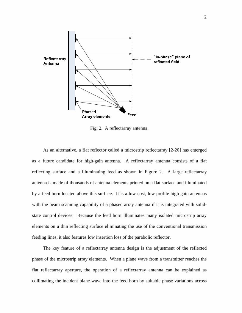
Fig. 2. A reflectarray antenna.
As an alternative, a flat reflector called a microstrip reflectarray [2-20] has emerged
as a future candidate for high-gain antenna. A reflectarray antenna consists of a flat
reflecting surface and a illuminating feed as shown in Figure 2. A large reflectarray
antenna is made of thousands of antenna elements printed on a flat surface and illuminated
by a feed horn located above this surface. It is a low-cost, low profile high gain antennas
with the beam scanning capability of a phased array antenna if it is integrated with solid-
state control devices. Because the feed horn illuminates many isolated microstrip array
elements on a thin reflecting surface eliminating the use of the conventional transmission
feeding lines, it also features low insertion loss of the parabolic reflector.
The key feature of a reflectarray antenna design is the adjustment of the reflected
phase of the microstrip array elements. When a plane wave from a transmitter reaches the
flat reflectarray aperture, the operation of a reflectarray antenna can be explained as
collimating the incident plane wave into the feed horn by suitable phase variations across
3
the surface of the reflectarray.
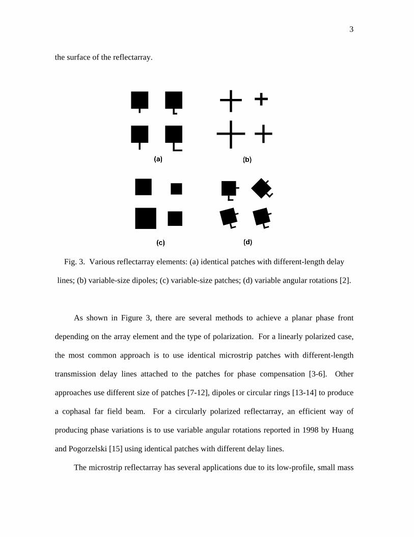
Fig. 3. Various reflectarray elements: (a) identical patches with different-length delay
lines; (b) variable-size dipoles; (c) variable-size patches; (d) variable angular rotations [2].
As shown in Figure 3, there are several methods to achieve a planar phase front
depending on the array element and the type of polarization. For a linearly polarized case,
the most common approach is to use identical microstrip patches with different-length
transmission delay lines attached to the patches for phase compensation [3-6]. Other
approaches use different size of patches [7-12], dipoles or circular rings [13-14] to produce
a cophasal far field beam. For a circularly polarized reflectarray, an efficient way of
producing phase variations is to use variable angular rotations reported in 1998 by Huang
and Pogorzelski [15] using identical patches with different delay lines.
The microstrip reflectarray has several applications due to its low-profile, small mass

4
characteristic [16]. The flat reflectarray can be surface-mounted on a building’s side wall
or rooftop as a Ku-band Direct Broadcast Satellite (DBS) antenna because it takes less
space, or it can be mounted on the rooftop of a large vehicle for satellite reception. The
reflectarray antenna can also be used in space application due to its flat reflecting surface.
For space application, the reflectarray and the solar array panels can be combined into one
large panel saving space efficiently. Another important application of the microstrip
reflectarray is a Ka-band circularly polarized reflectarray for NASA’s future spacecraft
communication antenna application. For large-aperture spacecraft antenna applications, the
reflectarray’s flat surface allows the antenna to be constructed as an inflatable structure
with relative ease in maintaining its surface tolerance in comparison to a curved parabolic
surface.
With all the above characteristics, there is one distinct disadvantage associated with
the reflectarray antenna and it is its inherent narrow bandwidth [17-18] due to different
path lengths or the differential spatial phase delays. It is caused by the path length
differences between the feed to the center elements and the feed to the edge elements. In
other words, the phase change of these path length differences versus the change of
frequency can be a large portion of a wavelength and thus cause performance degradation.
This narrow bandwidth generally cannot exceed beyond ten percent depending on its
element design, aperture size, focal length, etc.
While narrow in bandwidth, microstrip reflectarray antennas are well-suited for dual-
frequency operation in a stacked configuration [19-20]. This dessertation introduces dual-
band reflectarray antennas for future spacecraft antenna applications. A series of
developments are presented to show the dual-band capability of the reflectarray with

5
different feeding arrangements. The dissertation consists of four major chapters.
Chapter II presents a novel microstrip ring structure developed to achieve circular
polarization (CP) with excellent axial ratio [21-23]. The ring antenna element has a major
advantage over patches in the case of multi-layer multi- frequency applications. It allows
other non-resonant frequencies to pass through them with little blockage. It also has the
advantages of compact size, more freedom in the selection of element spacing and broader
CP bandwidth as compared to the patches. A front-fed 0.5 m dual layer dual frequency
printed reflectarray has been realized with variable angular rotations to achieve far field
phase coherence. The tested results show that the designed ring structure is suitable for
both the single and dual layer applications with good efficiency and CP performance.
Chapter III presents an X/Ka dual-band offset-fed reflectarray. The reflectarray
designed is made of thin membranes with their thickness equal to 0.0508 mm (2 mils) at
both layers [24]. Several degrading effects of thin substrates are discussed. To overcome
these problems, a new configuration is developed by inserting empty spaces of the proper
thickness below both the X and Ka band membranes. A 0.5 m offset-fed X/Ka-band dual
frequency reflectarray has been designed and tested. An offset feed scheme is applied to
reduce relatively high sidelobes with main beam scanned off broadside. More than 50 %
efficiencies are achieved at both frequency ranges and the proposed scheme is expected to
be a good candidate to meet the demand in future inflatable antenna systems.
Chapter IV presents an X/Ka dual-band microstrip reflectarray with circular
polarization using thin membranes and Cassegrain offset-fed configuration. It is believed
that this is the first Cassegrain reflectarray ever been developed [25-26]. This antenna has
a 0.75-meter-diameter aperture and uses metallic sub-reflector and angular-rotated annular

6
ring elements. Two 4 by 4 circularly polarized microstrip patch arrays are designed as feed
networks at both the X-band and Ka-band in this study. The complete system achieved a
measured 3 dB gain bandwidth of 700 MHz at X-band and 1.5 GHz at Ka-band, as well as
a CP bandwidth (3 dB axial ratio) of more than 700 MHz at X-band and more than 2 GHz
at Ka-band. The measured peak efficiencies are 49.8 % at X-band and 48. 2 % at Ka-band.
Chapter V summarizes the research accomplishments in this dissertation, and
presents recommendations for further research.

7
CHAPTER II
FRONT-FED C/KA DUAL-BAND REFLECTARRAY ANTENNA*
1. Introduction
The major objective of this study is to accomplish analysis, design, and hardware
development for a C/Ka dual-frequency shared aperture reflectarray antenna. This antenna
technology is to be developed for the JPL/NASA Inter-Planetary Network & Information
System Directorate (IPN-ISD) and is intended to enhance the capabilities of future deep-
space spacecraft telecom high-gain antenna systems.
In this study, the novel microstrip ring structure has been developed for broadband
performance combined with variable rotation to achieve the proper phasing between the
elements. Ring antennas have a major advantage over patches in the case of multi-
frequency reflectarrays. In multi-frequency reflectarrays, the rings allow other nonresonant
frequencies to pass through between layers with little blockage. This is extremely
important in the case where multi-frequency reflectarrays implement a stacked
configuration. The ring antennas also have potential advantages of compact size and
broader CP bandwidth as compared to the patches.
Some of the previous reflectarray work has achieved very good efficiency
performance. In 1995, Chang and Huang developed a linearly polarized (LP) 0.75 m
reflectarray using variable length delay line to obtain 70 % efficiency and a peak gain of 35
* © 2004 IEEE. Parts of this chapter are reprinted, with permission, from B. Strassner, C. Han, and K. Chang, “Circularly polarized reflectarray with microstrip ring elements having variable rotation angles,” IEEE Trans. Antennas Propagat., vol. 52, pp. 1122-1125, Apr. 2004, and from C. Han, C. Rodenbeck, J. and K. Chang, “A C/Ka dual frequency dual layer circularly polarized reflectarray antenna with microstrip ring elements,” IEEE Trans. Antennas Propagat., vol. 52, pp. 2871-2876, Nov. 2004.

8
dB at X-band [8]. In 1995, Targonski and Pozar developed an LP 0.23 m reflectarray using
variable patch sizes to achieve 31 % efficiency at 27 GHz [9]. This efficiency was lower
due to difficulties in the patch fabrication tolerances at such high frequencies. In 1998,
Huang and Pogorzelski developed a circularly polarized (CP) 0.5 m reflectarray using
patches with variable rotations to obtain 69 % efficiency and 42.75 dB gain at 31.5 GHz
[15]. This reflectarray is electrically the largest ever built. Using attached transmission
lines differing by a quarter wavelength, [15] concluded that the desired reflected CP
component is advanced or delayed in phase by 2ψ degrees due to the element rotation by
ψ degrees, while eliminating the other unwanted CP component. Although [15] used two
delay lines to achieve circular polarization, matching the line impedance to the input
impedance of the square patch is not easy since the input impedance of the square patch is
usually more than 200 ohm and it yields an extremely thin line width at Ka-band frequency
causing high loss, and serious reliability and fabrication problems. Also, the footprint of
open stub lengths can limit element spacing as each element is rotated.
In this study, the same angular rotation technique has been applied to simple ring
structures with gaps to achieve circular polarization with superior axial ratio and broader
bandwidth. Fundamentally, ring elements with gaps are capable of responding to the
excitation of each of the two orthogonal component fields with a different phase response
of 180o degree in order to operate as a CP.
The photograph of the reflectarray is shown in Figure 4 with its dual layer topology
shown in Figure 5. The reflectarray antenna is fabricated on Rogers Duroid 5870 substrate
with εr = 2.33 and 0.508 mm thickness for both layers. Two different sized ring structures
are arrayed in each layer with lower frequency operating on the top layer. The top layer is

9
placed 7 mm above the bottom layer with the aid of foam and its thickness is chosen to be
less than 0.25 free space wavelengths at 7.1 GHz. The element spacing within each array is
0.5 free space wavelengths for both layers to give sufficient room between array elements
so that the mutual coupling is minimized [27]. Counter-clockwise rotations are applied to
the array elements to achieve the right-hand circular polarization for both layers.
Fig. 4. A photo of the reflectarray with microstrip rings of variable rotations and a CP feed
horn.
5870 Roger Duroid(εr = 2.33, 20 mil)
7 mm Air (Foam)
C-band Array
Ka-band Array
Fig. 5. Dual-band reflectarray topology.

10
2. Reflecting antenna array analysis
A. Principle of operation
For deep-space applications, microstrip reflectarrays must be capable of operation in
both the E-plane and H-plane so that the signal received is independent of the orientation of
the receiving antenna. Dual or circularly polarized reflectarrays are used in these cases.
For a circularly polarized reflectarray, Huang and Pogorzelski [15] proposed the angular
rotation technique to attain the phase delay needed so that a far field cophasal beam appears
in a specified direction. The brief theory of rotation technique is reviewed here to help
understand the principle of operation.
Let’s consider the square patch with two open-circuit terminated delay lines as
shown in Figure 6. Assuming the reflectarray is illuminated by a right CP wave
propagating in the negative z direction, the incident wave may be expressed as
(a) (b)
Fig. 6. Circularly polarized patch element: (a) reference element with 0o phase shift;
(b) ψ degree rotated element with 2ψ degree phase shift.

11
! !( )inc jkz j t
x yE u ju ae e ω− −= −"#
(1)
Then, the reflected wave may be written as
! ! 22( )yxref jkljkl jkz j t
x yE u e ju e ae e ω+ −= −"#
(2)
where the same signs arise from the reflection coefficients of +1 at the open-circuit
terminations. “a” is the amplitude and no attenuation is assumed in the patch and
transmission lines. When x yl l= , the reflected wave is a left CP wave upon reflection
owing to the change of the direction of propagation. If one delay line is longer than the
other by 90o, for example when / 2y xkl kl π= + , then the reflected wave will be
! !2 ( )xref jkl jkz j t
x yE e u ju ae e ω+ −= +"#
(3)
which is a right CP wave, the same as the incident wave. Now let the antenna
element be rotated by ψ degree in the counter-clockwise direction to align with the axes of
a new coordinate system. Then the excitation of the two orthogonal component fields can
be determined by projecting the ! xu and ! yu field components onto the ! 'xu and ! 'yu axes at
0z = . That is
! ! ! ![( 'cos 'sin ) ( 'sin 'cos )]inc jkz j t
x y x yE u u j u u ae e ωψ ψ ψ ψ − −= − − +"#

12
! !( ' ' )j j jkz j tx yu e ju e ae eψ ψ ω− − − −= − (4)
The reflected wave now becomes
! ! 2 '2 '( ' ' )yxref jkljkl j jkz j t
x yE u e ju e ae e eψ ω− + −= −"#
(5)
Finally re-expressing above reflected fields in terms of the original x and y field
components yields
! ! ! !2 22 221 [( )( ) ( )( )]2
y yx xref jkl jkljkl jklj jkz j t
x y x yE e e u ju e e e u ju ae eψ ω− + −= − + + + −"#
(6)
Note that the reflected wave has both left and right CP components, and only the
right CP component is dependent upon the angular rotation angle of the element. By
choosing the transmission lines to differ by a quarter wavelength, the left CP component is
eliminated and the right CP component becomes
! ! 2( )ref j jkz j t
x yE u ju e ae eψ ω− + −= +"#
(7)
Thus the reflected right CP component is advanced in phase by 2ψ degrees due to
the element rotation by ψ degrees in the counter-clockwise direction. If a left CP incident
wave illuminates the reflectarray, the reflected left CP component experiences a phase
delay of 2ψ due to the counter-clockwise element rotation.

13
The above circumstance for a square patch with lines differing by a quarter
wavelength can further be generalized to an arbitrary shape satisfying a corresponding
condition for a circular polarization. Fundamentally, the antenna element must be able to
respond to the excitation of each of the two orthogonal component fields with a different
phase response of 180o degree.
B. Phase requirement of array elements
The analysis presented here is derived by comparing the configurations of a
parabolic reflector and a flat microstrip reflectarray. It is known from geometrical optics
that if a beam of parallel rays is incident upon a parabolic reflector, the radiation will
converge at a spot which is known as the focal point. Figure 7 shows the block diagram of
a flat reflectarray with its virtual parabolic surface. In Figure 7, an incident plane wave
strikes the parabolic reflector’s metal surface and bounces to a focal point a distance f
above the center of the parabolic reflector. A feed horn is generally placed at the focal
point to transmit and collect the energy.
Fig. 7. Center fed reflectarray block diagram.

14
Fig. 8 Element location and rotation.
Referring to Figure 7 and specifying the reflector’s dimension d, the largest angle
from the center of the parabolic reflector to its edge is [28]
12
0.5tan
116
o
fd
fd
θ −
= −
(8)
From Equation (8), the diameter of the reflectarray can be determined by
( )2 tanr od f θ= (9)
The reflectarray shown in Figure 8 uses a flat panel of microstrip ring antennas to

15
focus the energy. Each ring antenna in the reflectarray is located at a position (x’,y’) from
the center of the array (0,0). The distance between the focal point and any antenna element
is denoted as rmn. The angle θ’ is the angle between the path connecting the focal point and
the array’s center and the path connecting the focal point and the antenna element. It is
defined as
2 21 ' '
' tanx y
fθ −
+ =
(10)
The distance from the focal point to any point on the surface of the parabolic
reflector is [28]
2'1 cos '
frθ
=+
(11)
For any angle θ’, the ray trace from the reference plane to the reflectarray to the
focal point is (s + s cos θ’) longer than the corresponding ray trace from the reference plane
to the parabolic dish to the focal point. This additional path length must be accounted for
in the reflecting antenna array’s design in order to create a parabolic phase front across the
array’s surface. This path length in radians is
( )2 cos 'ofl s sc
π θ∆ = + (12)

16
where fo is the resonant frequency of the array and c is the speed of light. The
distance s is equal to
'cos '
fs rθ
= − (13)
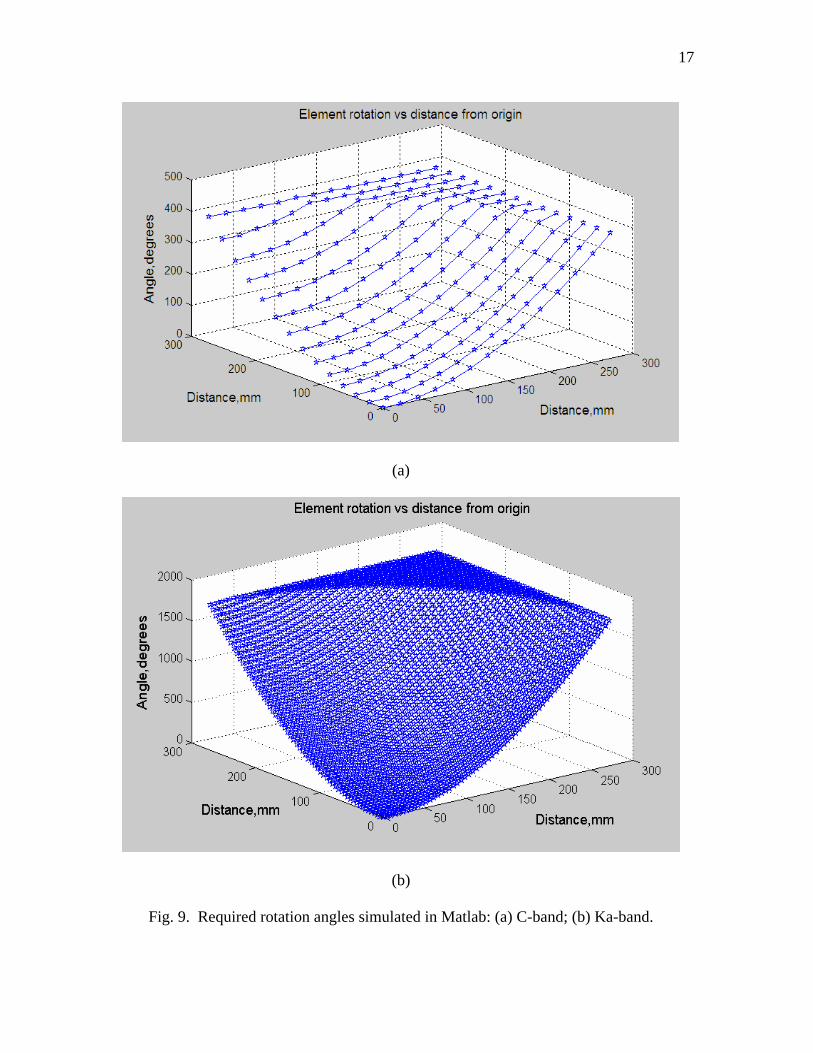
To compensate for the additional ∆l path lengths, the CP antenna arrays are rotated.
The centermost element has zero rotation since ∆l is zero at (0,0). As the elements are
placed moving away from (0,0), the variable rotation increases as shown in Figure 9. The
variable rotation ψ in radians for a circularly polarized radiator that is necessary to
compensate for ∆l is
22 o
l πψλ
∆= × (14)
degrees in the counterclockwise direction to compensate for these additional path
delays. The MATLAB code to evaluate the required rotation angles is attached in
Appendix A.
17
(a)
(b)
Fig. 9. Required rotation angles simulated in Matlab: (a) C-band; (b) Ka-band.

18
3. Circularly polarized antenna element design
A. Element design
Many different microstrip element shapes have been simulated with the aid of
Zeland’s IE3D and Ansoft’s HFSS simulator to achieve circular polarization. Although the
microstrip patch element with two delay lines is a good candidate for a CP operation, the
phase delay lines have to be very thin in order to match the input impedance of the square
patch. Moreover, to operate as a dual-band reflectarray, the top layer needs to be
transparent to the bottom layer at Ka-band. Since the ring element uses less metallization
than an equivalent patch element, it allows more incident energy to pass through between
the layers.
In this study, a simple ring structure with gaps is used to develop a dual layer CP
reflectarray. A ring structure without any gaps can resonate to the excitation of two
orthogonal field components [29]. To obtain circular polarization, however, additional
gaps are needed in the ring structure so that the reflected phase response to the excitation of
each of the two orthogonal component fields differs by 180o at the desired resonant
frequency. In other words, adding gaps in the ring enables the direction of propagation to
be reversed so that the reflected wave has same polarization as the incident wave.
Figure 10 shows the element configurations at 7.1 GHz and 32 GHz. The ring
element is simulated using the H-wall waveguide approach [30]. This approach assumes
that a uniform plane wave with a vertically polarized electric field is normally incident on
an infinite array of periodic structure. A perfect magnetic conductor and a perfect electric
conductor form the four waveguide side walls. Two simulations are performed using

19
Ansoft High Frequency Structure Simulator (HFSS) [31] with orthogonal polarizations to
determine the reflected phase and combined to extract the CP performance [32]. Figure 11
compares the simulated result of the ring element at 32 GHz with that of square patch
element with two delay lines for the right-hand CP design. Increased CP bandwidth and
left-hand CP suppression are observed for the ring element. The gap sizes are limited to
0.3 mm and 0.28 mm, respectively, due to the tolerances of fabrication in Texas A&M
facilities but would ideally be smaller.
11.5mm
0.5mm
Gap=0.3mm
10.3mm
2.26mm
0.4mm
Gap=0.28mm
(a) (b)
Fig. 10 Ring antenna elements: (a) C-band; (b) Ka-band.
-25.0
-20.0
-15.0
-10.0
-5.0
0.0
5.0
30.0 31.0 32.0 33.0 34.0
Frequency (GHz)
Cro
ss-p
olar
izat
ion
supp
ress
ion
(dB
)
RHCP, ring element
LHCP, ring element
RHCP, patch element
LHCP, patch element
Fig. 11. Comparison of cross-polarization suppression in dB at 32 GHz.
20
-180
-135
-90
-45
0
4590
135
180
225
270
315
360
0 20 40 60 80 100 120 140 160
Rotation angle (degrees)
Rel
ativ
e Ph
ase
sim
ulat
ed (d
egre
es)
RHCP at 32 GHz RHCP at 7.1GHz
LHCP at 32 GHz LHCP at 7.1 GHz
Fig. 12. Relative phase variations at a focal point referenced to zero rotation when the ring
element is rotated in the counter-clockwise direction.
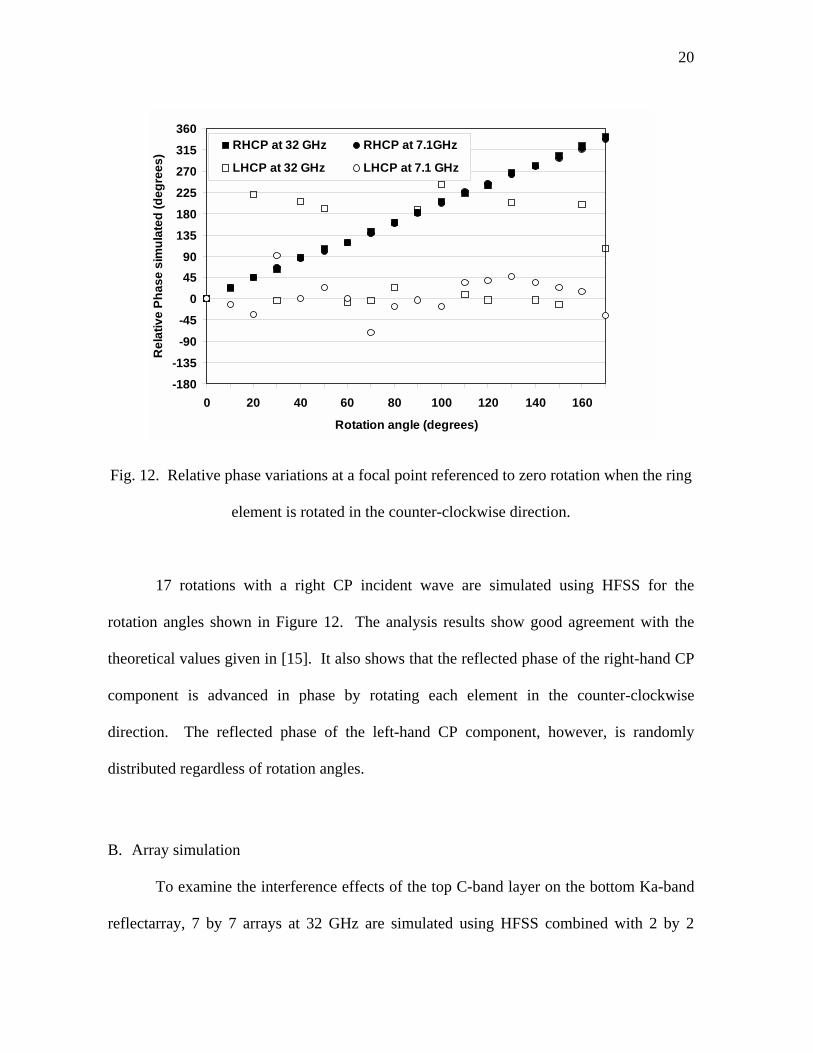
17 rotations with a right CP incident wave are simulated using HFSS for the
rotation angles shown in Figure 12. The analysis results show good agreement with the
theoretical values given in [15]. It also shows that the reflected phase of the right-hand CP
component is advanced in phase by rotating each element in the counter-clockwise
direction. The reflected phase of the left-hand CP component, however, is randomly
distributed regardless of rotation angles.
B. Array simulation
To examine the interference effects of the top C-band layer on the bottom Ka-band
reflectarray, 7 by 7 arrays at 32 GHz are simulated using HFSS combined with 2 by 2

21
arrays at 7.1GHz in the top layer. The results show that the peak gain degrades about 1 dB
in the dual layer compared to the single layer as shown in Figure 13. This 1 dB gain drop
corresponds to an efficiency drop of about 10 % at 32 GHz.
-40
-35
-30
-25
-20
-15
-10
-5
0
5
10
15
-180 -135 -90 -45 0 45 90 135 180
Angle (degrees)
Nea
r fie
ld g
ain
(dB
) of 7
by
7 ar
ray
at 3
2GH
z,
f/D=0
.7
LHCP, single layerRHCP, single layerLHCP, dual layerRHCP, dual layer
Fig. 13. 7 by 7 arrays simulated result at 32 GHz with and without the top layer of 2 by 2
arrays.

22
4. Experiments
A. C-band measurements for dual layer reflectarray
A 0.5 m diameter C-band right-hand CP planar reflectarray has been fabricated on
the top layer using 437 ring elements. The feed horn is placed at 350 mm above the center
of the reflectarray, which corresponds to a focal ratio of 0.7. The ring elements are
separated by 0.5 free space wavelengths at 7.1 GHz or 21 mm in both orthogonal directions.
This spacing provides a distance of approximately 0.25 free space wavelengths at 7.1 GHz
between the edges of adjacent ring elements.
The preliminary measurements (I) are performed in the anechoic chamber at Texas
A&M University using a circularly polarized corrugated horn as the feed antenna and a
linearly polarized standard horn as the transmit antenna. The measured phase and
magnitude information are used to determine the axial ratio of the CP reflectarray [32].
Final measurements (II) are conducted in the outdoor range at the Jet Propulsion
Laboratory (JPL) using circularly polarized corrugated horns for both the feed and transmit
antennas.
Figure 14 shows typical radiation patterns measured at A&M and JPL respectively.
Although the phase measurement done at A&M is not completely accurate, the extracted
CP gain patterns are quite similar with the patterns obtained at JPL. The peak gain is 28.2
dB (I) at 7.3 GHz and 27.8 dB (II) at 7.4GHz. The corresponding efficiency is 46% (I) and
40 % (II). Both main beams have a beam width of 5°. The peak sidelobe level is greater
than 17.3 dB (I) and 13.1 dB (II) down from the main beam and the left-hand cross
polarization level is 21 dB (I) and 27.8 dB (II) below the peak right-hand CP gain.

23
-30.0
-20.0
-10.0
0.0
10.0
20.0
30.0
-90 -75 -60 -45 -30 -15 0 15 30 45 60 75 90
Angle (degrees)
CP
gain
(dB
)
LHCP at 7.4 GHz,JPLRHCP at 7.4 GHz, JPLRHCP at 7.3 Ghz, A&MLHCP at 7.3 GHz, A&M
Fig. 14. Measured CP gains for a C band reflectarray.
The relatively large sidelobe level is, for the most part, caused by the feed horn
blockage located at the broadside direction of the reflectarray aperture. For the C band
measurements, the radiation patterns for the dual layer are not degraded compared to the
single layer case. The CP gain variations versus frequency are shown in Figure 15. The
peak gain occurs at 7.3 GHz (I) and at 7.4 GHz (II). In the measurements at JPL, the co-
polarized gain keeps increasing, but the patterns are only tested from 6.6 GHz to 7.4 GHz.
Also, both the CP horn and amplifier used in JPL operated from 8 GHz and made the cross-
polarization level unstable over frequency ranges tested.
The aperture efficiencies versus frequency are shown in Figure 16. The highest
efficiency is 46 % (I) at 7.3 GHz and 40 % at 7.4 GHz (II). Greater than 40 % efficiency is
observed between 7.1GHz and 7.4GHz in the measurements at A&M. Again, the
efficiency measured at JPL is unstable due to the operating range of the amplifier used.

24
-5
0
5
10
15
20
25
30
6.6 6.8 7 7.1 7.2 7.4
Frequency (GHz)
Co-
pol/X
-pol
gai
n (d
B) v
aria
tion
Co-pol, JPL
X-pol, JPL
Co-pol, A&M
X-pol, A&M
Fig. 15. Measured gain variations versus frequency at C-band for a dual layer.
0
5
10
15
20
25
30
35
40
45
6.6 6.8 7 7.1 7.2 7.4
Frequency (GHz)
Ape
rture
effi
cien
cy (%
)
JPL A&M
Fig. 16. Aperture efficiencies versus frequency for a dual layer.

25
0
0.5
1
1.5
2
2.5
3
6.6 6.8 7 7.1 7.2 7.4
Frequency (GHz)
Axi
al ra
tio (d
B) a
t bro
adsi
deJPL
A&M
Fig. 17. Axial ratios at broadside versus frequency for a dual layer.
The theoretical efficiency estimated is 78 % by taking the overall gain into account,
which assumes the element gain of 4 dB and the array factor of 26.4 dB. This efficiency
difference is caused by the blockage attributed to the feed antenna and its supporting metal
bars, the spillover effect due to the feed illuminating areas outside of the reflectarray, the
feed’s non-uniform illumination across the reflectarray’s aperture, scattered fields from the
edges, as well as some energy that is reflected by the array as left-handed CP.
Figure 17 shows the axial ratios at broadside versus frequency. It shows an axial
ratio less than 3 dB for all frequency ranges tested. This superior CP performance at
broadside is because the scattered and cross-polarized fields combine deconstructively due
to the element rotations. This result also shows that the given ring structure operates as a
CP antenna element by separating the co-polarized fields from the cross-polarized fields.
Figure 18 shows the reflectarray’s axial ratios versus incident angle over a frequency range

26
from 6.6 GHz to 7.4 GHz. It is observed that a plane wave can be incident upon the
reflectarray between ± 3° for all frequencies and still have the axial ratio less than 3 dB.
0
1
2
3
4
5
6
-5 -4 -3 -2 -1 0 1 2 3 4 5
Angle (degrees)
Axi
al ra
tio (d
B) v
aria
tion
6.6GHz 6.8GHz
7Ghz 7.1GHz
7.2GHz 7.4GHz
Fig. 18. Axial ratio variations versus incident angle for a dual layer.
B. Ka-band measurements for single and dual layer reflectarrays
Measurements at Ka band are conducted at JPL using circularly polarized corrugated
horns for both the feed and transmit antennas. Approximately 9200 ring elements with
variable rotations are constructed in the bottom layer. Again, the feed horn is placed at 350
mm above the center of the reflectarray aperture, which is 506 mm in diameter. The
element spacing is 0.5 free space wavelengths at 32 GHz, or 4.7 mm, in both orthogonal
directions. To assure good aperture efficiency, effort is made during measurements to
maintain the flatness of the reflectarray’s surface lest it should become delaminated.

27
-25
-15
-5
5
15
25
35
45
-45.0 -30.0 -15.0 0.0 15.0 30.0 45.0
Angle (degrees)
CP
Gai
n (d
B) a
t 31.
75 G
Hz
Co-pol, single layer
X-pol, single layer
Co-pol, dual layerX-pol, dual layer
Fig. 19. CP radiation patterns at 31.75 GHz.
Typical radiation patterns at 31.75 GHz are shown in Figure 19. The main beam has
a width of 1.3° for both the single (I) and dual layer case (II). The cross-polarization level
is 40.7 dB (I) and 29.2 dB (II) down from the peak at broadside. The sidelobe suppression
is greater than 19.5 dB (I) and 18.7 dB (II) occurring at 2°. This improved sidelobe
suppression compared to that of C band is due to the large electrical aperture size, but it is
still relatively high because of the feed blockage, edge scattering, scattering from the top
layer elements and the illumination taper of the feed horn. The peak gain varies from 41.5
dB (I) to 40.3 dB (II) causing the aperture efficiency to drop from 50 % (I) to 38 % (II).
The CP gain variations versus frequency are shown in Figure 20. The co-polarized
gain has a similar radiation pattern for both the single and dual layer cases. A large
variation in the cross-polarized gain is observed over the frequency ranges for the dual

28
layer case, but the corresponding axial ratio is still less than 3 dB.
-25
-15
-5
5
15
25
35
45
30.75 31 31.25 31.5 31.75 32 32.25 32.5 32.75
Frequency (GHz)
Co-
pol/X
-pol
gai
n (d
B) v
aria
tion
Co-pol, dual layer X-pol, dual layer
Co-pol, single layer X-pol, single layer
Fig. 20. CP gain variations versus frequency.
The measured aperture efficiencies versus frequency are shown in Figure 21. The
highest efficiency achieved is 50 % (I) and 38 % (II) at 31.75 GHz. The efficiency drop is
casued by the interference of the C-band layer. The spillover loss of -1.17 dB and aperture
nonuniform illumination loss of -0.24 dB are calculated using the definition of the
subtended angle [10] and the power pattern of the feed horn used in the measurement. A
small amount of reflectarray element loss is not measured but predicted to be -0.4 dB by
considering the equivalent dielectric and copper loss of 20 mil Duroid material [10]. The
theoretical efficiency estimated is 80 % by considering the implicit element gain of 4 dB
and the array factor of 39.6 dB. The bandwidth over 35 % efficiency is 1.5 GHz (I) and

29
250 MHz (II).
0
10
20
30
40
50
30.75 31 31.25 31.5 31.75 32 32.25 32.5 32.75
Frequency (GHz)
Ape
rture
effi
cien
cy (%
)
Single layer
Dual layer
Fig. 21. Aperture efficiencies versus frequency.
Figure 22 shows the measured axial ratios versus frequency. Excellent axial ratio
less than 0.5 dB is observed over all frequencies tested. Figure 23 shows the axial ratio
variations versus incident angle. If the plane wave at 31.75 GHz is incident upon the
reflectarray between ± 1°, the axial ratio will be better than 1.2dB.

30
0
0.5
1
1.5
2
2.5
3
30.75 31 31.25 31.5 31.75 32 32.25 32.5 32.75
Frequency (GHz)
Axi
al ra
tio (d
B)a
t bro
adsi
de
Dual layer
Single layer
Fig. 22. Axial ratios at broadside versus frequency.
0
1
2
3
4
5
6
-6.5 -5.5 -4.5 -3.5 -2.5 -1.5 -0.5 0.5 1.5 2.5 3.5 4.5 5.5 6.5
Angle (degrees)
Axi
al ra
tio (d
B) v
aria
tion
31.5GHz31.75GHz32GHz32.25GHz32.5GHz32.75GHz
Fig. 23. Axial ratio variations versus frequency for a dual layer.
31
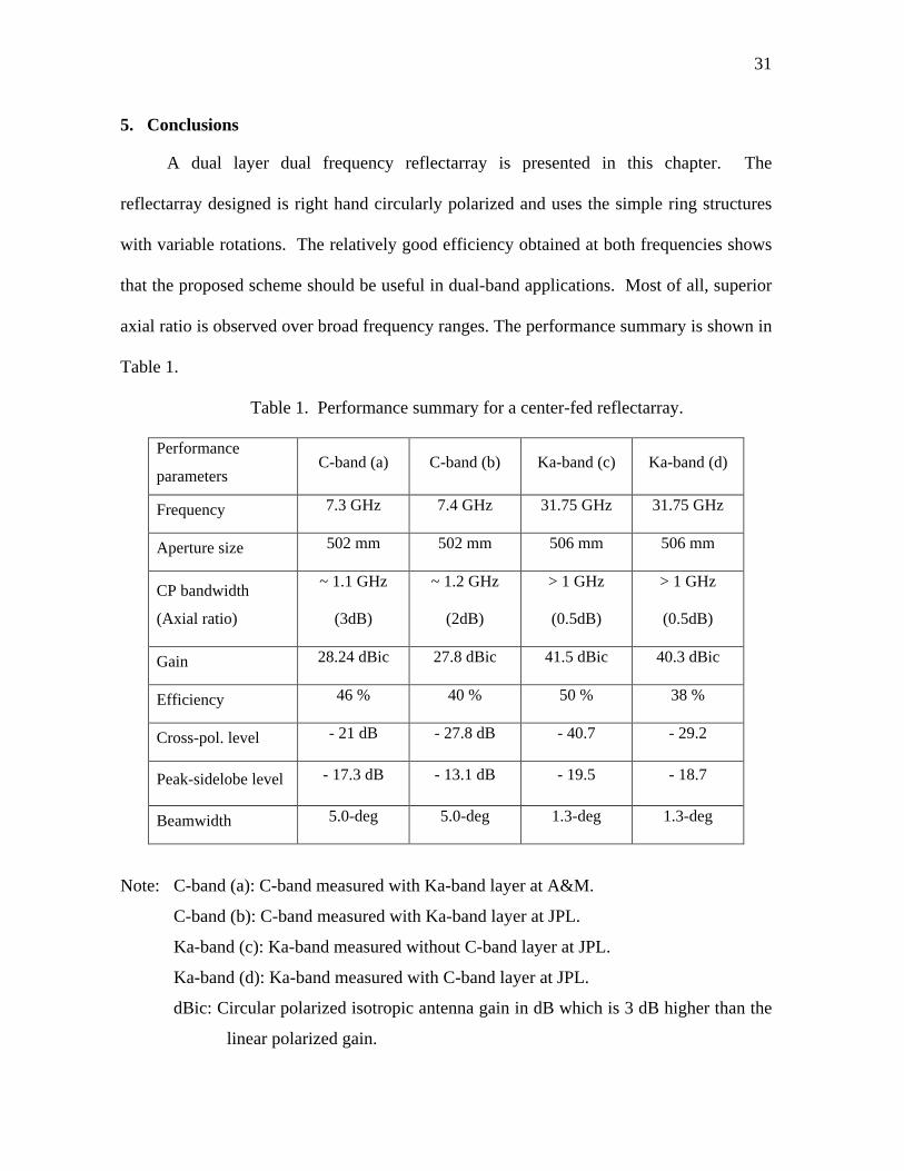
5. Conclusions
A dual layer dual frequency reflectarray is presented in this chapter. The
reflectarray designed is right hand circularly polarized and uses the simple ring structures
with variable rotations. The relatively good efficiency obtained at both frequencies shows
that the proposed scheme should be useful in dual-band applications. Most of all, superior
axial ratio is observed over broad frequency ranges. The performance summary is shown in
Table 1.
Table 1. Performance summary for a center-fed reflectarray.
Performance
parameters C-band (a) C-band (b) Ka-band (c) Ka-band (d)
Frequency 7.3 GHz 7.4 GHz 31.75 GHz 31.75 GHz
Aperture size 502 mm 502 mm 506 mm 506 mm
CP bandwidth
(Axial ratio)
~ 1.1 GHz
(3dB)
~ 1.2 GHz
(2dB)
> 1 GHz
(0.5dB)
> 1 GHz
(0.5dB)
Gain 28.24 dBic 27.8 dBic 41.5 dBic 40.3 dBic
Efficiency 46 % 40 % 50 % 38 %
Cross-pol. level - 21 dB - 27.8 dB - 40.7 - 29.2
Peak-sidelobe level - 17.3 dB - 13.1 dB - 19.5 - 18.7
Beamwidth 5.0-deg 5.0-deg 1.3-deg 1.3-deg
Note: C-band (a): C-band measured with Ka-band layer at A&M.
C-band (b): C-band measured with Ka-band layer at JPL.
Ka-band (c): Ka-band measured without C-band layer at JPL.
Ka-band (d): Ka-band measured with C-band layer at JPL.
dBic: Circular polarized isotropic antenna gain in dB which is 3 dB higher than the
linear polarized gain.
32
CHAPTER III
OFFSET-FED X/KA-BAND DUAL-BAND REFLECTARRAY
ANTENNA USING THIN MEMBRANES*
1. Introduction
In recent years, there has been a growing demand for reduced mass, small launch
volume, and at the same time, high-gain large-aperture antenna systems in space missions.
To enable deployment of large-aperture antennas, the concept of an inflatable parabolic
reflector has been proposed and experimented in the past [33-34]. However, the realization
of this concept has found difficulty in achieving and maintaining the required large, thin
curved-parabolic surface in the space environment. As an alternative to alleviate the
burden associated with curved surfaces, a new concept of using an inflatable microstrip
reflectarray antenna has been introduced by JPL in 1996 [35]. Because of the flat
reflecting surface it uses, it is believed to be more reliable in maintaining the surface
tolerance compared to its counterpart, the inflatable parabolic reflector. Although there are
still many challenges to overcome, this chapter presents an antenna component with thin
membranes to meet the demand in future inflatable antenna systems.
The reflectarray presented in this study is made of thin membranes with their
thickness equal to 0.0508 mm at both layers. It is found that if a substrate consists of only
a thin membrane, the CP bandwidth of the ring element would be significantly reduced to
* © 2005 IEEE. Parts of this chapter are reprinted, with permission, from C. Han, J. Huang, and K. Chang, “A high efficiency offset-fed X/Ka-dual-band reflectarray using thin membranes,” IEEE Trans. Antennas Propagat., vol. 53, pp. 2792-2798, Sep. 2005.
33
an unacceptable value for either X or Ka-band. In addition, there would be some increase
in substrate loss resulting in poor antenna efficiency, in particular at the Ka-band frequency.
To improve the overall performance, a new configuration is proposed by inserting empty
spaces of the proper thickness below both the X and Ka-band membranes. For this
technology demonstration, low-dielectric constant foam layers are substituted for the empty
spaces to act as support structures for the membrane layers. In an actual space flight unit,
an inflatable structure will provide proper tensioning force and support to eliminate the use
of foam layers. This study shows that, by using the new configuration, the degrading
effects of thin substrates are eliminated resulting in excellence performance for both
frequency bands. In particular, the CP bandwidth performance is significantly enhanced.
The broader CP bandwidth of the ring element plays an important role in achieving high
efficiency reflectarray performance. In addition, an offset feed scheme [36-40] is used to
reduce the blockage of the center-fed feed horn and to improve the overall efficiency. With
an offset configuration, the reaction of the reflectarray upon the primary feed horn can be
reduced to a very low order, which implies the interaction of the primary feed horn with the
reflectarray can be negligible. Also, the offset configuration can be accommodated more
easily than an axis-symmetric design in the design of spacecraft antennas. In the design,
the incidence angle of the feed horn should be carefully chosen close to the main beam
scan angle to minimize the beam-squinting properties of the circularly polarized offset
reflectarray [40]. The tested results show more than 50 % efficiencies at both frequency
ranges, which is believed to be highest efficiency ever achieved using deployable thin
membranes capable of dual-band operation.

34
A 0.5 m diameter dual-band printed reflectarray antenna designed consists of two
very thin surfaces made up of many individual rings of variable rotations and an
illuminating offset-feed as shown in Figure 24. The configuration of the dual layer
reflectarray antenna with element dimensions is also shown in Figure 25. Compared to the
Figure 10, the microstrip bar in the middle of the ring at C-band is removed since further
simulations of the ring structure found it superfluous in achieving circular polarization.
The reflectarray is fabricated on commercial Rogers R/flex 3000 liquid crystalline polymer
(LCP) material with εr = 2.9 and 0.0508 mm (2 mil) thickness for both layers. Because it is
found during simulations that the distance from the circuit layer to the ground plane should
be within 5 %-20 % of free space operating wavelengths for the given ring structure to
operate as an efficient CP, 1.6 mm foam is introduced between the Ka-band layer and the
ground plane. Also, 3.2 mm foam is placed above the Ka-band layer to separate the X-
band layer. With these foam widths, the effective substrate thickness from the circuit layer
to the ground plane becomes 0.17 free space wavelengths at 32 GHz and 0.13 free space
wavelengths at 8.4 GHz. Counter-clockwise rotations are applied to the array elements to
achieve the right-hand circular polarization for both layers. The dielectric constant of the
foam material is 1.03 (3.2 mm foam below X-band) and 1.06 (1.6 mm foam below Ka-
band) respectively, which is very close to that of air. The foam layers also have a very low
loss tangent of 0.0001.

35
(a) (b)
Fig. 24. (a) A photo of the half-meter offset-fed reflectarray with microstrip rings of
variable rotations (b) close-up view of the reflectarray element.
10 mm
Gap: 0.3 mmWidth: 0.5 mm
2.64 mm
Gap: 0.3 mmWidth: 0.4 mm
1.6 mmfoam
3.2 mmfoam
0.0508 mm (2mil)Substrate
`
Ground plane
Ka-bandarray
X-band array
Fig. 25. Two-layer reflectarray topology with element dimensions.

36
2. Offset reflecting antenna analysis
Parabolic reflector (xP, yP, zP)
Boresight axis
F ( xf , yf , zf )
Incident energy
Reflectarray (xre, yre, zre)
Feed
z
x
b
b
f
by
D
Center
DF
0ROF
O
OP
RCFz'y'
x'
O'
Fig. 26. Offset-fed reflectarray block diagram.
The analysis to calculate the needed phase delay is derived based on the comparison
of the geometrical configurations between an offset parabolic reflector and a flat microstrip
reflectarray.
The block diagram of the reflectarray with its virtual parabolic surface is shown in
Figure 26. The microstrip reflectarray elements are placed at ( , , )re re rex y z in the

37
( , , )x y z coordinate system.
Referring to Figure 26 and specifying the reflectarray’s dimension D , the vertical
distance from the reflectarray’s lower edge to the feed OFR , and the desired scan angle bθ ,
the phase center of the feed is
sin( )f OF bx R θ= − ; 0fy = ; cos( )f OF bz R θ= (15)
From the phase center of the feed, the center of the microstrip arrays on the
reflectarray’s surface is obtained such that the incident angle of the feed horn fθ relative to
the normal of the reflectarray’s surface is very close to the main beam scan angle bθ . By
choosing the value of fθ very close to bθ , the effect of beam squint with frequency can be
minimized to a great extent for an offset feed system [40].
Since the center of the microstrip arrays on the reflectarray’s surface lies on the
surface formed by the parabolic reflector, the subtended angle 0θ can be determined with
its corresponding focal length defined as [28]
0(1 cos( ))2
CFF
RD θ+= (16)
Now the origin in the ( , , )x y z coordinate system is redefined such that the phase
center ( , , )f f fx y z of the feed is placed at (0,0, )FD and the ( , , )re re rex y z coordinates of the
microstrip reflectarray elements are also transformed accordingly. Within the new

38
coordinate system, the surface of a parabolic reflector is described by the points
( , , )p p px y z and it is formed simply by expressing the value of pz coordinate in terms of
rex and rey . That is,
2 2
4re re
pF
x yzD+= (17)
Finally, the path difference is given by
2 2 2 2 2 2( ) ( )re re re F re re p F p rel x y z D x y z D z z∆ = + + − − + + − + − (18)
To compensate for the additional ∆l path lengths, The CP antenna arrays are rotated.
The center of the microstrip arrays has zero rotation since ∆l is zero. As the elements are
placed moving away from the center of arrays, the variable rotation increases. The variable
rotation ψ in radians for a circularly polarized radiator that is necessary to compensate for
∆l is
22 o
l πψλ
∆= × (19)
In this work, the following values are used to design a 0.5 m diameter reflectarray.
A. X-band
Number of ring antenna elements= 593

39
Vertical distance from the reflectarray’s lower edge to the feed, OFR = 450 mm
Focal length of the virtual parabolic reflector, FD = 407.8 mm
Physical origin of the reflectarray, ( , , )re re rex y z = (252,0,117.5) mm in the ( , , )x y z
coordinate system
Electrical origin of the reflectarray, ( , , )re re rex y z = (216,0,100.7) mm in the ( , , )x y z
coordinate system
Main beam scan angle, bθ = 25o
Incidence angle of the feed horn, fθ = 23.7o
B. Ka-band
Number of ring antenna elements= 8993
Vertical distance from the reflectarray’s lower edge to the feed, OFR = 540 mm
Focal length of the virtual parabolic reflector, FD = 489.4 mm
Physical origin of the reflectarray, ( , , )re re rex y z = (253.8,0,118.3) mm in the
( , , )x y z coordinate system
Electrical origin of the reflectarray, ( , , )re re rex y z = (258.5,0,120.5) mm in the
( , , )x y z coordinate system
Main beam scan angle, bθ = 25o
Incidence angle of the feed horn, fθ = 25.2o
Figure 27 shows the required rotation angles calculated in MATLAB with element
index starting from the bottom edge of the reflectarray’s surface.

40
(a)
(b)
Fig. 27. Required rotation angles simulated in Matlab: (a) X-band; (b) Ka-band.

41
Another consideration in the design of the offset feed reflectarray is the effect of the
feed horn pattern on the far-field pattern of the reflectarray. In a typical reflector design,
the field at the edge is approximately 10 dB below that of the center for maximum gain and
about 20 dB down for good sidelobe performance [41]. In this study, the edge taper
characteristic of 10-15 dB is aimed to compromise between the gain and the first sidelobe
level. The feed power pattern for the corrugated CP horn is characterized by commonly
used cosine-q model with q equal to 12 and the path loss is calculated based on the
geometry of the reflectarray. As a result of summing the feed taper with the path loss, the
X-band reflectarray results in an edge taper characteristic of 15.6 dB and 10.3 dB for the
upper and lower edge respectively. For the Ka-band reflectarray, 9.8 dB and 9.9 dB edge
taper are obtained for the upper and lower edge of the reflectarray.
3. Element design
The ring antenna is simulated with Ansoft’s HFSS simulator using the H-wall
waveguide approach [30] as shown in Figure 28. In the actual simulation, more attention is
given to the ring element at Ka-band because the effect of the thin substrate is most severe
at Ka-band. Figure 29 shows the simulated cross-polarization level of the ring element at
32 GHz with different thicknesses of substrate. It is observed that the CP bandwidth is
reduced significantly by using 8-mil thick substrate.
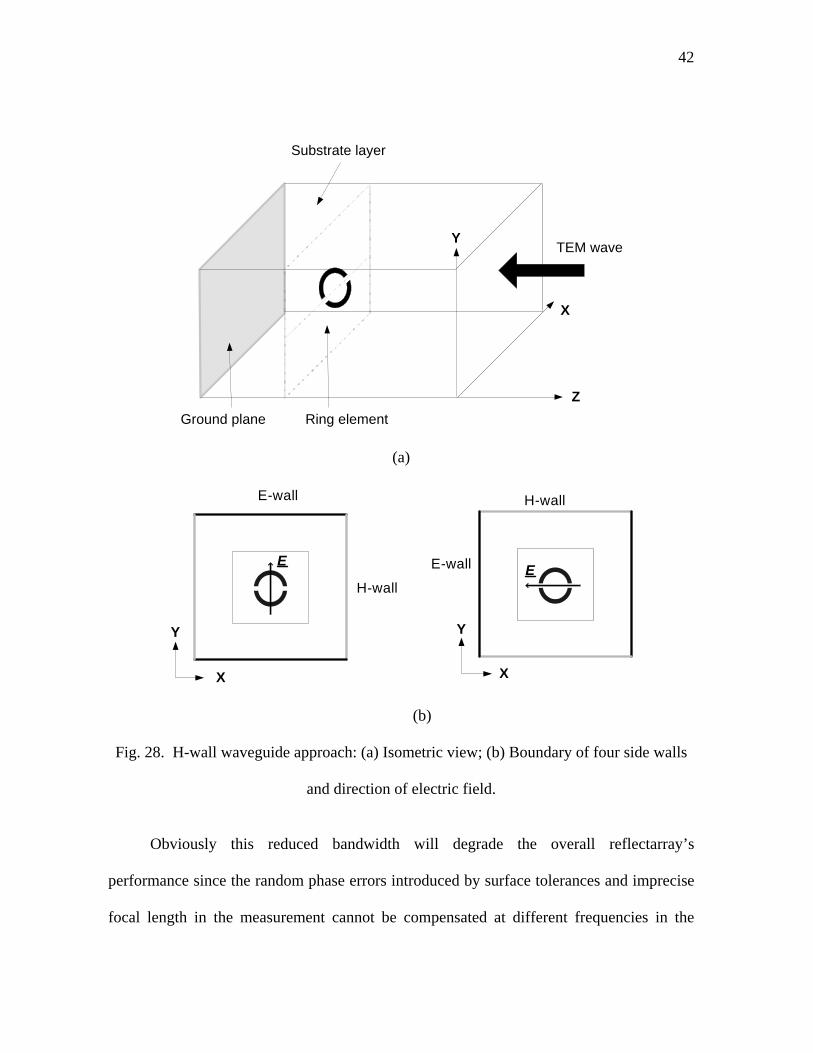
42
Ground plane
Substrate layer
Ring element
TEM wave
Z
Y
X
(a)
E-wall
H-wall
Y
X
E E-wall
H-wall
Y
X
E
(b)
Fig. 28. H-wall waveguide approach: (a) Isometric view; (b) Boundary of four side walls
and direction of electric field.
Obviously this reduced bandwidth will degrade the overall reflectarray’s
performance since the random phase errors introduced by surface tolerances and imprecise
focal length in the measurement cannot be compensated at different frequencies in the

43
vicinity of the desired frequency if the CP bandwidth of the radiating elements is too
narrow. The narrow bandwidth also imposes a very tight fabrication tolerance on the
resonant frequency of the CP element.
Besides the narrow bandwidth, it is observed that using too thin a substrate makes it
difficult to achieve circular polarization for a given ring structure with gaps because of the
weak coupling through the gaps. This phenomenon can be easily explained by a simple
simulation setup with two orthogonal excitations for the rings as shown in Figure 30.
Because little coupling occurs across each gap, it is observed that the ring element sets up a
resonance around half circumference with horizontal excitation while it resonates around
full circumference with vertical excitation [29]. So it is quite difficult to achieve circular
polarization at the desired frequency. During simulations, it is found that the effective
substrate thickness from the layer to the ground plane should be within 5 %-20 % of the
free space operating wavelength for the corresponding ring structure to operate as an
efficient CP radiator.
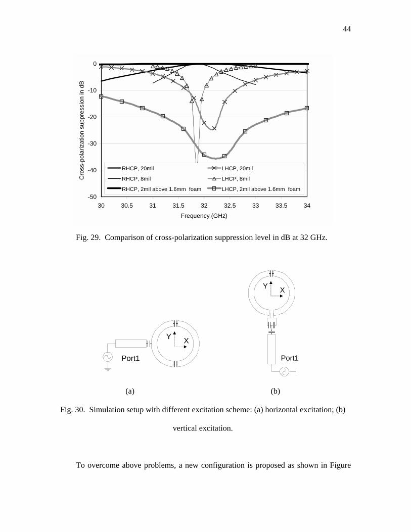
44
-50
-40
-30
-20
-10
0
30 30.5 31 31.5 32 32.5 33 33.5 34
Frequency (GHz)
Cro
ss-p
olar
izat
ion
supp
ress
ion
in d
B
RHCP, 20mil LHCP, 20mil
RHCP, 8mil LHCP, 8mil
RHCP, 2mil above 1.6mm foam LHCP, 2mil above 1.6mm foam
Fig. 29. Comparison of cross-polarization suppression level in dB at 32 GHz.
Port1
Y X
Port1
Y X
(a) (b)
Fig. 30. Simulation setup with different excitation scheme: (a) horizontal excitation; (b)
vertical excitation.
To overcome above problems, a new configuration is proposed as shown in Figure

45
25. By inserting 1.6 mm foam below the Ka-band layer, the effective substrate thickness
from the Ka-band layer to the ground plane becomes 17 % of the free space wavelength at
32 GHz. For the X-band reflectarray, 3.2 mm foam is used to separate the layers and its
effective thickness from the X-band layer to the ground plane corresponds to 13 % of the
free space wavelength at 8.4 GHz. With 0.0508 mm thick substrate in both layers and an
inserted foam below the Ka-band, the right-hand CP (RHCP) bandwidth with the left-hand
CP (LHCP) suppression is much broader at Ka-band as shown in Figure 29.
In addition to the CP bandwidth performance, using the thin substrate also increases
the loss of the reflectarray [10]. The effect of substrate loss is examined by fabricating two
0.2 m diameter Ka-band reflectarrays on different thicknesses of substrate. The first
reflectarray is etched on Rogers R/flex LCP material with εr = 2.9 and 0.2032 mm
thickness, and the second reflectarray is etched on Rogers Duroid 5870 material with εr =
2.33 and 0.508 mm thickness. The specified loss tangents given by manufacturer for the
Rogers R/flex LCP material and the Rogers Duroid 5870 material are 0.002 and 0.0012 at
10 GHz, respectively. With the ring dimensions adjusted to resonate near 32 GHz, the
reflectarrays are constructed for the same scan angle, array spacing, and focal point. The
measurement results show that the first reflectarray has the peak gain at 32 GHz, and the
second reflectarray has the peak gain at 31.5 GHz, with a peak gain difference of 3.8 dB.
Although the dielectric constant and loss tangent are different, and the highest peak gain
occurs at different frequency, this experiment shows that the thin substrate causes a
significant loss resulting in poor efficiency. Therefore, to avoid the dielectric loss of the
thin substrate, a thicker substrate is preferable, and inserting foam below the Ka-band layer
can avoid this problem.

46
4. Experiments
A. Ka-band measurements
Measurements at Ka band are conducted at Jet Propulsion Laboratory using
circularly polarized corrugated horns for both the feed and transmit antennas. 8993 ring
elements with variable rotations are constructed on the bottom layer. The ring elements are
spaced by 0.5 free space wavelengths at 32 GHz, or 4.7 mm in both orthogonal directions.
The Ka-band feed horn is placed 540 mm above the origin. The scan angle designed is 25o
in the plane of symmetry ( ' 'x z plane in Figure 26, offset plane) and 0o in the plane of
asymmetry ( ' 'y z plane in Figure 26).
In the Ka-band measurements, effort to obtain the true focus is made by way of
finding the peak gain. During the measurements, the microstrip antenna array elements
glued on the foam material are beginning to delaminate noticeably and a great deal of
attention should be paid in the future design. The highest frequency tested is 32.8 GHz due
to the operating ranges of test equipments including the corrugated CP horns.
Typical normalized radiation patterns in the plane perpendicular to the offset plane
at 32.2 GHz are shown in Figure 31. The main beam is at broadside and the 3 dB beam
width is 1.16o. The peak sidelobe levels relative to the main beam are –21.0 dB /-19.3 dB
(left/right side) for the single layer (Ka-band only without X-band layer) and –22.8 dB /-
19.9 dB (left/right side) for the dual layer (Ka-band with X-band layer). Except the peak
sidelobe occurring near the main beam, other sidelobe levels are less than –30 dB down
from the main beam. The left-hand cross-polarization level is 34 dB for the single layer
and 31.5 dB for the dual layer below the peak right-hand CP gain. Outside the main beam
region, most cross-polarization levels are suppressed fluctuating around –40 dB.
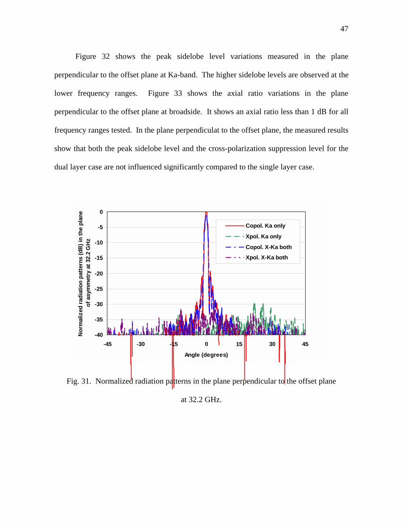
47
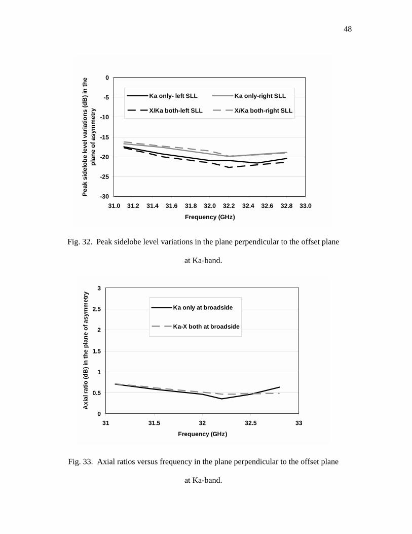
Figure 32 shows the peak sidelobe level variations measured in the plane
perpendicular to the offset plane at Ka-band. The higher sidelobe levels are observed at the
lower frequency ranges. Figure 33 shows the axial ratio variations in the plane
perpendicular to the offset plane at broadside. It shows an axial ratio less than 1 dB for all
frequency ranges tested. In the plane perpendiculat to the offset plane, the measured results
show that both the peak sidelobe level and the cross-polarization suppression level for the
dual layer case are not influenced significantly compared to the single layer case.
-40
-35
-30
-25
-20
-15
-10
-5
0
-45 -30 -15 0 15 30 45
Angle (degrees)
Nor
mal
ized
radi
atio
n pa
ttern
s (d
B) i
n th
e pl
ane
of a
sym
met
ry a
t 32.
2 G
Hz
Copol. Ka only
Xpol. Ka only
Copol. X-Ka both
Xpol. X-Ka both
Fig. 31. Normalized radiation patterns in the plane perpendicular to the offset plane
at 32.2 GHz.
48
-30
-25
-20
-15
-10
-5
0
31.0 31.2 31.4 31.6 31.8 32.0 32.2 32.4 32.6 32.8 33.0
Frequency (GHz)
Peak
sid
elob
e le
vel v
aria
tions
(dB
) in
the
plan
e of
asy
mm
etry
Ka only- left SLL Ka only-right SLL
X/Ka both-left SLL X/Ka both-right SLL
Fig. 32. Peak sidelobe level variations in the plane perpendicular to the offset plane
at Ka-band.
0
0.5
1
1.5
2
2.5
3
31 31.5 32 32.5 33
Frequency (GHz)
Axi
al ra
tio (d
B) i
n th
e pl
ane
of a
sym
met
ry
Ka only at broadside
Ka-X both at broadside
Fig. 33. Axial ratios versus frequency in the plane perpendicular to the offset plane
at Ka-band.

49
Normalized radiation patterns in the offset plane at 32.2 GHz are shown in Figure 34.
The main beam is scanned 25.6o for the single layer and 25.4o for the dual layer off the
broadside direction. The 3 dB beam width is 1.29o and 1.25o respectively. The peak
sidelobe levels are –17 dB/-18.8 dB (left/right side) for the single layer and –21 dB/-17.8
dB (left/right side) for the dual layer down from the main beam.
The left-hand cross-polarization level is 34 dB for the single layer and 31.8 dB for
the dual layer below the peak right-hand CP gain. Figure 35 shows the peak sidelobe level
variations measured in the offset plane at Ka-band. The sidelobe levels measured in the
offset plane are degraded compared to those measured in the plane perpendicular to the
offset plane with worst sidelobe level of –14 dB at 31.1 GHz. This degradation is due to
the manual alignment procedure in finding the true focal point. More specifically, given
the geometric structure of offset reflector, phase errors made by misalignment of the feed
horn give more effects in the offset plane than in the plane perpendicular to the offset plane.
The degradations include the sidelobe levels, peak gain, and the cross-polarization levels.
Figure 36 shows the axial ratio variations in the offset plane at 25o. The axial ratio is still
less than 1 dB for all frequency ranges tested.

50
-40
-35
-30
-25
-20
-15
-10
-5
0
-45 -30 -15 0 15 30 45
Angle (degrees)
Nor
mal
ized
radi
atio
n pa
ttern
s (d
B) i
n th
e pl
ane
of
sym
met
ry a
t 32.
2 G
Hz
Copol. Ka only
Xpol. Ka only
Copol. X-Ka both
Xpol. X-Ka both
Fig. 34. Normalized radiation patterns in the offset plane at 32.2 GHz.
-30
-25
-20
-15
-10
-5
0
31 31.5 32 32.5 33Frequency (GHz)
Peak
sid
elob
e le
vel v
aria
tions
(dB
) in
the
plan
e of
sym
met
ry
Ka only-left SLLKa only-right SLLX/Ka both-left SLLX/Ka both-right SLL
Fig. 35. Peak sidelobe level variations in the offset plane at Ka-band.
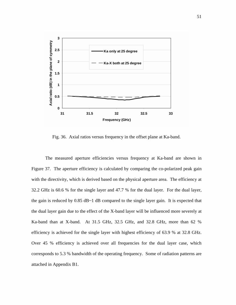
51
0
0.5
1
1.5
2
2.5
3
31 31.5 32 32.5 33
Frequency (GHz)
Axi
al ra
tio (d
B) i
n th
e pl
ane
of s
ymm
etry
Ka only at 25 degree
Ka-X both at 25 degree
Fig. 36. Axial ratios versus frequency in the offset plane at Ka-band.
The measured aperture efficiencies versus frequency at Ka-band are shown in
Figure 37. The aperture efficiency is calculated by comparing the co-polarized peak gain
with the directivity, which is derived based on the physical aperture area. The efficiency at
32.2 GHz is 60.6 % for the single layer and 47.7 % for the dual layer. For the dual layer,
the gain is reduced by 0.85 dB~1 dB compared to the single layer gain. It is expected that
the dual layer gain due to the effect of the X-band layer will be influenced more severely at
Ka-band than at X-band. At 31.5 GHz, 32.5 GHz, and 32.8 GHz, more than 62 %
efficiency is achieved for the single layer with highest efficiency of 63.9 % at 32.8 GHz.
Over 45 % efficiency is achieved over all frequencies for the dual layer case, which
corresponds to 5.3 % bandwidth of the operating frequency. Some of radiation patterns are
attached in Appendix B1.
52
0
10
20
30
40
50
60
70
31.0 31.2 31.4 31.6 31.8 32.0 32.2 32.4 32.6 32.8 33.0
Frequency (GHz)
Ape
rture
effi
cien
cy (%
)
Ka only
Ka-X both
Fig. 37. Measured aperture efficiencies versus frequency at Ka-band.
B. X-band measurements
A 0.5 m diameter X-band right-hand CP planar reflectarray has been fabricated on
the top layer using 593 ring elements. The ring elements are separated by 0.5 free space
wavelength at 8.4 GHz or 18 mm in both orthogonal directions. The X-band feed horn is
placed 450 mm above the origin (near the first element) of the X-band array elements. The
scan angle designed is 25o in the plane of symmetry ( ' 'x z plane in Figure 26, offset plane)
and 0o in the plane of asymmetry ( ' 'y z plane in Figure 26).
Typical normalized radiation patterns in the plane perpendicular to the offset plane
at 8.7 GHz are shown in Figure 38. The 3 dB beam width of the main beam at broadside is
4.4o. The peak sidelobe levels at 8.7 GHz are –23 dB/-20.5 dB (left/right side) for the
single layer (X-band only without Ka-band layer) and –24.5 dB/-20.1 dB (left/right side)
for the dual layer (X-band with Ka-band layer). The cross-polarization suppression level at

53
8.7 GHz is 21.04 dB for the single layer and 20.33 dB for the dual layer below the peak
right-hand CP gain. Other than the peak sidelobes, all the sidelobes are less than –25 dB
down from the main beam. Outside the main beam region, most cross-polarization levels
are suppressed in the ranges between –30 dB and –40 dB. The peak sidelobe level
variations in the plane perpendicular to the offset plane at X-band are shown in Figure 39.
At lower frequency ranges, a slight higher peak sidelobe level is observed for both the
single and dual layer, but the peak sidelobe level for the dual layer is not degraded
compared to the single layer case. Figure 40 shows the axial ratio variations in the plane
perpendicular to the offset plane at broadside. It shows an axial ratio less than 3 dB for all
frequency ranges tested. Best axial ratio obtained is 1.24 dB for the single layer and 1.04
dB for the dual layer at 8.5 GHz. No significant degradation is observed in the axial ratio
due to the bottom Ka-band layer.
-40
-35
-30
-25
-20
-15
-10
-5
0
-90 -75 -60 -45 -30 -15 0 15 30 45 60 75 90
Angle (degrees)
Nor
mal
ized
radi
atio
n pa
ttern
s (d
B) i
n th
e pl
ane
of a
sym
met
ry a
t 8.7
GH
z
Copol. X-only
Xpol. X-only
Copol. X-Ka both
Xpol. X-Ka both
Fig. 38. Normalized radiation patterns in the plane perpendicular to the offset plane
at 8.7 GHz.

54
-30
-25
-20
-15
-10
-5
0
8.1 8.2 8.3 8.4 8.5 8.6 8.7 8.8 8.9 9
Frequency (GHz)
Peak
sid
elob
e le
vel v
aria
tions
(dB
) in
the
plan
e of
asy
mm
etry
X only-left SLL
X only-right SLL
X/Ka both-left SLLX/Ka both-right SLL
Fig. 39. Peak sidelobe level variations in the plane perpendicular to the offset plane
at X-band.
0
1
2
3
4
5
8.1 8.2 8.3 8.4 8.5 8.6 8.7 8.8 8.9 9
Frequency (GHz)
Axi
al ra
tio (d
B) i
n th
e pl
ane
of a
sym
met
ry
X-only at broadside
X-Ka both at broadside
Fig. 40. Axial ratios versus frequency in the plane perpendicular to the offset plane
at X-band.

55
Normalized radiation patterns in the offset plane at 8.7 GHz are shown in Figure 41.
In the plane of symmetry, only the dual layer case is tested and no major effort is made to
find the right focal point. The main beam is scanned 23.13o off the broadside direction and
the 3 dB beam width is 4.55o. The measured scan angle is quite off from the designed scan
angle showing misalignment of the feed horn to the true focal point. The peak sidelobe
levels are –20.46 dB and –19.83 dB (left/right side) down from the main beam. The left
cross-polarization level is 17.6 dB below the peak right-hand CP gain, which corresponds
to the axial ratio of 2.31 dB. The peak sidelobe level variations are shown in Figure 42.
The worst peak sidelobe level measured is –15.1 dB at 8.9 GHz. The measured axial ratio
at 24o in the offset plane is shown in Figure 43. It is observed that the axial ratio is
degraded fluctuating around 3 dB showing the effect of misalignment on the axial ratio.
Less than 3 dB axial ratio is observed only from 8.5 GHz to 8.7 GHz.
-40
-35
-30
-25
-20
-15
-10
-5
0
-90 -75 -60 -45 -30 -15 0 15 30 45 60 75 90Angle (degrees)
Nor
mal
ized
radi
atio
n pa
ttern
s (d
B) i
n th
e pl
ane
of s
ymm
etry
at 8
.7 G
Hz Copol. X-Ka both
Xpol. X-Ka both
Fig. 41. Normalized radiation patterns in the offset plane at 8.7 GHz.
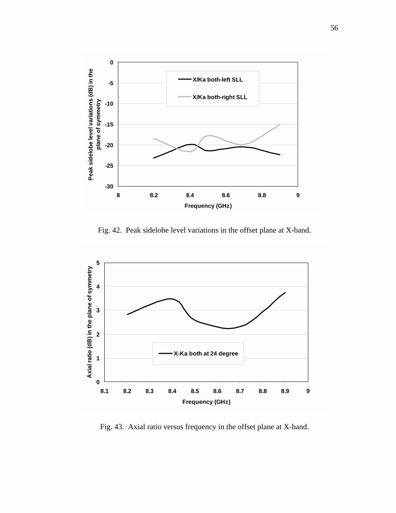
56
-30
-25
-20
-15
-10
-5
0
8 8.2 8.4 8.6 8.8 9
Frequency (GHz)
Peak
sid
elob
e le
vel v
aria
tions
(dB
) in
the
plan
e of
sym
met
ry
X/Ka both-left SLL
X/Ka both-right SLL
Fig. 42. Peak sidelobe level variations in the offset plane at X-band.
0
1
2
3
4
5
8.1 8.2 8.3 8.4 8.5 8.6 8.7 8.8 8.9 9
Frequency (GHz)
Axi
al ra
tio (d
B) i
n th
e pl
ane
of s
ymm
etry
X-Ka both at 24 degree
Fig. 43. Axial ratio versus frequency in the offset plane at X-band.

57
0
10
20
30
40
50
60
8.0 8.1 8.2 8.3 8.4 8.5 8.6 8.7 8.8 8.9 9.0
Frequency (GHz)
Ape
rture
effi
cien
cy (%
)
X-only
X-Ka both
Fig. 44. Measured aperture efficiencies versus frequency at X-band.
The measured aperture efficiencies versus frequency at X-band are shown in Figure
44. The highest efficiency is 59.2 % for the single layer and 55.4 % for the dual layer at
8.7 GHz. The peak gain for the dual layer is reduced by 0.15 dB~0.3 dB compared to the
single layer gain. Greater than 50 % efficiency is observed between 8.4 GHz and 8.8 GHz
for the dual layer. Some of radiation patterns are attached in Appendix B2.
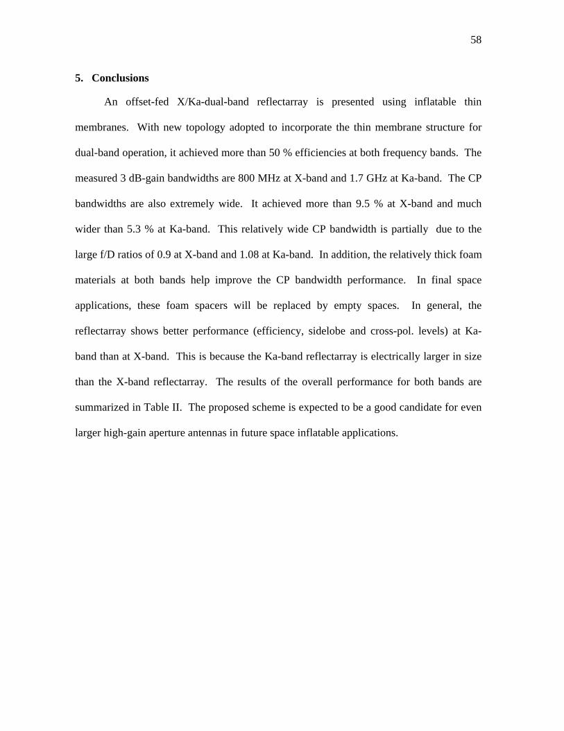
58
5. Conclusions
An offset-fed X/Ka-dual-band reflectarray is presented using inflatable thin
membranes. With new topology adopted to incorporate the thin membrane structure for
dual-band operation, it achieved more than 50 % efficiencies at both frequency bands. The
measured 3 dB-gain bandwidths are 800 MHz at X-band and 1.7 GHz at Ka-band. The CP
bandwidths are also extremely wide. It achieved more than 9.5 % at X-band and much
wider than 5.3 % at Ka-band. This relatively wide CP bandwidth is partially due to the
large f/D ratios of 0.9 at X-band and 1.08 at Ka-band. In addition, the relatively thick foam
materials at both bands help improve the CP bandwidth performance. In final space
applications, these foam spacers will be replaced by empty spaces. In general, the
reflectarray shows better performance (efficiency, sidelobe and cross-pol. levels) at Ka-
band than at X-band. This is because the Ka-band reflectarray is electrically larger in size
than the X-band reflectarray. The results of the overall performance for both bands are
summarized in Table II. The proposed scheme is expected to be a good candidate for even
larger high-gain aperture antennas in future space inflatable applications.

59
Table II. Performance summary for an offset-fed reflectarrays using thin membranes.
Performance
Parameters
X-band
only
X-band
with Ka-band
layer
Ka-band
only
Ka-band
with X-band
layer
Scan plane 0o 0o 25o 0o 25o 0o 25o
Frequency (GHz) 8.7 8.7 32.2 32.2
CP gain (dBic) 30.89 30.6 42.36 41.32
Efficiency (%) 59.2 55.4 60.6 47.0
Cross-pol. (dB) -21 -20.3 -17.6 -34 -34 -31.5 -31.8
Peak sidelobe. (dB) -20.5 -20.1 -19.8 -19.3 -17 -19.9 -17.8
Beamwidth 4.39o 4.39o 4.55o 1.16o 1.29o 1.16o 1.25o
CP bandwidth (MHz) > 800 > 800 > 500 > 1700 > 1700

60
CHAPTER IV
CASSEGRAIN OFFSET SUB-REFLECTOR-FED X/KA DUAL-BAND
REFLECTARRAY WITH THIN MEMBRANES*
1. Introduction
In recent years, there has been a growing demand for large aperture antennas in
modern communication and deep-space satellites and ground antenna systems. However,
current technology precludes the deployment of very large aperture antennas because of
weight and volume constraints. To provide cost-effective solutions featuring very low
weight and low conformable packaged volume, the concept of an inflatable reflector has
been proposed and experimented in the past [33-34]. Yet, the greatest concern to achieve
and to maintain surface shape accuracies in real implementation has prompted the
reflectarray antenna architecture which allows the use of a flat surface instead of a
parabolic antenna surface. It is believed that the flat reflecting surface is comparatively
easier to fabricate, package, and maintain in structure than a curved surface.
The objective of this study is to develop a 0.75 meter Cassegrain offset sub-
reflector-fed X/Ka dual-band reflectarray antenna using thin membranes. The use of thin
membranes has been reported in [24]. In [24], low-dielectric constant foam layers are
inserted below both the X and Ka-band membranes to act as support structures and to avoid
the risks of thin substrates. In the current work, the reflectarray is made of the same thin
* © 2006 IEEE. Parts of this chapter are reprinted, with permission, from C. Han, J. Huang and K. Chang, “Cassegrain offset sub-reflector-fed X/Ka dual-band reflectarray with thin membranes,” accepted by IEEE Trans. Antennas Propagat.

61
materials with their thickness equal to 0.0508 mm for both layers. The reflectarray utilizes
the annular ring elments to achieve circular polarization since the preceding work reported
in [21-24] showed good electrical performance. To mock-up most likely future spacecraft
launch configuration, Cassegrain offset dual-reflector system [42-53] consisting of a main
reflectarray surface and a small metallic sub-reflector feed is considered here.
One of advantages of the Cassegrain offset dual-reflector antenna [42] is the ability
to place the feed in a convenient position, while utilizing main reflector (MR) as the
focusing element. Compared with single reflector, it obtains an equivalent focal length
much greater than the physical length. In addition, dual-reflector configurations present
lower noise due to the limited noise introduced by the feed spillover beyond the sub-
reflector. This is because it is directed to cold sky rather than noisy ground as in the single
reflector case. With the addition of the sub-reflector, more degrees of freedom can be
introduced to enhance the electrical performance such as by cancelling cross-polarizations
in offset systems, or by prescribing the main aperture amplitude and phase distributions in
dual shaped reflectors.
The sub-reflector profile, which is a convex hyperboloid, has been determined
following the general design procedure presented in [52-53]. In addition to the fabrication
of the sub-reflector, two microstrip feed arrays are designed to illuminate the sub-
reflector’s surface at each frequency band. The designed microstrip patch antenna arrays
are left-hand circularly polarized so that incident wave to the main reflectarray becomes
right-handed upon reflection from the sub-reflector. As presented in [24] for dual-band
operation, same layer topology is adopted with Ka-band ring element arrays located at the
bottom layer due to the large number of elements occupied at Ka-band.

62
XSR
ZSR
YSR
O
Dsx
Dsy
SR rim
CSR
Projection of SR rim
Fo= -94.74 mm 14.57mm
164.57 mm
42.03mm
- 42.03mm
`
FO
X & Xmr
Z & Zmr
F
θθθθeαααα
ββββ
2f
θθθθe
Dm
XSR
h
Lt
Q2
Q0
Q1
dSR-mr
dF-mr
LS
P0
P2
P1
ZSR
DSX
Ht
R2
R0
R1
O
θθθθU
θθθθO
θθθθL
Lm
Reflectarray
SR
MR
Fig. 45. The offset Cassegrain geometry and the projected sub-reflector rim shape with
photo of fabricated sub-reflector.
2. Cassegrain sub-reflector design
The geometries of the offset Cassegrain antenna and the projected sub-reflector
(SR) rim shape in the SR coordinate system are shown in Figure 45 with a photo of the
fabricated sub-reflector. The parabolic main reflector is described by the diameter Dm of
its xy plane projected circular aperture, focal length F, and offset distance h. The sub-
reflector has a projected aperture in the xy plane with a major axis SXD and minor axis

63
SyD , axis tilt angle β, interfocal distance 2f, and eccentricity e. The feed parameters are
the sub-reflector edge angle θe, as observed from the reflector system focus, and the feed
pointing angle α. Two additional parameters are the clearance SR mrd − between the top of
the sub-reflector and the bottom of the main reflector, and the total length tL of the
antenna system. All the design parameters are described in Table 3.
Following the general design rule described in [52-53], all the parameters were
determined as shown in Table 4 with five initial parameters of Dm, F, h, β , and DSX. To
minimize the height of the overall antenna system, the sub-reflector was moved in
beyond the bottom edge of the main reflector resulting in negative SR mrd − value . One
thing to note that is, originally the scan angle designed was 30o in the plane of symmetry
(offset-plane, XZ-plane in Figure 45) and 0o in the plane of asymmetry and it was
initiated with respect to the boresight of the plane of the reflectarray’s surface. When
viewed with respect to the boresight of the equivalent virtual parabolic reflector’s
surface, it was re-evaluated to be 28o.

64
Table 3. Design parameters of a Cassegrain dual-reflector system [16].
Parameter Description
Dm Diameter of the MR aperture when projected on the xy plane
F Focal length of the MR
h Offset of the MR (the distance between the point Q0 on the MR coordinate system zmr
axis)
0θ Offset angle of MR
Uθ Offset angle of the top of the MR
Lθ Offset angle of the bottom of the MR
eθ Angle between the zf axis and the edge of the SR
β Tilt angle between the SR coordinate system zSR axis and the MR coordinate system
zmr axis
e SR eccentricity
a SR surface parameter
f SR surface parameter (half the interfocal distance, f=ae)
DSX Major axis of the SR elliptical aperture taken parallel to the xSR axis
DSY Major axis of the SR elliptical aperture taken parallel to the ySR axis
α Tilt angle between the SR coordinate system zSR axis and the feed coordinate system
zf axis
LS Distance between the focal point FO and the point P0 on the SR
Lm Distance between the SR point PO and the point Q0 on the MR
dSR-mr Minimum vertical distance (along the x axis) between the SR edges and the MR edges
dF-mr Minimum vertical distance (along the x axis) between the feed FO and the MR edge
Lt Maximum length (along the z axis) of the two reflector combination
Ht Maximum vertical length (along the x axis) of the two reflector combination
CSR Point expressed in the SR coordinate system defining the center of the SR elliptical
aperture

65
Table 4. Calculated design values of a Cassegrain dual-reflector system.
Step Parameter Ka-band (32 GHz) X-band (8.4 GHz)
Dm 750 mm 80 oλ 21 oλ
F 480 mm 51.2 oλ 13.44 oλ
h 480 mm 51.2 oλ 13.44 oλ
β 15 o 15o 15o
6 eθ 20.9o 20.9o
1 Oθ -53.13o -53.13o
2 Uθ -83.38o -83.38o
3 Lθ -12.48o -12.48o
4 e 2.579 2.579
7 a 18.365 mm 1.959 oλ 0.514 oλ
8 f 47.37 mm 5.053 oλ 1.326 oλ
DSX 150 mm 16 oλ 4.2 oλ
15 DSY 84.06 mm 8.96 oλ 2.354 oλ
5 α 33.22o 33.22o
9 Ls 89.68 mm 9.566 oλ 2.511 oλ
10 Lm 547.05 mm 58.35 oλ 15.317 oλ
12 dSR-mr - 0.237 mm - 6.425 oλ - 1.687 oλ
11 dF-mr 129.52 mm 13.81 oλ 3.626 oλ
13 Lt 455.07 mm 48.54 oλ 12.74 oλ
14 Ht 848.17 mm 90.47 oλ 23.75 oλ
16 CSR XcSR 9.55 oλ 2.508 oλ
ZcSR -0.583 oλ -0.153 oλ

66
3. Feed array design
Microstrip patch antenna arrays are designed to illuminate the surface of the sub-
reflector. The truncated corners square patch element is chosen to generate a left-hand
circular polarization [54]. The substrate material used is Duroid 5870 with a dielectric
constant of 2.33 with 0.7874 mm (31 mils) thickness for X-band and Duroid 5880 with a
dielectric constant of 2.2 with 0.254 mm (10 mils) thickness for Ka-band. The substrate
material is chosen considering the input VSWR and the axial ratio. When the thickness
of the substrate material is reduced, the input VSWR improves while the axial ratio
degrades [54].
In designing the microstrip patch arrays, the size of array should be carefully
selected. Table 5 shows the sub-reflector parameters to be considered in the feed array
design. SXD and SYD are the major axes of the sub-reflector’s elliptical aperture taken
parallel to the SRX , SRY axis respectively. The parameter θe is the angle between the
feed axis and the edge of the sub-reflector. SL is the distance between the feed focal
point and the center of the sub-reflector.
Table 5. Sub-reflector parameters to be considered in the feed design.
Dsx Dsy θe SL at 32 GHz SL at 8.4 GHz Sub-reflector
parameters 150 mm 84.06 mm 20.91o 9.56 oλ
(far field)
2.51 oλ
(near field)

67
Fig. 46. Normalized radiation patterns at a distance of r=2.5 oλ versus aperture size.
Assuming 2 oλ rectangular aperture size, the minimum distance to the far field
region is 8 oλ . In Table 5, by looking at the distance SL , it can be seen that the sub-
reflector lies in the far field region at Ka-band and in the near field region at X-band.
Figure 46 shows a normalized near field radiation pattern [55] for a rectangular aperture
size of a by b at a distance of 2.5 oλ at 8.4 GHz. The field over the opening is assumed
to be uniform. Initially it is expected that using a large array will take care of the
possible beam broadening effects of near field operation at X-band. However, the near
field pattern shows that although the main beam is narrower, the sidelobe level goes up
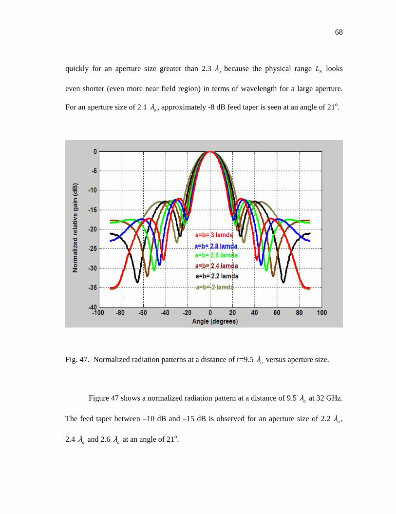
68
quickly for an aperture size greater than 2.3 oλ because the physical range SL looks
even shorter (even more near field region) in terms of wavelength for a large aperture.
For an aperture size of 2.1 oλ , approximately -8 dB feed taper is seen at an angle of 21o.
Fig. 47. Normalized radiation patterns at a distance of r=9.5 oλ versus aperture size.
Figure 47 shows a normalized radiation pattern at a distance of 9.5 oλ at 32 GHz.
The feed taper between –10 dB and –15 dB is observed for an aperture size of 2.2 oλ ,
2.4 oλ and 2.6 oλ at an angle of 21o.

69
4 by 4 feed arrays, assuming aperture size close to 2 oλ , are designed at both
bands as shown in Figure 48. With the aid of Zeland’s IE3D, first 2 by 2 subarrays are
constructed with sequential rotations to achieve a left-hand circular polarization. Then
the subarrays are one more time rotated sequentially in 0 degrees, -90 degrees, -180
degrees, and –270 degrees to improve CP bandwidth performance [56-58]. In
combining each subarray, the 360o delay lines are added in the top and bottom part of
the microstrip feed lines. The minimum line width used is 0.15 mm because of
fabrication tolerance in the etching process. The element spacing chosen is 0.588 free-
space wavelengths at X-band and 0.64 free-space wavelengths at Ka-band. The probe
feed is used to excite the microstrip antenna arrays.
L
d
X-band Ka-bandLd
o 9.375 mm35.714 mm6 mm21 mm2.99 mm11.14 mm
(a) (b)
Fig. 48. Feed arrays at both X and Ka-bands: (a) schematic of feed arrays; (b) photo of
fabricated feed arrays.
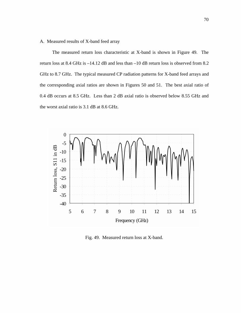
70
A. Measured results of X-band feed array
The measured return loss characteristic at X-band is shown in Figure 49. The
return loss at 8.4 GHz is –14.12 dB and less than –10 dB return loss is observed from 8.2
GHz to 8.7 GHz. The typical measured CP radiation patterns for X-band feed arrays and
the corresponding axial ratios are shown in Figures 50 and 51. The best axial ratio of
0.4 dB occurs at 8.5 GHz. Less than 2 dB axial ratio is observed below 8.55 GHz and
the worst axial ratio is 3.1 dB at 8.6 GHz.
-40
-35
-30
-25
-20
-15
-10
-5
0
5 6 7 8 9 10 11 12 13 14 15
Frequency (GHz)
Ret
urn
loss
, S11
in d
B
Fig. 49. Measured return loss at X-band.

71
-40
-35
-30
-25
-20
-15
-10
-5
0
-180 -150 -120 -90 -60 -30 0 30 60 90 120 150 180
Angle (degrees)
Nor
mal
ized
CP
radi
atio
n pa
ttern
s in
dB 8.4GHz, Copol.
8.5GHz, Copol.8.4GHz, Xpol.8.5GHz, Xpol.
Fig. 50. Normalized CP radiation patterns for X-band feed arrays.
0
0.5
1
1.5
2
2.5
3
3.5
4
8.3 8.4 8.5 8.6 8.7
Frequency (GHz)
Axi
al ra
tio in
dB
at b
ores
ight
Fig. 51. Axial ratio in dB at boresight for X-band feed arrays.

72
0
2
4
6
8
10
12
14
16
18
20
22
8.3 8.4 8.5 8.6 8.7
Freqeuency (GHz)
CP
gain
var
iatio
ns in
dB
Directivity calculated
Gain measured
Fig. 52. Gain and directivity variations versus frequency for X-band feed arrays.
Initially, the subreflector edge angle, which is observed from the reflector system
focus, was designed to be 21o. But because the actual phase center on the surface of the
sub-reflector at X-band was moved upward in the real implementation of the reflectarray,
the sub-reflector edge angle has been changed to be 15o at the upper edge and 18o at the
lower edge. In Figure 50, the far field feed taper at these angles are -7.3 dB and -8.5 dB
for both the upper and lower edge tip of the sub-reflector respectively. The gain and
directivity variations are shown in Figure 52. The directivity shown in Figure 52 is
calculated based on the measured co-polarized (left-handed) pattern. Since the CP
antenna has two orthogonal polarization components, the partial directivities, Dθ and

73
Dφ of an antenna for the θ and φ components are needed and the total maximum
directivity oD is simply sum of Dθ and Dφ . The partial directivities, Dθ and Dφ are
written as [28]
r r
4(P ) (P )ad ad
UD θθ
θ φ
π=+
(20)
r r
4(P ) (P )ad ad
UD φ
φθ φ
π=
+ (21)
Where ,U Uθ φ are radiation intensities in a given direction and r r(P ) ,(P )ad adθ φ are
total radiated powers obtained by integrating the measured radiation power pattern in a
given direction. One thing to note is that the X-band feed arrays are located at the near-
field region. In other words, the feed power pattern becomes less directive on the sub-
reflector’s edge resulting in lower spillover efficiency.
B. Measured results of Ka-band feed array
For Ka-band, good input matching is obtained at 32 GHz with the return loss of –
32 dB. The measured return loss characteristic is shown in Figure 53. The typical
measured CP radiation patterns for Ka-band feed arrays and the corresponding axial
ratios are shown in Figures 54 and 55. The best axial ratio of 0.3 dB occurs at 32.3 GHz
and less than 3 dB axial ratio is observed from 31.8 GHz to 32.6 GHz. Like the X-band,
74
the phase center on the surface of the sub-reflector at Ka-band reflectarray was moved
upward in the actual implementation of the Ka-band reflectarray. This movement occurs
because the physical center of the microstrip reflectarrays on the reflectarray’s surface
has moved upward to reduce the interaction due to the sub-reflector, which is located
beyond the bottom edge of the main reflector as shown in Figure 45. Consequently the
sub-reflector edge angle has been changed to be 14o at the upper edge and 21o at the
lower edge. In Figure 54, the far field feed taper at these angles are -6.0 dB and -15.5
dB for both the upper and lower edge tip of the sub-reflector, respectively. The gain and
directivity variations are shown in Figure 56.
-40-35
-30-25-20
-15-10
-50
10 12 14 16 18 20 22 24 26 28 30 32 34 36 38
Frequency (GHz)
Ret
urn
loss
, S11
in d
B
Fig. 53. Measured return loss at Ka-band.
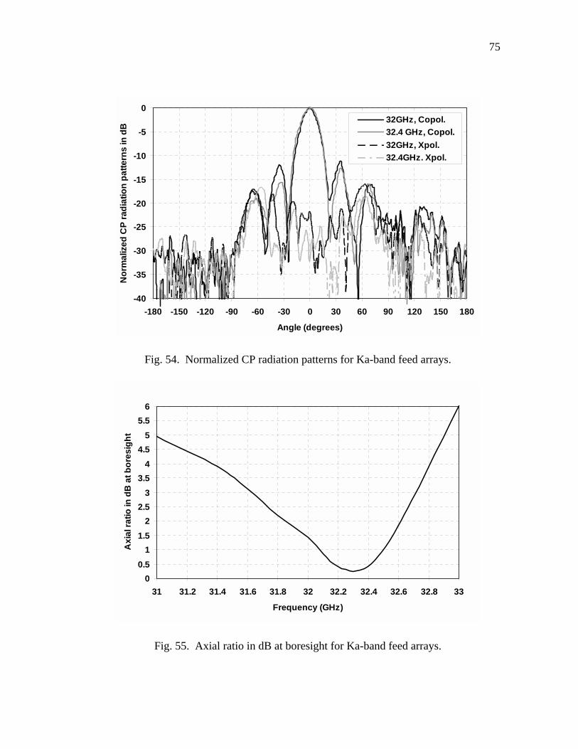
75
-40
-35
-30
-25
-20
-15
-10
-5
0
-180 -150 -120 -90 -60 -30 0 30 60 90 120 150 180
Angle (degrees)
Nor
mal
ized
CP
radi
atio
n pa
ttern
s in
dB
32GHz, Copol.32.4 GHz, Copol.32GHz, Xpol.32.4GHz. Xpol.
Fig. 54. Normalized CP radiation patterns for Ka-band feed arrays.
00.5
11.5
22.5
33.5
44.5
55.5
6
31 31.2 31.4 31.6 31.8 32 32.2 32.4 32.6 32.8 33
Frequency (GHz)
Axi
al ra
tio in
dB
at b
ores
ight
Fig. 55. Axial ratio in dB at boresight for Ka-band feed arrays.

76
0
2
4
6
8
10
12
14
16
18
20
22
31 31.2 31.4 31.6 31.8 32 32.2 32.4 32.6 32.8 33
Frequency (GHz)
CP
gain
var
iatio
ns in
dB
Directivity calculated
Gain measured
Fig. 56. Gain and directivity variations versus frequency for Ka-band feed arrays.
4. Offset reflecting antenna analysis
The analysis to calculate the needed phase delay is derived based on the
comparison of the geometrical configurations between the dual reflector system and the
flat microstrip reflectarray. The modified side view of the dual reflector system is shown
in Figure 57. The real focal point of the system is located at oF and the virtual focal
point is located at eF [48]. Since for a Cassegrain system, all parts of a wave originating
at the real focal point, and then reflected from both reflector surfaces, travel equal
distances as same as a wave originating at the virtual focal point, and then reflected from

77
the main reflector itself, the dual reflector system can be simply treated as the single-
reflector case in phase calculations with its focal point located at eF . The microstrip
reflectarray elements are placed at ( , , )re re rex y z in the ( , , )x y z coordinate system.
Fig. 57. Modified side view of the dual-reflector system.
Referring to Figure 57, and specifying the reflectarray’s dimension, the vertical
distance eOF from the reflectarray’s lower edge to the virtual feed, and the desired scan
angle bθ , the virtual phase center of the feed is
sin( )f e bx OF θ= − ; 0fy = ; cos( )f e bz OF θ= (22)

78
From the virtual phase center of the feed, the subtended angle 0θ can be
determined with its corresponding equivalent focal length defined as
0(1 cos( ))2
ee
CFf θ+= (23)
Since the center of the microstrip arrays on the reflectarray’s surface lies on the surface
formed by the parabolic reflector and the scan angle bθ is already known.
Now the origin in the ( , , )x y z coordinate system is redefined such that the virtual
phase center ( , , )f f fx y z of the feed is placed at (0,0, )ef and the ( , , )re re rex y z
coordinates of the microstrip reflectarray elements are also transformed accordingly.
The surface of a parabolic reflector is formed simply by expressing the value of pz
coordinate in terms of rex and rey . That is,
2 2
4re re
pe
x yzf
+= (24)
Finally, the path difference is given by
2 2 2 2 2 2( ) ( )re re re e re re p e p rel x y z f x y z f z z∆ = + + − − + + − + − (25)

79
One thing to note that is, originally the scan angle designed is 30o in the plane of
syemmetry (offset-plane) and 0o in the plane of asymmetry. But as indicated in Figure
57, this scan angle is with repect to the boresight of the plane of the reflectarray’s
surface. The recalculated scan angle becomes 28o when the angle is viewed with respect
to the boresight of the virtual parabolic reflector’s surface. In this study, the following
locations in the MR coordinate system in Figure 45 are used to design the flat
reflectarray as shown in Table 6.
Table 6. Locations of the reflectarray surface (units in mm).
Locations, ( , )re rex z with 0rey = Lower tip center Upper tip
Initial location at both bands (155.2,-547.5) (480,-360) (804.7,-172.5)
Modifed location at X-band (257.8, -491) (554, -320) (881.3, -131)
Modifed location at Ka-band (212.1,-517.4) (554, -320) (855.2, -146.1)
5. Experiments
A 0.75 meter reflectarray was fabricated on commercial Rogers R/flex 3000 liquid
crystalline polymer (LCP) material with εr=2.9 and 0.0508 mm (2 mils) thickness for
both layers. The ring elements are separated by 0.5 free-space wavelengths at 8.4 GHz
and 32 GHz in both orthogonal directions. The scan angle designed is 28o in the plane
of symmetry (offset-plane, ' 'x z - plane in Figure 57) and 0o in the plane of asymmetry
( ' 'y z - plane in Figure 57), which is with respect to the boresight of the virtual parabolic
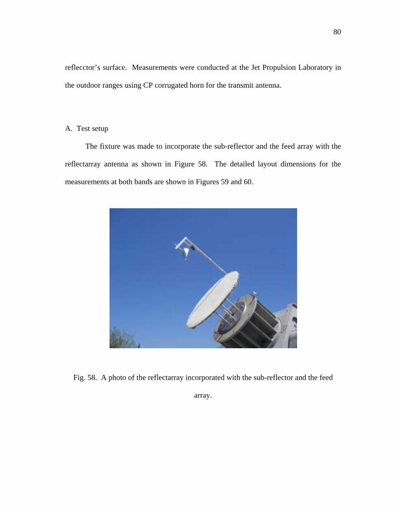
80
reflecctor’s surface. Measurements were conducted at the Jet Propulsion Laboratory in
the outdoor ranges using CP corrugated horn for the transmit antenna.
A. Test setup
The fixture was made to incorporate the sub-reflector and the feed array with the
reflectarray antenna as shown in Figure 58. The detailed layout dimensions for the
measurements at both bands are shown in Figures 59 and 60.
Fig. 58. A photo of the reflectarray incorporated with the sub-reflector and the feed
array.

81
subreflector
Metal fixture
F
X-band Reflectarray
patch 168o
750mm
9.97mm486.95mm
523.95mm
454.61mm
724.8mm
67.6mm
210.42mm 15o
18o
First reflectarray element
54.9mm
Fig. 59. Measurement layout dimensions for X-band reflectarray.
F
Ka-band Reflectarray
patch
subreflector
168o
750mm
8.03mm487.13mm
524.02mm
454.62mm
701.48mm
65.7mm
208.36mm 14o
21o
Metal fixture
First reflectarray element
Fig. 60. Measurement layout dimensions for Ka-band reflectarray.

82
B. Measured results of X-band reflectarray
Typical normalized radiation patterns at 8.4 GHz for X-band reflectarray are
shown in Figure 61. In Figure 61, the main beam (in (a)) is scanned 27o off the
broadside direction and the 3 dB beam width (in (a)) is 3.81o. The measured scan angle
is 1o off from the designed scan angle, showing the misalignment of the measured
antenna system.
X-band only
-40
-35
-30
-25
-20
-15
-10
-5
0
-90 -75 -60 -45 -30 -15 0 15 30 45 60 75 90
Angle (degrees)
Nor
mal
ized
radi
atio
n pa
ttern
s (d
B)
at 8
.4 G
Hz-
offs
et p
lane
Copol.
Xpol.
(a)
Fig. 61. Normalized CP radiation patterns at 8.4 GHz: (a) in the offset-plane for X-band
only layer; (b) in the offset-plane for both X/Ka-band layer; (c) in the plane of
asymmetry for X-band only layer; (d) in the plane of asymmetry for both X/Ka-band
layer.

83
Both X&Ka-band
-40
-35
-30
-25
-20
-15
-10
-5
0
-90 -75 -60 -45 -30 -15 0 15 30 45 60 75 90
Angle (degrees)
Nor
mal
ized
radi
atio
n pa
ttern
s (d
B)
at 8
.4 G
Hz-
offs
et p
lane
Copol.
Xpol.
(b)
X-band only
-40
-35
-30
-25
-20
-15
-10
-5
0
-90 -75 -60 -45 -30 -15 0 15 30 45 60 75 90
Angle (degrees)
Nor
mal
ized
radi
atio
n pa
ttern
s (d
B)
at 8
.4 G
Hz-
asy
mm
etric
pla
ne Copol.
Xpol.
(c)
Fig. 61. Continued.

84
Both X&Ka-band
-40
-35
-30
-25
-20
-15
-10
-5
0
-90 -75 -60 -45 -30 -15 0 15 30 45 60 75 90
Angle (degrees)
Nor
mal
ized
radi
atio
n pa
ttern
s (d
B)
at 8
.4 G
Hz-
ays
mm
etric
pla
ne Copol.
Xpol.
(d)
Fig. 61. Continued.
The peak sidelobe levels (in (a)) are 26.2 dB and 17.7 dB (left/right) down from
the main beam. The cross-polarization level (in (a)) is 28 dB below the peak right-hand
CP gain. As the frequency goes down to 8.0 GHz, the peak sidelobe level is degraded to
-15.1 dB from the main beam. However, the cross-polarization level is still suppressed
below -19 dB, which corresponds to the axial ratio of less than 2 dB. When the
frequency goes up to 8.7 GHz, the peak sidelobe level is not much changed, but the
cross-polarization level is degraded to -13.7 dB from the co-polarized beam peak.
The peak gains for the dual layer are reduced by 0.3-0.6 dB compared to the
single layer gains except for 8.4 GHz. At 8.4 GHz, the peak gain for the dual layer is
increased by 0.11 dB. This unusual increase in gain is probably due to the change of the

85
measurement setup under windy weather circumstance on the mountain. It is believed
that the rigid mounting structure is needed to improve the overall alignment process. In
the asymmetric planes of (c) and (d) in Figure 61, all the sidelobe levels are less than -30
dB and the most cross-polarization levels are suppressed below -25 dB from the co-
polarized beam peak. The aperture efficiency is calculated from the measured data by
comparing the measured co-polarized peak gain with the directivity, which is derived
based on the physical aperture area. Also, the loss factor of feed arrays in Figure 52 is
added to evaluate the pure aperture efficiency of the reflectarray itself. The measured
aperture efficiencies versus frequency are shown in Figure 62. The highest efficiency is
48.5 % for the single layer and 49.8 % for the dual layer at 8.4 GHz. Greater than 40 %
efficiency is observed between 8.2 GHz and 8.6 GHz for the dual layer case. Figure 63
shows the axial ratio variations versus frequency. It shows an axial ratio of less than 2
dB for all frequency ranges tested except for 8.7 GHz. At X-band, the size of feed
arrays is found to be relatively large compared to the size of the sub-reflector. To reduce
the possible spillover, the smaller feed arrays are advised. Some of radiation patterns are
attached in Appendix C1.

86
0
10
20
30
40
50
60
8.0 8.1 8.2 8.3 8.4 8.5 8.6 8.7
Frequency (GHz)
Ape
rture
effi
cien
cy (%
)
X-band only
X/Ka-band both
Fig. 62. Aperture efficiencies versus frequency at X-band.
0.0
0.5
1.0
1.5
2.0
2.5
3.0
3.5
4.0
4.5
5.0
8.0 8.1 8.2 8.3 8.4 8.5 8.6 8.7
Frequency (GHz)
Axi
al ra
tio (d
B)
Offset-plane, X-band only
Offset-plane, X/Ka-band both
Asymmetric-plane, X-band only
Asymmetric-plane, X/Ka-band both
Fig. 63. Axial ratios versus frequency at X-band.

87
C. Measured results of Ka-band reflectarray
Typical normalized radiation patterns at 31.8 GHz for Ka-band reflectarray are
shown in Figure 64. For the Ka-band only layer in the offset-plane, the main beam (in
(a)) is scanned 28.2o off the broadside direction and the 3 dB beam width is 1.08o. The
measured scan angle is very close to the desired scan angle.
Ka-band only
-40
-35
-30
-25
-20
-15
-10
-5
0
-90 -75 -60 -45 -30 -15 0 15 30 45 60 75 90
Angle (degrees)
Nor
mal
ized
radi
atio
n pa
ttern
s (d
B)
at 3
1.8
GH
z- o
ffset
pla
ne
Copol.
Xpol.
(a)
Fig. 64. Normalized CP radiation patterns at 31.8 GHz: (a) in the offset-plane for Ka-
band only layer; (b) in the offset-plane for both X/Ka-band layer; (c) in the plane of
asymmetry for Ka-band only layer; (d) in the plane of asymmetry for both X/Ka-band
layer.

88
Both Ka & X-band
-40
-35
-30
-25
-20
-15
-10
-5
0
-90 -75 -60 -45 -30 -15 0 15 30 45 60 75 90
Angle (degrees)
Nor
mal
ized
radi
atio
n pa
ttern
s (d
B)
at 3
1.8
GH
z- o
ffset
pla
ne
Copol.
Xpol.
(b)
Ka-band only
-40
-35
-30
-25
-20
-15
-10
-5
0
-30 -25 -20 -15 -10 -5 0 5 10 15 20 25 30
Angle (degrees)
Nor
mal
ized
radi
atio
n pa
ttern
s (d
B)
at 3
1.8
GH
z- a
sym
met
ric p
lane Copol.
Xpol.
(c)
Fig. 64. Continued.
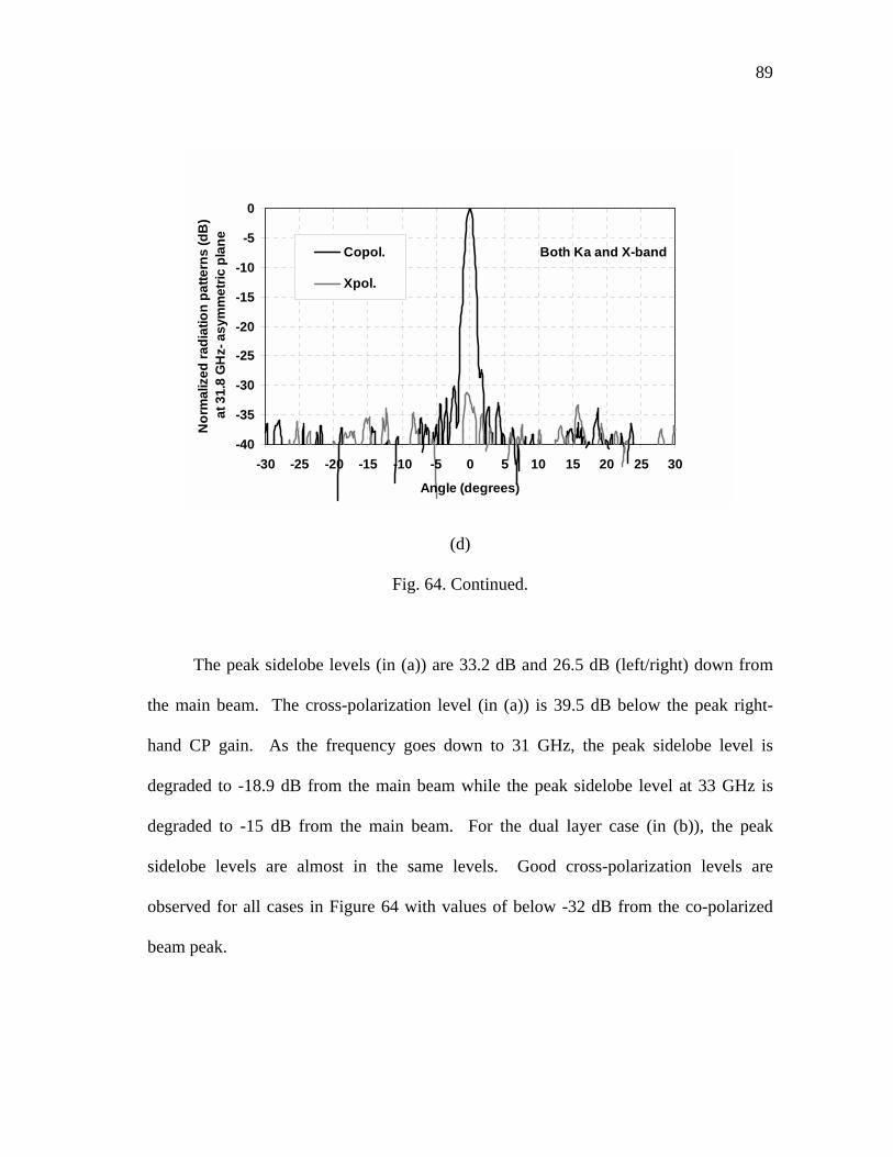
89
Both Ka and X-band
-40
-35
-30
-25
-20
-15
-10
-5
0
-30 -25 -20 -15 -10 -5 0 5 10 15 20 25 30
Angle (degrees)
Nor
mal
ized
radi
atio
n pa
ttern
s (d
B)
at 3
1.8
GH
z- a
sym
met
ric p
lane
Copol.
Xpol.
(d)
Fig. 64. Continued.
The peak sidelobe levels (in (a)) are 33.2 dB and 26.5 dB (left/right) down from
the main beam. The cross-polarization level (in (a)) is 39.5 dB below the peak right-
hand CP gain. As the frequency goes down to 31 GHz, the peak sidelobe level is
degraded to -18.9 dB from the main beam while the peak sidelobe level at 33 GHz is
degraded to -15 dB from the main beam. For the dual layer case (in (b)), the peak
sidelobe levels are almost in the same levels. Good cross-polarization levels are
observed for all cases in Figure 64 with values of below -32 dB from the co-polarized
beam peak.

90
The peak gains for the dual layer are reduced by 1.0-1.3 dB compared to the
single layer gains across the measured frequency ranges. In the asymmetric plane of (c)
and (d), all the sidelobe levels are less than -28.5 dB, which is believed to be under-
illuminated. Further considerations on the illumination taper are recommended to
increase the overall aperture efficiency. The measured aperture efficiencies versus
frequency are shown in Figure 65 after taking consideration of the loss factor in Figure
56. The highest efficiency is 64.4 % for the single layer and 48.2 % for the dual layer at
31.8 GHz. The corresponding gain variations are within ± 0.65 dB from the nominal
value throughout the frequency ranges tested. This constant gain over frequencies is due
to two factors. For example, at higher frequency, the aperture size of the feed arrays is
electrically large producing the narrower beam pattern. Then, it is expected that on the
surface of the main reflectarray, a sinc function-like surface current is generated and
when Fourier transformed to form the far-field pattern, the resulting main beam lobe
becomes broader. However, there exists less spillover due to a sine function-like surface
current. As a result, these two factors compromise each other to establish the constant
gain over frequencies. The phenomena at lower frequency can be explained vice versa.
Figure 66 shows the axial ratio variations versus frequency. Excellent axial ratios of less
than 0.7 dB are observed over all frequency ranges tested. Some of radiation patterns
are attached in Appendix C2.

91
0
10
20
30
40
50
60
70
31.4 31.6 31.8 32.0 32.2 32.4 32.6 32.8 33.0
Frequency (GHz)
Ape
rture
effi
cien
cy (%
)
Ka-band only
X/Ka-band both
Fig. 65. Aperture efficiencies versus frequency at Ka-band.
0.0
0.5
1.0
1.5
2.0
2.5
3.0
31.0 31.5 32.0 32.5 33.0
Frequency (GHz)
Axi
al ra
tio (d
B)
Offset-plane, X-band only
Offset-plane, X&Ka-band both
Asymmetric-plane, X-band only
Asymmetric-plane, X&Ka-bandb th
Fig. 66. Axial ratios versus frequency at Ka-band.

92
6. Conclusions
A 0.75 meter Cassegrain offset sub-reflector-fed X/Ka dual-band reflectarray
using thin membranes is presented for the first time in this work. The sub-reflector is
fabricated using combinations of prescribed geometric parameters and two separate
microstrip feed arrays at each band are designed to illuminate the sub-reflector’s surface.
The measured peak efficiencies are 49.8 % at X-band and 48.2 % at Ka-band. The
measured patterns are well behaved with relatively low cross-pol. and sidelobe levels, in
particular for the Ka-band results. The CP bandwidths are more than 8 % at X-band and
far more than 6 % at Ka-band, which is significantly wider than those of the fabricated
feed arrays. In other words, the reflectarray lends itself to good CP performance even
for the narrower CP bandwidth feed arrays because the cross-pol. radiations from all
elements are diffused using the angular rotations. The reflectarray’s peak gains are
reduced by approximately 1.2 dB at Ka-band and 0.5 dB at X-band due to the existence
of other layer. However, the gain variations are within ± 0.65 dB from the nominal
value for both bands through the tested frequency ranges.
With further optimization, there is room for improvements and it is expected to be
a good candidate that can be implemented in real system in no time. Several problems
encountered in this study are: First, the mounting structure needs to be improved for the
sub-reflector and feed arrays to survive in heavy wind environment. Second, the thin
film spacing needs to be more uniformly distributed, especially for Ka-band reflectarray.
Third, for the X-band reflectarray, the 4 by 4 feed array seems to be too large in size

93
relative to the size of the sub-reflector, which means high spillover on the surface of the
sub-reflector. For this reason, 3 by 3 feed arrays or larger sub-reflector are desirable to
improve the overall X-band aperture efficiency. The performance summary is shown in
Table 7.
Table 7. Performance summary of a Cassegrain offset-fed reflectarray.
Parameters X-band only
(single-layer)
X-band
(dual-layer)
Ka-band
(single-layer)
Ka-band
(dual-layer)
Scan plane 0o 28o 0o 28o 0o 28o 0o 28o
Frequency (GHz) 8.4 8.4 31.8 31.8
CP gain (dBic) 33.25 33.36 45.99 44.73
Efficiency (%) 48.5 49.8 64.4 48.2
X-pol. level (dB) 26.6 28 25.6 27.4 32.2 39.5 33.0 37.7
Peak sidelobe. (dB) 32.1 17.7 28.5 17.9 32.5 26.5 30.2 26.3
Beamwidth 3.48o 3.81o 3.58o 3.89o 0.95o 1.08o 0.94o 1.10o
CP Bandwidth (MHz) > 600 > 600 > 2000 > 2000

94
CHAPTER V
SUMMARY AND RECOMMENDATIONS
1. Summary
With the advancement of space exploration, there is an increasing demand for
larger aperture antennas with very small masses and launch volumes. As one of the
solutions, deployable antenna technology using inflatable structures and thin membranes
has recently being investigated, particularly, the technology of inflatable flat reflectarray.
The reflectarray, however, suffers from limited bandwidth typically less than 10 %.
In this dissertation, A series of developments have been carried out to demonstrate
the dual-band capability of the reflectarray to meet the multi-band requirements. First, a
0.5 meter center-fed C/Ka dual-band reflectarray has been successfully developed. This
reflectarray used annular ring elements with the angular rotation technique to achieve the
required phase delays for circular polarization. A subsequent development for an offset
–fed configuration was also successfully demonstrated using two-layer thin membranes.
Finally, a Cassegrain offset-fed X/Ka dual-band reflectarray with a 0.75 meter diameter
was successfully developed using two-layer thin membranes. For very large apertures,
Cassegrain offset-fed configuration, in addition to minimizing the feed blockage, would
allow the feed and its associated electronics to be located close to the spacecraft for
easier thermal control, in particular, when minimizing of RF loss in the feed cable is in
consideration. This Cassegrain dual-band technology presented in this dissertation is

95
currently being implemented onto a 3 meter reflectarray with inflatable structures and is
planned for application to an 8 meter inflatable reflectarray in the near future.
2. Recommendations for future research
Further optimizations in the analysis of reflector antenna with various feed
arrangements are suggested for performance improvements in the future. The gain loss
of a Ka-band reflectarray due to the interference of the top X-band reflectarray needs
more study to reduce the performance degradation at Ka-band. A Ka-band reflectarray
which was in the bottom in this study can be positioned in the top layer to investigate the
further improvements. A dual-band CP reflectarray may be constructed on the single
layer using the proposed annular ring elements. Because there exist some restrictions in
the element spacings in order to share the same layer, careful attention needs to be given
when choosing the most favorable two frequency bands. A triple-band reflectarray can
be done using the annular rings if there are applications. A study for a dual-band
linearly polarized reflectarray made of thin membranes needs to be followed for the LP
applications. Since the angular rotation technique is not applicable for the LP
applications and the required phase curves are more vulnerable to the substrate’s
thickness, a new type of element needs to be developed in this case. For example,
currently, a Ku/Ka dual-band reflectarray is being investigated for the NASA Titan
Cloud Precipitation Radar and Altimeter (TCPRA) system. The reflectarray supports
dual-linear polarizations with both vertical and horizontal polarizations, while the feed
arrays are 0.5 meter long microstrip arrays with single linear polarization.

96
REFERENCES
[1] Marco A. B. Terada, “Reflector antennas,” Encyclopedia of RF and Microwave
Engineering, edited by K. Chang, vol. 5, pp 4450-4474, John Wiley & Sons,
New York, 2005.
[2] J. Huang, “Reflectarray antenna,” Encyclopedia of RF and Microwave Engineering,
edited by K. Chang, vol. 5, pp 4428-4436, John Wiley & Sons, New York, 2005.
[3] R. E. Munson and H. Haddad, “Microstrip reflectarray for satellite communication
and RCS enhancement and reduction,” U.S. Patent 4 684 952, Washington, DC,
Aug. 1987.
[4] J. Huang, “Microstrip reflectarray antenna for the SCANSCAT radar application,” Jet
Propulsion Lab., Pasadena, CA, No. 90-45, Nov. 1990.
[5] R. D. Javor, X. D. Wu, and K. Chang, “Offset-fed microstrip reflectarray antenna,”
Electron. Lett., vol. 30, pp. 1363-1365, Aug. 1994.
[6] R. D. Javor, X. Wu, and K. Chang, “Design and performance of a microstrip
reflectarray antenna,” IEEE Trans. Antennas Propagat., vol. 43, pp. 932-939,
Sept. 1995
[7] D. M. Pozar and T. A. Metzler, “Analysis of a reflectarray antenna using microstrip
patches of variable size,” Electron. Lett., vol. 29, pp. 657-658, Apr. 1993.
[8] D. C. Chang and M. C. Huang, “Multiple polarization microstrip reflectarray antenna
with high efficiency and low cross-polarization,” IEEE Trans. Antennas

97
Propagat., vol. 43, pp. 829-834, Aug. 1995.
[9] S. D. Targonski, D. M. Pozar, and H. D. Syrigos, “Analysis and design of millimeter
wave microstrip reflectarrays,” in Proc. IEEE AP-S Symp., June 1995, vol. 1, pp.
578-581.
[10] D. M. Pozar, S. D. Targonski, and H. D. Syrigos, “Design of millimeter wave
microstrip reflectarrays,” IEEE Trans. Antennas Propagat., vol. 45, pp. 287-296,
Feb. 1997.
[11] D. M. Pozar, S. D. Targonski, and R. Pokuls, “A shaped-beam microstrip patch
reflectarray,” IEEE Trans. Antennas Propagat., vol. 47, pp. 1167-1173, July
1997.
[12] J. A. Encinar, “Design of two-layer printed reflectarrays using patches of variable
size,” IEEE Trans. Antennas Propagat., vol. 49, pp. 1403-1410, Oct. 2001.
[13] D. M. Pozar and S. D. Targonski, “A microstrip reflectarray using crossed dipoles,”
in Proc. IEEE AP-S Symp., June 1998, vol. 2, pp. 1008-1011.
[14] J. Shaker and M. Cuhaci, “Planar reflector for LMCS application,” Electron. Lett., vol.
35, pp. 103-104, Jan. 1999.
[15] J. Huang and R. Pogorzelski, “A Ka-band microstrip reflectarray with elements
having variable rotation angles,” IEEE Trans. Antennas Propagat., vol. 46, pp.
650-656, May 1998.
[16] J. Huang, “Capabilities of printed reflectarray antennas,” in Proc. IEEE Int. Symp.

98
Phased Array Systems Technology, Oct. 1996, pp. 131-134.
[17] J. Huang, “Bandwidth study of microstrip reflectarray and a novel phased reflectarray
concept,” in Proc. IEEE AP-S Symp., June 1995, vol. 1, pp. 582-585.
[18] D. M. Pozar, “Bandwidth of reflectarrays,” Electron. Lett., vol. 39, pp. 1490-1491,
Oct. 2003.
[19] D. I. Wu, R. C. Hall, and J. Huang, “Dual-frequency microstrip reflectarray,” in Proc.
IEEE AP-S Symp., June 1995, vol. 4, pp. 2128-2131.
[20] J. A. Encinar, “Design of a dual frequency reflectarray using microstrip stacked
patches of variable size,” Electron. Lett., vol. 32, pp. 1049-1050, June 1996.
[21] C. Han and K. Chang, “Ka-band reflectarray using ring elements,” Electron. Lett., vol.
39, pp. 491-493, Mar. 2003.
[22] B. Strassner, C. Han, and K. Chang, “Circularly polarized reflectarray with microstrip
ring elements having variable rotation angles,” IEEE Trans. Antennas Propagat.,
vol. 52, pp. 1122-1125, Apr. 2004.
[23] C. Han, C. Rodenbeck, J. Huang, and K. Chang, “A C/Ka dual frequency dual layer
circularly polarized reflectarray antenna with microstrip ring elements,” IEEE
Trans. Antennas Propagat., vol. 52, pp. 2871-2876, Nov. 2004.
[24] C. Han, J. Huang, and K. Chang, “A high efficiency offset-fed X/Ka-dual-band
reflectarray using thin membranes,” IEEE Trans. Antennas Propagat., vol. 53, pp.
2792-2798, Sep. 2005.

99
[25] J. Huang, C. Han, and K. Chang, “A Cassegrain offset-fed dual-band reflectarray.” to
be presented at IEEE AP-S/URSI Symp., Albuquerque, July 2006.
[26] C. Han, J. Huang, and K. Chang, “Cassegrain offset sub-reflector-fed X/Ka dual-band
reflectarray with thin membranes,” in preparation, June 2006.
[27] R. P. Jedlicka, M. T. Poe, and K. R. Carver, “Measured mutual coupling between
microstrip elements,” IEEE Trans. Antennas Propagat., vol. 29, pp. 147-149, Jan.
1981.
[28] C. Balanis, Antenna Theory, Wiley & Sons, New York, 1982, chap. 15.
[29] K. Chang, Microwave Ring Circuits and Antennas, Wiley & Sons, New York, 1996,
chap. 2.
[30] M. E. Bialkowsk and F. E. Tsai, “A unit cell waveguide model of a reflectarray
formed by microstrip patches and slots,” Microwave and Optical Technology
Letters, vol 36, pp. 206-210, Feb. 2003.
[31] HFSS ver. 8.0, Ansoft Inc., Four Station Square- Suite 200, Pittsburgh, PA 15219-
1119.
[32] B. Y. Toh, R. Cahill, and V. F. Fusco, “Understanding and measuring circular
polarization,” IEEE Trans. Antennas Propagat., vol. 46, pp. 313-318, Aug. 2003.
[33] M. Thomas and G. Veal, “Highly accurate inflatable reflectors,” Report AFRPL Tr.
84-023, May 1984.
[34] R. E. Freeland, G. D. Bilyeu, and G. R. Veal, “Large inflatable deployable antenna

100
flight experiment results,”, in 48th Congress of the International Astronautical
Federation, Turin, Italy, Oct. 1997, IAF Paper 97-1.3.01.
[35] J. Huang and A. Feria, “A 1-m X-band inflatable reflectarray antenna,” Microwave
and Optical Technology Letters, vol. 20, pp. 97-99, Jan. 1999.
[36] A. W. Rudge and N. A. Adatia, “Offset-parabolic-reflector antennas,” in Proc. IEEE
AP-S Symp., Dec. 1978, vol. 66, pp. 1592-1618.
[37] A. C. Ludwig, “The definition of cross polarization,” IEEE Trans. Antennas
Propagat., vol. 21, pp. 116-119, Jan. 1973.
[38] W. Stutzman and M. Terada, “Design of offset-parabolic-reflector antennas for low
cross-pol and low sidelobes,” in IEEE Antennas Propagat. Magazine, vol. 35, pp.
46-49, Dec. 1993.
[39] Y. Rahmat-Samii, R. A. Hoferer, and H. Mosallaei, “Beam efficiency of reflector
antennas: The simple formula,” in IEEE Antennas and Propagation Magazine,
Vol. 40, pp 82-87, Oct. 1988.
[40] S. D. Targonski and D. M. Pozar, “Minimization of beam squint in microstrip
reflectarrays using an offset feed,” in Proc. IEEE AP-S Symp., July 1996, vol. 2,
pp. 1326-1329.
[41] R. C. Johnson, Antenna Engineering Handbook, McGraw-Hill, New York, 1993,
chap. 17.
[42] P. W. Hannan, “Microwave antennas derived from the Cassegrain telescope,” IRE
101
Trans. Antennas Propagat., vol. 9, pp. 140-153, Mar. 1961.
[43] G. W. Collins “Shaping of subreflectors in Cassegrainian antennas for maximum
aperture efficiency,” IEEE Trans. Antennas Propagat., vol. 21, pp. 309-313, May
1973.
[44] Y. Mizuguch, M. Akagawa, and H. Yokoi, “Offset dual reflector antenna,” in Proc.
IEEE AP-S Int. Symp. Dig., Oct. 1976, vol. 14, pp. 2-5.
[45] V. Jamnejad-Dailami and Y. Rahmat-Samii, “Some important geometrical features of
conic-section-generated offset reflector antennas,” IEEE Trans. Antennas
Propagat., vol. 28, pp. 952-957, Nov. 1980.
[46] R. A. Shore, “A simple derivation of the basic design equation for offset dual
reflector antennas with rotational symmetry and zero cross polarization,” IEEE
Trans. Antennas Propagat., vol. 33, pp.114-116, Jan. 1985.
[47] Y. Rahmat-Samii, “Subreflector extension for improved efficiencies in Cassegrain
antennas- GTD/PO analysis,” IEEE Trans. Antennas Propagat., vol. 34, pp.
1266-1269, Oct. 1986
[48] W. V. T. Rusch, A. Prata, Jr., Y. Rahmat-Samii, and R. A. Shore, “Derivation and
application of the equivalent paraboloid for classical offset Cassegrain and
Gregorian antennas,” IEEE Trans. Antennas Propagat., vol. 38, pp. 1141-1149,
Aug. 1990.
[49] K. W. Brown and A. Prata, Jr., “A design procedure for classical offset dual reflector

102
antennas with circular apertures,” IEEE Trans. Antennas Propagat., vol. 42, pp.
1145-1153, Aug. 1994.
[50] C. Granet, “Designing axially symmetric Cassegrain or Gregorian dual-reflector
antennas from combinations of prescribed geometric parameters,” IEEE
Antennas and Propagation Magazine, Vol. 40, pp 76-82, Apr. 1998.
[51] C. Granet, “A simple procedure for the design of Classical displaced-axis dual-
reflector antennas using a set of geometric parameters,” IEEE Antennas and
Propagation Magazine, Vol. 41, pp 64-71, Dec. 1999.
[52] C. Granet, “Designing classical offset cassegrain or Gregorian dual-reflector antennas
from combinations of prescribed geometric parameters,” IEEE Antennas and
Propagation Magazine, Vol. 44, pp 114-123, June 2002.
[53] C. Granet, “Designing classical offset cassegrain or Gregorian dual-reflector antennas
from combinations of prescribed geometric parameters- Part 2: feed-horn
blockage conditions,” IEEE Antennas and Propagation Magazine, Vol. 45, pp
86-89, Dec. 2003.
[54] P. C. Sharma and K. C. Gupta, “Analysis and optimized design of single point feed
circularly polarized microstrip antennas,” IEEE Trans. Antennas Propagat., vol.
31, pp. 949-955, Nov. 1983.
[55] Y. T. Lo, and S. W. Lee, Antenna Handbook: theory, applications, and design, New
York: Van Nostrand Reinhold, New York, 1988, chap. 5.

103
[56] T. Teshirogi, M. Tanaka, and W. Chujo, “Wideband circularly polarized array
antenna with sequential rotation and phase shifts of elements,” in Proc. IEEE
AP-S Int. Symp., Aug. 1985, vol. 1, pp 117-120.
[57] J. Huang, “A technique for an array to generate circular polarization with linearly
polarized elements,” IEEE Trans. Antennas Propagat., vol. 34, pp. 1113-1124,
Sept. 1986.
[58] J. Huang, “A Ka-band circularly polarized high-gain microstrip array antenna,” IEEE
Trans. Antennas Propagat., vol. 43, pp.113-116, Jan. 1995.

104
APPENDIX A
A1. MATLAB code to create the required phase of the reflectarray element clear; % clears all variables from previous execution
clc; % clears command terminal
% user input variables
at=input('Enter 1 for square and 2 for circle ');
if at~=1&at~=2
sprintf('%d an invalid array type!!',at)
else
frg=input('Enter the reflectarray operating frequency in GHz ');
f=input('Enter the focal length from the reflector in mm ');
d=input('Enter the diameter of the parabolic reflector in mm ');
dx=input('Enter the element spacing in the x direction in mm ');
dy=input('Enter the element spacing in the y direction in mm ');
fr=frg*1e9; % frequency in Hz
c=3e8; % speed of light in m per s
tho_rad=atan(abs((1/2*(f/d))/((f/d)^2-1/16))); % the largest angle in radian
tho_deg=tho_rad*180/pi; % the largest angle in degree
dr=2*f*tan(tho_rad); % diameter of the reflectarray
nx=round((dr/2)/dx); % number of elements in the x direction minus the origin
ny=round((dr/2)/dy); % number of elements in the y direction minus the origin
for m=1:nx+1 % +1 includes the patch at the origin (0,0)

105
for n=1:ny+1 % +1 includes the patch at the origin (0,0)
if at==1
thp_rad=atan(((((m-1)*dx)^2+((n-1)*dy)^2)^(1/2))/f);
rp=2*f/(1+cos(thp_rad));
rpplot(m,n)=rp;
rmn=f/cos(thp_rad);
rmnplot(m,n)=rmn;
s=rmn-f; % the phase difference
s_rad=2*pi*fr*(s/1000)/c;
mx(m,n)=(m-1)*dx;
my(m,n)=(n-1)*dy;
mxmy(m,n)=(mx(m,n)^2+my(m,n)^2)^(1/2);
psi_deg(m,n)=s_rad/2*180/pi; % the required phase
thp_deg(m,n)=thp_rad*180/pi;
else
if ((((m-1)*dx)^2+((n-1)*dy)^2)^(1/2))<(dr/2)
thp_rad=atan(((((m-1)*dx)^2+((n-1)*dy)^2)^(1/2))/f);
rp=2*f/(1+cos(thp_rad));
rpplot(m,n)=rp;
rmn=f/cos(thp_rad);
rmnplot(m,n)=rmn;
s=rmn-f; % the phase difference
s_rad=2*pi*fr*(s/1000)/c;
mx(m,n)=(m-1)*dx;
my(m,n)=(n-1)*dy;
mxmy(m,n)=(mx(m,n)^2+my(m,n)^2)^(1/2);
psi_deg(m,n)=s_rad/2*180/pi; % the required phase
thp_deg(m,n)=thp_rad*180/pi;

106
else
rp=2*f/(1+cos(tho_rad));
rpplot(m,n)=rp;
rmn=f/cos(tho_rad);
rmnplot(m,n)=rmn;
s=rmn-f;
s_rad=2*pi*fr*(s/1000)/c;
mx(m,n)=(m-1)*dx;
my(m,n)=(n-1)*dy;
mxmy(m,n)=(mx(m,n)^2+my(m,n)^2)^(1/2);
psi_deg(m,n)=s_rad/2*180/pi;
thp_deg(m,n)=tho_rad*180/pi;
end
end
end
end
% element location
x_element_location=mx;
y_element_location=my;
% required element rotation
element_rotation=rem(psi_deg,360)
% plot
subplot(3,2,1),plot(mxmy,rpplot),grid on,
title('rp vs distance from origin')
subplot(3,2,2),plot(mxmy,rmnplot),grid on,

107
title('rmn vs distance from origin')
subplot(3,2,3),plot(mxmy,thp_deg),grid on,
title('theta off focal axis')
subplot(3,2,4),plot(mxmy,psi_deg),grid on,
title('element rotation vs distance from origin')
subplot(3,2,5),contourf(mx,my,psi_deg,10) ,grid on,
xlabel('Distance from origin,mm');
ylabel('Distance from origin,mm');
title('element rotation')
subplot(3,2,6),plot3(mx,my,psi_deg,'bp-'),grid on,
title('element rotation vs distance from origin')
xlabel('Distance from origin,mm');
ylabel('Distance from origin,mm');
zlabel('Phase,degree')
end
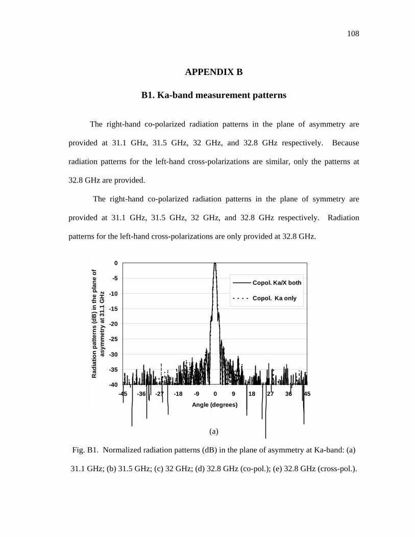
108
APPENDIX B
B1. Ka-band measurement patterns
The right-hand co-polarized radiation patterns in the plane of asymmetry are
provided at 31.1 GHz, 31.5 GHz, 32 GHz, and 32.8 GHz respectively. Because
radiation patterns for the left-hand cross-polarizations are similar, only the patterns at
32.8 GHz are provided.
The right-hand co-polarized radiation patterns in the plane of symmetry are
provided at 31.1 GHz, 31.5 GHz, 32 GHz, and 32.8 GHz respectively. Radiation
patterns for the left-hand cross-polarizations are only provided at 32.8 GHz.
-40
-35
-30
-25
-20
-15
-10
-5
0
-45 -36 -27 -18 -9 0 9 18 27 36 45
Angle (degrees)
Rad
iatio
n pa
ttern
s (d
B) i
n th
e pl
ane
of
asym
met
ry a
t 31.
1 G
Hz
Copol. Ka/X both
Copol. Ka only
(a)
Fig. B1. Normalized radiation patterns (dB) in the plane of asymmetry at Ka-band: (a)
31.1 GHz; (b) 31.5 GHz; (c) 32 GHz; (d) 32.8 GHz (co-pol.); (e) 32.8 GHz (cross-pol.).
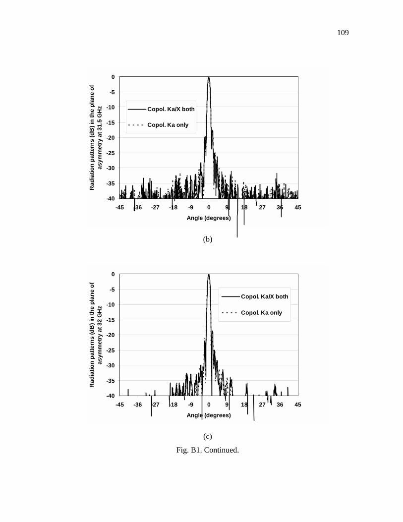
109
-40
-35
-30
-25
-20
-15
-10
-5
0
-45 -36 -27 -18 -9 0 9 18 27 36 45
Angle (degrees)
Rad
iatio
n pa
ttern
s (d
B) i
n th
e pl
ane
of
asym
met
ry a
t 31.
5 G
Hz Copol. Ka/X both
Copol. Ka only
(b)
-40
-35
-30
-25
-20
-15
-10
-5
0
-45 -36 -27 -18 -9 0 9 18 27 36 45
Angle (degrees)
Rad
iatio
n pa
ttern
s (d
B) i
n th
e pl
ane
of
asym
met
ry a
t 32
GH
z
Copol. Ka/X both
Copol. Ka only
(c)
Fig. B1. Continued.

110
-40
-35
-30
-25
-20
-15
-10
-5
0
-45 -36 -27 -18 -9 0 9 18 27 36 45
Angle (degrees)
Rad
iatio
n pa
ttern
s (d
B) i
n th
e pl
ane
of
asym
met
ry a
t 32.
8 G
Hz Copol. Ka/X both
Copol. Ka only
(d)
-50
-40
-30
-20
-10
0
-90 -75 -60 -45 -30 -15 0 15 30 45 60 75 90
Angle (degrees)
Rad
iatio
n pa
ttern
s (d
B) i
n th
e pl
ane
of
asym
met
ry a
t 32.
8 G
Hz Xpol. Ka/X both
Xpol. Ka only
(e)
Fig. B1. Continued.

111
-40
-35
-30
-25
-20
-15
-10
-5
0
-45 -36 -27 -18 -9 0 9 18 27 36 45
Angle (degrees)
Rad
iatio
n pa
ttern
s (d
B) i
n th
e pl
ane
of
sym
met
ry a
t 31.
1 G
Hz Copol. Ka/X both
Cpol. Ka only
(a)
-40
-35
-30
-25
-20
-15
-10
-5
0
-45 -36 -27 -18 -9 0 9 18 27 36 45
Angle (degrees)
Rad
iatio
n pa
ttern
s (d
B) i
n th
e pl
ane
of
sym
met
ry a
t 31.
5 G
Hz Copol. Ka/X both
Copol. Ka only
(b)
Fig. B2. Normalized radiation patterns (dB) in the plane of symmetry at Ka-band: (a)
31.1 GHz; (b) 31.5 GHz; (c) 32 GHz; (d) 32.8 GHz (co-pol.); (e) 32.8 GHz (cross-pol.).

112
-40
-35
-30
-25
-20
-15
-10
-5
0
-45 -36 -27 -18 -9 0 9 18 27 36 45
Angle (degrees)
Rad
iatio
n pa
ttern
s (d
B) i
n th
e pl
ane
of
sym
met
ry a
t 32
GH
z Copol. Ka/X both
Copol. Ka only
(c)
-40
-35
-30
-25
-20
-15
-10
-5
0
-45 -36 -27 -18 -9 0 9 18 27 36 45
Angle (degrees)
Rad
iatio
n pa
ttern
s (d
B) i
n th
e pl
ane
of
sym
met
ry a
t 32.
8 G
Hz Copol. Ka/X both
Copol. Ka only
(d)
Fig. B2. Continued.

113
-50
-40
-30
-20
-10
0
-90 -75 -60 -45 -30 -15 0 15 30 45 60 75 90
Angle (degrees)
Rad
iatio
n pa
ttern
s (d
B) i
n th
e pl
ane
of
sym
met
ry a
t 32.
8 G
Hz
Xpol. Ka/X both
Xpol. Ka only
(e)
Fig. B2. Continued.
B2. X-band measurement patterns
The right-hand co-polarized radiation patterns in the plane of asymmetry are
provided at 8.2 GHz, 8.4 GHz, 8.5 GHz, and 8.9 GHz respectively. Radiation patterns
for the left-hand cross-polarization are given only at 8.5 GHz.
Radiation patterns in the plane of symmetry are provided at 8.2 GHz, 8.4 GHz,
8.5 GHz, and 8.9 GHz respectively. Only the radiation patterns for the dual layer case
are measured in the plane of symmetry.
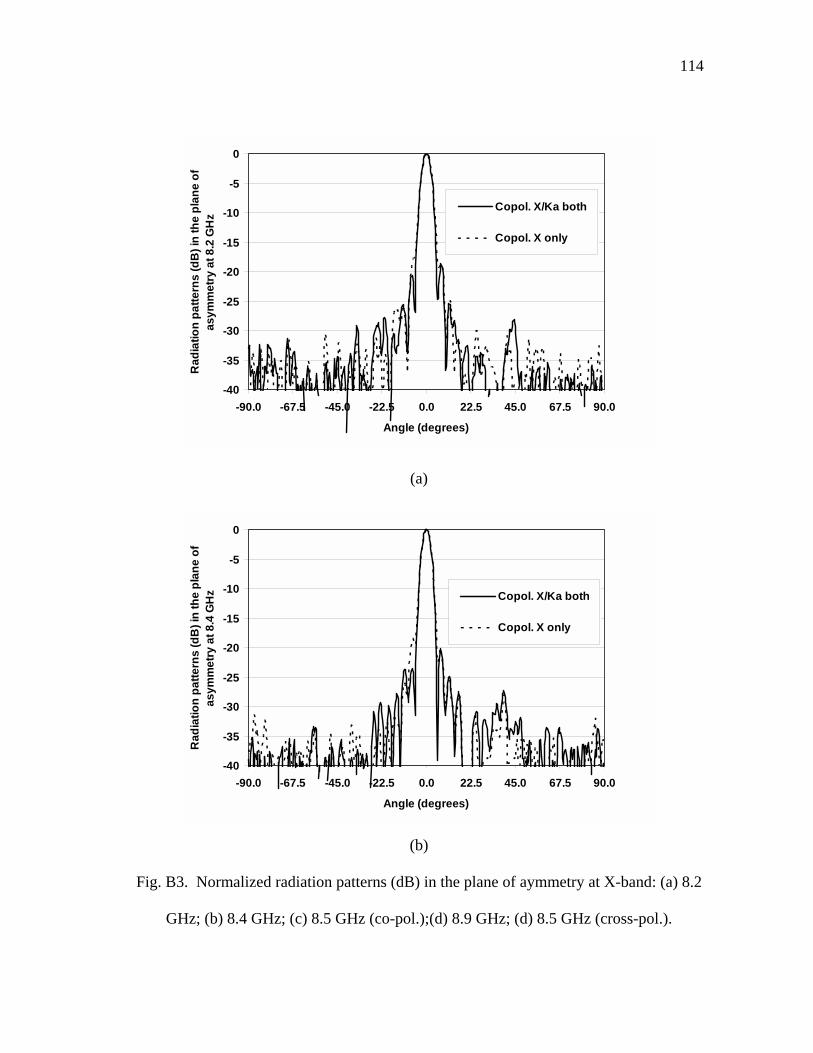
114
-40
-35
-30
-25
-20
-15
-10
-5
0
-90.0 -67.5 -45.0 -22.5 0.0 22.5 45.0 67.5 90.0
Angle (degrees)
Rad
iatio
n pa
ttern
s (d
B) i
n th
e pl
ane
of
asym
met
ry a
t 8.2
GH
zCopol. X/Ka both
Copol. X only
(a)
-40
-35
-30
-25
-20
-15
-10
-5
0
-90.0 -67.5 -45.0 -22.5 0.0 22.5 45.0 67.5 90.0
Angle (degrees)
Rad
iatio
n pa
ttern
s (d
B) i
n th
e pl
ane
of
asym
met
ry a
t 8.4
GH
z Copol. X/Ka both
Copol. X only
(b)
Fig. B3. Normalized radiation patterns (dB) in the plane of aymmetry at X-band: (a) 8.2
GHz; (b) 8.4 GHz; (c) 8.5 GHz (co-pol.);(d) 8.9 GHz; (d) 8.5 GHz (cross-pol.).

115
-40
-35
-30
-25
-20
-15
-10
-5
0
-90.0 -67.5 -45.0 -22.5 0.0 22.5 45.0 67.5 90.0
Angle (degrees)
Rad
iatio
n pa
ttern
s (d
B) i
n th
e pl
ane
of
asym
met
ry a
t 8.5
GH
z Copol. X/Ka both
Copol. X only
(c)
-40
-35
-30
-25
-20
-15
-10
-5
0
-90.0 -67.5 -45.0 -22.5 0.0 22.5 45.0 67.5 90.0
Angle (degrees)
Rad
iatio
n pa
ttern
s (d
B) i
n th
e pl
ane
of
asym
met
ry a
t 8.9
GH
z Copol. X/Ka both
Copol. X only
(d)
Fig. B3. Continued.

116
-60
-50
-40
-30
-20
-10
0
-90.0 -67.5 -45.0 -22.5 0.0 22.5 45.0 67.5 90.0
Angle (degrees)
Rad
iatio
n pa
ttern
s (d
B) i
n th
e pl
ane
of
asym
met
ry a
t 8.5
GH
z
Xpol. X/Ka both
Xpol. X only
(e)
Fig. B3. Continued.

117
-40
-35
-30
-25
-20
-15
-10
-5
0
-90.0 -67.5 -45.0 -22.5 0.0 22.5 45.0 67.5 90.0
Angle (degrees)
Rad
iatio
n pa
ttern
s (d
B) i
n th
e pl
ane
of
sym
met
ry a
t 8.2
GH
zCopol. X/Ka both
Xpol. X/Ka both
(a)
-40
-35
-30
-25
-20
-15
-10
-5
0
-90.0 -67.5 -45.0 -22.5 0.0 22.5 45.0 67.5 90.0
Angle (degrees)
Rad
iatio
n pa
ttern
s (d
B) i
n th
e pl
ane
of
sym
met
ry a
t 8.4
GH
z Copol. X/Ka both
Xpol. X/Ka both
(b)
Fig. B4. Normalized radiation patterns (dB) in the plane of symmetry at X-band: (a) 8.2
GHz; (b) 8.4 GHz; (c) 8.5 GHz; (d) 8.9 GHz.
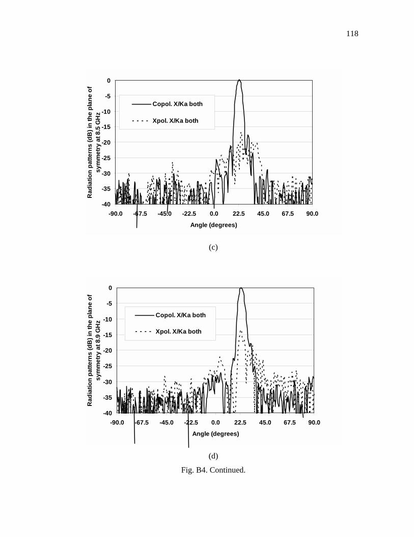
118
-40
-35
-30
-25
-20
-15
-10
-5
0
-90.0 -67.5 -45.0 -22.5 0.0 22.5 45.0 67.5 90.0
Angle (degrees)
Rad
iatio
n pa
ttern
s (d
B) i
n th
e pl
ane
of
sym
met
ry a
t 8.5
GH
zCopol. X/Ka both
Xpol. X/Ka both
(c)
-40
-35
-30
-25
-20
-15
-10
-5
0
-90.0 -67.5 -45.0 -22.5 0.0 22.5 45.0 67.5 90.0
Angle (degrees)
Rad
iatio
n pa
ttern
s (d
B) i
n th
e pl
ane
of
sym
met
ry a
t 8.9
GH
z
Copol. X/Ka both
Xpol. X/Ka both
(d)
Fig. B4. Continued.

119
APPENDIX C
C1. X-band measurement results
Normalized radiation patterns in the plane of asymmetry are provided at 8.2 GHz,
8.3 GHz, 8.5 GHz, and 8.6 GHz with the corresponding cross-polarization patterns.
Normalized radiation patterns in the offset plane (in the plane of symmetry) are provided
at 8 GHz, 8.3 GHz, 8.5 GHz, and 8.7 GHz respectively.
-40
-35
-30
-25
-20
-15
-10
-5
0
-90 -75 -60 -45 -30 -15 0 15 30 45 60 75 90
Angle (degrees)
Nor
mal
ized
radi
atio
n pa
ttens
(dB
) a
t 8.2
GH
z- a
sym
met
ric p
lane
Copol, X/Ka bothCopol, X onlyXpol, X/Ka bothXpol, X only
(a)
Fig. C1. Normalized radiation patterns (dB) in the asymmetric plane at X-band: (a) 8.2
GHz; (b) 8.3 GHz; (c) 8.5 GHz; (d) 8.6 GHz.
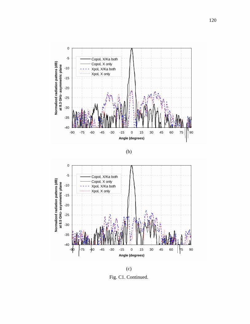
120
-40
-35
-30
-25
-20
-15
-10
-5
0
-90 -75 -60 -45 -30 -15 0 15 30 45 60 75 90
Angle (degrees)
Nor
mal
ized
radi
atio
n pa
ttens
(dB
) a
t 8.3
GH
z- a
sym
met
ric p
lane
Copol, X/Ka bothCopol, X onlyXpol, X/Ka bothXpol, X only
(b)
-40
-35
-30
-25
-20
-15
-10
-5
0
-90 -75 -60 -45 -30 -15 0 15 30 45 60 75 90
Angle (degrees)
Nor
mal
ized
radi
atio
n pa
ttens
(dB
) at
8.5
GH
z- a
sym
met
ric p
lane
Copol, X/Ka bothCopol, X onlyXpol, X/Ka bothXpol, X only
(c)
Fig. C1. Continued.
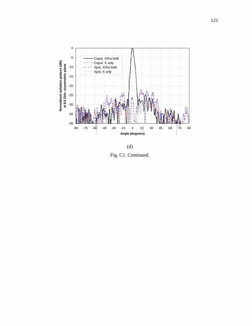
121
-40
-35
-30
-25
-20
-15
-10
-5
0
-90 -75 -60 -45 -30 -15 0 15 30 45 60 75 90
Angle (degrees)
Nor
mal
ized
radi
atio
n pa
ttens
(dB
) at
8.6
GH
z- a
sym
met
ric p
lane
Copol, X/Ka bothCopol, X onlyXpol, X/Ka bothXpol, X only
(d)
Fig. C1. Continued.

122
-40
-35
-30
-25
-20
-15
-10
-5
0
-90 -75 -60 -45 -30 -15 0 15 30 45 60 75 90
Angle (degrees)
Nor
mal
ized
radi
atio
n pa
ttens
(dB
) a
t 8.0
GH
z- o
ffset
pla
ne
Copol, X/Ka bothCopol, X onlyXpol, X/Ka bothXpol, X only
(a)
-40
-35
-30
-25
-20
-15
-10
-5
0
-90 -75 -60 -45 -30 -15 0 15 30 45 60 75 90
Angle (degrees)
Nor
mal
ized
radi
atio
n pa
ttens
(dB
) at
8.3
GH
z- o
ffset
pla
ne
Copol, X/Ka bothCopol, X onlyXpol, X/Ka bothXpol, X only
(b)
Fig. C2. Normalized radiation patterns (dB) in the offset plane at X-band: (a) 8.0 GHz;
(b) 8.3 GHz; (c) 8.5 GHz; (d) 8.7 GHz.

123
-40
-35
-30
-25
-20
-15
-10
-5
0
-90 -75 -60 -45 -30 -15 0 15 30 45 60 75 90
Angle (degrees)
Nor
mal
ized
radi
atio
n pa
ttens
(dB
) a
t 8.5
GH
z- o
ffset
pla
neCopol, X/Ka bothCopol, X onlyXpol, X/Ka bothXpol, X only
(c)
-40
-35
-30
-25
-20
-15
-10
-5
0
-90 -75 -60 -45 -30 -15 0 15 30 45 60 75 90
Angle (degrees)
Nor
mal
ized
radi
atio
n pa
ttens
(dB
) at
8.7
GH
z- o
ffset
pla
ne
Copol, X/Ka bothCopol, X onlyXpol, X/Ka bothXpol, X only
(d)
Fig. C2. Continued.

124
C2. Ka-band measurement results
Normalized radiation patterns in the plane of asymmetry are provided at 31 GHz,
31.4 GHz, 32 GHz, 32.6 GHz and 33 GHz with the corresponding cross-polarization
patterns. Normalized radiation patterns in the offset plane (in the plane of symmetry) are
provided at 31 GHz, 31.6 GHz, 32 GHz, 32.4 GHz and 33 GHz respectively.
-40
-35
-30
-25
-20
-15
-10
-5
0
-30 -25 -20 -15 -10 -5 0 5 10 15 20 25 30
Angle (degrees)
Nor
mal
ized
radi
atio
n pa
ttern
s (d
B)
at 3
1 G
Hz-
asy
mm
etric
pla
ne Copol, Ka/X both
Copol, Ka only
Xpol, Ka/X both
Xpol, Ka only
(a)
Fig. C3. Normalized radiation patterns (dB) in the asymmetric plane at Ka-band: (a) 31
GHz; (b) 31.4 GHz; (c) 32 GHz; (d) 32.6 GHz; (e) 33 GHz.

125
-40
-35
-30
-25
-20
-15
-10
-5
0
-30 -25 -20 -15 -10 -5 0 5 10 15 20 25 30
Angle (degrees)
Nor
mal
ized
radi
atio
n pa
ttern
s (d
B)
at 3
1.4
GH
z- a
sym
met
ric p
lane Copol, Ka/X both
Copol, Ka only
Xpol, Ka/X both
Xpol, Ka only
(b)
-40
-35
-30
-25
-20
-15
-10
-5
0
-30 -25 -20 -15 -10 -5 0 5 10 15 20 25 30
Angle (degrees)
Nor
mal
ized
radi
atio
n pa
ttern
s (d
B)
at 3
2 G
Hz-
asy
mm
etric
pla
ne Copol, Ka/X both
Copol, Ka only
Xpol, Ka/X both
Xpol, Ka only
(c)
Fig. C3. Continued.

126
-40
-35
-30
-25
-20
-15
-10
-5
0
-30 -25 -20 -15 -10 -5 0 5 10 15 20 25 30
Angle (degrees)
Nor
mal
ized
radi
atio
n pa
ttern
s (d
B)
at 3
2.6
GH
z- a
sym
met
ric p
lane Copol, Ka/X both
Copol, Ka only
Xpol, Ka/X both
Xpol, Ka only
(d)
-40
-35
-30
-25
-20
-15
-10
-5
0
-30 -25 -20 -15 -10 -5 0 5 10 15 20 25 30
Angle (degrees)
Nor
mal
ized
radi
atio
n pa
ttern
s (d
B)
at 3
3 G
Hz-
asy
mm
etric
pla
ne Copol, Ka/X both
Copol, Ka only
Xpol, Ka/X both
Xpol, Ka only
(e)
Fig. C3. Continued.

127
-40
-35
-30
-25
-20
-15
-10
-5
0
-45 -30 -15 0 15 30 45
Angle (degrees)
Nor
mal
ized
radi
atio
n pa
ttern
s (d
B)
at 3
1 G
Hz-
offs
et p
lane
Copol, Ka/X bothCopol, Ka onlyXpol, Ka/X bothXpol, Ka only
(a)
-40
-35
-30
-25
-20
-15
-10
-5
0
-45 -30 -15 0 15 30 45
Angle (degrees)
Nor
mal
ized
radi
atio
n pa
ttern
s (d
B)
at 3
1.6
GH
z- o
ffset
pla
ne
Copol, Ka/X bothCopol, Ka onlyXpol, Ka/X bothXpol, Ka only
(b)
Fig. C4. Normalized radiation patterns (dB) in the offset plane at Ka-band: (a) 31 GHz;
(b) 31.6 GHz; (c) 32 GHz; (d) 32.4 GHz; (e) 33 GHz.

128
-40
-35
-30
-25
-20
-15
-10
-5
0
-45 -30 -15 0 15 30 45
Angle (degrees)
Nor
mal
ized
radi
atio
n pa
ttern
s (d
B)
at 3
2 G
Hz-
offs
et p
lane
Copol, Ka/X bothCopol, Ka onlyXpol, Ka/X bothXpol, Ka only
(c)
-40
-35
-30
-25
-20
-15
-10
-5
0
-45 -30 -15 0 15 30 45
Angle (degrees)
Nor
mal
ized
radi
atio
n pa
ttern
s (d
B)
at 3
2.4
GH
z- o
ffset
pla
ne
Copol, Ka/X bothCopol, Ka onlyXpol, Ka/X bothXpol, Ka only
(d)
Fig. C4. Continued.

129
-40
-35
-30
-25
-20
-15
-10
-5
0
-45 -30 -15 0 15 30 45
Angle (degrees)
Nor
mal
ized
radi
atio
n pa
ttern
s (d
B)
at 3
3 G
Hz-
offs
et p
lane
Copol, Ka/X bothCopol, Ka onlyXpol, Ka/X bothXpol, Ka only
(e)
Fig. C4. Continued.

130
VITA
Chul Min Han was born in Jun-Ju, Republic of Korea on Jan. 18, 1972. He
received his B.S. in electronics engineering from Korea University in Aug. 1997. In
2000, he started his Ph.D. degree in electrical engineering at Texas A&M University,
College Station, Texas and was guided by Dr. Kai Chang in the Electromagnetics and
Microwave Laboratory. He is a grateful recipient of the Ebens-berger Gaduate
Fellowship in the Department of Electrical Engineering in 2005. During the summer
months of 2001, he was employed by Mimix Broadband Inc. in Houston as an
engineering intern working on active biasing circuits for microwave monolithic circuits.
His graduate research projects have been supported by grants from the NASA Jet
Propulsion Laboratory. He can be reached through Professor Kai Chang, Department of
Electrical Engineering, Texas A&M University, College Station, TX 77843-3128.