dual asynchronous receiver/transmitter (duart) · dual asynchronous receiver/transmitter (duart)...
TRANSCRIPT
SCC2692Dual asynchronous receiver/transmitter(DUART)
Product specificationSupersedes data of 1998 Feb 19IC19 Data Handbook
1998 Sep 04
INTEGRATED CIRCUITS

Philips Semiconductors Product specification
SCC2692Dual asynchronous receiver/transmitter (DUART)
21998 Sep 04 853–0895 19971
DESCRIPTIONThe Philips Semiconductors SCC2692 Dual UniversalAsynchronous Receiver/Transmitter (DUART) which is compatiblewith the SCN2681. It is a single-chip CMOS-LSI communicationsdevice that provides two full-duplex asynchronousreceiver/transmitter channels in a single package. It interfacesdirectly with microprocessors and may be used in a polled orinterrupt driven system.
The operating mode and data format of each channel can beprogrammed independently. Additionally, each receiver andtransmitter can select its operating speed as one of eighteen fixedbaud rates, a 16X clock derived from a programmable counter/timer,or an external 1X or 16X clock. The baud rate generator andcounter/timer can operate directly from a crystal or from externalclock inputs. The ability to independently program the operatingspeed of the receiver and transmitter make the DUART particularlyattractive for dual-speed channel applications such as clusteredterminal systems.
Each receiver is quadruply buffered to minimize the potential ofreceiver over-run or to reduce interrupt overhead in interrupt drivensystems. In addition, a flow control capability is provided to disable aremote DUART transmitter when the receiver buffer is full.
Also provided on the SCC2692 are a multipurpose 7-bit input portand a multipurpose 8-bit output port. These can be used as generalpurpose I/O ports or can be assigned specific functions (such asclock inputs or status/interrupt outputs) under program control.
FEATURES• Dual full-duplex asynchronous receiver/transmitters
• Quadruple buffered receiver data register
• Programmable data format
– 5 to 8 data bits plus parity
– Odd, even, no parity or force parity
– 1, 1.5 or 2 stop bits programmable in 1/16-bit increments
• 16-bit programmable Counter/Timer
• Programmable baud rate for each receiver and transmitterselectable from:
– 22 fixed rates: 50 to 115.2k baud
– Non-standard rates to 115.2Kb
– Non-standard user-defined rate derived from programmablecounter/timer
– External 1X or 16X clock
• Parity, framing, and overrun error detection
• False start bit detection
• Line break detection and generation
• Programmable channel mode
– Normal (full-duplex)
– Automatic echo
– Local loopback
– Remote loopback
– Multidrop mode (also called ‘wake-up’ or ‘9-bit’)
• Multi-function 7-bit input port
– Can serve as clock or control inputs
– Change of state detection on four inputs
– Inputs have typically >100k pull-up resistors
• Multi-function 8-bit output port
– Individual bit set/reset capability
– Outputs can be programmed to be status/interrupt signals
• Versatile interrupt system
– Single interrupt output with eight maskable interruptingconditions
– Output port can be configured to provide a total of up to sixseparate wire-ORable interrupt outputs
• Maximum data transfer rates: 1X – 1MB/sec, 16X – 125kB/sec
• Automatic wake-up mode for multidrop applications
• Start-end break interrupt/status
• Detects break which originates in the middle of a character
• On-chip crystal oscillator
• Power down mode
• Receiver timeout mode
• Commercial and industrial temperature range versions
• TTL compatible
• Single +5V power supply
ORDERING INFORMATIONCOMMERCIAL INDUSTRIAL
DESCRIPTION VCC = +5V +10%,TA = 0 to +70°C
VCC = +5V +10%,TA = -40 to +85°C
DWG #
40-Pin Plastic Dual In-Line Package (DIP)1 SCC2692AC1N40 SCC2692AE1N40 SOT129-1
28-Pin Plastic Dual In-Line Package (DIP)1 SCC2692AC1N28 SCC2692AE1N28 SOT117-1
44-Pin Plastic Leaded Chip Carrier (PLCC) Package SCC2692AC1A44 SCC2692AE1A44 SOT187-2
44–Pin Plastic Quad Flat Pack (PQFP) SCC2692AC1B44 SCC2692AE1B44 SOT307–2
NOTE:1. For availability, please contact factory.
Philips Semiconductors Product specification
SCC2692Dual asynchronous receiver/transmitter (DUART)
1998 Sep 04 3
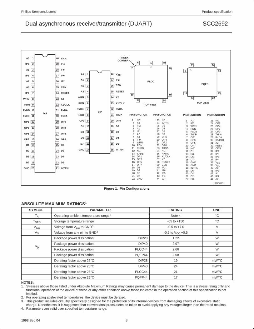
PIN/FUNCTION PIN/FUNCTION 1 NC 23 NC 2 A0 24 INTRN 3 IP3 25 D6 4 A1 26 D4 5 IP1 27 D2 6 A2 28 D0 7 A3 29 OP6 8 IP0 30 OP4 9 WRN 31 OP210 RDN 32 OP011 RXDB 33 TXDA12 NC 34 NC13 TXDB 35 RXDA14 OP1 36 X1/CLK15 OP3 37 X216 OP5 38 RESET17 OP7 39 CEN18 D1 40 IP219 D3 41 IP620 D5 42 IP521 D7 43 IP422 GND 44 VCC
24
23
22
2120
19
18
17
16
15
28
27
12
10
11
9
8
7
6
5
4
3
2
1
14
13
26
25
29
30
31
32
33
34
35
36
37
38
39
40
DIP
VCC
IP4
IP5
IP6
IP2
CEN
RESET
X2
X1/CLK
RxDA
TxDA
OP0
OP2
OP4
OP6
D0
D2
D4
D6
INTRN
A0
IP3
A1
IP1
A2
A3
IP0
WRN
RDN
RxDB
TxDB
OP1
OP3
OP5
OP7
D1
D3
D5
D7
GND
24
23
22
21
20
19
18
17
16
15
28
27
12
10
11
9
8
7
6
5
4
3
2
1
14
13
26
25
VCC
IP2
CEN
RESET
X2
X1/CLK
RxDA
TxDA
OP0
D0
D2
D4
D6
INTRNGND
D7
D5
D3
D1
OP1
TxDB
RxDB
RDN
WRN
A3
A2
A1
A0
DIP
1
39
17
28
40
29
18
7
PLCC
6
INDEXCORNER
SD00131
PIN/FUNCTION PIN/FUNCTION 1 A3 23 N/C 2 IP0 24 OP6 3 WRN 25 OP4 4 RDN 26 OP2 5 RxDB 27 OP0 6 TxDB 28 TxDA 7 OP1 29 RxDA 8 OP3 30 X1/CLK 9 OP5 31 X210 OP7 32 RESET11 N/C 33 CEN12 D1 34 IP213 D3 35 IP614 D5 36 IP515 D7 37 IP416 GND 38 VCC17 GND 39 VCC18 INTRN 40 A019 D6 41 IP320 D4 42 A121 D2 43 IP122 D0 44 A2
TOP VIEW
33
11
22
34
23
12
1
PQFP
44
TOP VIEW
Figure 1. Pin Configurations
ABSOLUTE MAXIMUM RATINGS 1
SYMBOL PARAMETER RATING UNIT
TA Operating ambient temperature range2 Note 4 °C
TSTG Storage temperature range -65 to +150 °C
VCC Voltage from VCC to GND3 -0.5 to +7.0 V
VS Voltage from any pin to GND3 -0.5 to VCC +0.5 V
Package power dissipation DIP28 1.22 W
PPackage power dissipation DIP40 2.97 W
PDPackage power dissipation PLCC44 2.66 W
Package power dissipation PQFP44 2.08 W
Derating factor above 25°C DIP28 19 mW/°C
Derating factor above 25°C DIP40 24 mW/°C
Derating factor above 25°C PLCC44 21 mW/°C
Derating factor above 25°C PQFP44 17 mW/°CNOTES:1. Stresses above those listed under Absolute Maximum Ratings may cause permanent damage to the device. This is a stress rating only and
functional operation of the device at these or any other condition above those indicated in the operation section of this specification is notimplied.
2. For operating at elevated temperatures, the device must be derated.3. This product includes circuitry specifically designed for the protection of its internal devices from damaging effects of excessive static
charge. Nonetheless, it is suggested that conventional precautions be taken to avoid applying any voltages larger than the rated maxima.4. Parameters are valid over specified temperature range.
Philips Semiconductors Product specification
SCC2692Dual asynchronous receiver/transmitter (DUART)
1998 Sep 04 4
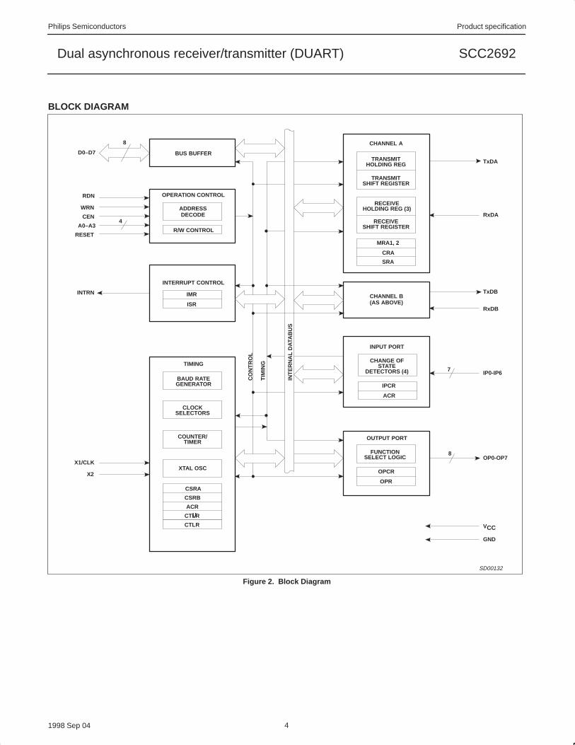
BLOCK DIAGRAM
8
D0–D7
RDN
WRN
CEN
A0–A3
RESET
INTRN
X1/CLK
X2
4
BUS BUFFER
OPERATION CONTROL
ADDRESSDECODE
R/W CONTROL
INTERRUPT CONTROL
IMR
ISR
TIMING
BAUD RATEGENERATOR
CLOCKSELECTORS
COUNTER/TIMER
XTAL OSC
CSRA
CSRB
ACR
CTLR
CHANNEL A
TRANSMITHOLDING REG
TRANSMITSHIFT REGISTER
RECEIVEHOLDING REG (3)
RECEIVESHIFT REGISTER
MRA1, 2
CRA
SRA
INPUT PORT
CHANGE OFSTATE
DETECTORS (4)
OUTPUT PORT
FUNCTIONSELECT LOGIC
OPCR
TxDA
RxDA
IP0-IP6
OP0-OP7
VCC
GND
CO
NT
RO
L
TIM
ING
INT
ER
NA
L D
ATA
BU
SCHANNEL B(AS ABOVE)
IPCR
ACR
OPR
CTLR
U
RxDB
TxDB
8
7
SD00132
Figure 2. Block Diagram
Philips Semiconductors Product specification
SCC2692Dual asynchronous receiver/transmitter (DUART)
1998 Sep 04 5
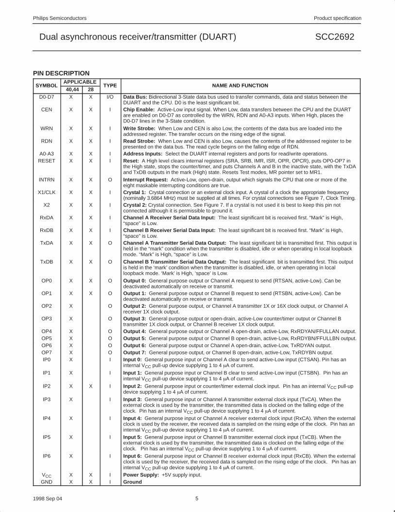
PIN DESCRIPTION
SYMBOLAPPLICABLE
TYPE NAME AND FUNCTIONSYMBOL 40,44 28
TYPE NAME AND FUNCTION
D0-D7 X X I/O Data Bus: Bidirectional 3-State data bus used to transfer commands, data and status between theDUART and the CPU. D0 is the least significant bit.
CEN X X I Chip Enable: Active-Low input signal. When Low, data transfers between the CPU and the DUARTare enabled on D0-D7 as controlled by the WRN, RDN and A0-A3 inputs. When High, places theD0-D7 lines in the 3-State condition.
WRN X X I Write Strobe: When Low and CEN is also Low, the contents of the data bus are loaded into theaddressed register. The transfer occurs on the rising edge of the signal.
RDN X X I Read Strobe: When Low and CEN is also Low, causes the contents of the addressed register to bepresented on the data bus. The read cycle begins on the falling edge of RDN.
A0-A3 X X I Address Inputs: Select the DUART internal registers and ports for read/write operations.RESET X X I Reset: A High level clears internal registers (SRA, SRB, IMR, ISR, OPR, OPCR), puts OP0-OP7 in
the High state, stops the counter/timer, and puts Channels A and B in the inactive state, with the TxDAand TxDB outputs in the mark (High) state. Resets Test modes, MR pointer set to MR1.
INTRN X X O Interrupt Request: Active-Low, open-drain, output which signals the CPU that one or more of theeight maskable interrupting conditions are true.
X1/CLK X X I Crystal 1: Crystal connection or an external clock input. A crystal of a clock the appropriate frequency(nominally 3.6864 MHz) must be supplied at all times. For crystal connections see Figure 7, Clock Timing.
X2 X X I Crystal 2: Crystal connection. See Figure 7. If a crystal is not used it is best to keep this pin notconnected although it is permissible to ground it.
RxDA X X I Channel A Receiver Serial Data Input: The least significant bit is received first. “Mark” is High,“space” is Low.
RxDB X X I Channel B Receiver Serial Data Input: The least significant bit is received first. “Mark” is High,“space” is Low.
TxDA X X O Channel A Transmitter Serial Data Output: The least significant bit is transmitted first. This output isheld in the “mark” condition when the transmitter is disabled, idle or when operating in local loopbackmode. “Mark” is High, “space” is Low.
TxDB X X O Channel B Transmitter Serial Data Output: The least significant bit is transmitted first. This outputis held in the ‘mark’ condition when the transmitter is disabled, idle, or when operating in localloopback mode. ‘Mark’ is High, ‘space’ is Low.
OP0 X X O Output 0: General purpose output or Channel A request to send (RTSAN, active-Low). Can bedeactivated automatically on receive or transmit.
OP1 X X O Output 1: General purpose output or Channel B request to send (RTSBN, active-Low). Can bedeactivated automatically on receive or transmit.
OP2 X O Output 2: General purpose output, or Channel A transmitter 1X or 16X clock output, or Channel Areceiver 1X clock output.
OP3 X O Output 3: General purpose output or open-drain, active-Low counter/timer output or Channel Btransmitter 1X clock output, or Channel B receiver 1X clock output.
OP4 X O Output 4: General purpose output or Channel A open-drain, active-Low, RxRDYAN/FFULLAN output.OP5 X O Output 5: General purpose output or Channel B open-drain, active-Low, RxRDYBN/FFULLBN output.OP6 X O Output 6: General purpose output or Channel A open-drain, active-Low, TxRDYAN output.OP7 X O Output 7: General purpose output, or Channel B open-drain, active-Low, TxRDYBN output.IP0 X I Input 0: General purpose input or Channel A clear to send active-Low input (CTSAN). Pin has an
internal VCC pull-up device supplying 1 to 4 A of current.
IP1 X I Input 1: General purpose input or Channel B clear to send active-Low input (CTSBN). Pin has aninternal VCC pull-up device supplying 1 to 4 A of current.
IP2 X X I Input 2: General purpose input or counter/timer external clock input. Pin has an internal VCC pull-updevice supplying 1 to 4 A of current.
IP3 X I Input 3: General purpose input or Channel A transmitter external clock input (TxCA). When theexternal clock is used by the transmitter, the transmitted data is clocked on the falling edge of theclock. Pin has an internal VCC pull-up device supplying 1 to 4 A of current.
IP4 X I Input 4: General purpose input or Channel A receiver external clock input (RxCA). When the externalclock is used by the receiver, the received data is sampled on the rising edge of the clock. Pin has aninternal VCC pull-up device supplying 1 to 4 A of current.
IP5 X I Input 5: General purpose input or Channel B transmitter external clock input (TxCB). When theexternal clock is used by the transmitter, the transmitted data is clocked on the falling edge of theclock. Pin has an internal VCC pull-up device supplying 1 to 4 A of current.
IP6 X I Input 6: General purpose input or Channel B receiver external clock input (RxCB). When the externalclock is used by the receiver, the received data is sampled on the rising edge of the clock. Pin has aninternal VCC pull-up device supplying 1 to 4 A of current.
VCC X X I Power Supply: +5V supply input.GND X X I Ground
Philips Semiconductors Product specification
SCC2692Dual asynchronous receiver/transmitter (DUART)
1998 Sep 04 6
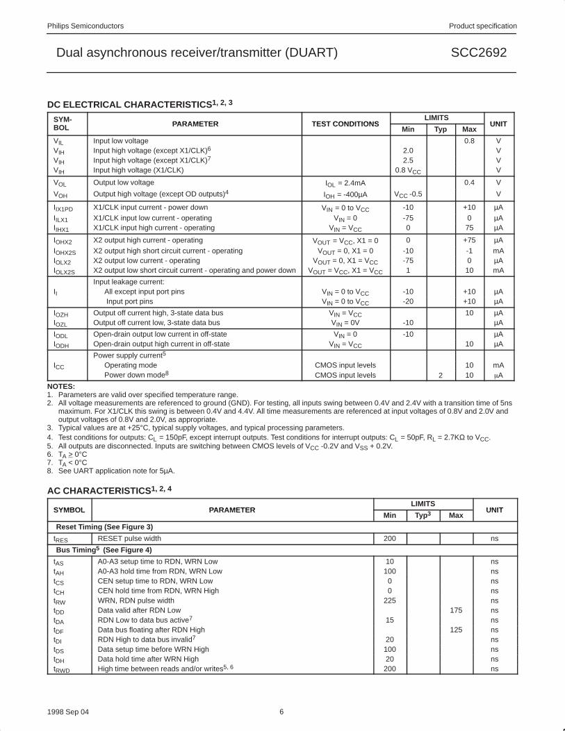
DC ELECTRICAL CHARACTERISTICS 1, 2, 3
SYM-PARAMETER TEST CONDITIONS
LIMITSUNITBOL PARAMETER TEST CONDITIONS
Min Typ MaxUNIT
VIL Input low voltage 0.8 VVIH Input high voltage (except X1/CLK)6 2.0 VVIH Input high voltage (except X1/CLK)7 2.5 VVIH Input high voltage (X1/CLK) 0.8 VCC V
VOL Output low voltage IOL = 2.4mA 0.4 V
VOH Output high voltage (except OD outputs)4 IOH = -400µA VCC -0.5 V
IIX1PD X1/CLK input current - power down VIN = 0 to VCC -10 +10 µA
IILX1 X1/CLK input low current - operating VIN = 0 -75 0 µAIIHX1 X1/CLK input high current - operating VIN = VCC 0 75 µA
IOHX2 X2 output high current - operating VOUT = VCC, X1 = 0 0 +75 µA
IOHX2S X2 output high short circuit current - operating VOUT = 0, X1 = 0 -10 -1 mAIOLX2 X2 output low current - operating VOUT = 0, X1 = VCC -75 0 µAIOLX2S X2 output low short circuit current - operating and power down VOUT = VCC, X1 = VCC 1 10 mA
Input leakage current:II All except input port pins VIN = 0 to VCC -10 +10 µA
Input port pins VIN = 0 to VCC -20 +10 µA
IOZH Output off current high, 3-state data bus VIN = VCC 10 µAIOZL Output off current low, 3-state data bus VIN = 0V -10 µA
IODL Open-drain output low current in off-state VIN = 0 -10 µAIODH Open-drain output high current in off-state VIN = VCC 10 µA
Power supply current5
ICC Operating mode CMOS input levels 10 mAPower down mode8 CMOS input levels 2 10 A
NOTES:1. Parameters are valid over specified temperature range.2. All voltage measurements are referenced to ground (GND). For testing, all inputs swing between 0.4V and 2.4V with a transition time of 5ns
maximum. For X1/CLK this swing is between 0.4V and 4.4V. All time measurements are referenced at input voltages of 0.8V and 2.0V andoutput voltages of 0.8V and 2.0V, as appropriate.
3. Typical values are at +25°C, typical supply voltages, and typical processing parameters.4. Test conditions for outputs: CL = 150pF, except interrupt outputs. Test conditions for interrupt outputs: CL = 50pF, RL = 2.7KΩ to VCC.5. All outputs are disconnected. Inputs are switching between CMOS levels of VCC -0.2V and VSS + 0.2V.6. TA > 0°C7. TA < 0°C8. See UART application note for 5µA.
AC CHARACTERISTICS 1, 2, 4
SYMBOL PARAMETERLIMITS
UNITSYMBOL PARAMETERMin Typ3 Max
UNIT
Reset Timing (See Figure 3)
tRES RESET pulse width 200 ns
Bus Timing 5 (See Figure 4)
tAS A0-A3 setup time to RDN, WRN Low 10 nstAH A0-A3 hold time from RDN, WRN Low 100 nstCS CEN setup time to RDN, WRN Low 0 nstCH CEN hold time from RDN, WRN High 0 nstRW WRN, RDN pulse width 225 nstDD Data valid after RDN Low 175 nstDA RDN Low to data bus active7 15 nstDF Data bus floating after RDN High 125 nstDI RDN High to data bus invalid7 20 nstDS Data setup time before WRN High 100 nstDH Data hold time after WRN High 20 nstRWD High time between reads and/or writes5, 6 200 ns
Philips Semiconductors Product specification
SCC2692Dual asynchronous receiver/transmitter (DUART)
1998 Sep 04 7
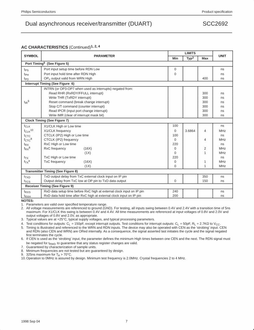
AC CHARACTERISTICS (Continued)1, 2, 4
SYMBOL PARAMETERLIMITS
UNITSYMBOL PARAMETERMin Typ3 Max
UNIT
Port Timing 5 (See Figure 5)
tPS Port input setup time before RDN Low 0 ns
tPH Port input hold time after RDN High 0 nstPD OPn output valid from WRN High 400 ns
Interrupt Timing (See Figure 6)
9
INTRN (or OP3-OP7 when used as interrupts) negated from:
9
Read RHR (RxRDY/FFULL interrupt) 300 ns
9Write THR (TxRDY interrupt) 300 ns
tIR9 Reset command (break change interrupt) 300 nsStop C/T command (counter interrupt) 300 nsRead IPCR (input port change interrupt) 300 nsWrite IMR (clear of interrupt mask bit) 300 ns
Clock Timing (See Figure 7)
tCLK X1/CLK High or Low time 100 ns
fCLK10 X1/CLK frequency 0 3.6864 4 MHz
tCTC CTCLK (IP2) High or Low time 100 nsfCTC
8 CTCLK (IP2) frequency 0 4 MHztRX RxC High or Low time 220 nsfRX
8 RxC frequency (16X) 0 2 MHz (1X) 0 1 MHz
tTX TxC High or Low time 220 nsfTX
8 TxC frequency (16X) 0 1 MHz (1X) 0 1 MHz
Transmitter Timing (See Figure 8)
tTXD TxD output delay from TxC external clock input on IP pin 350 nstTCS Output delay from TxC low at OP pin to TxD data output 0 150 ns
Receiver Timing (See Figure 9)
tRXS RxD data setup time before RxC high at external clock input on IP pin 240 nstRXH RxD data hold time after RxC high at external clock input on IP pin 200 ns
NOTES:1. Parameters are valid over specified temperature range.2. All voltage measurements are referenced to ground (GND). For testing, all inputs swing between 0.4V and 2.4V with a transition time of 5ns
maximum. For X1/CLK this swing is between 0.4V and 4.4V. All time measurements are referenced at input voltages of 0.8V and 2.0V andoutput voltages of 0.8V and 2.0V, as appropriate.
3. Typical values are at +25°C, typical supply voltages, and typical processing parameters.4. Test conditions for outputs: CL = 150pF, except interrupt outputs. Test conditions for interrupt outputs: CL = 50pF, RL = 2.7KΩ to VCC.5. Timing is illustrated and referenced to the WRN and RDN inputs. The device may also be operated with CEN as the ‘strobing’ input. CEN
and RDN (also CEN and WRN) are ORed internally. As a consequence, the signal asserted last initiates the cycle and the signal negatedfirst terminates the cycle.
6. If CEN is used as the ‘strobing’ input, the parameter defines the minimum High times between one CEN and the next. The RDN signal mustbe negated for tRWD to guarantee that any status register changes are valid.
7. Guaranteed by characterization of sample units.8. Minimum frequencies are not tested but are guaranteed by design.9. 325ns maximum for TA > 70°C.10. Operation to 0MHz is assured by design. Minimum test frequency is 2.0MHz. Crystal frequencies 2 to 4 MHz.
Philips Semiconductors Product specification
SCC2692Dual asynchronous receiver/transmitter (DUART)
1998 Sep 04 8
BLOCK DIAGRAMThe SCC2692 DUART consists of the following eight major sections:data bus buffer, operation control, interrupt control, timing,communications Channels A and B, input port and output port. Referto the Block Diagram.
Data Bus BufferThe data bus buffer provides the interface between the external andinternal data buses. It is controlled by the operation control block toallow read and write operations to take place between the controllingCPU and the DUART.
Operation ControlThe operation control logic receives operation commands from theCPU and generates appropriate signals to internal sections tocontrol device operation. It contains address decoding and read andwrite circuits to permit communications with the microprocessor viathe data bus buffer.
Interrupt ControlA single active-Low interrupt output (INTRN) is provided which isactivated upon the occurrence of any of eight internal events.Associated with the interrupt system are the Interrupt Mask Register(IMR) and the Interrupt Status Register (ISR). The IMR can beprogrammed to select only certain conditions to cause INTRN to beasserted. The ISR can be read by the CPU to determine all currentlyactive interrupting conditions.
Outputs OP3-OP7 can be programmed to provide discrete interruptoutputs for the transmitter, receivers, and counter/timer.
TIMING CIRCUITS
Crystal ClockThe timing block consists of a crystal oscillator, a baud rategenerator, a programmable 16-bit counter/timer, and four clockselectors. The crystal oscillator operates directly from a crystalconnected across the X1/CLK and X2 inputs. If an external clock ofthe appropriate frequency is available, it may be connected toX1/CLK. The clock serves as the basic timing reference for the BaudRate Generator (BRG), the counter/timer, and other internal circuits.A clock signal within the limits specified in the specifications sectionof this data sheet must always be supplied to the DUART.
If an external clock is used instead of a crystal, X1 should be drivenusing a configuration similar to the one in Figure 7.
BRGThe baud rate generator operates from the oscillator or externalclock input and is capable of generating 23 commonly used datacommunications baud rates ranging from 50 to 130.4K baud. A3.6864MHz crystal or external clock must be used to get thestandard baud rate. The clock outputs from the BRG are at 16X theactual baud rate. The counter/timer can be used as a timer toproduce a 16X clock for any other baud rate by counting down thecrystal clock or an external clock. The four clock selectors allow theindependent selection, for each receiver and transmitter, of any ofthese baud rates or external timing signal.
Counter/Timer (C/T)The counter timer is a 16 bit programmable divider that operatesone of three modes: Counter, Timer or Time Out mode. In all threemodes it uses the 16-bit value loaded to the CTUR and CTLRregisters. (Counter timer upper and lower preset registers).
• In the timer mode it generates a square wave.
• In the counter mode it generates a time delay.
• In the time out mode it monitors the receiver data flow and signalsdata flow has paused. In the time out mode the receiver controlsthe starting/stopping of the C/T.
The counter operates as a down counter and sets its output bit inthe ISR (Interrupt Status Register) each time it passes through 0.The output of the counter/timer may be seen on one of the OP pinsor as an Rx or Tx clock.
The Timer/Counter is controlled with six (6) “commands”; Start C/T,Stop C/T, write C/T, preset registers, read C/T value, set or resettime out mode.
Please see the detail of the commands under the Counter/Timerregister descriptions.
Communications Channels A and BEach communications channel of the SCC2692 comprises afull-duplex asynchronous receiver/transmitter (UART). The operatingfrequency for each receiver and transmitter can be selectedindependently from the baud rate generator, the counter/timer, orfrom an external input.
The transmitter accepts parallel data from the CPU, converts it to aserial bit stream, inserts the appropriate start, stop, and optionalparity bits and outputs a composite serial stream of data on the TxDoutput pin. The receiver accepts serial data on the RxD pin,converts this serial input to parallel format, checks for start bit, stopbit, parity bit (if any), or break condition and sends an assembledcharacter to the CPU.
Input PortThe inputs to this unlatched 7-bit port can be read by the CPU byperforming a read operation at address H’D’. A High input results ina logic 1 while a Low input results in a logic 0. D7 will always readas a logic 1. The pins of this port can also serve as auxiliary inputsto certain portions of the DUART logic.
Four change-of-state detectors are provided which are associatedwith inputs IP3, IP2, IP1 and IP0. A High-to-Low or Low-to-Hightransition of these inputs, lasting longer than 25 - 50µs, will set thecorresponding bit in the input port change register. The bits arecleared when the register is read by the CPU. Any change-of-statecan also be programmed to generate an interrupt to the CPU.
The input port pulse detection circuitry uses a 38.4KHz samplingclock derived from one of the baud rate generator taps. This resultsin a sampling period of slightly more than 25µs (this assumes thatthe clock input is 3.6864MHz). The detection circuitry, in order toguarantee that a true change in level has occurred, requires twosuccessive samples at the new logic level be observed. As aconsequence, the minimum duration of the signal change is 25µs ifthe transition occurs “coincident with the first sample pulse”. The50µs time refers to the situation in which the change-of-state is “justmissed” and the first change-of-state is not detected until 25µs later.All the IP pins have a small pull-up device that will source 1 to 4 Aof current from VCC. These pins do not require pull-up devices orVCC connections if they are not used.
Output PortThe output port pins may be controlled by the OPR, OPCR, MR andCR registers. Via appropriate programming they may be just anotherparallel port to external circuits, or they may represent many internal
Philips Semiconductors Product specification
SCC2692Dual asynchronous receiver/transmitter (DUART)
1998 Sep 04 9
conditions of the UART. When this 8-bit port is used as a generalpurpose output, the pins so defined will assume the compliment ofthe associated bit in the Output Port Register (OPR). OPR(n) = 1results in OP(n) = Low and vice versa. Bits of the OPR can beindividually set and reset. A bit is set by performing a write operationat address H’E’ with the accompanying data specifying the bits to bereset (1 = set, 0 = no change). Likewise, a bit is reset by a write ataddress H’F’ with the accompanying data specifying the bits to bereset (1 = reset, 0 = no change).
Outputs can be also individually assigned specific functions byappropriate programming of the Channel A mode registers (MR1A,MR2A), the Channel B mode registers (MR1B, MR2B), and theOutput Port Configuration Register (OPCR).
Output ports are driven high on hardware reset. Please note thatthese pins drive both high and low. HOWEVER when they areprogrammed to represent interrupt type functions (such as receiverready, transmitter ready or counter/timer ready) they will be switchedto an open drain configuration in which case an external pull-updevice would be required.
OPERATION
TransmitterThe SCC2692 is conditioned to transmit data when the transmitter isenabled through the command register. The SCC2692 indicates tothe CPU that it is ready to accept a character by setting the TxRDYbit in the status register. This condition can be programmed togenerate an interrupt request at OP6 or OP7 and INTRN. When acharacter is loaded into the Transmit Holding Register (THR), theabove conditions are negated. Data is transferred from the holdingregister to transmit shift register when it is idle or has completedtransmission of the previous character. The TxRDY conditions arethen asserted again which means one full character time of bufferingis provided. Characters cannot be loaded into the THR while thetransmitter is disabled.
The transmitter converts the parallel data from the CPU to a serialbit stream on the TxD output pin. It automatically sends a start bitfollowed by the programmed number of data bits, an optional paritybit, and the programmed number of stop bits. The least significantbit is sent first. Following the transmission of the stop bits, if a newcharacter is not available in the THR, the TxD output remains Highand the TxEMT bit in the Status Register (SR) will be set to 1.Transmission resumes and the TxEMT bit is cleared when the CPUloads a new character into the THR.
If the transmitter is disabled, it continues operating until thecharacter currently being transmitted is completely sent out. Thetransmitter can be forced to send a continuous Low condition byissuing a send break command.
The transmitter can be reset through a software command. If it isreset, operation ceases immediately and the transmitter must beenabled through the command register before resuming operation.If CTS operation is enable, the CTSN input must be Low in order forthe character to be transmitted. If it goes High in the middle of atransmission, the character in the shift register is transmitted andTxDA then remains in the marking state until CTSN goes Low. Thetransmitter can also control the deactivation of the RTSN output.If programmed, the RTSN output will be reset one bit time after thecharacter in the transmit shift register and transmit holding register
(if any) are completely transmitted, if the transmitter has beendisabled.
ReceiverThe SCC2692 is conditioned to receive data when enabled throughthe command register. The receiver looks for a High-to-Low(mark-to-space) transition of the start bit on the RxD input pin. If atransition is detected, the state of the RxD pin is sampled each 16Xclock for 7-1/2 clocks (16X clock mode) or at the next rising edge ofthe bit time clock (1X clock mode). If RxD is sampled High, the startbit is invalid and the search for a valid start bit begins again. If RxDis still Low, a valid start bit is assumed and the receiver continues tosample the input at one bit time intervals at the theoretical center ofthe bit, until the proper number of data bits and parity bit (if any)have been assembled, and one stop bit has been detected. Theleast significant bit is received first. The data is then transferred tothe Receive Holding Register (RHR) and the RxRDY bit in the SR isset to a 1. This condition can be programmed to generate aninterrupt at OP4 or OP5 and INTRN. If the character length is lessthan 8 bits, the most significant unused bits in the RHR are set tozero.
After the stop bit is detected, the receiver will immediately look forthe next start bit. However, if a non-zero character was receivedwithout a stop bit (framing error) and RxD remains Low for one halfof the bit period after the stop bit was sampled, then the receiveroperates as if a new start bit transition had been detected at thatpoint (one-half bit time after the stop bit was sampled).
The parity error, framing error, and overrun error (if any) are strobedinto the SR at the received character boundary, before the RxRDYstatus bit is set. If a break condition is detected (RxD is Low for theentire character including the stop bit), a character consisting of allzeros will be loaded into the RHR and the received break bit in theSR is set to 1. The RxD input must return to high for two (2) clockedges of the X1 crystal clock for the receiver to recognize the end ofthe break condition and begin the search for a start bit. This willusually require a high time of one X1 clock period or 3 X1edges since the clock of the controller is not synchronous tothe X1 clock.
Receiver FIFOThe RHR consists of a First-In-First-Out (FIFO) stack with acapacity of three characters. Data is loaded from the receive shiftregister into the topmost empty position of the FIFO. The RxRDY bitin the status register is set whenever one or more characters areavailable to be read, and a FFULL status bit is set if all three stackpositions are filled with data. Either of these bits can be selected tocause an interrupt. A read of the RHR outputs the data at the top ofthe FIFO. After the read cycle, the data FIFO and its associatedstatus bits (see below) are ‘popped’ thus emptying a FIFO positionfor new data.
Receiver Status BitsIn addition to the data word, three status bits (parity error, framingerror, and received break) are also appended to each data characterin the FIFO (overrun is not). Status can be provided in two ways, asprogrammed by the error mode control bit in the mode register. Inthe ‘character’ mode, status is provided on a character-by-characterbasis; the status applies only to the character at the top of the FIFO.In the ‘block’ mode, the status provided in the SR for these three bitsis the logical-OR of the status for all characters coming to the top ofthe FIFO since the last ‘reset error’ command was issued. In either
Philips Semiconductors Product specification
SCC2692Dual asynchronous receiver/transmitter (DUART)
1998 Sep 04 10
mode reading the SR does not affect the FIFO. The FIFO is‘popped’ only when the RHR is read. Therefore the status registershould be read prior to reading the FIFO.
If the FIFO is full when a new character is received, that character isheld in the receive shift register until a FIFO position is available. Ifan additional character is received while this state exits, thecontents of the FIFO are not affected; the character previously in theshift register is lost and the overrun error status bit (SR[4] will beset-upon receipt of the start bit of the new (overrunning) character.
The receiver can control the deactivation of RTS. If programmed tooperate in this mode, the RTSN output will be negated when a validstart bit was received and the FIFO is full. When a FIFO positionbecomes available, the RTSN output will be re-assertedautomatically. This feature can be used to prevent an overrun, in thereceiver, by connecting the RTSN output to the CTSN input of thetransmitting device.
Receiver Reset and DisableReceiver disable stops the receiver immediately – data beingassembled if the receiver shift register is lost. Data and status in theFIFO is preserved and may be read. A re-enable of the receiverafter a disable will cause the receiver to begin assemblingcharacters at the next start bit detected. A receiver reset will discardthe present shift register data, reset the receiver ready bit (RxRDY),clear the status of the byte at the top of the FIFO and re-align theFIFO read/write pointers. This has the appearance of “clearing orflushing” the receiver FIFO. In fact, the FIFO is NEVER cleared!The data in the FIFO remains valid until overwritten by anotherreceived character. Because of this, erroneous reading or extrareads of the receiver FIFO will miss-align the FIFO pointers andresult in the reading of previously read data. A receiver reset willre-align the pointers.
Receiver Timeout ModeThe timeout mode uses the received data stream to control thecounter/timer. Each time a received character is transferred from theshift register to the RHR, the counter is restarted. If a new characteris not received before the counter reaches zero count, the counterready bit is set, and an interrupt can be generated. This mode canbe used to indicate when data has been left in the Rx FIFO for morethan the programmed time limit. Otherwise, if the receiver has beenprogrammed to interrupt the CPU when the receive FIFO is full, andthe message ends before the FIFO is full, the CPU may not knowthere is data left in the FIFO. The CTU and CTL value would beprogrammed for just over one character time, so that the CPU wouldbe interrupted as soon as it has stopped receiving continuous data.This mode can also be used to indicate when the serial line hasbeen marking for longer than the programmed time limit. In thiscase, the CPU has read all of the characters from the FIFO, but thelast character received has started the count. If there is no new dataduring the programmed time interval, the counter ready bit will getset, and an interrupt can be generated.
The timeout mode is enabled by writing the appropriate command tothe command register. Writing an ‘Ax’ to CRA or CRB will invoke thetimeout mode for that channel. Writing a ‘Cx’ to CRA or CRB willdisable the timeout mode. The timeout mode should only be used byone channel at once, since it uses the C/T. CTU and CTL must beloaded with a value greater than the normal receive characterperiod. The timeout mode disables the regular START/STOP
Counter commands and puts the C/T into counter mode under thecontrol of the received data stream. Each time a received characteris transferred from the shift register to the RHR, the C/T is stoppedafter 1 C/T clock, reloaded with the value in CTU and CTL and thenrestarted on the next C/T clock. If the C/T is allowed to end thecount before a new character has been received, the counter readybit, ISR[3], will be set. If IMR[3] is set, this will generate an interrupt.Since receiving a character after the C/T has timed out will clear thecounter ready bit, ISR[3], and the interrupt. Invoking the ‘SetTimeout Mode On’ command, CRx = ‘Ax’, will also clear the counterready bit and stop the counter until the next character is received.
This mode is reset by the “Disable Time-out Mode” command (CRx’C0) must be used.
Time Out Mode CautionWhen operating in the special time out mode, it is possible togenerate what appears to be a “false interrupt”, i.e., an interruptwithout a cause. This may result when a time-out interrupt occursand then, BEFORE the interrupt is serviced, another character isreceived, i.e., the data stream has started again. (The interruptlatency is longer than the pause in the data strea.) In this case,when a new character has been receiver, the counter/timer will berestarted by the receiver, thereby withdrawing its interrupt. If, at thistime, the interrupt service begins for the previously seen interrupt, aread of the ISR will show the “Counter Ready” bit not set. If nothingelse is interrupting, this read of the ISR will return a x’00 character.
Multidrop ModeThe DUART is equipped with a receiver wake-up mode for multidropapplications. This mode is selected by programming bits MR1A[4:3]or MR1B[4:3] to ‘11’ for Channels A and B, respectively. In this modeof operation, a ‘master’ station transmits an address characterfollowed by data characters for the addressed ‘slave’ station. Theslave stations, with receivers that are normally disabled, examinethe received data stream and ‘wake-up’ the CPU (by settingRxRDY) only upon receipt of an address character. The CPUcompares the received address to its station address and enablesthe receiver if it wishes to receive the subsequent data characters.Upon receipt of another address character, the CPU may disable thereceiver to initiate the process again.
A transmitted character consists of a start bit, the programmednumber of data bits, and Address/Data (A/D) bit, and theprogrammed number of stop bits. The polarity of the transmitted A/Dbit is selected by the CPU by programming bit MR1A[2]/MR1B[2].MR1A[2]/MR1B[2] = 0 transmits a zero in the A/D bit position, whichidentifies the corresponding data bits as data whileMR1A[2]/MR1B[2] = 1 transmits a one in the A/D bit position, whichidentifies the corresponding data bits as an address. The CPUshould program the mode register prior to loading the correspondingdata bits into the THR.
In this mode, the receiver continuously looks at the received datastream, whether it is enabled or disabled. If disabled, it sets theRxRDY status bit and loads the character into the RHR FIFO if thereceived A/D bit is a one (address tag), but discards the receivedcharacter if the received A/D bit is a zero (data tag). If enabled, allreceived characters are transferred to the CPU via the RHR. Ineither case, the data bits are loaded into the data FIFO while theA/D bit is loaded into the status FIFO position normally used forparity error (SRA[5] or SRB[5]). Framing error, overrun error, andbreak detect operate normally whether or not the receive is enabled.
Philips Semiconductors Product specification
SCC2692Dual asynchronous receiver/transmitter (DUART)
1998 Sep 04 11
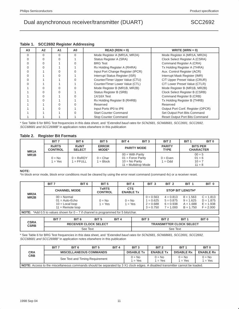
Table 1. SCC2692 Register AddressingA3 A2 A1 A0 READ (RDN = 0) WRITE (WRN = 0)
0 0 0 0 Mode Register A (MR1A, MR2A) Mode Register A (MR1A, MR2A)0 0 0 1 Status Register A (SRA) Clock Select Register A (CSRA)0 0 1 0 BRG Test Command Register A (CRA)0 0 1 1 Rx Holding Register A (RHRA) Tx Holding Register A (THRA)0 1 0 0 Input Port Change Register (IPCR) Aux. Control Register (ACR)0 1 0 1 Interrupt Status Register (ISR) Interrupt Mask Register (IMR)0 1 1 0 Counter/Timer Upper Value (CTU) C/T Upper Preset Value (CRUR)0 1 1 1 Counter/Timer Lower Value (CTL) C/T Lower Preset Value (CTLR)1 0 0 0 Mode Register B (MR1B, MR2B) Mode Register B (MR1B, MR2B)1 0 0 1 Status Register B (SRB) Clock Select Register B (CSRB)1 0 1 0 1X/16X Test Command Register B (CRB)1 0 1 1 Rx Holding Register B (RHRB) Tx Holding Register B (THRB)1 1 0 0 Reserved Reserved1 1 0 1 Input Ports IP0 to IP6 Output Port Conf. Register (OPCR)1 1 1 0 Start Counter Command Set Output Port Bits Command1 1 1 1 Stop Counter Command Reset Output Port Bits Command
* See Table 6 for BRG Test frequencies in this data sheet, and “Extended baud rates for SCN2681, SCN68681, SCC2691, SCC2692,SCC68681 and SCC2698B” in application notes elsewhere in this publication
Table 2. Register Bit FormatsBIT 7 BIT 6 BIT 5 BIT 4 BIT 3 BIT 2 BIT 1 BIT 0
MR1A
RxRTSCONTROL
RxINTSELECT
ERRORMODE* PARITY MODE PARITY
TYPEBITS PER
CHARACTERMR1AMR1B
0 = No1 = Yes
0 = RxRDY1 = FFULL
0 = Char1 = Block
00 = With Parity01 = Force Parity10 = No Parity11 = Multidrop Mode
0 = Even1 = Odd
00 = 501 = 610 = 711 = 8
NOTE:*In block error mode, block error conditions must be cleared by using the error reset command (command 4x) or a receiver reset.
BIT 7 BIT 6 BIT 5 BIT 4 BIT 3 BIT 2 BIT 1 BIT 0
MR2ACHANNEL MODE TxRTS
CONTROLCTS
ENABLE Tx STOP BIT LENGTH*MR2AMR2B 00 = Normal
01 = Auto-Echo10 = Local loop11 = Remote loop
0 = No1 = Yes
0 = No1 = Yes
0 = 0.563 4 = 0.813 8 = 1.563 C = 1.8131 = 0.625 5 = 0.875 9 = 1.625 D = 1.8752 = 0.688 6 = 0.938 A = 1.688 E = 1.9383 = 0.750 7 = 1.000 B = 1.750 F = 2.000
NOTE: *Add 0.5 to values shown for 0 – 7 if channel is programmed for 5 bits/char.
CSRABIT 7 BIT 6 BIT 5 BIT 4 BIT 3 BIT 2 BIT 1 BIT 0
CSRACSRB RECEIVER CLOCK SELECT TRANSMITTER CLOCK SELECTCSRB
See Text See Text
* See Table 6 for BRG Test frequencies in this data sheet, and “Extended baud rates for SCN2681, SCN68681, SCC2691, SCC2692,SCC68681 and SCC2698B” in application notes elsewhere in this publication
BIT 7 BIT 6 BIT 5 BIT 4 BIT 3 BIT 2 BIT 1 BIT 0
CRACRB
MISCELLANEOUS COMMANDS DISABLE Tx ENABLE Tx DISABLE Rx ENABLE RxCRB
See Text and Timing Requirement 0 = No1 = Yes
0 = No1 = Yes
0 = No1 = Yes
0 = No1 = Yes
NOTE: Access to the miscellaneous commands should be separated by 3 X1 clock edges. A disabled transmitter cannot be loaded.

Philips Semiconductors Product specification
SCC2692Dual asynchronous receiver/transmitter (DUART)
1998 Sep 04 12
Table 2. Register Bit Formats (Continued)
BIT 7 BIT 6 BIT 5 BIT 4 BIT 3 BIT 2 BIT 1 BIT 0
SRASRB
RECEIVEDBREAK*
FRAMINGERROR*
PARITYERROR*
OVERRUNERROR TxEMT TxRDY FFULL RxRDY
SRB0 = No1 = Yes
0 = No1 = Yes
0 = No1 = Yes
0 = No1 = Yes
0 = No1 = Yes
0 = No1 = Yes
0 = No1 = Yes
0 = No1 = Yes
NOTE: *These status bits are appended to the corresponding data character in the receive FIFO. A read of the status provides these bits(7:5) from the top of the FIFO together with bits (4:0). These bits are cleared by a “reset error status” command. In character mode they arediscarded when the corresponding data character is read from the FIFO. In block error mode, block error conditions must be cleared by usingthe error reset command (command 4x) or a receiver reset.
BIT 7 BIT 6 BIT 5 BIT 4 BIT 3 BIT 2 BIT 1 BIT 0
OP7 OP6 OP5 OP4 OP3 OP2
OPCR 0 = OPR[7]1 = TxRDYB
0 = OPR[6]1 = TxRDYA
0 = OPR[5]1 = RxRDY/ FFULLB
0 = OPR[4]1 = RxRDY/ FFULLA
00 = OPR[3]01 = C/T OUTPUT10 = TxCB(1X)11 = RxCB(1X)
00 = OPR[2]01 = TxCA(16X)10 = TxCA(1X)11 = RxCA(1X)
OPR BIT 7 BIT 6 BIT 5 BIT 4 BIT 3 BIT 2 BIT 1 BIT 0
OPR bit 0 1 0 1 0 1 0 1 0 1 0 1 0 1 0 1
OP pin 1 0 1 0 1 0 1 0 1 0 1 0 1 0 1 0
NOTE:The level at the OP pin is the inverse of the bit in the OPR register.
BIT 7 BIT 6 BIT 5 BIT 4 BIT 3 BIT 2 BIT 1 BIT 0
ACRBRG SETSELECT
COUNTER/TIMERMODE AND SOURCE
DELTAIP 3 INT
DELTAIP 2 INT
DELTAIP 1 INT
DELTAIP 0 INT
0 = set 11 = set 2 See Table 4 0 = Off
1 = On0 = Off1 = On
0 = Off1 = On
0 = Off1 = On
BIT 7 BIT 6 BIT 5 BIT 4 BIT 3 BIT 2 BIT 1 BIT 0
IPCRDELTA
IP 3DELTA
IP 2DELTA
IP 1DELTA
IP 0 IP 3 IP 2 IP 1 IP 0
0 = No1 = Yes
0 = No1 = Yes
0 = No1 = Yes
0 = No1 = Yes
0 = Low1 = High
0 = Low1 = High
0 = Low1 = High
0 = Low1 = High
BIT 7 BIT 6 BIT 5 BIT 4 BIT 3 BIT 2 BIT 1 BIT 0
ISR
INPUTPORT
CHANGE
DELTABREAK B
RxRDY/FFULLB TxRDYB COUNTER
READYDELTA
BREAK ARxRDY/FFULLA TxRDYA
0 = No1 = Yes
0 = No1 = Yes
0 = No1 = Yes
0 = No1 = Yes
0 = No1 = Yes
0 = No1 = Yes
0 = No1 = Yes
0 = No1 = Yes
BIT 7 BIT 6 BIT 5 BIT 4 BIT 3 BIT 2 BIT 1 BIT 0
IMR
IN. PORTCHANGE
INT
DELTABREAK B
INT
RxRDY/FFULLB
INT
TxRDYBINT
COUNTERREADY
INT
DELTABREAK A
INT
RxRDY/FFULLA
INT
TxRDYAINT
0 = Off1 = On
0 = Off1 = On
0 = Off1 = On
0 = Off1 = On
0 = Off1 = On
0 = Off1 = On
0 = Off1 = On
0 = Off1 = On
BIT 7 BIT 6 BIT 5 BIT 4 BIT 3 BIT 2 BIT 1 BIT 0
CTUR C/T[15] C/T[14] C/T[13] C/T[12] C/T[11] C/T[10] C/T[9] C/T[8]
BIT 7 BIT 6 BIT 5 BIT 4 BIT 3 BIT 2 BIT 1 BIT 0
CTLR C/T[7] C/T[6] C/T[5] C/T[4] C/T[3] C/T[2] C/T[1] C/T[0]

Philips Semiconductors Product specification
SCC2692Dual asynchronous receiver/transmitter (DUART)
1998 Sep 04 13
PROGRAMMINGThe operation of the DUART is programmed by writing control wordsinto the appropriate registers. Operational feedback is provided viastatus registers which can be read by the CPU. The addressing ofthe registers is described in Table 1.
The contents of certain control registers are initialized to zero onRESET. Care should be exercised if the contents of a register arechanged during operation, since certain changes may causeoperational problems.
For example, changing the number of bits per character while thetransmitter is active may cause the transmission of an incorrectcharacter. In general, the contents of the MR, the CSR, and theOPCR should only be changed while the receiver(s) andtransmitter(s) are not enabled, and certain changes to the ACRshould only be made while the C/T is stopped.
Mode registers 1 and 2 of each channel are accessed viaindependent auxiliary pointers. The pointer is set to MR1X byRESET or by issuing a ‘reset pointer’ command via thecorresponding command register. Any read or write of the moderegister while the pointer is at MR1X, switches the pointer to MR2X.The pointer then remains at MR2X, so that subsequent accessesare always to MR2X unless the pointer is reset to MR1X asdescribed above.
Mode, command, clock select, and status registers are duplicatedfor each channel to provide total independent operation and control.Refer to Table 2 for register bit descriptions. The reserved registersat addresses H‘02’ and H‘OA’ should never be read during normaloperation since they are reserved for internal diagnostics.
MR1A – Channel A Mode Register 1MR1A is accessed when the Channel A MR pointer points to MR1.The pointer is set to MR1 by RESET or by a ‘set pointer’ commandapplied via CRA. After reading or writing MR1A, the pointer will pointto MR2A.
MR1A[7] – Channel A Receiver Request-to-Send ControlThis bit controls the deactivation of the RTSAN output (OP0) by thereceiver. This output is normally asserted by setting OPR[0] andnegated by resetting OPR[0]. MR1A[7] = 1 causes RTSAN to benegated upon receipt of a valid start bit if the Channel A FIFO is full.However, OPR[0] is not reset and RTSAN will be asserted againwhen an empty FIFO position is available. This feature can be usedfor flow control to prevent overrun in the receiver by using theRTSAN output signal to control the CTSN input of the transmittingdevice.
MR1A[6] – Channel A Receiver Interrupt SelectThis bit selects either the Channel A receiver ready status (RxRDY)or the Channel A FIFO full status (FFULL) to be used for CPUinterrupts. It also causes the selected bit to be output on OP4 if it isprogrammed as an interrupt output via the OPCR.
MR1A[5] – Channel A Error Mode SelectThis bit selects the operating mode of the three FIFOed status bits(FE, PE, received break) for Channel A. In the ‘character’ mode,status is provided on a character-by-character basis; the statusapplies only to the character at the top of the FIFO. In the ‘block’mode, the status provided in the SR for these bits is theaccumulation (logical-OR) of the status for all characters coming tothe top of the FIFO since the last ‘reset error’ command for ChannelA was issued.
MR1A[4:3| – Channel A Parity Mode SelectIf ‘with parity’ or ‘force parity’ is selected a parity bit is added to thetransmitted character and the receiver performs a parity check onincoming data MR1A[4:3] = 11 selects Channel A to operate in thespecial multidrop mode described in the Operation section.
MR1A[2] – Channel A Parity Type SelectThis bit selects the parity type (odd or even) if the ‘with parity’ modeis programmed by MR1A[4:3], and the polarity of the forced parity bitif the ‘force parity’ mode is programmed. It has no effect if the ‘noparity’ mode is programmed. In the special multidrop mode it selectsthe polarity of the A/D bit.
MR1A[1:0] – Channel A Bits Per Character SelectThis field selects the number of data bits per character to betransmitted and received. The character length does not include thestart, parity, and stop bits.
MR2A – Channel A Mode Register 2MR2A is accessed when the Channel A MR pointer points to MR2,which occurs after any access to MR1A. Accesses to MR2A do notchange the pointer.
MR2A[7:6] – Channel A Mode SelectEach channel of the DUART can operate in one of four modes.MR2A[7:6] = 00 is the normal mode, with the transmitter andreceiver operating independently. MR2A[7:6] = 01 places thechannel in the automatic echo mode, which automaticallyre-transmits the received data. The following conditions are truewhile in automatic echo mode:1. Received data is re-clocked and retransmitted on the TxDA out-
put.
2. The receive clock is used for the transmitter.
3. The receiver must be enabled, but the transmitter need not beenabled.
4. The Channel A TxRDY and TxEMT status bits are inactive.
5. The received parity is checked, but is not regenerated for trans-mission, i.e., transmitted parity bit is as received.
6. Character framing is checked, but the stop bits are retransmittedas received.
7. A received break is echoed as received until the next valid startbit is detected.
8. CPU to receiver communication continues normally, but the CPUto transmitter link is disabled.
Two diagnostic modes can also be configured. MR2A[7:6] = 10selects local loopback mode. In this mode:1. The transmitter output is internally connected to the receiver
input.
2. The transmit clock is used for the receiver.
3. The TxDA output is held High.
4. The RxDA input is ignored.
5. The transmitter must be enabled, but the receiver need not beenabled.
6. CPU to transmitter and receiver communications continue nor-mally.
The second diagnostic mode is the remote loopback mode, selectedby MR2A[7:6] = 11. In this mode:

Philips Semiconductors Product specification
SCC2692Dual asynchronous receiver/transmitter (DUART)
1998 Sep 04 14
1. Received data is re-clocked and retransmitted on the TxDA out-put.
2. The receive clock is used for the transmitter.
3. Received data is not sent to the local CPU, and the error statusconditions are inactive.
4. The received parity is not checked and is not regenerated fortransmission, i.e., transmitted parity is as received.
5. The receiver must be enabled.
6. Character framing is not checked, and the stop bits are retrans-mitted as received.
7. A received break is echoed as received until the next valid startbit is detected.
The user must exercise care when switching into and out of thevarious modes. The selected mode will be activated immediatelyupon mode selection, even if this occurs in the middle of a receivedor transmitted character. Likewise, if a mode is deselected thedevice will switch out of the mode immediately. An exception to thisis switching out of autoecho or remote loopback modes: if thede-selection occurs just after the receiver has sampled the stop bit(indicated in autoecho by assertion of RxRDY), and the transmitteris enabled, the transmitter will remain in autoecho mode until theentire stop has been re-transmitted.
MR2A[5] – Channel A Transmitter Request-to-Send ControlCAUTION: When the transmitter controls the OP pin (usually usedfor the RTSN signal) the meaning of the pin is not RTSN at all!Rather, it signals that the transmitter has finished the transmission(i.e., end of block).
This bit allows deactivation of the RTSN output by the transmitter.This output is manually asserted and negated by the appropriatecommands issued via the command register. MR2[5] set to 1caused the RTSN to be reset automatically one bit time after thecharacter(s) in the transmit shift register and in the THR (if any) arecompletely transmitted (including the programmed number of stopbits) if a previously issued transmitter disable is pending. Thisfeature can be used to automatically terminate the transmission asfollows:
1. Program the auto-reset mode: MR2[5]=12. Enable transmitter, if not already enabled3. Assert RTSN via command4. Send message5. After the last character of the message is loaded to the THR,
disable the transmitter. (If the transmitter is underrun, a specialcase exists. See note below.)
6. The last character will be transmitted and the RTSN will be resetone bit time after the last stop bit is sent.
NOTE: The transmitter is in an underrun condition when both theTxRDY and the TxEMT bits are set. This condition also existsimmediately after the transmitter is enabled from the disabled orreset state. When using the above procedure with the transmitter inthe underrun condition, the issuing of the transmitter disable must bedelayed from the loading of a single, or last, character until theTxRDY becomes active again after the character is loaded.
MR2A[4] – Channel A Clear-to-Send ControlIf this bit is 0, CTSAN has no effect on the transmitter. If this bit is a1, the transmitter checks the state of CTSAN (IPO) each time it isready to send a character. If IPO is asserted (Low), the character istransmitted. If it is negated (High), the TxDA output remains in themarking state and the transmission is delayed until CTSAN goeslow. Changes in CTSAN while a character is being transmitted donot affect the transmission of that character..
MR2A[3:0] – Channel A Stop Bit Length SelectThis field programs the length of the stop bit appended to thetransmitted character. Stop bit lengths of 9/16 to 1 and 1-9/16 to 2bits, in increments of 1/16 bit, can be programmed for characterlengths of 6, 7, and 8 bits. For a character lengths of 5 bits, 1-1/16 to2 stop bits can be programmed in increments of 1/16 bit. In allcases, the receiver only checks for a ‘mark’ condition at the centerof the first stop bit position (one bit time after the last data bit, orafter the parity bit is enabled).
If an external 1X clock is used for the transmitter, MR2A[3] = 0selects one stop bit and MR2A[3] = 1 selects two stop bits to betransmitted.
Philips Semiconductors Product specification
SCC2692Dual asynchronous receiver/transmitter (DUART)
1998 Sep 04 15
MR1B – Channel B Mode Register 1MR1B is accessed when the Channel B MR pointer points to MR1.The pointer is set to MR1 by RESET or by a ‘set pointer’ commandapplied via CRB. After reading or writing MR1B, the pointer will pointto MR2B.
The bit definitions for this register are identical to MR1A, except thatall control actions apply to the Channel B receiver and transmitterand the corresponding inputs and outputs.
MR2B – Channel B Mode Register 2MR2B is accessed when the Channel B MR pointer points to MR2,which occurs after any access to MR1B. Accesses to MR2B do notchange the pointer.
The bit definitions for mode register are identical to the bitdefinitions for MR2A, except that all control actions apply to theChannel B receiver and transmitter and the corresponding inputsand outputs.
CSRA – Channel A Clock Select RegisterCSRA[7:4] – Channel A Receiver Clock SelectThis field selects the baud rate clock for the Channel A transmitter.The field definition is shown in Table 3.
CSRA[3:0] – Channel A Transmitter Clock SelectThis field selects the baud rate clock for the Channel A transmitter.The field definition is as shown in Table 3, except as follows:
CSRA[3:0] ACR[7] = 0 ACR[7] = 1
11101111
IP3-16XIP3-1X
IP3-16XIP3-1X
The transmitter clock is always a 16X clock except for CSRA[3:0] =1111.
Table 3. Baud RateCSRA[7:4] ACR[7] = 0 ACR[7] = 1
0000000100100011010001010110011110001001
50 110 134.5 200 300 6001,2001,0502,4004,800
75 110 134.5 150 300 6001,2002,0002,4004,800
101010111100110111101111
7,2009,60038.4KTimerIP4-16XIP4-1X
1,8009,60019.2KTimerIP4-16XIP4-1X
NOTE: The receiver clock is always a 16X clock except for CSRA[7:4]= 1111. Also, see Table 6 for baud rates available in BRG Test.
CSRB – Channel B Clock Select Register
CSRB[7:4] – Channel B Receiver Clock SelectThis field selects the baud rate clock for the Channel B receiver.The field definition is as shown in Table 3, except as follows:
CSRB[7:4] ACR[7] = 0 ACR[7] = 1
11101111
IP6-16XIP6-1X
IP6-16XIP6-1X
The receiver clock is always a 16X clock except for CSRB[7:4] = 1111.
CSRB[3:0] – Channel B Transmitter Clock SelectThis field selects the baud rate clock for the Channel B transmitter.The field definition is as shown in Table 3, except as follows:
CSRB[3:0] ACR[7] = 0 ACR[7] = 1
11101111
IP5-16XIP5-1X
IP5-16XIP5-1X
The transmitter clock is always a 16X clock except for CSRB[3:0] =1111.
CRA – Channel A Command RegisterCRA is a register used to supply commands to Channel A. Multiplecommands can be specified in a single write to CRA as long as thecommands are non-conflicting, e.g., the ‘enable transmitter’ and‘reset transmitter’ commands cannot be specified in a singlecommand word.
CRA[7:4] – Miscellaneous CommandsSequential writes to CR(7:4) should be separated by three edges ofthe X1 clock.
The encoded value of this field may be used to specify a singlecommand as follows:
0000 No command.0001 Reset MR pointer. Causes the Channel A MR pointer to point
to MR1.0010 Reset receiver. Resets the Channel A receiver as if a hard-
ware reset had been applied. The receiver is disabled and theFIFO is flushed.
0011 Reset transmitter. Resets the Channel A transmitter as if ahardware reset had been applied.
0100 Reset error status. Clears the Channel A Received Break,Parity Error, and Overrun Error bits in the status register(SRA[7:4]). Used in character mode to clear OE status (al-though RB, PE and FE bits will also be cleared) and in blockmode to clear all error status after a block of data has beenreceived.
0101 Reset Channel A break change interrupt. Causes the Chan-nel A break detect change bit in the interrupt status register(ISR[2]) to be cleared to zero.
0110 Start break. Forces the TxDA output Low (spacing). If thetransmitter is empty the start of the break condition will bedelayed up to two bit times. If the transmitter is active thebreak begins when transmission of the character is com-pleted. If a character is in the THR, the start of the break willbe delayed until that character, or any other loaded subse-quently are transmitted. The transmitter must be enabled forthis command to be accepted.
0111 Stop break. The TxDA line will go High (marking) within twobit times. TxDA will remain High for one bit time before thenext character, if any, is transmitted.
1000 Assert RTSN. Causes the RTSN output to be asserted (Low).1001 Negate RTSN. Causes the RTSN output to be negated
(High).1010 Set Timeout Mode On. The receiver in this channel will restart
the C/T as each receive character is transferred from the shiftregister to the RHR. The C/T is placed in the counter mode,the START/STOP counter commands are disabled, thecounter is stopped, and the Counter Ready Bit, ISR[3], isreset. The counter will not start until the first character is re-ceived after the command is issued.
1011 Not used.1100 Disable Timeout Mode. This command returns control of the
C/T to the regular START/STOP counter commands. It doesnot stop the counter, or clear any pending interrupts. Afterdisabling the timeout mode, a ‘Stop Counter’ commandshould be issued to reset the ISR(3) bit.
1101 Not used.
Philips Semiconductors Product specification
SCC2692Dual asynchronous receiver/transmitter (DUART)
1998 Sep 04 16
1110 Power Down Mode On. In this mode, the DUART oscillator isstopped and all functions requiring this clock are suspended.The execution of commands other than disable power downmode (1111) requires a X1/CLK. While in the power downmode, do not issue any commands to the CR except thedisable power down mode command. The contents of allregisters will be saved while in this mode. It is recommendedthat the transmitter and receiver be disabled prior to placingthe DUART into power down mode. This command is in CRAonly.
1111 Disable Power Down Mode. This command restarts the oscil-lator. After invoking this command, wait for the oscillator tostart up before writing further commands to the CR. Thiscommand is in CRA only.
CRA[3] – Disable Channel A TransmitterThis command terminates transmitter operation and resets theTxDRY and TxEMT status bits. However, if a character is beingtransmitted or if a character is in the THR when the transmitter isdisabled, the transmission of the character(s) is completed beforeassuming the inactive state.
CRA[2] – Enable Channel A TransmitterEnables operation of the Channel A transmitter. The TxRDY statusbit will be asserted.
CRA[1] – Disable Channel A ReceiverThis command terminates operation of the receiver immediately – acharacter being received will be lost. The command has no effect onthe receiver status bits or any other control registers. If the specialmultidrop mode is programmed, the receiver operates even if it isdisabled. See Operation section.
CRA[0] – Enable Channel A ReceiverEnables operation of the Channel A receiver. If not in the specialwake-up mode, this also forces the receiver into the search for startbit state.
CRB – Channel B Command RegisterCRB is a register used to supply commands to Channel B. Multiplecommands can be specified in a single write to CRB as long as thecommands are non-conflicting, e.g., the ‘enable transmitter’ and‘reset transmitter’ commands cannot be specified in a singlecommand word.
The bit definitions for this register are identical to the bit definitionsfor CRA, with the exception of commands “Ex” and “Fx” which areused for power downmode. These two commands are not used inCRB. All other control actions that apply to CRA also apply to CRB.
SRA – Channel A Status Register
SRA[7] – Channel A Received BreakThis bit indicates that an all zero character of the programmedlength has been received without a stop bit. Only a single FIFOposition is occupied when a break is received: further entries to theFIFO are inhibited until the RxDA line returns to the marking statefor at least one-half a bit time two successive edges of the internalor external 1X clock. This will usually require a high time of oneX1 clock period or 3 X1 edges since the clock of the controlleris not synchronous to the X1 clock.
When this bit is set, the Channel A ‘change in break’ bit in the ISR(ISR[2]) is set. ISR[2] is also set when the end of the breakcondition, as defined above, is detected.
The break detect circuitry can detect breaks that originate in themiddle of a received character. However, if a break begins in themiddle of a character, it must persist until at least the end of the nextcharacter time in order for it to be detected.
SRA[6] – Channel A Framing ErrorThis bit, when set, indicates that a stop bit was not detected whenthe corresponding data character in the FIFO was received. Thestop bit check is made in the middle of the first stop bit position.
SRA[5] – Channel A Parity ErrorThis bit is set when the ‘with parity’ or ‘force parity’ mode isprogrammed and the corresponding character in the FIFO wasreceived with incorrect parity.
In the special multidrop mode the parity error bit stores the receiveA/D bit.
SRA[4] – Channel A Overrun ErrorThis bit, when set, indicates that one or more characters in thereceived data stream have been lost. It is set upon receipt of a newcharacter when the FIFO is full and a character is already in thereceive shift register waiting for an empty FIFO position. When thisoccurs, the character in the receive shift register (and its breakdetect, parity error and framing error status, if any) is lost.
This bit is cleared by a ‘reset error status’ command.
SRA[3] – Channel A Transmitter Empty (TxEMTA)This bit will be set when the transmitter underruns, i.e., both theTxEMT and TxRDY bits are set. This bit and TxRDY are set whenthe transmitter is first enabled and at any time it is re-enabled aftereither (a) reset, or (b) the transmitter has assumed the disabledstate. It is always set after transmission of the last stop bit of acharacter if no character is in the THR awaiting transmission.
It is reset when the THR is loaded by the CPU, a pendingtransmitter disable is executed, the transmitter is reset, or thetransmitter is disabled while in the underrun condition.
SRA[2] – Channel A Transmitter Ready (TxRDYA)This bit, when set, indicates that the THR is empty and ready to beloaded with a character. This bit is cleared when the THR is loadedby the CPU and is set when the character is transferred to thetransmit shift register. TxRDY is reset when the transmitter isdisabled and is set when the transmitter is first enabled, e.g.,characters loaded into the THR while the transmitter is disabled willnot be transmitted.
SRA[1] – Channel A FIFO Full (FFULLA)This bit is set when a character is transferred from the receive shiftregister to the receive FIFO and the transfer causes the FIFO tobecome full, i.e., all three FIFO positions are occupied. It is resetwhen the CPU reads the RHR. If a character is waiting in thereceive shift register because the FIFO is full, FFULL will not bereset when the CPU reads the RHR.
SRA[0] – Channel A Receiver Ready (RxRDYA)This bit indicates that a character has been received and is waitingin the FIFO to be read by the CPU. It is set when the character istransferred from the receive shift to the FIFO and reset when theCPU reads the RHR, if after this read there are not more charactersstill in the FIFO.
SRB – Channel B Status RegisterThe bit definitions for this register are identical to the bit definitionsfor SRA, except that all status applies to the Channel B receiver andtransmitter and the corresponding inputs and outputs.
Philips Semiconductors Product specification
SCC2692Dual asynchronous receiver/transmitter (DUART)
1998 Sep 04 17
OPCR – Output Port Configuration Register
OPCR[7] – OP7 Output SelectThis bit programs the OP7 output to provide one of the following:0 The complement of OPR[7].1 The Channel B transmitter interrupt output which is the
complement of TxRDYB. When in this mode OP7 acts as anopen- drain output. Note that this output is not masked by thecontents of the IMR.
OPCR[6] – OP6 Output SelectThis bit programs the OP6 output to provide one of the following:0 The complement of OPR[6].1 The Channel A transmitter interrupt output which is the
complement of TxRDYA. When in this mode OP6 acts as anopen- drain output. Note that this output is not masked by thecontents of the IMR.
OPCR[5] – OP5 Output SelectThis bit programs the OP5 output to provide one of the following:0 The complement of OPR[5].1 The Channel B transmitter interrupt output which is the
complement of ISR[5]. When in this mode OP5 acts as anopen-drain output. Note that this output is not masked by thecontents of the IMR.
OPCR[4] – OP4 Output SelectThis field programs the OP4 output to provide one of the following:0 The complement of OPR[4].1 The Channel A receiver interrupt output which is the complement
of ISR[1]. When in this mode OP4 acts as an open-drain output.Note that this output is not masked by the contents of the IMR.
OPCR[3:2] – OP3 Output SelectThis bit programs the OP3 output to provide one of the following:00 The complement of OPR[3].01 The counter/timer output, in which case OP3 acts as an
open-drain output. In the timer mode, this output is a squarewave at the programmed frequency. In the counter mode, theoutput remains High until terminal count is reached, at whichtime it goes Low. The output returns to the High state when thecounter is stopped by a stop counter command. Note that thisoutput is not masked by the contents of the IMR.
10 The 1X clock for the Channel B transmitter, which is the clockthat shifts the transmitted data. If data is not being transmitted, afree running 1X clock is output.
11 The 1X clock for the Channel B receiver, which is the clock thatsamples the received data. If data is not being received, a freerunning 1X clock is output.
OPCR[1:0] – OP2 Output SelectThis field programs the OP2 output to provide one of the following:00 The complement of OPR[2].01 The 16X clock for the Channel A transmitter. This is the clock
selected by CSRA[3:0], and will be a 1X clock if CSRA[3:0] =1111.
10 The 1X clock for the Channel A transmitter, which is the clockthat shifts the transmitted data. If data is not being transmitted, afree running 1X clock is output.
11 The 1X clock for the Channel A receiver, which is the clock thatsamples the received data. If data is not being received, a freerunning 1X clock is output.
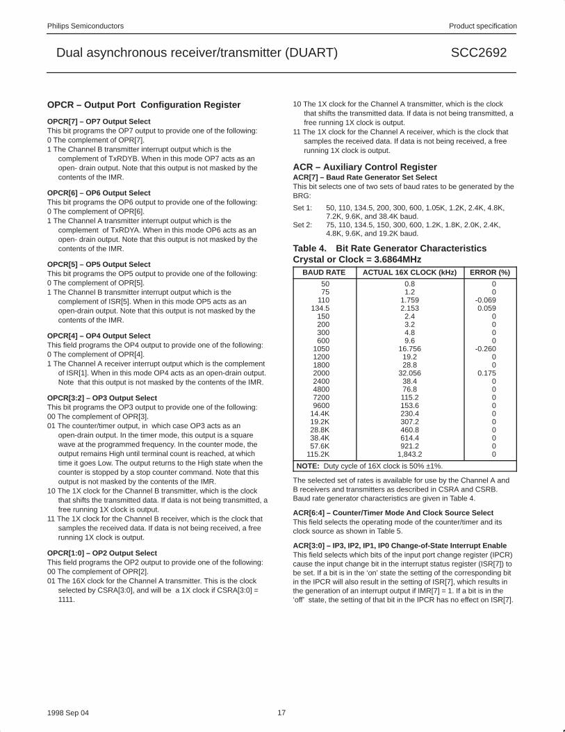
ACR – Auxiliary Control RegisterACR[7] – Baud Rate Generator Set SelectThis bit selects one of two sets of baud rates to be generated by theBRG:
Set 1: 50, 110, 134.5, 200, 300, 600, 1.05K, 1.2K, 2.4K, 4.8K,7.2K, 9.6K, and 38.4K baud.
Set 2: 75, 110, 134.5, 150, 300, 600, 1.2K, 1.8K, 2.0K, 2.4K,4.8K, 9.6K, and 19.2K baud.
Table 4. Bit Rate Generator CharacteristicsCrystal or Clock = 3.6864MHz
BAUD RATE ACTUAL 16X CLOCK (kHz) ERROR (%)
5075
110134.5
150200300600
10501200180020002400480072009600
14.4K19.2K28.8K38.4K57.6K
115.2K
0.81.2
1.7592.1532.43.24.89.6
16.75619.228.8
32.05638.476.8115.2153.6230.4307.2460.8614.4921.2
1,843.2
00
-0.0690.059
0000
-0.26000
0.1750000000000
NOTE: Duty cycle of 16X clock is 50% ±1%.
The selected set of rates is available for use by the Channel A andB receivers and transmitters as described in CSRA and CSRB.Baud rate generator characteristics are given in Table 4.
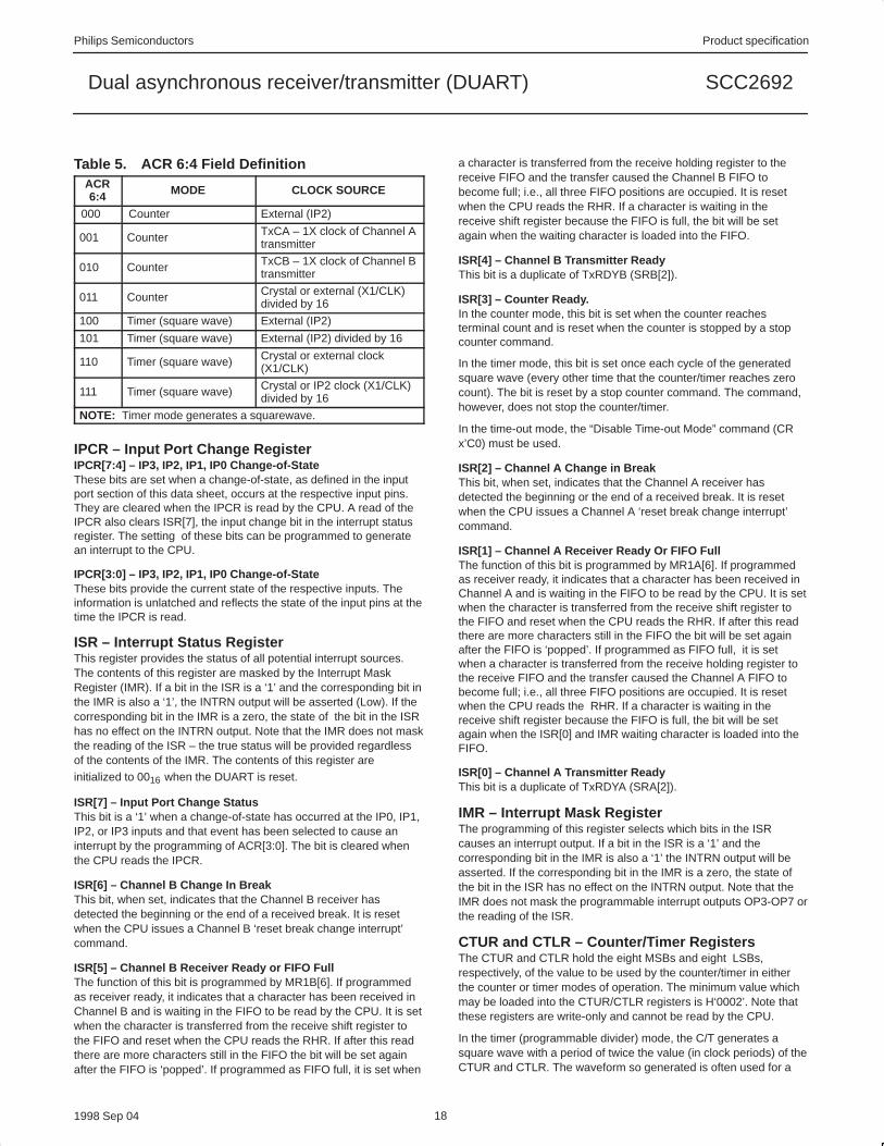
ACR[6:4] – Counter/Timer Mode And Clock Source SelectThis field selects the operating mode of the counter/timer and itsclock source as shown in Table 5.
ACR[3:0] – IP3, IP2, IP1, IP0 Change-of-State Interrupt EnableThis field selects which bits of the input port change register (IPCR)cause the input change bit in the interrupt status register (ISR[7]) tobe set. If a bit is in the ‘on’ state the setting of the corresponding bitin the IPCR will also result in the setting of ISR[7], which results inthe generation of an interrupt output if IMR[7] = 1. If a bit is in the‘off’ state, the setting of that bit in the IPCR has no effect on ISR[7].
Philips Semiconductors Product specification
SCC2692Dual asynchronous receiver/transmitter (DUART)
1998 Sep 04 18
Table 5. ACR 6:4 Field DefinitionACR6:4 MODE CLOCK SOURCE
000 Counter External (IP2)
001 Counter TxCA – 1X clock of Channel Atransmitter
010 Counter TxCB – 1X clock of Channel Btransmitter
011 Counter Crystal or external (X1/CLK)divided by 16
100 Timer (square wave) External (IP2)
101 Timer (square wave) External (IP2) divided by 16
110 Timer (square wave) Crystal or external clock(X1/CLK)
111 Timer (square wave) Crystal or IP2 clock (X1/CLK)divided by 16
NOTE: Timer mode generates a squarewave.
IPCR – Input Port Change RegisterIPCR[7:4] – IP3, IP2, IP1, IP0 Change-of-StateThese bits are set when a change-of-state, as defined in the inputport section of this data sheet, occurs at the respective input pins.They are cleared when the IPCR is read by the CPU. A read of theIPCR also clears ISR[7], the input change bit in the interrupt statusregister. The setting of these bits can be programmed to generatean interrupt to the CPU.
IPCR[3:0] – IP3, IP2, IP1, IP0 Change-of-StateThese bits provide the current state of the respective inputs. Theinformation is unlatched and reflects the state of the input pins at thetime the IPCR is read.
ISR – Interrupt Status RegisterThis register provides the status of all potential interrupt sources.The contents of this register are masked by the Interrupt MaskRegister (IMR). If a bit in the ISR is a ‘1’ and the corresponding bit inthe IMR is also a ‘1’, the INTRN output will be asserted (Low). If thecorresponding bit in the IMR is a zero, the state of the bit in the ISRhas no effect on the INTRN output. Note that the IMR does not maskthe reading of the ISR – the true status will be provided regardlessof the contents of the IMR. The contents of this register areinitialized to 0016 when the DUART is reset.
ISR[7] – Input Port Change StatusThis bit is a ‘1’ when a change-of-state has occurred at the IP0, IP1,IP2, or IP3 inputs and that event has been selected to cause aninterrupt by the programming of ACR[3:0]. The bit is cleared whenthe CPU reads the IPCR.
ISR[6] – Channel B Change In BreakThis bit, when set, indicates that the Channel B receiver hasdetected the beginning or the end of a received break. It is resetwhen the CPU issues a Channel B ‘reset break change interrupt’command.
ISR[5] – Channel B Receiver Ready or FIFO FullThe function of this bit is programmed by MR1B[6]. If programmedas receiver ready, it indicates that a character has been received inChannel B and is waiting in the FIFO to be read by the CPU. It is setwhen the character is transferred from the receive shift register tothe FIFO and reset when the CPU reads the RHR. If after this readthere are more characters still in the FIFO the bit will be set againafter the FIFO is ‘popped’. If programmed as FIFO full, it is set when
a character is transferred from the receive holding register to thereceive FIFO and the transfer caused the Channel B FIFO tobecome full; i.e., all three FIFO positions are occupied. It is resetwhen the CPU reads the RHR. If a character is waiting in thereceive shift register because the FIFO is full, the bit will be setagain when the waiting character is loaded into the FIFO.
ISR[4] – Channel B Transmitter ReadyThis bit is a duplicate of TxRDYB (SRB[2]).
ISR[3] – Counter Ready.In the counter mode, this bit is set when the counter reachesterminal count and is reset when the counter is stopped by a stopcounter command.
In the timer mode, this bit is set once each cycle of the generatedsquare wave (every other time that the counter/timer reaches zerocount). The bit is reset by a stop counter command. The command,however, does not stop the counter/timer.
In the time-out mode, the “Disable Time-out Mode” command (CRx’C0) must be used.
ISR[2] – Channel A Change in BreakThis bit, when set, indicates that the Channel A receiver hasdetected the beginning or the end of a received break. It is resetwhen the CPU issues a Channel A ‘reset break change interrupt’command.
ISR[1] – Channel A Receiver Ready Or FIFO FullThe function of this bit is programmed by MR1A[6]. If programmedas receiver ready, it indicates that a character has been received inChannel A and is waiting in the FIFO to be read by the CPU. It is setwhen the character is transferred from the receive shift register tothe FIFO and reset when the CPU reads the RHR. If after this readthere are more characters still in the FIFO the bit will be set againafter the FIFO is ‘popped’. If programmed as FIFO full, it is setwhen a character is transferred from the receive holding register tothe receive FIFO and the transfer caused the Channel A FIFO tobecome full; i.e., all three FIFO positions are occupied. It is resetwhen the CPU reads the RHR. If a character is waiting in thereceive shift register because the FIFO is full, the bit will be setagain when the ISR[0] and IMR waiting character is loaded into theFIFO.
ISR[0] – Channel A Transmitter ReadyThis bit is a duplicate of TxRDYA (SRA[2]).
IMR – Interrupt Mask RegisterThe programming of this register selects which bits in the ISRcauses an interrupt output. If a bit in the ISR is a ‘1’ and thecorresponding bit in the IMR is also a ‘1’ the INTRN output will beasserted. If the corresponding bit in the IMR is a zero, the state ofthe bit in the ISR has no effect on the INTRN output. Note that theIMR does not mask the programmable interrupt outputs OP3-OP7 orthe reading of the ISR.
CTUR and CTLR – Counter/Timer RegistersThe CTUR and CTLR hold the eight MSBs and eight LSBs,respectively, of the value to be used by the counter/timer in eitherthe counter or timer modes of operation. The minimum value whichmay be loaded into the CTUR/CTLR registers is H‘0002’. Note thatthese registers are write-only and cannot be read by the CPU.
In the timer (programmable divider) mode, the C/T generates asquare wave with a period of twice the value (in clock periods) of theCTUR and CTLR. The waveform so generated is often used for a
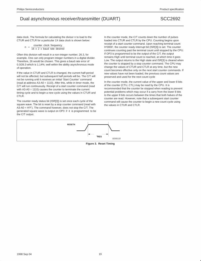
Philips Semiconductors Product specification
SCC2692Dual asynchronous receiver/transmitter (DUART)
1998 Sep 04 19
data clock. The formula for calculating the divisor n to load to theCTUR and CTLR for a particular 1X data clock is shown below:
n
counter clock frequency16 x 2 x baud rate desired
Often this division will result in a non-integer number; 26.3, forexample. One can only program integer numbers in a digital divider.Therefore, 26 would be chosen. This gives a baud rate error of0.3/26.3 which is 1.14%; well within the ability asynchronous modeof operation.
If the value in CTUR and CTLR is changed, the current half-periodwill not be affected, but subsequent half periods will be. The C/T willnot be running until it receives an initial ‘Start Counter’ command(read at address A3-A0 = 1110). After this, while in timer mode, theC/T will run continuously. Receipt of a start counter command (readwith A3-A0 = 1110) causes the counter to terminate the currenttiming cycle and to begin a new cycle using the values in CTUR andCTLR.
The counter ready status bit (ISR[3]) is set once each cycle of thesquare wave. The bit is reset by a stop counter command (read withA3-A0 = H‘F’). The command however, does not stop the C/T. Thegenerated square wave is output on OP3 if it is programmed to bethe C/T output.
In the counter mode, the C/T counts down the number of pulsesloaded into CTUR and CTLR by the CPU. Counting begins uponreceipt of a start counter command. Upon reaching terminal countH‘0000’, the counter ready interrupt bit (ISR[3]) is set. The countercontinues counting past the terminal count until stopped by the CPU.If OP3 is programmed to be the output of the C/T, the outputremains High until terminal count is reached, at which time it goesLow. The output returns to the High state and ISR[3] is cleared whenthe counter is stopped by a stop counter command. The CPU maychange the values of CTUR and CTLR at any time, but the newcount becomes effective only on the next start counter commands. Ifnew values have not been loaded, the previous count values arepreserved and used for the next count cycle
In the counter mode, the current value of the upper and lower 8 bitsof the counter (CTU, CTL) may be read by the CPU. It isrecommended that the counter be stopped when reading to preventpotential problems which may occur if a carry from the lower 8 bitsto the upper 8 bits occurs between the times that both halves of thecounter are read. However, note that a subsequent start countercommand will cause the counter to begin a new count cycle usingthe values in CTUR and CTLR.
RESETN
tRESSD00133
Figure 3. Reset Timing
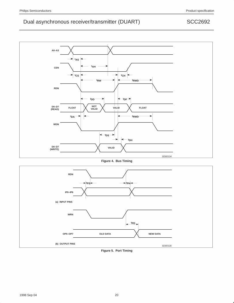
Philips Semiconductors Product specification
SCC2692Dual asynchronous receiver/transmitter (DUART)
1998 Sep 04 20
A0–A3
CEN
tAS
tCS tCH
RDN
tRW tRWD
D0–D7(READ)
tDD tDF
FLOAT FLOATVALIDNOT
VALID
WDN
tRWD
VALIDD0–D7(WRITE)
tDS
tDH
tAH
tDA
SD00134
Figure 4. Bus Timing
(b) OUTPUT PINS
RDN
IP0–IP6
WRN
OP0–OP7
tPS tPH
tPD
OLD DATA NEW DATA
(a) INPUT PINS
SD00135
Figure 5. Port Timing

Philips Semiconductors Product specification
SCC2692Dual asynchronous receiver/transmitter (DUART)
1998 Sep 04 21
NOTES:1. INTRN or OP3-OP7 when used as interrupt outputs.2. The test for open-drain outputs is intended to guarantee switching of the output transistor. Measurement of this response is referenced from the midpoint of the switching
signal, VM, to a point 0.5V above VOL. This point represents noise margin that assures true switching has occurred. Beyond this level, the effects of external circuitry andtest environment are pronounced and can greatly affect the resultant measurement.
VM
VOL +0.5V
VOL
WRN
INTERRUPT1
OUTPUT
tIR
VM
VOL +0.5V
VOL
RDN
INTERRUPT1
OUTPUT
tIR
SD00136
Figure 6. Interrupt Timing
X1/CLKCTCLK
RxCTxC
tCLKtCTCtRxtTx
tCLKtCTCtRxtTx
+5V
1K
X1
X2
C1 = C2 = 24pF FOR CL = 20PF
X1
X2
3.6864MHz
3pF
4pF
50 TO150 KΩ
TO INTERNAL CLOCK DRIVERS
SCC2698B
NOTE:C1 AND C2 SHOULD BE BASED ON MANUFACTURER’S SPECIFICATION. PARASITIC CAPACITANCE SHOULDBE INCLUDED WITH C1 AND C2. R1 IS ONLY REQUIRED IF U1 WILL NOT DRIVE TO X1 INPUT LEVELS
TYPICAL CRYSTAL SPECIFICATIONFREQUENCY: 2 – 4MHZLOAD CAPACITANCE (C L): 12 – 32pFTYPE OF OPERATION: PARALLEL RESONANT, FUNDAMENTAL MODE
NC
R1
U1
SD00137
RESISTOR REQUIREDWHEN U1 IS A TTL DEVICE
Figure 7. Clock Timing
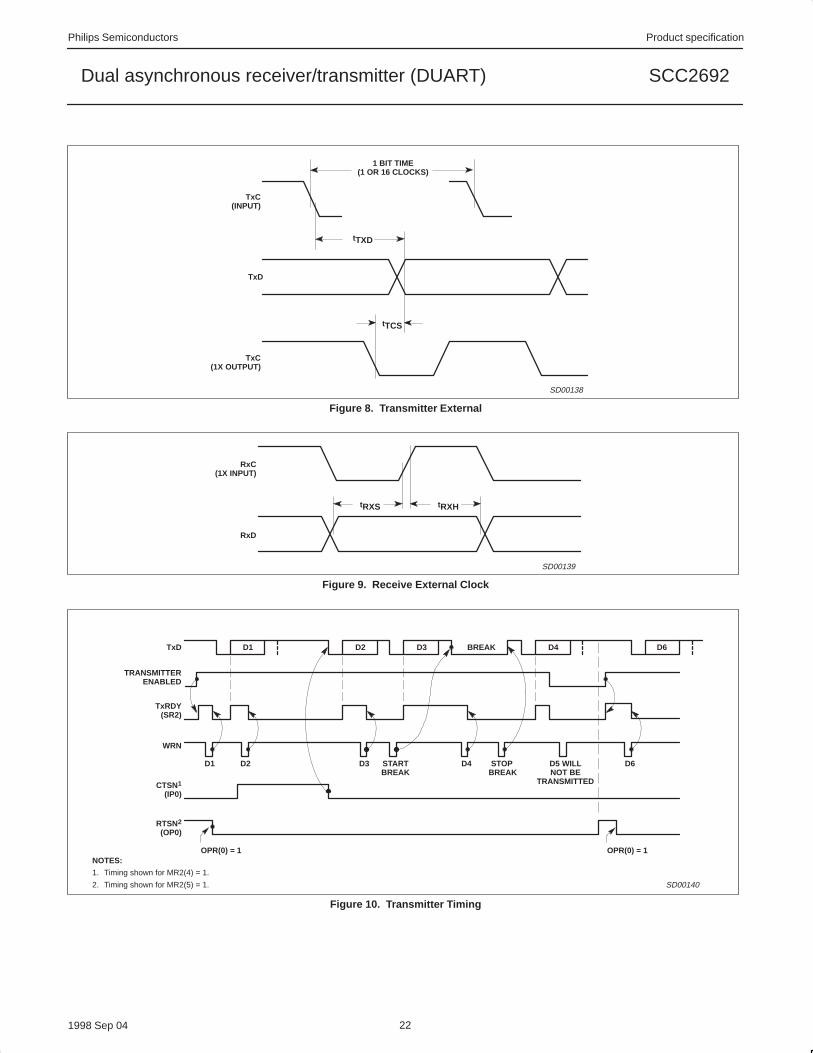
Philips Semiconductors Product specification
SCC2692Dual asynchronous receiver/transmitter (DUART)
1998 Sep 04 22
tTXD
tTCS
1 BIT TIME(1 OR 16 CLOCKS)
TxD
TxC(INPUT)
TxC(1X OUTPUT)
SD00138
Figure 8. Transmitter External
tRXS tRXH
RxC(1X INPUT)
RxD
SD00139
Figure 9. Receive External Clock
TRANSMITTERENABLED
TxD D1 D2 D3 D4 D6BREAK
TxRDY(SR2)
WRN
D1 D2 D3 D4 D6STARTBREAK
STOP BREAK
D5 WILLNOT BE
TRANSMITTEDCTSN1
(IP0)
RTSN2
(OP0)
OPR(0) = 1 OPR(0) = 1NOTES:
1. Timing shown for MR2(4) = 1.
2. Timing shown for MR2(5) = 1. SD00140
Figure 10. Transmitter Timing
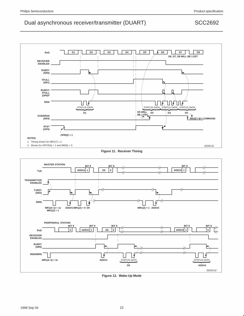
Philips Semiconductors Product specification
SCC2692Dual asynchronous receiver/transmitter (DUART)
1998 Sep 04 23
D1 D2 D3 D4 D5 D6 D7 D8RxD
D6, D7, D8 WILL BE LOST
RECEIVERENABLED
RxRDY(SR0)
FFULL(SR1)
RxRDY/FFULL(OP5)2
RDN
STATUS DATA
D1
STATUS DATA
D2
STATUS DATA
D3
STATUS DATA
D4D5 WILLBE LOSTOVERRUN
(SR4) RESET BY COMMAND
RTS1
(OP0)
OPR(0) = 1NOTES:
1. Timing shown for MR1(7) = 1.
2. Shown for OPCR(4) = 1 and MR(6) = 0. SD00141
Figure 11. Receiver Timing
TRANSMITTERENABLED
TxD ADD#1
TxRDY(SR2)
WRN
MR1(4–3) = 11MR1(2) = 1
1
BIT 9
D0 0
BIT 9
ADD#2 1
BIT 9MASTER STATION
ADD#1 MR1(2) = 0 D0 MR1(2) = 1 ADD#2
RxD ADD#1 1
BIT 9
D0 0
BIT 9
ADD#2 1
BIT 9PERIPHERAL STATION
0
BIT 9
0
BIT 9
RECEIVERENABLED
RxRDY(SR0)
RDN/WRN
MR1(4–3) = 11 ADD#1 STATUS DATA
D0
STATUS DATA
ADD#2
SD00142
Figure 12. Wake-Up Mode
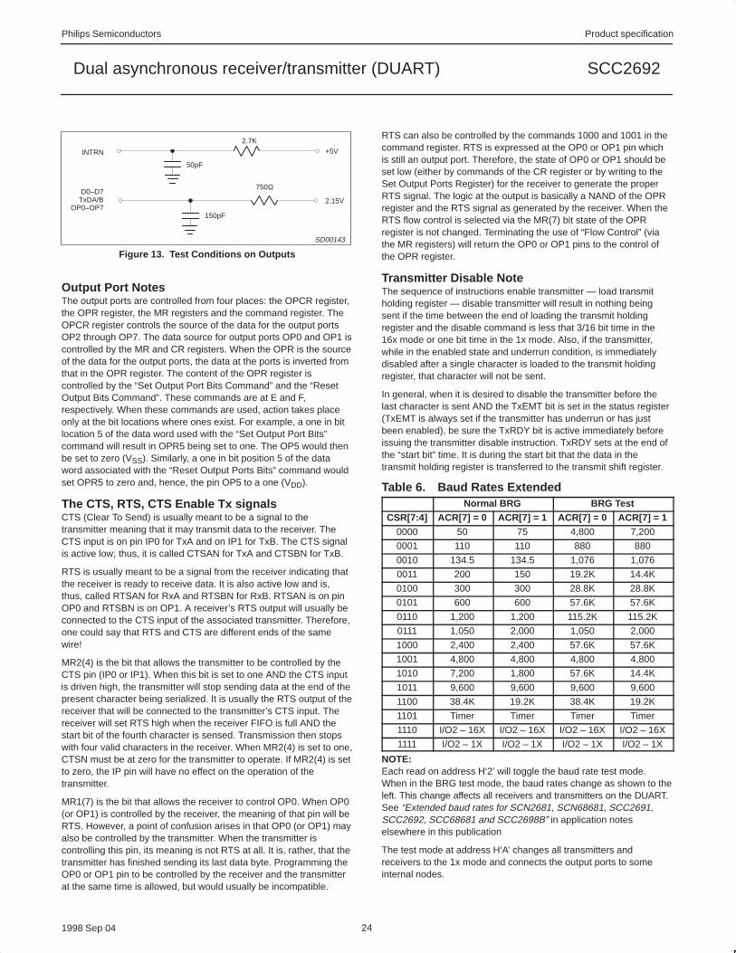
Philips Semiconductors Product specification
SCC2692Dual asynchronous receiver/transmitter (DUART)
1998 Sep 04 24
INTRN
D0–D7TxDA/B
OP0–OP7150pF
2.15V
750Ω
50pF
+5V
2.7K
SD00143
Figure 13. Test Conditions on Outputs
Output Port NotesThe output ports are controlled from four places: the OPCR register,the OPR register, the MR registers and the command register. TheOPCR register controls the source of the data for the output portsOP2 through OP7. The data source for output ports OP0 and OP1 iscontrolled by the MR and CR registers. When the OPR is the sourceof the data for the output ports, the data at the ports is inverted fromthat in the OPR register. The content of the OPR register iscontrolled by the “Set Output Port Bits Command” and the “ResetOutput Bits Command”. These commands are at E and F,respectively. When these commands are used, action takes placeonly at the bit locations where ones exist. For example, a one in bitlocation 5 of the data word used with the “Set Output Port Bits”command will result in OPR5 being set to one. The OP5 would thenbe set to zero (VSS). Similarly, a one in bit position 5 of the dataword associated with the “Reset Output Ports Bits” command wouldset OPR5 to zero and, hence, the pin OP5 to a one (VDD).
The CTS, RTS, CTS Enable Tx signalsCTS (Clear To Send) is usually meant to be a signal to thetransmitter meaning that it may transmit data to the receiver. TheCTS input is on pin IP0 for TxA and on IP1 for TxB. The CTS signalis active low; thus, it is called CTSAN for TxA and CTSBN for TxB.
RTS is usually meant to be a signal from the receiver indicating thatthe receiver is ready to receive data. It is also active low and is,thus, called RTSAN for RxA and RTSBN for RxB. RTSAN is on pinOP0 and RTSBN is on OP1. A receiver’s RTS output will usually beconnected to the CTS input of the associated transmitter. Therefore,one could say that RTS and CTS are different ends of the samewire!
MR2(4) is the bit that allows the transmitter to be controlled by theCTS pin (IP0 or IP1). When this bit is set to one AND the CTS inputis driven high, the transmitter will stop sending data at the end of thepresent character being serialized. It is usually the RTS output of thereceiver that will be connected to the transmitter’s CTS input. Thereceiver will set RTS high when the receiver FIFO is full AND thestart bit of the fourth character is sensed. Transmission then stopswith four valid characters in the receiver. When MR2(4) is set to one,CTSN must be at zero for the transmitter to operate. If MR2(4) is setto zero, the IP pin will have no effect on the operation of thetransmitter.
MR1(7) is the bit that allows the receiver to control OP0. When OP0(or OP1) is controlled by the receiver, the meaning of that pin will beRTS. However, a point of confusion arises in that OP0 (or OP1) mayalso be controlled by the transmitter. When the transmitter iscontrolling this pin, its meaning is not RTS at all. It is, rather, that thetransmitter has finished sending its last data byte. Programming theOP0 or OP1 pin to be controlled by the receiver and the transmitterat the same time is allowed, but would usually be incompatible.
RTS can also be controlled by the commands 1000 and 1001 in thecommand register. RTS is expressed at the OP0 or OP1 pin whichis still an output port. Therefore, the state of OP0 or OP1 should beset low (either by commands of the CR register or by writing to theSet Output Ports Register) for the receiver to generate the properRTS signal. The logic at the output is basically a NAND of the OPRregister and the RTS signal as generated by the receiver. When theRTS flow control is selected via the MR(7) bit state of the OPRregister is not changed. Terminating the use of “Flow Control” (viathe MR registers) will return the OP0 or OP1 pins to the control ofthe OPR register.
Transmitter Disable NoteThe sequence of instructions enable transmitter — load transmitholding register — disable transmitter will result in nothing beingsent if the time between the end of loading the transmit holdingregister and the disable command is less that 3/16 bit time in the16x mode or one bit time in the 1x mode. Also, if the transmitter,while in the enabled state and underrun condition, is immediatelydisabled after a single character is loaded to the transmit holdingregister, that character will not be sent.
In general, when it is desired to disable the transmitter before thelast character is sent AND the TxEMT bit is set in the status register(TxEMT is always set if the transmitter has underrun or has justbeen enabled), be sure the TxRDY bit is active immediately beforeissuing the transmitter disable instruction. TxRDY sets at the end ofthe “start bit” time. It is during the start bit that the data in thetransmit holding register is transferred to the transmit shift register.
Table 6. Baud Rates ExtendedNormal BRG BRG Test
CSR[7:4] ACR[7] = 0 ACR[7] = 1 ACR[7] = 0 ACR[7] = 10000 50 75 4,800 7,200
0001 110 110 880 880
0010 134.5 134.5 1,076 1,076
0011 200 150 19.2K 14.4K
0100 300 300 28.8K 28.8K
0101 600 600 57.6K 57.6K
0110 1,200 1,200 115.2K 115.2K
0111 1,050 2,000 1,050 2,000
1000 2,400 2,400 57.6K 57.6K
1001 4,800 4,800 4,800 4,800
1010 7,200 1,800 57.6K 14.4K
1011 9,600 9,600 9,600 9,600
1100 38.4K 19.2K 38.4K 19.2K
1101 Timer Timer Timer Timer
1110 I/O2 – 16X I/O2 – 16X I/O2 – 16X I/O2 – 16X
1111 I/O2 – 1X I/O2 – 1X I/O2 – 1X I/O2 – 1X
NOTE:Each read on address H‘2’ will toggle the baud rate test mode.When in the BRG test mode, the baud rates change as shown to theleft. This change affects all receivers and transmitters on the DUART.See “Extended baud rates for SCN2681, SCN68681, SCC2691,SCC2692, SCC68681 and SCC2698B” in application noteselsewhere in this publication
The test mode at address H‘A’ changes all transmitters andreceivers to the 1x mode and connects the output ports to someinternal nodes.
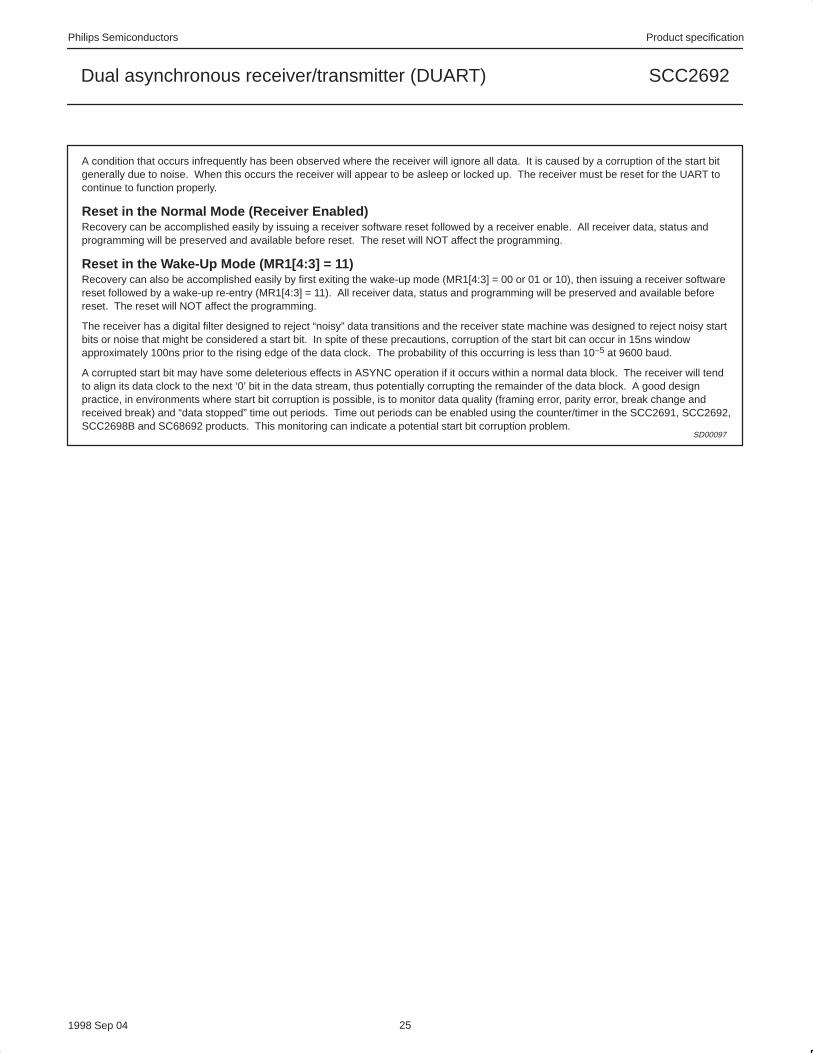
Philips Semiconductors Product specification
SCC2692Dual asynchronous receiver/transmitter (DUART)
1998 Sep 04 25
A condition that occurs infrequently has been observed where the receiver will ignore all data. It is caused by a corruption of the start bitgenerally due to noise. When this occurs the receiver will appear to be asleep or locked up. The receiver must be reset for the UART tocontinue to function properly.
Reset in the Normal Mode (Receiver Enabled)Recovery can be accomplished easily by issuing a receiver software reset followed by a receiver enable. All receiver data, status andprogramming will be preserved and available before reset. The reset will NOT affect the programming.
Reset in the Wake-Up Mode (MR1[4:3] = 11)Recovery can also be accomplished easily by first exiting the wake-up mode (MR1[4:3] = 00 or 01 or 10), then issuing a receiver softwarereset followed by a wake-up re-entry (MR1[4:3] = 11). All receiver data, status and programming will be preserved and available beforereset. The reset will NOT affect the programming.
The receiver has a digital filter designed to reject “noisy” data transitions and the receiver state machine was designed to reject noisy startbits or noise that might be considered a start bit. In spite of these precautions, corruption of the start bit can occur in 15ns windowapproximately 100ns prior to the rising edge of the data clock. The probability of this occurring is less than 10–5 at 9600 baud.
A corrupted start bit may have some deleterious effects in ASYNC operation if it occurs within a normal data block. The receiver will tendto align its data clock to the next ‘0’ bit in the data stream, thus potentially corrupting the remainder of the data block. A good designpractice, in environments where start bit corruption is possible, is to monitor data quality (framing error, parity error, break change andreceived break) and “data stopped” time out periods. Time out periods can be enabled using the counter/timer in the SCC2691, SCC2692,SCC2698B and SC68692 products. This monitoring can indicate a potential start bit corruption problem.
SD00097

Philips Semiconductors Product specification
SCC2692Dual asynchronous receiver/transmitter (DUART)
1998 Sep 04 26
DIP40: plastic dual in-line package; 40 leads (600 mil) SOT129-1

Philips Semiconductors Product specification
SCC2692Dual asynchronous receiver/transmitter (DUART)
1998 Sep 04 27
DIP28: plastic dual in-line package; 28 leads (600 mil) SOT117-1
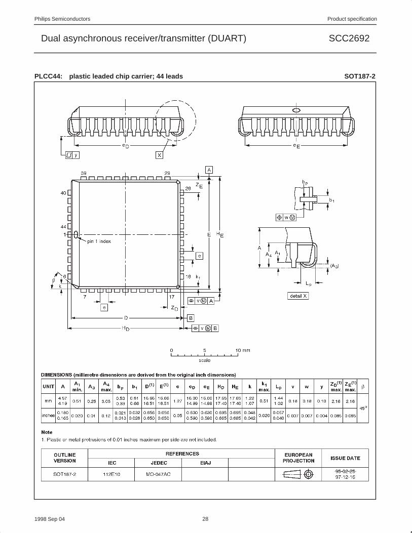
Philips Semiconductors Product specification
SCC2692Dual asynchronous receiver/transmitter (DUART)
1998 Sep 04 28
PLCC44: plastic leaded chip carrier; 44 leads SOT187-2
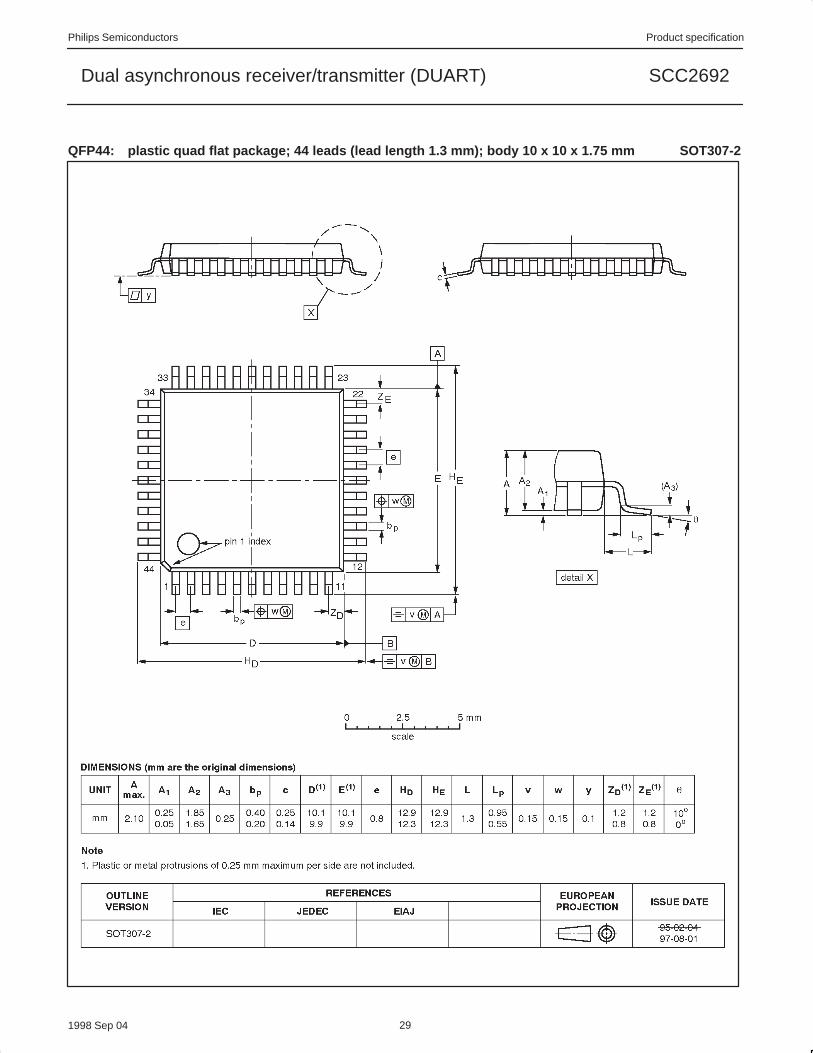
Philips Semiconductors Product specification
SCC2692Dual asynchronous receiver/transmitter (DUART)
1998 Sep 04 29
QFP44: plastic quad flat package; 44 leads (lead length 1.3 mm); body 10 x 10 x 1.75 mm SOT307-2
Philips Semiconductors Product specification
SCC2692Dual asynchronous receiver/transmitter (DUART)
1998 Sep 04 30
DefinitionsShort-form specification — The data in a short-form specification is extracted from a full data sheet with the same type number and title. Fordetailed information see the relevant data sheet or data handbook.
Limiting values definition — Limiting values given are in accordance with the Absolute Maximum Rating System (IEC 134). Stress above oneor more of the limiting values may cause permanent damage to the device. These are stress ratings only and operation of the device at these orat any other conditions above those given in the Characteristics sections of the specification is not implied. Exposure to limiting values for extendedperiods may affect device reliability.
Application information — Applications that are described herein for any of these products are for illustrative purposes only. PhilipsSemiconductors make no representation or warranty that such applications will be suitable for the specified use without further testing ormodification.
DisclaimersLife support — These products are not designed for use in life support appliances, devices or systems where malfunction of these products canreasonably be expected to result in personal injury. Philips Semiconductors customers using or selling these products for use in such applicationsdo so at their own risk and agree to fully indemnify Philips Semiconductors for any damages resulting from such application.
Right to make changes — Philips Semiconductors reserves the right to make changes, without notice, in the products, including circuits, standardcells, and/or software, described or contained herein in order to improve design and/or performance. Philips Semiconductors assumes noresponsibility or liability for the use of any of these products, conveys no license or title under any patent, copyright, or mask work right to theseproducts, and makes no representations or warranties that these products are free from patent, copyright, or mask work right infringement, unlessotherwise specified.
Philips Semiconductors811 East Arques AvenueP.O. Box 3409Sunnyvale, California 94088–3409Telephone 800-234-7381
Copyright Philips Electronics North America Corporation 1998All rights reserved. Printed in U.S.A.
Date of release: 09-98
Document order number: 9397 750 04359
Data sheetstatus
Objective specification
Preliminary specification
Product specification
Productstatus
Development
Qualification
Production
Definition [1]
This data sheet contains the design target or goal specifications for product development.Specification may change in any manner without notice.
This data sheet contains preliminary data, and supplementary data will be published at a later date.Philips Semiconductors reserves the right to make chages at any time without notice in order toimprove design and supply the best possible product.
This data sheet contains final specifications. Philips Semiconductors reserves the right to makechanges at any time without notice in order to improve design and supply the best possible product.
Data sheet status
[1] Please consult the most recently issued datasheet before initiating or completing a design.