1
Topology System
Uli Schäfer
B.Bauß, V.Büscher, W.Ji, U.Schäfer, A.Reiß, E.Simioni, S.Tapprogge, V.Wenzel

2
Topology 2013/14 (RTDP)
Uli Schäfer
Topo Processor
Muons
Legacy electrical links
Cluster Processor
CMX
CTPCore
Jet/Energy Processor
CMX
From PPr / nMCMs
6.4Gb/s fibre bundles
Fibre & 32 electrical LVDS links
160 /
12 /

3
Topology Processor
To provide a maximum of flexibility for applying topological trigger criteria
• All Level-1 topo trigger signals into a single module• Allow to correlate all trigger object types within full solid
angle• e/m clusters, tau• Jets• Missing Energy• Small volume of muon signals from 2014
• Ample logic resources to run many algorithms in parallel
• Option to run separate algorithms on more than one topology module in parallel
Uli Schäfer

4
Topo processor features• AdvancedTCA form factor• High input bandwidth (@ 6.4Gb/s baseline input rate, 2014)
• Electrons, tau, jets, MET : 553 Gb/s• Muons 267 Gb/s • Total aggregate bandwidth 820 Gb/s
• Low processing latency on real-time path• On-FPGA multi-gigabit links (MGTs)• High density 12-channel opto transceivers (miniPODs)• Fibre bundles from L1Calo mergers (CMXes)• Fibre bundle and low latency LVDS into CTPcore
• Well prepared for phase 1: • accept line rates above 6.4Gb/s from future processors
(FEXes, muons)• Employ zero suppression
Uli Schäfer

5
Topology Processor Schedule
Uli Schäfer
2010 2011 2012 2013 2014
Technology Demonstrator (BLT)
Functional Demonstrator (GOLD)
Prototype
Installation
GOLD delivery
Production Completed
Production module
Prototype production
Review June 12(report : see EDMS)

6
Functional Demonstrator : “GOLD”
• Fibre input from the backplane (MTP-CPI connectors)• 10Gb/s 12-channel industry standard o/e converters on mezzanine• High performance FPGAs (XC6VLX240T) with multiple 6.4Gb/s
transceivers• Real-time output via opto links on the front panel
Uli Schäfer

7
GOLD test results and plansCharacterization of Optical Links● “MGT/AVAGO” settingsBit Error Rate (BER) < 10-16 @6.4GBits/s / 12 channels(conditions on GOLD are tougher, mezzanine connectors and long traces)
Uli Schäfer

8
GOLD test results and plansCurrent Algorithm Implementation Efforts● Implementation of dphi Leading Jet Algorithm exists for simulation and hardware in the GOLD● First estimate of logic usage: about 10% of (small) XC6VLX240T
● Implement toy data source for dphi alg. Determine Latency Logic Usage PMA loop back test● Prepare existing FW for Virtex-7 as far as possible (L1Topo)● We continue to use GOLD while prototype is being built
Uli Schäfer
9
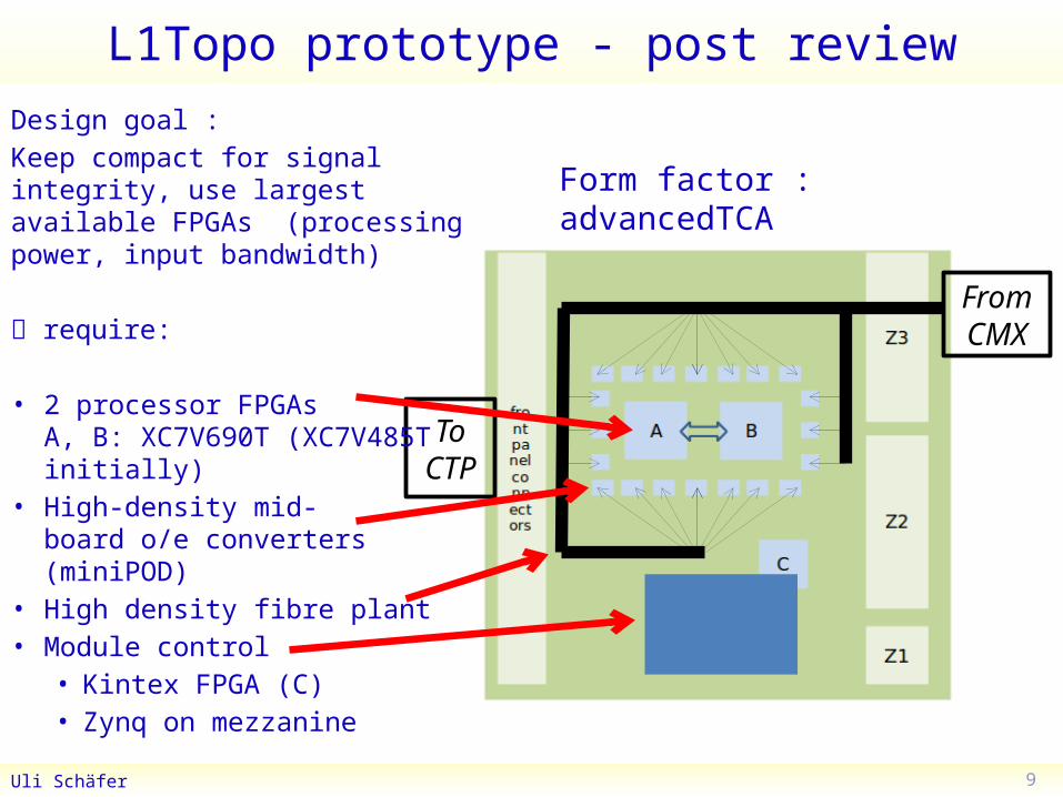
L1Topo prototype - post review
Uli Schäfer
From CMX
To CTP
Design goal : Keep compact for signal integrity, use largest available FPGAs (processing power, input bandwidth)
require:
• 2 processor FPGAs A, B: XC7V690T (XC7V485T initially)
• High-density mid-board o/e converters (miniPOD)
• High density fibre plant• Module control
• Kintex FPGA (C)• Zynq on mezzanine
Form factor : advancedTCA
10
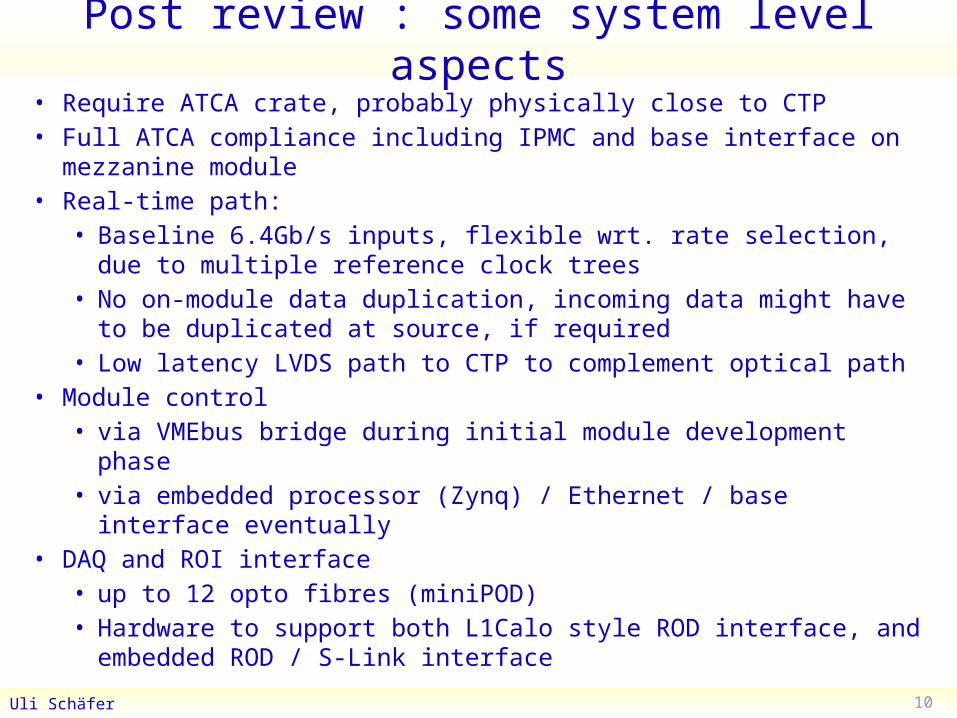
Post review : some system level aspects• Require ATCA crate, probably physically close to CTP• Full ATCA compliance including IPMC and base interface on
mezzanine module• Real-time path:
• Baseline 6.4Gb/s inputs, flexible wrt. rate selection, due to multiple reference clock trees
• No on-module data duplication, incoming data might have to be duplicated at source, if required
• Low latency LVDS path to CTP to complement optical path• Module control
• via VMEbus bridge during initial module development phase• via embedded processor (Zynq) / Ethernet / base interface
eventually • DAQ and ROI interface
• up to 12 opto fibres (miniPOD)• Hardware to support both L1Calo style ROD interface, and
embedded ROD / S-Link interfaceUli Schäfer

11
Hardware status - floor plan, so far…
Uli Schäfer
RTDP:• 48-way opto connectors• 14 miniPODs / optical in• add clock trees to
support multiple input rates
• 2 processors XC7V690T • To CTP: miniPOD and low
latency LVDSControl etc.:• XC7K325T and
XC7Z0XX• Add SD-card for
configuration and boot• Add memorySome components not yet placed : CTP / spare PODs…
12
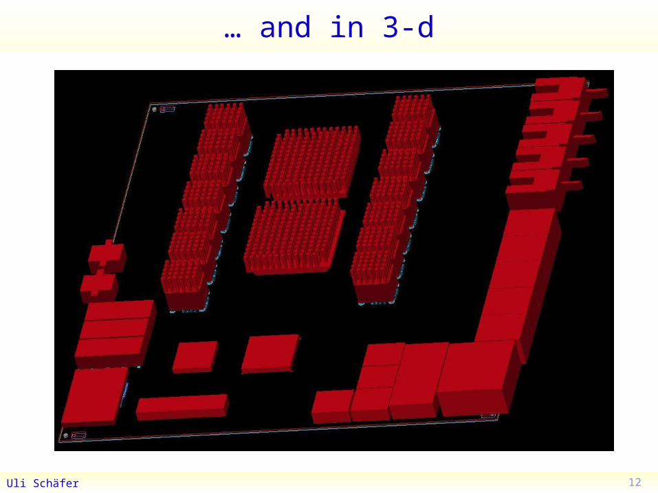
… and in 3-d
Uli Schäfer
13
Options and EffortImpact of architectural decisions (as discussed at review) on f/w and s/w:• Embedded ROD vs. use of L1Calo ROD (pre phase 1)
• Effort required for embedded ROD cannot be quantified yet• JEM (L1Calo) DAQ interface being converted to L1Topo needs (low effort)• DAQ bandwidth dominated by CMX data : Zero suppressed format @ 100kHz L1A ~1/2
L1Calo ROD channel worth of data per bunch tick being read out• Ethernet based control / embedded processor / IPbus
• Basic access via serialised VMEbus is available anyway, is in use on GOLD• “IPbus” or embedded processor supported by h/w, require s/w & f/w effort
Firmware :• Real-time code being developed on GOLD (MGT and some topo algorithms)• Register map• DAQ • Diagnostics and monitoring (playback / spy functionality) • IPbus firmware (for FPGA-based Ethernet option)
Software :• Some basic software access for h/w tests• HDMC register description (in case of register mapped access)• General software framework for Ethernet based control• (Embedded ARM/Linux or IPbus specific) and IPMC controller software
S/W development eased considerably if done within L1Calo infrastructureUli Schäfer

14
Summary
Uli Schäfer
L1Topo functional demonstrator (GOLD):• High-speed o/e data paths successfully tested• Parameters optimized at 6.4 Gb/s• Large bit-error free windows• Further optimization on high speed link parameters and
performance (latency) of algorithms in hardware on-going
L1Topo Prototype:• Design ready, reviewed, schematic capture in progress• A few post-review modifications • Some mods go onto mezzanine module• Critical components ordered / expected on time for
production• Considerable effort to go into s/w, f/w, system-level
integration• On schedule for installation during shutdown 13/14


