
LTC2937
12937fa
For more information www.linear.com/LTC2937
TYPICAL APPLICATION
FEATURES DESCRIPTION
Programmable Six Channel Sequencer and Voltage Supervisor with EEPROM
The LTC®2937 is a 6-channel power supply sequencer and voltage supervisor. Supplies are enabled or disabled with precise user controlled order and time spacing. To detect power supply output faults during sequencing and monitoring, the LTC2937 accurately monitors supply turn-on/-off delays and output voltage levels. In the event of a fault, response actions include complete power supply shutdown and optional restarts. Root cause of power faults are logged to EEPROM. For systems with high supply count, a simple single wire connection between multiple LTC2937 devices allows sequencing expansion to 300 supplies. After successful sequencing and supply voltage stabilization, the reset output pulls high to initiate microprocessor or other system activity. To accommodate supply margin testing, the reset output can be disabled. Upon supply turn-off, integrated current sources are available as needed to discharge slowly decaying supplies. Configuration EEPROM supports autonomous operation without software.
Six Power Supply Sequencer and SupervisorSequenced Power Supply Waveforms
APPLICATIONS
n Time and Event Based Sequencing n 12 Programmable Undervoltage (UV) and Overvolt-
age (OV) Comparators: ±0.75% Accuracy n I2C/SMBus Interface n Stalled Power Supply Detection n Single Wire Synchronization Allows Controller
Expansion to 50 Devices (300 Power Supplies) n Configuration and Fault Logging in EEPROM n EEPROM Specified Over Entire Temperature Range,
Rated to 125°C, 10k Writes, 20yr Retention n Supported by LTpowerPlay® GUI n Fault and System Status Registers n Reset Output with Programmable Delay n Wide Input Supply Voltage Range: 2.9V to 16.5V n 28-Lead QFN (5mm × 6mm) Package
n Network Servers n Data Storage Systems n Telecom Equipment n High Availability Computer Systems
L, LT, LTC, LTM, Linear Technology, the Linear logo, LTpowerPlay and PolyPhase are registered trademarks of Linear Technology Corporation. All other trademarks are the property of their respective owners. Protected by U.S. Patents including 8627132.
R13.3k
C12.2µF
LTC2937
SDASCLALERTB
ONMARGBFAULTBRSTB
SHARE_CLKASEL1ASEL2ASEL3WPVDD
VPWR
GND
SPCLK
I2C/SMBusINTERFACE
TO/FROMOTHER
DEVICES
EN1EN2EN3EN4EN5EN6
V1V2V3V4V5V6
2937 TA01a
OUT1RUN1RUN2RUN3RUN4RUN5RUN6
OUT2OUT3OUT4OUT5OUT6
VIN12V
GND
5.0V3.3V2.5V1.8V1.5V1.2V
DC/DCCONVERTERS
5V
3.3V
2.5V
1.8V
1.5V
1.2V
ON
TIME
V1V2V3
VOLT
AGE
V4
V5
V6
2937 TAO1b

LTC2937
22937fa
For more information www.linear.com/LTC2937
TABLE OF CONTENTSFeatures ..................................................... 1Applications ................................................ 1Typical Application ........................................ 1Description.................................................. 1Absolute Maximum Ratings .............................. 3Order Information .......................................... 3Pin Configuration .......................................... 3Electrical Characteristics ................................. 4Serial Bus Timing Diagram .............................. 7Sequence-Up Threshold Timing Diagram .............. 7Sequence-Down Event Based Timing Diagram........ 8Sequence-Down Time Based Timing Diagram ........ 9Typical Performance Characteristics .................. 10Pin Functions .............................................. 12Block Diagram ............................................. 13Operation................................................... 14
Slave Addresses ..................................................... 15I2C Interface ........................................................... 16
Condensed Command Summary ....................... 17Command Descriptions .................................. 18
WRITE_PROTECTION ............................................. 18SPECIAL_LOT ......................................................... 18ON_OFF_CONTROL ................................................. 19V_RANGE ...............................................................20V_THRESHOLD_n ................................................... 21Voltage Threshold Encoding ................................... 21TON_TIMERS_n ......................................................22TOFF_TIMERS_n .....................................................23SEQ_UP_POSITION_n ............................................ 24SEQ_DOWN_POSITION_n ......................................25RSTB_CONFIG ........................................................26FAULT_RESPONSE .................................................27MONITOR_STATUS_HISTORY ................................29CLEAR_ALERTB .....................................................30STORE ....................................................................30RESTORE ................................................................30CLEAR ....................................................................30STATUS_INFORMATION ......................................... 31BREAK_POINT ........................................................32SEQ_POSITION_COUNT .........................................32MONITOR_BACKUP ................................................33
MONITOR_STATUS ................................................34DEVICE_ID ..............................................................34
Applications Information ................................ 35Introduction ............................................................35Powering the LTC2937 ............................................35Write Protection ......................................................35Updating Volatile or Nonvolatile Memory ................35Sequence Position Clock (SPCLK) ..........................36System Configuration ............................................. 37Sequence-Up and Sequence-Down Control ............ 37Sequence-Up Parameters .......................................38Voltage Supervision ................................................38Voltage Monitor Range ...........................................38UV and OV Thresholds ............................................39UV Thresholds and Sequence-Up Hysteresis ..........39Selecting Resistors for Adjustable Range ...............39OV Thresholds in Adjustable Applications ..............40RSTB Response ...................................................... 41Sequence-Down Parameters .................................. 41Discharge Thresholds .............................................42Active Supply Discharge .........................................42Fault Descriptions ...................................................43CONTROL Faults .....................................................43SEQUENCE Faults ...................................................43SUPERVISOR Faults ...............................................43EXTERNAL Faults ...................................................43SHARE_CLK Faults .................................................43Fault Reporting .......................................................44Fault Management ..................................................44Fault Debugging Tools ............................................46Share Clock (SHARE_CLK) .....................................46Asynchronous Supply Control ................................46LTpowerPlay: An Interactive GUI for Power System Management ........................................................... 47External Connection Design Checklist .................... 47Minimum Connections for Programming ................48Interconnect Between Multiple LTC2937s ...............48System Event Based Sequencing ............................48
Package Description ..................................... 50Revision History .......................................... 51Typical Application ....................................... 52Related Parts .............................................. 52

LTC2937
32937fa
For more information www.linear.com/LTC2937
PIN CONFIGURATIONABSOLUTE MAXIMUM RATINGS
VPWR ........................................................ –0.3V to 18VEN1, EN2, EN3, EN4, EN5, EN6 .................. –0.3V to 16VVDD, ALERTB, FAULTB, MARGB, RSTB,ON, SCL, SDA, SHARE_CLK, SPCLK, WP,V1, V2, V3, V4, V5, V6 .................................. –0.3V to 6VASEL1, ASEL2, ASEL3 ............................... –0.3V to VDDInput Currents
V1, V2, V3, V4, V5, V6........................................–1mAOperating Junction Temperature Range
LTC2937C ................................................ 0°C to 70°C LTC2937I .............................................–40°C to 85°C
LTC2937H .......................................... –40°C to 125°CStorage Temperature Range .................. –65°C to 150°CMaximum Junction Temperature .......................... 130°C
(Notes 1, 2)
9 10
TOP VIEW
UHE PACKAGE28-LEAD (5mm × 6mm) PLASTIC QFN
29
11 12 13
28 27 26 25 24
14
23
6
5
4
3
2
1MARGB
VPWR
VDD
GND
ON
ASEL1
ASEL2
ASEL3
WP
SHARE_CLK
SPCLK
SCL
SDA
RSTB
FAULTB
ALERTB
V1 V2 V3 V4 V5 V6
EN1
EN2
EN3
EN4
EN5
EN6
7
17
18
19
20
21
22
16
8 15
TJMAX = 130°C, θJA = 43°C/W
EXPOSED PAD (PIN 29) PCB CONNECTION TO GND OPTIONAL
ORDER INFORMATIONLEAD FREE FINISH TAPE AND REEL PART MARKING* PACKAGE DESCRIPTION TEMPERATURE RANGE
LTC2937CUHE#PBF LTC2937CUHE#TRPBF 2937 28-Lead (5mm × 6mm) Plastic QFN 0°C to 70°C
LTC2937IUHE#PBF LTC2937IUHE#TRPBF 2937 28-Lead (5mm × 6mm) Plastic QFN –40°C to 85°C
LTC2937HUHE#PBF LTC2937HUHE#TRPBF 2937 28-Lead (5mm × 6mm) Plastic QFN –40°C to 125°C
Consult LTC Marketing for parts specified with wider operating temperature ranges. *The temperature grade is identified by a label on the shipping container. For more information on lead free part marking, go to: http://www.linear.com/leadfree/ For more information on tape and reel specifications, go to: http://www.linear.com/tapeandreel/. Some packages are available in 500 unit reels through designated sales channels with #TRMPBF suffix.
http://www.linear.com/product/LTC2937#orderinfo

LTC2937
42937fa
For more information www.linear.com/LTC2937
SYMBOL PARAMETER CONDITIONS MIN TYP MAX UNITS
Device Power
VVPWR VPWR Supply Input Operating Range l 4.5 16.5 V
IVPWR VPWR Supply Current Sequencing Complete, No VDD Load Writing to EEPROM
l
l
1 3
mA mA
VDDREG VDD Regulated Output VPWR ≥ 4.5V, IVDD = –1mA l 3.234 3.3 3.366 V
VOP VDD Operating Range VDD Connected to VPWR l 2.9 5.5 V
VUVL VDD Undervoltage Lockout VDD Rising l 2.5 2.7 2.85 V
VUVL(HYST) VDD Undervoltage Lockout Hysteresis VDD Falling 75 mV
V1, V2, V3, V4, V5, V6
VMON Vn Monitoring Thresholds (n = 1 through 6) (Note 3)
Adjustable Range Low Range High Range
l
l
l
0.2 0.5 1
1.2 3 6
V V V
VRES Vn Threshold Programming LSB Resolution
Adjustable Range Low Range High Range
4 10 20
mV mV mV
VMON(ACC) Vn Threshold Accuracy by Code (Note 4)
C-, I-Grades: Codes 155 to 255 Codes 55 to 154 Codes 5 to 54 H-Grade: Codes 155 to 255 Codes 55 to 154 Codes 5 to 54
l
l
l
l
l
l
±0.75 ±0.75 ±1.5
±1 ±1
±1.5
% % %
% % %
VMON(HYST) Temporary Sequence-Up Threshold Hysteresis (Note 5)
Sequence Up Threshold Achieved l –4 –5 –6 %
tPD Vn Comparator Propagation Delay 2 LSB Overdrive of Configured Threshold 10 LSB Overdrive of Configured Threshold
l
35 10
25
µs µs
RIN Vn Input Resistance Low Range and High Range l 400 600 900 kΩ
ILKG Vn Input Leakage Current Adjustable Range, V = 1.2V l ±15 nA
RON Vn Discharge On Resistance V = 0.4V l 25 40 50 Ω
IAD(MAX) Vn Discharge Current V = 1.8V l 20 35 45 mA
VDTH Vn Discharge Threshold High and Low Range Adjustable Range (Positive Polarity) Adjustable Range (Negative Polarity)
l
l
l
300 50
1.12
400 120 1.2
500 190 1.28
mV mV
V
EEPROM
Retention (Notes 6, 7) l 20 Years
Endurance 1 Cycle = 1 STORE Command (Notes 6, 7) l 10,000 Cycles
tPT Programming Time (Note 8) STORE Command l 130 ms
tRT Restore Time RESTORE Command l 2 ms
RSTB
tRST Programmable Reset Delay (Register 0x22, RSTB_CONFIG)
b[15:13] = 000b b[15:13] = 001b b[15:13] = 010b b[15:13] = 011b b[15:13] = 100b b[15:13] = 101b b[15:13] = 110b b[15:13] = 111b
l
l
l
l
l
l
l
l
0 1.4 5.8 22 46
180 370
1480
0.05 1.6 6.4 26 51
200 410
1640
0.1 1.9 7.5 30 60
230 475
1900
ms ms ms ms ms ms ms ms
ELECTRICAL CHARACTERISTICS The l denotes the specifications which apply over the full operating temperature range, otherwise specifications are at TA = 25°C and VPWR = 12V. (Note 2)

LTC2937
52937fa
For more information www.linear.com/LTC2937
SYMBOL PARAMETER CONDITIONS MIN TYP MAX UNITS
Sequence Timers
tON_MAX ton_max time (Registers 0x0A through 0x0F)
b[15:13] = 000b b[15:13] = 001b b[15:13] = 010b b[15:13] = 011b b[15:13] = 100b b[15:13] = 101b b[15:13] = 110b b[15:13] = 111b
l
l
l
l
l
l
l
l
∞ 136 540 2.2 8.7 35
140 560
∞ 160 640 2.6
10.2 41
164 655
∞ 195 780 3.2
12.4 50
200 800
s µs µs
ms ms ms ms ms
tOND ton_delay Time (Registers 0x0A through 0x0F)
Timer Register Value N = b[12:0] l 68 • N 80 • N 96 • N µs
tOFF_MAX toff_max Time (Registers 0x10 through 0x15)
b[15:13] = 000b b[15:13] = 001b b[15:13] = 010b b[15:13] = 011b b[15:13] = 100b b[15:13] = 101b b[15:13] = 110b b[15:13] = 111b
l
l
l
l
l
l
l
l
∞ 2.2 8.7 35
140 560 2.3 9
∞ 2.6
10.2 41
164 655 2.6
10.5
∞ 3.2
12.4 50
200 800 3.2 13
s ms ms ms ms ms
s s
tOFFD toff_delay Time (Registers 0x10 through 0x15)
Timer Register Value N = b[12:0] l 68 • N 80 • N 96 • N µs
SPCLK
tONSQ ON Input to Start of SPCLK (Note 9) l 40 80 120 µs
IPU SPCLK Pull-Up Current VSPCLK = GND l –30 –55 –80 µA
tLO Minimum SPCLK Low Time l 16 20 26 µs
tHI Minimum SPCLK High Time l 48 60 75 µs
tFLOAT SPCLK Float High Time End of Sequencing l 260 320 400 µs
SHARE_CLK
fSHR Share Clock Frequency l 85 100 110 kHz
Analog and Digital I/O
VTH Input Threshold: ON, MARGB, WP, RSTB, FAULTB, SHARE_CLK, SPCLK
l 1 1.2 1.4 V
VTH(HYST) Input Threshold Hysteresis: ON, MARGB, WP, RSTB, FAULTB, SHARE_CLK, SPCLK
50 mV
VOL Voltage Output Low: ALERTB, RSTB, FAULTB, SHARE_CLK, SPCLK, EN1, EN2, EN3, EN4, EN5, EN6
ISINK = 3mA l 0.2 0.4 V
IPU Internal Pull-Up Current: ON, MARGB, WP, ALERTB, RSTB, FAULTB
V = GND l –4 –10 –16 µA
ELECTRICAL CHARACTERISTICS The l denotes the specifications which apply over the full operating temperature range, otherwise specifications are at TA = 25°C and VPWR = 12V. (Note 2)

LTC2937
62937fa
For more information www.linear.com/LTC2937
Note 1: Stresses beyond those listed under Absolute Maximum Ratings may cause permanent damage to the device. Exposure to any Absolute Maximum Rating condition for extended periods may affect device reliability and lifetime.Note 2: All currents into device pins are positive. All currents out of device pins are negative. All voltages are referenced to GND unless otherwise specified.Note 3: Subscript (or placeholder) n denotes a channel number and is applied throughout this document.Note 4: Threshold codes 0 through 4 are not used.Note 5: During sequence-up operation, undervoltage comparators participating in sequencing receive a temporary 5% hysteresis after the respective monitored voltage exceeds its threshold for the first time. The hysteresis remains active until 50% of the programmed reset delay time
has been completed. See the timing diagram and applications information for more details.Note 6: EEPROM endurance and retention are guaranteed by design, characterization and correlation with statistical process controls.Note 7: EEPROM endurance and retention will be degraded when TJ > 85°C.Note 8: The LTC2937 will not acknowledge any commands while a STORE command is being executed.Note 9: If multiple LTC2937s are in use, tONSQ can stretch indefinitely until all devices are ready to sequence.Note 10: Maximum capacitive load, CB, for SCL and SDA is 400pF. Data and clock rise time (tr) and fall time (tf) are: (20 + 0.1 • CB) (ns) < tr < 300ns and (20 + 0.1 • CB) (ns) < tf < 300ns. CB = capacitance of one bus line in pF. SCL and SDA external pull-up voltage, VIO, is 2.9V < VIO < 5.5V.
SYMBOL PARAMETER CONDITIONS MIN TYP MAX UNITS
Leakage Current: ALERTB, RSTB, FAULTB Leakage Current: EN1, EN2, EN3, EN4, EN5, EN6
V = 5.5V V = 15V
l
l
±1 ±1
µA µA
VOH Voltage Output High: ALERTB, RSTB, FAULTB
ISOURCE = –1μA l VDD – 1 V
tPW Minimum Detectable Pulse Width: ON, FAULTB
l 25 µs
Serial Bus Interface and Address Inputs
VASEL(H) ASEL Input High Threshold l VDD – 0.4 V
VASEL(L) ASEL Input Low Threshold l 0.4 V
VASEL(OC) ASEL Open Circuit Voltage 0.5 • VDD V
VASEL(OCR) ASEL Allowable Open Circuit Voltage Range
l 0.4 • VDD 0.6 • VDD V
IASEL(HZ) Allowable Leakage in Open State l ±1 µA
ASEL Input Resistance l 120 180 280 kΩ
VSTH SDA, SCL Input Threshold l 1.5 1.8 2 V
ISTH SDA, SCL Input Current SDA or SCL = 5.5V l 0 ±2 µA
VSDA(OL) SDA Output Low Voltage ISDA = 3mA l 0.3 0.4 V
Serial Bus Timing (Note 10)
fSCL(MIN) Minimum Serial Clock Frequency l 10 kHz
fSCL(MAX) Maximum Serial Clock Frequency l 400 kHz
tLOW(MIN) Serial Clock Low Period l 1.3 µs
tHIGH(MIN) Serial Clock High Period l 0.6 µs
tBUF(MIN) Bus Free Time Between Stop and Start l 1.3 µs
tHD,STA(MIN) Start Condition Hold Time l 600 ns
tSU,STA(MIN) Start Condition Setup Time l 600 ns
tSU,STO(MIN) Stop Condition Setup Time l 600 ns
tHD,DAT(MIN) Data Hold Time (LTC2937 Receiving Data) l 0 ns
tHD,DAT Data Hold Time (LTC2937 Transmitting Data) l 300 900 ns
tSU,DAT(MIN) Data Setup Time l 100 ns
ELECTRICAL CHARACTERISTICS The l denotes the specifications which apply over the full operating temperature range, otherwise specifications are at TA = 25°C and VPWR = 12V. (Note 2)

LTC2937
72937fa
For more information www.linear.com/LTC2937
SERIAL BUS TIMING DIAGRAM
SEQUENCE-UP THRESHOLD TIMING DIAGRAM
2937 TD1
SDA
SCL
tf tr tf tBUFtLOW tSU:DAT tHD:STA tSP
tf
tHD:DAT tHIGH
tHD:STA tSU:STA tSU:STOS P SSr
ON IGNORED
VDD
SPCLK
EN1
V1
RSTB
EN2
V1MON(UV)V1MON(HYST)
V2MON(UV)V2MON(HYST)
V20.5 • tRST
tRST
tFLOAT
tLOtHItONSQ
tRT
2937 TD02
Sequencing 2 Channels (V1, V2), Both Combined into RSTB Logic

LTC2937
82937fa
For more information www.linear.com/LTC2937
SEQUENCE-DOWN EVENT BASED TIMING DIAGRAM
Sequencing 2 Channels (V1, V2), Both Combined into RSTB Logic
ON
SPCLK
EN1
V1
RSTB
tONSQ tHI tLO
EN2
V1MON(UV)
V2
tFLOAT
V1DTH
V2DTH
2937 TD03

LTC2937
92937fa
For more information www.linear.com/LTC2937
SEQUENCE-DOWN TIME BASED TIMING DIAGRAM
Sequencing 2 Channels (V1, V2), Both Combined into RSTB Logic. toff_max Timers Used for Post Disable Sequencing Delay; ON_OFF_CONTROL b[0] = 1
ON
SPCLK
EN1
V1
RSTB
EN2
V1MON(UV)
toff_max_1
toff_max_2
2937 TD04
tONSQ tHI tLOtFLOAT

LTC2937
102937fa
For more information www.linear.com/LTC2937
VOP (V)2.5 3 3.5 4 4.5 5 5.5 6
300
400
500
600
700
800
900
1000
I VPW
R +
I VDD
(µA)
2937 G02
125°C 25°C–40°C
VVPWR (V)4 6 8 10 12 14 16 18
3.24
3.26
3.28
3.30
3.32
3.34
3.36
VDD R
EG (V
)
2937 G03
125°C 25°C–40°C
TYPICAL PERFORMANCE CHARACTERISTICS
VDD Load RegulationVDD Load Step Transient Response
Comparator Threshold Accuracy vs Temperature
Comparator Glitch Immunity Timer Variation vs Temperature Timer Line Regulation
VPWR Input Current(Regulated VDD)
Input Current(VDD tied to VPWR) VDD Line Regulation
VVPWR (V)4 6 8 10 12 14 16 18
300
400
500
600
700
800
900
1000
I VPW
R (µ
A)
2937 G01
125°C 25°C–40°C
IVDD (mA)–5–4–3–2–10
3.24
3.26
3.28
3.30
3.32
3.34
3.36
2937 G04
VDD R
EG (V
)
125°C 25°C–40°C
50ms/DIV
LOAD STEP2mA/DIV
VDD50mV/DIV
2937 G05
THRESHOLD OVERDRIVE (LSBs)1 10 100
0
5
10
15
20
25
30
35
40
GLIT
CH D
URAT
ION
(µs)
2937 G07
GLITCHES ABOVE CURVEARE DETECTED
GLITCHES BELOWCURVE ARE IGNORED
VOP (V)2.5 3 3.5 4 4.5 5 5.5 6
–15
–10
–5
0
5
10
15
TIM
ER V
ARIA
TION
(%)
2937 G09
ton_max, ton_delay, toff_max, toff_delay
TEMPERATURE (°C)–50 –25 0 25 50 75 100 125
–1
–0.75
–0.5
–0.25
0
0.25
0.5
0.75
1
V MON
(ACC
) (%
)
vs Temperature
2937 G06
TEMPERATURE (°C)–50 –25 0 25 50 75 100 125
–15
–10
–5
0
5
10
15
TIM
ER V
ARIA
TION
(%)
Timer Variation vs Temperature
2937 G08

LTC2937
112937fa
For more information www.linear.com/LTC2937
TYPICAL PERFORMANCE CHARACTERISTICS
SHARE_CLK Frequency vs Temperature
SHARE_CLK Frequency Line Regulation
Reset Delay Variation vs Temperature
Active Discharge Current vs Monitor Input Voltage
Discharge Threshold Variation vs Temperature RSTB (Low) vs VDD
VOL vs Output Sink CurrentRSTB, FAULTB, ALERTB ENn VOL vs Output Sink Current ASELn Current vs Input Voltage
CURRENT (mA)0 2 4 6 8 10
0
0.2
0.4
0.6
0.8
1
V OL
(V)
2937 G10
125°C 25°C–40°C
VOP (V)2.5 3 3.5 4 4.5 5 5.5 6
–10
–5
0
5
10
FREQ
UENC
Y VA
RIAT
ION
(%)
2937 G14
VMON (V)0 1 2 3 4 5 6
0
5
10
15
20
25
30
35
40
I AD
(mA)
2937 G16
125°C 25°C–40°C
10k PULL-UP FROM VDD TO RSTB
VDD (V)0 0.5 1 1.5 2 2.5 3
0
0.2
0.4
0.6
0.8
1
RSTB
(V)
2937 G18
CURRENT (mA)0 2 4 6 8 10
0
0.2
0.4
0.6
0.8
1
V OL
(V)
2937 G11
125°C 25°C–40°C
VASEL (V)0 1 2 3 4 5
–20
–10
0
10
20
CURR
ENT
(µA)
2937 G12
VDD = 5VVDD = 3.3V
TEMPERATURE (°C)–50 –25 0 25 50 75 100 125
90
92
94
96
98
100
102
104
106
108
110
FREQ
UENC
Y (H
z)
vs Temperature
2937 G13
TEMPERATURE (°C)–50 –25 0 25 50 75 100 125
–15
–10
–5
0
5
10
15
RESE
T DE
LAY
VARI
ATIO
N (%
)
vs Temperature
2937 G15
TEMPERATURE (°C)–50 –25 0 25 50 75 100 125
–15
–10
–5
0
5
10
15
V DTH
VAR
IATI
ON (%
)
vs Temperature
2937 G17

LTC2937
122937fa
For more information www.linear.com/LTC2937
PIN FUNCTIONSALERTB: Alert Open-Drain Output with 10µA Pull-Up to VDD. Asserts low in response to any designated fault. Conforms to SMBus standard. Apply the Alert Response Protocol to clear the ALERTB output and to identify the alerting device. Performing a read from the CLEAR_ALERTB register will also remove ALERTB pull-down.
ASEL1, ASEL2, ASEL3: Three-State Address-Select Inputs. Connect to GND, VDD or open to encode 1 of 27 device addresses. Consult the Operation section for the address look-up table.
EN1, EN2, EN3, EN4, EN5, EN6: Power Supply Enable Outputs. Connect these open-drain outputs to a respective power supply enable input or to a gate of an N-channel MOSFET (for pass applications). The enable outputs must be pulled up externally (to a maximum of 15V) if necessary. Some power supply enable inputs have internal pull-up sources, which eliminates the need for an external pull-up.
Exposed Pad: Leave open or connect to device GND.
FAULTB: Fault I/O with 10µA Pull-Up to VDD. Asserts low in response to any designated fault. Configure fault behavior in the FAULT_RESPONSE register. External devices may also pull down on FAULTB to initiate an optional fault response.
GND: Device Ground.
MARGB: Margin Input. Pull to ground to disable RSTB and prevent SUPERVISOR faults. Typically applied prior to margining supplies high or low during system test. Leave open or pull to VDD when not margining.
ON: Sequencing Up/Down Control Input. ON input response is gated by settings in the ON_OFF_CONTROL register. Internally pulled up to VDD with 10µA current source.
RSTB: Reset I/O with 10µA Pull-Up to VDD. Pulls low in response to designated voltage comparator violations. Pulls high when selected voltage sense thresholds are satisfied (ie not UV and/or not OV), and can be used as a system power-on-reset. The reset assertion delay after satisfying thresholds is programmable. May be pulled low by external devices and detected with b[12] of the MONITOR_STATUS command.
SCL: Serial Clock Input (400kHz Maximum). Requires external pull-up resistor.
SDA: Bidirectional Serial Data I/O. Requires external pull-up resistor.
SHARE_CLK: Clock Sharing Node. Connect multiple SHARE_CLK nodes together to establish a common time base between devices. Pull-up with a 3.3k to 10k resistor to VDD.
SPCLK: Sequence Position Clock I/O. Connect multiple LTC2937 SPCLK lines together for automatic sequence position control between devices. Pull-up devices are not recommended. Leave unconnected in a single device application. Minimize capacitance on this line to ensure reliable operation.
V1, V2, V3, V4, V5, V6: Undervoltage, Overvoltage and Discharge Comparator Inputs. There are three sense ranges. Adjustable: 0.2V to 1.2V in 4mV increments, Low: 0.5V to 3V in 10mV increments, and High: 1V to 6V in 20mV increments. When monitored supplies are shut off, internal pull-down current sources can be activated to accelerate the discharge of supply capacitance. Connect to device GND if unused.
VDD: 3.3V Internal Regulator Output. Bypass with a 2.2µF (or greater) capacitor to GND. Use this output to bias the address inputs or an external resistor network for sensing negative supply voltages. Do not load the regulated output with more than 5mA. Override the regulated output with an external supply (2.9V to 5.5V) connected to VPWR and VDD.
VPWR: Supply Voltage Input. Power supply operating range is 4.5V to 16.5V. Tie to VDD if unused. Bypass with 0.1µF (or greater) capacitor to GND.
WP: Write Protection Input. Pull to GND to enable write capability into the device. Leave open or tie to VDD to keep write protection active. The software controlled lock bit in the WRITE_PROTECTION register may also need deactivation to enable write capability.

LTC2937
132937fa
For more information www.linear.com/LTC2937
BLOCK DIAGRAM
–
+
EN6
RSTB10µAREF
DISCH
LOGIC
VDD
EN5
EN4
EN3
EN2
EN1
FAULTB10µA
VDD
ALERTB10µA
VDD
SPCLK
SCL
SDA
ASEL1
ASEL2
ASEL3
50µA
VDD
10µA
VDD
SHARE_CLK
SERIALPORT
INTERFACE
UVLO
OSC
LDO
EEPROMAND
REGISTERS
VPWR
VDD
V1
VDD
MARGB
10µA
VDDWP
10µA
VDDON
ADJPOL
ADJPOL
CHANNEL 1
30mA
V2
GND
CHANNEL 2
V3CHANNEL 3
V4CHANNEL 4
V5CHANNEL 5
V6CHANNEL 6
VDD
–
+OV
–
+UV

LTC2937
142937fa
For more information www.linear.com/LTC2937
OPERATIONThe LTC2937 is a six-channel programmable power supply sequencer and supervisor that can perform the following operations:
• Control the timing relationships and sequence order for six power supplies per device. Sequence supplies on the basis of time delays and/or qualifying events.
• Monitor power supplies for undervoltage (UV) and overvoltage (OV) conditions using two independent comparators on each of six inputs.
• Generate a system reset that is a function of user selected inputs with a programmable release delay.
• Synchronize sequencing across multiple controllers with a one wire connection (SPCLK).
• Synchronize timing across multiple controllers with a one wire connection (SHARE_CLK).
• Discharge slowly decaying supplies with built-in pull-down current sources.
• Monitor power supplies for discharge condition using the discharge comparators.
• Accept I2C/SMBus programming commands.
• Initiate supply sequencing from an external source and/or programming command.
• Retrieve real-time system status.
• Generate a fault related interrupt on the ALERTB output and respond to an issued SMBus Alert Response.
• Respond to fault conditions by continuing operation indefinitely or disabling supplies immediately. Optionally, sequencing may be retried multiple times automatically (0 to 6 or unlimited) after a supply shutdown event.
• Report voltage and/or timing limit violations upon request.
• Pause sequencing operations to help identify system power problems.
• Store system configuration to EEPROM.
• Restore EEPROM contents to operating memory through programming or when VDD is applied on power-up.
• Recall first fault violations logged to EEPROM.
• EEPROM reads and writes over the entire specified supply voltage and temperature range.
• Provide two stage write protection to prevent inad-vertent writes to memory.
• Disable system reset when performing voltage margining of supplies.
• Monitor negative power supplies.

LTC2937
152937fa
For more information www.linear.com/LTC2937
OPERATION
Table 1. LTC2937 Address Look-Up TableDESCRIPTION HEX DEVICE ADDRESS BINARY DEVICE ADDRESS ADDRESS INPUTS
7-Bit 8-Bit 6 5 4 3 2 1 0 R/W ASEL3 ASEL2 ASEL1
Alert Response 0C 19 0 0 0 1 1 0 0 1 X X X
Global 36 6C 0 1 1 0 1 1 0 0 X X X
37 6E 0 1 1 0 1 1 1 X L L L
38 70 0 1 1 1 0 0 0 X L L NC
39 72 0 1 1 1 0 0 1 X L L H
3A 74 0 1 1 1 0 1 0 X L NC L
3B 76 0 1 1 1 0 1 1 X L NC NC
3C 78 0 1 1 1 1 0 0 X L NC H
3D 7A 0 1 1 1 1 0 1 X L H L
3E 7C 0 1 1 1 1 1 0 X L H NC
3F 7E 0 1 1 1 1 1 1 X L H H
40 80 1 0 0 0 0 0 0 X NC L L
41 82 1 0 0 0 0 0 1 X NC L NC
42 84 1 0 0 0 0 1 0 X NC L H
43 86 1 0 0 0 0 1 1 X NC NC L
44 88 1 0 0 0 1 0 0 X NC NC NC
45 8A 1 0 0 0 1 0 1 X NC NC H
46 8C 1 0 0 0 1 1 0 X NC H L
47 8E 1 0 0 0 1 1 1 X NC H NC
48 90 1 0 0 1 0 0 0 X NC H H
49 92 1 0 0 1 0 0 1 X H L L
4A 94 1 0 0 1 0 1 0 X H L NC
4B 96 1 0 0 1 0 1 1 X H L H
4C 98 1 0 0 1 1 0 0 X H NC L
4D 9A 1 0 0 1 1 0 1 X H NC NC
4E 9C 1 0 0 1 1 1 0 X H NC H
4F 9E 1 0 0 1 1 1 1 X H H L
50 A0 1 0 1 0 0 0 0 X H H NC
51 A2 1 0 1 0 0 0 1 X H H H
H = Tie to VDD, L = Tie to GND, NC = No Connect = Open, X = Don’t Care
Slave Addresses
The LTC2937 responds to one of 27 addresses. Connect the ASEL1, ASEL2 and ASEL3 inputs to VDD, GND, or leave open, as shown in Table 1. The LTC2937 always responds to the Global and Alert Response addresses regardless of the ASEL input states. The ASEL inputs are always active and operate in real time.

LTC2937
162937fa
For more information www.linear.com/LTC2937
OPERATION
SLAVE ADDRESS COMMAND CODE DATA BYTE LOWWr A A A P2937 F03
S
7 8 8 1
DATA BYTE HIGH
81 1 1 1 11
A
SLAVE ADDRESS COMMAND CODE SLAVE ADDRESSWr A A A P2937 F04
S
7 8 7 1
DATA BYTE LOW
8
DATA BYTE HIGH
811 1 1
Sr
1 1 11
A
1
Rd A
SLAVE ADDRESS Rd A A
0001100
P2937 F05
S
7 81 1 1 11
DEVICE ADDRESS
Figure 2. Send Byte Protocol
Figure 3. Write Word Protocol
Figure 4. Read Word Protocol
Figure 5. Alert Response Protocol
Figure 1. Serial Bus Protocol Diagram Element Key
SLAVE ADDRESS Wr A A P2937 F02
S
7 81 1 1 11
COMMAND CODE
2937 F01
S START CONDITION
Sr REPEATED START CONDITION
Rd READ (BIT VALUE OF 1)
Wr WRITE (BIT VALUE OF 0)
x SHOWN UNDER A FIELD INDICATES THAT THAT FIELD IS REQUIRED TO HAVE THE VALUE OF x
A ACKNOWLEDGE
A NOT ACKNOWLEDGE
P STOP CONDITION
MASTER TO SLAVE
SLAVE TO MASTER
I2C Interface

LTC2937
172937fa
For more information www.linear.com/LTC2937
CONDENSED COMMAND SUMMARYON/OFF Commands
COMMAND NAME CMD CODE DESCRIPTIONTYPE
(Note 11)
WORD LENGTH (BITS)
EEPROM CAPACITY
(BITS)REF
PAGE
ON_OFF_CONTROL 0x02 ON input and/or I2C directed sequence up/down control settings. R/W 16 16 19
Sequencing-Up Configuration Commands
SEQ_UP_POSITION_n 0x16 – 0x1B Sequence-up position for EN1 through EN6. Asynchronous enable controls.
R/W 16 16 24
TON_TIMERS_n 0x0A – 0x0F Encode ENn delay time and maximum rise time for Vn. R/W 16 16 22
Voltage Supervisor Commands
V_RANGE 0x03 Encode Vn comparator ranges and Adjustable Range polarity. R/W 16 16 20
V_THRESHOLD_n 0x04 – 0x09 Encode high and low thresholds for Vn. R/W 16 16 21
RSTB_CONFIG 0x22 Select comparator outputs for combination into RSTB response. Select RSTB assertion delay.
R/W 16 16 26
Sequencing-Down Configuration Commands
SEQ_DOWN_POSITION_n 0x1C – 0x21 Sequence-down position for EN1 through EN6. Active discharge select for V1 through V6.
R/W 16 16 25
TOFF_TIMERS_n 0x10 – 0x15 Encode ENn delay time and maximum fall time for Vn. R/W 16 16 23
Fault, Status and Debugging Commands
FAULT_RESPONSE 0x23 Configure fault response actions. R/W 16 16 27
STATUS_INFORMATION 0x29 Summary of current device faults and status. R 16 0 31
MONITOR_STATUS_HISTORY
0x26 History of voltage monitor violations, SUPERVISOR faults and SEQUENCE faults.
R 16 0 29
MONITOR_BACKUP 0x2F An EEPROM copy of the MONITOR_STATUS_HISTORY word after the first SUPERVISOR or SEQUENCE fault.
R 16 16 33
MONITOR_STATUS 0x30 Live voltage monitor and RSTB status. R 16 0 34
SEQ_POSITION_COUNT 0x2B Sequence position counter. R 16 0 32
BREAK_POINT 0x2A Enable and configure sequencing break points. R/W 16 0 32
CLEAR 0x2E Clear all status, fault and volatile history information. S 0 0 30
CLEAR_ALERTB 0x28 Clear the ALERTB output by performing a read from this command address. The returned word contains no information.
R 16 0 30
Security and Device Information Commands
WRITE_PROTECTION 0x00 Contains lock key code and software lock bit to prevent accidental overwrites of volatile and nonvolatile memory. Status of WP input.
R/W 16 16 18
STORE 0x2C Store device configuration to EEPROM. S 0 0 30
RESTORE 0x2D Restore device configuration from EEPROM. S 0 0 30
SPECIAL_LOT 0x01 Contains customer specific codes that identify the factory programmed configuration stored in EEPROM. Use as a scratchpad if customer codes are not applied.
R/W 16 16 18
DEVICE_ID 0x31 Read only. Contains 0x2937. R 16 0 34
Note 11: R = read, W = write, S = send byte.

LTC2937
182937fa
For more information www.linear.com/LTC2937
COMMAND DESCRIPTIONSWRITE_PROTECTION(Command Byte 0x00)
Prevent write operations into EEPROM or volatile memory with the software lock bit b[0] = 1 and/or hardware lock bit b[1] = 1. Deactivate the software lock bit by matching the device key string in b[15:2] while b[1:0] = 00b. Retrieve the state of the external hardware lock input (WP) in b[1]. Improve write security by having at least one bit in the device key set to logic 1. Change the device key if desired, when the device is unlocked.
The contents of any supported command may be read regardless of the lock bit settings. Commands are acknowledged under write protection. However, the device configuration will not change.
WRITE_PROTECTION Data ContentsBIT(S) SYMBOL OPERATION
b[15:2] device_key Must match against programmed string in order to deactivate software write lock (default = 0x0EAA).
b[1] hw_lock_bit WP input status. 0: Unlocked. 1: Locked.
b[0] sw_lock_bit Software lock bit. 0: Unlocked. 1: Locked (default).
SPECIAL_LOT(Command Byte 0x01)
Read the SPECIAL_LOT register to retrieve a customer specific code that identifies the factory programmed configuration stored in EEPROM. Use as a scratchpad if customer codes are not applied. Contact LTC Marketing to request a custom factory programmed configuration and special lot number. The default value is 0x0000.

LTC2937
192937fa
For more information www.linear.com/LTC2937
ON_OFF_CONTROL(Command Byte 0x02)
Configure the combination of ON input and/or I2C inputs needed to control sequencing. Activate margin mode operation using b[6] or the external MARGB input. Specify time or event based sequence-down qualification. Prevent sequence-up initiation if supplies selected for sequencing are not discharged.
ON_OFF_CONTROL Data ContentsBIT(S) SYMBOL OPERATION
b[15:8] reserved Ignore.
b[7] on_state Internal ON status. Representation of the ON input logically modified by the b[5:1] directives below and/or freeze mode bit b[8] from FAULT_RESPONSE (read only). 0: Internal ON is low. 1: Internal ON is high.
b[6] i2c_margin RSTB disable used during supply margining. 0: RSTB operates normally (default). 1: RSTB is allowed to pull high.
b[5] discharge_start Sequenced supply discharge threshold qualification. 0: Discharged supplies not required to start sequence-up (default). 1: Discharged supplies required to start sequence-up.
b[4] i2c_on_off Serial bus directed sequence on/off control. 0: Sequence down (default). 1: Sequence up.
b[3] i2c_on_off_mask Serial bus on/off control mask. 0: Ignore b[4]. If b[3] and b[2] are low, device is in sequence down state (default). 1: Listen to b[4]. If b[2] is high, the ON input is also required to initiate sequencing.
b[2] on_input_mask ON input mask. 0: Ignore the ON input. Sequencing control directed by b[4] if not masked (default). 1: Listen to ON input.
b[1] on_polarity Invert ON input logical state. Changing polarity should be performed with b[2] low because the response is immediate and could initiate a sequencing event. 0: Sequence up with ON input at logic high (default). 1: Sequence up with ON input at logic low.
b[0] seq_down_qual Select time or event based sequence down. 0: Event based. Sequence position clock (SPCLK) advances when supplies drop below their discharge threshold (default). 1: Time based. Sequence position clock (SPCLK) advances when respective toff_max time has elapsed, including any preceding toff_delay time (if timer set to infinity, operation defaults to voltage decay mode).
COMMAND DESCRIPTIONS

LTC2937
202937fa
For more information www.linear.com/LTC2937
COMMAND DESCRIPTIONSV_RANGE(Command Byte 0x03)
Select the operating threshold range for each of the six voltage monitor inputs. The range selection applies to the OV and UV comparators connected to each input. The High Range covers thresholds between 1V and 6V in 20mV steps. The Low Range covers thresholds between 0.5V and 3V in 10mV steps. The Adjustable Range covers 0.2V to 1.2V in 4mV steps. Select the negative polarity option in the Adjustable Range when sensing negative voltages. Discharge comparator threshold and polarity adjusts automatically in response to the configured range selection.
V_RANGE Data ContentsBIT(S) SYMBOL OPERATION
b[15:12] reserved Ignore.
b[11:10] v6_range Select V6 range. 00b: High Range (default). 01b: Low Range. 10b: Adjustable Range (positive polarity). 11b: Adjustable Range (negative polarity).
b[9:8] v5_range Select V5 range. 00b: High Range (default). 01b: Low Range. 10b: Adjustable Range (positive polarity). 11b: Adjustable Range (negative polarity).
b[7:6] v4_range Select V4 range. 00b: High Range. 01b: Low Range (default). 10b: Adjustable Range (positive polarity). 11b: Adjustable Range (negative polarity).
b[5:4] v3_range Select V3 range. 00b: High Range. 01b: Low Range (default). 10b: Adjustable Range (positive polarity). 11b: Adjustable Range (negative polarity).
b[3:2] v2_range Select V2 range. 00b: High Range. 01b: Low Range (default). 10b: Adjustable Range (positive polarity). 11b: Adjustable Range (negative polarity).
b[1:0] v1_range Select V1 range. 00b: High Range. 01b: Low Range (default). 10b: Adjustable Range (positive polarity). 11b: Adjustable Range (negative polarity).

LTC2937
212937fa
For more information www.linear.com/LTC2937
COMMAND DESCRIPTIONSV_THRESHOLD_n
n 1 2 3 4 5 6
Command Byte 0x04 0x05 0x06 0x07 0x08 0x09
Program the OV and UV thresholds for each of the six voltage monitor inputs.
V_THRESHOLD_n Data ContentsBIT(S) SYMBOL OPERATION
b[15:8] ov_threshold_n Encode one of 250 thresholds (0x05 through 0xFF). See below for voltage threshold encoding (TE) procedure.
b[7:0] uv_threshold_n Encode one of 250 thresholds (0x05 through 0xFF). See below for voltage threshold encoding (TE) procedure.
Voltage Threshold Encoding
Depending on the selected voltage range, threshold encoding (TE) is determined as follows:
For the high input range of 1V to 6V, the equation is:
TE = ROUND[50 • (VMON – 0.9)]
For the low input range of 0.5V to 3V, the equation is:
TE = ROUND[100 • (VMON – 0.45)]
For the high impedance adjustable input range of 0.2V to 1.2V, the equation is:
TE = ROUND[250 • (VMON – 0.18)]
As an example, consider the channel 1 Low Range defaults from the table below (ov_threshold_1 = 1.32V, uv_threshold_1 = 1.08V). The threshold encodings (TE) are therefore:
TEOV = ROUND[100 • (1.32 – 0.45)] = ROUND[100 • (0.87)] = 87 (0x57)
TEUV = ROUND[100 • (1.08 – 0.45)] = ROUND[100 • (0.63)] = 63 (0x3F)
The16-bit word contained in the V_THRESHOLD_1 register (0x573F) is formed from the simple concatenation of the OV and UV hexadecimal values.
Factory Defaultsn RANGE VMON(OV) VMON(UV) TEOV TEUV
1 Low 1.32 V 1.08 V 0x57 0x3F
2 Low 1.65 V 1.35 V 0x78 0x5A
3 Low 1.98 V 1.62 V 0x99 0x75
4 Low 2.75 V 2.25 V 0xE6 0xB4
5 High 3.63 V 2.97 V 0x89 0x68
6 High 5.5 V 4.5V 0xE6 0xB4
(Note 3)

LTC2937
222937fa
For more information www.linear.com/LTC2937
COMMAND DESCRIPTIONS (Note 3)
TON_TIMERS_n
n 1 2 3 4 5 6
Command Byte 0x0A 0x0B 0x0C 0x0D 0x0E 0x0F
The TON_TIMER registers encode the enable delay time and the maximum allowable rise time per channel in one 16-bit word. The lowest thirteen bits (ton_delay) determine the amount time delay between the beginning of the programmed sequence position (determined by the SEQ_UP_POSITION_n command) and the release of the respective ENn output (in 80µs increments).
The upper three bits (ton_max) determine the amount of time that is allowed to elapse between the release of ENn and the voltage at the respective Vn input reaching its UV threshold. Failing this test can cause a sequence-up fault depending on the FAULT_RESPONSE settings. A setting of ∞ defeats time checking during the sequence-up phase for the respective channel (sequencing will pause indefinitely until the UV threshold is crossed).
TON_TIMERS_n Data ContentsBIT(S) SYMBOL OPERATION
b[15:13] ton_max_n Maximum rise time selection. Defined as the maximum time allowed between ENn release and successful crossing of UV threshold at the Vn input.
b[15:13] ton_max
000b ∞ (default)
001b 160µs
010b 640µs
011b 2.6ms
100b 10.2ms
101b 41ms
110b 164ms
111b 655ms
b[12:0] ton_delay_n Time delay from start of selected sequence position to enable (ENn) release. ton_delay = 80 • N µs, where N is a 13-bit unsigned integer in b[12:0]. Delay range is from 0ms to 655ms. The default setting for b[12:0] = 0.

LTC2937
232937fa
For more information www.linear.com/LTC2937
COMMAND DESCRIPTIONS (Note 3)
TOFF_TIMERS_n
n 1 2 3 4 5 6
Command Byte 0x10 0x11 0x12 0x13 0x14 0x15
The TOFF_TIMER registers encode the disable delay time and the maximum allowable fall time per channel in one 16-bit word. The lowest thirteen bits (toff_delay) determine the amount time delay between the beginning of the programmed sequence position (determined by the SEQ_DOWN_POSITION_n command) and the pull-down of the respective ENn output (in 80µs increments).
The upper three bits (toff_max) determine the amount of time that is allowed to elapse between the pull-down of ENn and the voltage at the respective Vn input falling below its discharge threshold. Failing this test can cause a sequence-down fault depending on the FAULT_RESPONSE settings. A setting of ∞ defeats time checking during the sequence-down phase for the respective channel (sequencing will pause indefinitely until the monitored voltage decays below its discharge threshold).
Sequence-down progress may also be gated by time instead of voltage decay. Choose the time based mode of operation with b[0] = 1 in the ON_OFF_CONTROL register. Use the toff_max settings below to set the time from ENn pulling low to the start of next sequence position. If multiple channels occupy the same sequence position, the longest combined time (toff_delay_n + toff_max_n) determines the sequence position hold time. In time delay mode, a toff_max setting of ∞ defaults operation to voltage decay mode.
TOFF_TIMERS_n Data ContentsBIT(S) SYMBOL OPERATION
b[15:13] toff_max_n Maximum fall time selection. Defined as the maximum time allowed between ENn pull-down and successful crossing of the discharge threshold at the Vn input.
b[15:13] toff_max
000b ∞ (default)
001b 2.6ms
010b 10.2ms
011b 41ms
100b 164ms
101b 655ms
110b 2.6s
111b 10.5s
b[12:0] toff_delay_n Time delay from start of selected sequence position to enable (ENn) pull-down. toff_delay = 80 • N µs, where N is the 13-bit unsigned integer in b[12:0]. The default setting for b[12:0] = 0.

LTC2937
242937fa
For more information www.linear.com/LTC2937
COMMAND DESCRIPTIONS (Note 3)
SEQ_UP_POSITION_n
n 1 2 3 4 5 6
Command Byte 0x16 0x17 0x18 0x19 0x1A 0x1B
Program the sequence position in which the respective enable output is allowed to pull high. Select from 1023 positions (1 through 1023) controlled by the sequence position clock (SPCLK) connected to all LTC2937s. Sequence-up positions may be different from the respective sequence-down positions. Any and all enable outputs may operate in any sequence position. If b[9:0] are set equal to 0, the respective channel is not participating and is ignored during sequencing up and down. A setting of zero enables the asynchronous on/off bit providing immediate enable output response. If the asynchronous on/off bit is in use, the respective channel does not participate in sequencing events but the respective UV/OV monitor conditions may be included in the RSTB response. Unused sequence positions add an 80µs space (tHI + tLO) between configured sequence positions. SPCLK self terminates after the last used sequence position.
SEQ_UP_POSITION_n Data ContentsBIT(S) SYMBOL OPERATION
b[15:11] reserved Ignore.
b[10] async_on_off_n Asynchronous enable control. Release or pull-down the respective enable output immediately provided that b[9:0] = 0. 0: Pull down ENn immediately (default). 1: Release ENn immediately.
b[9:0] seq_up_position_n Specify a sequence-up position from 1 to 1023. If b[9:0] = 0, the channel does not participate in sequencing operations. Default b[9:0] = 0x001 (position 1).

LTC2937
252937fa
For more information www.linear.com/LTC2937
COMMAND DESCRIPTIONS (Note 3)
SEQ_DOWN_POSITION_n
n 1 2 3 4 5 6
Command Byte 0x1C 0x1D 0x1E 0x1F 0x20 0x21
Program the sequence position in which the respective enable output is pulled down. Select from 1023 positions (1 through 1023) controlled by the sequence position clock (SPCLK) connected to all LTC2937s. Sequence-down positions may be different from the respective sequence-up positions. Any and all enable outputs may operate in any sequence position. If b[9:0] are set equal to 0, the respective channel is not participating and is ignored during sequencing down and up. Selectively configure Vn inputs to receive current source pull-down when respective enable outputs are low. The active pull-down can be used to reduce power supply discharge time. Unused sequence positions add an 80µs space (tHI + tLO) between configured sequence positions. SPCLK self terminates after the last used sequence position.
SEQ_DOWN_POSITION_n Data ContentsBIT(S) SYMBOL OPERATION
b[15:11] reserved Ignore.
b[10] active_pull_down_n Apply pull-down current source to respective Vn inputs to reduce power supply discharge time. If enabled, the source is active when the respective ENn output is low. 0: Active pull-down disabled (default). 1: Active pull-down enabled.
b[9:0] seq_down_position_n Specify a sequence-down position from 1 to 1023. If b[9:0] = 0, the channel does not participate in sequencing operations. Default b[9:0] = 0x001 (position 1).
LTC2937
262937fa
For more information www.linear.com/LTC2937
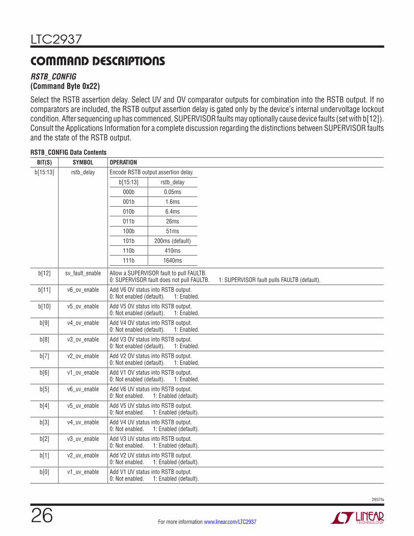
COMMAND DESCRIPTIONSRSTB_CONFIG(Command Byte 0x22)
Select the RSTB assertion delay. Select UV and OV comparator outputs for combination into the RSTB output. If no comparators are included, the RSTB output assertion delay is gated only by the device’s internal undervoltage lockout condition. After sequencing up has commenced, SUPERVISOR faults may optionally cause device faults (set with b[12]). Consult the Applications Information for a complete discussion regarding the distinctions between SUPERVISOR faults and the state of the RSTB output.
RSTB_CONFIG Data ContentsBIT(S) SYMBOL OPERATION
b[15:13] rstb_delay Encode RSTB output assertion delay.
b[15:13] rstb_delay
000b 0.05ms
001b 1.6ms
010b 6.4ms
011b 26ms
100b 51ms
101b 200ms (default)
110b 410ms
111b 1640ms
b[12] sv_fault_enable Allow a SUPERVISOR fault to pull FAULTB. 0: SUPERVISOR fault does not pull FAULTB. 1: SUPERVISOR fault pulls FAULTB (default).
b[11] v6_ov_enable Add V6 OV status into RSTB output. 0: Not enabled (default). 1: Enabled.
b[10] v5_ov_enable Add V5 OV status into RSTB output. 0: Not enabled (default). 1: Enabled.
b[9] v4_ov_enable Add V4 OV status into RSTB output. 0: Not enabled (default). 1: Enabled.
b[8] v3_ov_enable Add V3 OV status into RSTB output. 0: Not enabled (default). 1: Enabled.
b[7] v2_ov_enable Add V2 OV status into RSTB output. 0: Not enabled (default). 1: Enabled.
b[6] v1_ov_enable Add V1 OV status into RSTB output. 0: Not enabled (default). 1: Enabled.
b[5] v6_uv_enable Add V6 UV status into RSTB output. 0: Not enabled. 1: Enabled (default).
b[4] v5_uv_enable Add V5 UV status into RSTB output. 0: Not enabled. 1: Enabled (default).
b[3] v4_uv_enable Add V4 UV status into RSTB output. 0: Not enabled. 1: Enabled (default).
b[2] v3_uv_enable Add V3 UV status into RSTB output. 0: Not enabled. 1: Enabled (default).
b[1] v2_uv_enable Add V2 UV status into RSTB output. 0: Not enabled. 1: Enabled (default).
b[0] v1_uv_enable Add V1 UV status into RSTB output. 0: Not enabled. 1: Enabled (default).

LTC2937
272937fa
For more information www.linear.com/LTC2937
COMMAND DESCRIPTIONSFAULT_RESPONSE(Command Byte 0x23)
The FAULT_RESPONSE command defines the LTC2937 response to system faults (SEQUENCE, SUPERVISOR, CON-TROL or OTHER). An OTHER fault may occur from external pull-down on the FAULTB output, or a loss of SHARE_CLK operation (mask EXTERNAL faults with b[9]). FAULTB pulls low after any of these faults occur.
A freeze mode is available, stopping the sequencing process (if any) and leaving any enabled supplies turned on. This mode should be used with care and is discussed in the applications information.
Automatic re-sequencing is permitted on a time basis or voltage basis, depending on the fault_response_action bits b[4:3]. Using voltage basis, automatic re-sequencing is allowed when monitored supplies have decayed below their respective discharge thresholds. Using time basis allows re-sequencing after 1 of 8 selectable time delays with b[7:5] (without regard to the level of the monitored input voltages). Retries using the combined basis of discharge condition and time delay is also available. Another option is to continue without shutdown, as if nothing is wrong (FAULTB still pulls low).
Set the number of retries allowed with b[2:0]. Retrieve the number of retries attempted (with b[13:11]) after the initial sequencing operation.
Consult the Applications Information for a complete discussion regarding the definition of SEQUENCE, SUPERVISOR, CONTROL and OTHER faults, including more information concerning fault response operations.

LTC2937
282937fa
For more information www.linear.com/LTC2937
The FAULT_RESPONSE data content is shown below.
FAULT_RESPONSE Data ContentsBIT(S) SYMBOL OPERATION
b[15:14] reserved Ignore.
b[13:11] retry_count Read the number of retries attempted. The counter is cleared with any new sequencing-up operation initiated by the ON input or I2C command. The counter may also be cleared using the CLEAR command (read only).
b[10] faultb_state Read the state of FAULTB (read only).
b[9] faultb_mask Select device response to external pull-down on FAULTB. 0: Ignore external FAULTB pull-down (default). 1: Respond to external FAULTB pull-down. Sequenced ENn outputs pull down immediately if not frozen with b[8] below.
b[8] freeze Select system freeze response due to a fault. 0: Do not freeze on fault (default). 1: Freeze device state on fault.
b[7:5] retry_delay Specify the delay between automatic re-sequencing retries.
b[7:5] retry_delay
000b 0.05 ms (default)
001b 200ms
010b 410ms
011b 820ms
100b 1.64s
101b 3.28s
110b 6.55s
111b 13.1s
b[4:3] fault_response_action
Select shutdown and restart action after a fault. Consult applications information for more details.
b[4:3] fault_response_action
00b Continue operation
01b Discharged retry (default)
10b Delayed retry
11b Discharge and Delay retry
b[2:0] retry_number Specify the automatic retry count. Consult applications information for more details.
b[2:0] retry_number
000b 0 (default)
001b 1
010b 2
011b 3
100b 4
101b 5
110b 6
111b Unlimited retries
COMMAND DESCRIPTIONS

LTC2937
292937fa
For more information www.linear.com/LTC2937
COMMAND DESCRIPTIONSMONITOR_STATUS_HISTORY(Command Byte 0x26)
The MONITOR_STATUS_HISTORY command returns two bytes of information with a summary of present and past SUPERVISOR and SEQUENCE faults. Consult the Applications Information section for a complete definition of SU-PERVISOR and SEQUENCE faults. Detected SEQUENCE faults are reported with the lowest numbered channel having report priority. SUPERVISOR faults can only occur through comparators mapped to the reset logic. A valid sequence-up initiation automatically clears the MONITOR_STATUS_HISTORY. Use the CLEAR command (0x2E) to reset the history contents to 0x0000.
MONITOR_STATUS_HISTORY Data Contents (read only)BIT(S) SYMBOL OPERATION
b[15:13] sf_chan_hist SEQUENCE fault channel. Lowest numbered channel has report priority.
b[15:13] sf_channel
000b No fault
001b V1
010b V2
011b V3
100b V4
101b V5
110b V6
111b reserved
b[12] sv_fault_status SUPERVISOR fault status. 0: SUPERVISOR fault has not occurred. 1: SUPERVISOR fault has occurred.
b[11] v6_ov_sv_fault V6 OV SUPERVISOR fault history. 0: No fault. 1: Fault occurred.
b[10] v6_uv_sv_fault V6 UV SUPERVISOR fault history. 0: No fault. 1: Fault occurred.
b[9] v5_ov_sv_fault V5 OV SUPERVISOR fault history. 0: No fault. 1: Fault occurred.
b[8] v5_uv_sv_fault V5 UV SUPERVISOR fault history. 0: No fault. 1: Fault occurred.
b[7] v4_ov_sv_fault V4 OV SUPERVISOR fault history. 0: No fault. 1: Fault occurred.
b[6] v4_uv_sv_fault V4 UV SUPERVISOR fault history. 0: No fault. 1: Fault occurred.
b[5] v3_ov_sv_fault V3 OV SUPERVISOR fault history. 0: No fault. 1: Fault occurred.
b[4] v3_uv_sv_fault V3 UV SUPERVISOR fault history. 0: No fault. 1: Fault occurred.
b[3] v2_ov_sv_fault V2 OV SUPERVISOR fault history. 0: No fault. 1: Fault occurred.
b[2] v2_uv_sv_fault V2 UV SUPERVISOR fault history. 0: No fault. 1: Fault occurred.
b[1] v1_ov_sv_fault V1 OV SUPERVISOR fault history. 0: No fault. 1: Fault occurred.
b[0] v1_uv_sv_fault V1 UV SUPERVISOR fault history. 0: No fault. 1: Fault occurred.

LTC2937
302937fa
For more information www.linear.com/LTC2937
CLEAR_ALERTB(Command Byte 0x28)
Release the ALERTB output pull-down by performing a read from the CLEAR_ALERTB register. All other status information remains unaffected. The returned data word contains no useful information and the contents should be ignored.
STORE(Command Byte 0x2C)
Send the STORE command whenever the current operating configuration requires saving to nonvolatile memory. Future power-on events automatically load the stored operating configuration. The STORE command is ignored when the WP input is high and/or b[0] of the WRITE_PROTECTION register is equal to 1. Write permission is guarded by a 14-bit security key providing additional security to stored content. The STORE command is best used while controlled supplies are off or sequenced-down, to prevent unintended results.
RESTORE(Command Byte 0x2D)
Send the RESTORE command whenever the current operating configuration requires an update from nonvolatile memory. A restore from EEPROM occurs automatically when emerging from power-on reset after device power is applied. The RESTORE command is best used while controlled supplies are off or sequenced-down, to prevent unintended results.
CLEAR(Command Byte 0x2E)
Send the CLEAR command to clear active status, fault and volatile history information. The CLEAR command also resets the sequencing state machine so it is best used while controlled supplies are off or sequenced-down to pre-vent inadvertent system operation. Affected registers are: STATUS_INFORMATION, MONITOR_STATUS_HISTORY, MONITOR_STATUS and SEQ_POSITION_COUNT, ON_OFF_CONTROL b[7] and FAULT_RESPONSE b[13:11]. If CLEAR is immediately followed by a STORE command, the MONITOR_BACKUP register is also cleared.
COMMAND DESCRIPTIONS

LTC2937
312937fa
For more information www.linear.com/LTC2937
COMMAND DESCRIPTIONSSTATUS_INFORMATION(Command Byte 0x29)
The STATUS_INFORMATION command returns a summary of faults and sequencing status flags which have occurred. The register is self-clearing at the beginning of a new sequence-up operation or after a power-on reset. One exception is mb_state (b[12]) which indicates whether or not the MONITOR_BACKUP register has been written. After a power-on reset, b[12] is updated automatically. Perform a CLEAR command followed by a STORE command to reset b[12] to logic low.
STATUS_INFORMATION Data Contents (read only)BIT(S) SYMBOL OPERATION
b[15:13] sf_channel SEQUENCE fault channel. Lowest numbered channel has report priority.
b[15:13] sf_channel
000b No fault
001b V1
010b V2
011b V3
100b V4
101b V5
110b V6
111b reserved
b[12] mb_state MONITOR_BACKUP register status. 0: MONITOR_BACKUP empty. 1: MONITOR_BACKUP written.
b[11:10] local_seq_status Addressed device sequencing status. 00b: Sequence-down complete (power-on default state). 01b: Sequence-up in progress. 11b: Sequence-up complete. 10b: Sequence-down in progress.
b[9:8] group_seq_status Device group sequencing status (for multiple devices connected to SPCLK). 00b: Sequence-down complete (power-on default state). 01b: Sequence-up in progress. 11b: Sequence-up complete. 10b: Sequence-down in progress.
b[7] seq_up_fault Maximum rise time fault. 0: No fault. 1: Fault occurred.
b[6] seq_down_fault Maximum fall time fault. 0: No fault. 1: Fault occurred.
b[5] ov_fault SUPERVISOR fault caused by mapped OV condition. 0: No fault. 1: Fault occurred.
b[4] uv_fault SUPERVISOR fault caused by mapped UV condition. 0: No fault. 1: Fault occurred.
b[3] sv_fault SUPERVISOR fault status. 0: No fault. 1: Fault occurred.
b[2] discharge Discharge status. 0: One or more sequenced voltages are above discharge thresholds. 1: All sequenced voltages are below discharge thresholds.
b[1] seq_control_fault Sequence CONTROL fault status. 0: No fault. 1: Fault.
b[0] other_fault EXTERNAL fault or SHARE_CLK fault status. 0: No fault. 1: Fault occurred.

LTC2937
322937fa
For more information www.linear.com/LTC2937
COMMAND DESCRIPTIONSBREAK_POINT(Command Byte 0x2A)
Pause sequencing at any valid sequence position (occurs during SPCLK low period). Set sequence position break points in the sequence-up or sequence-down phase of operation. Enable break point usage with bp_enable b[10]. With break point usage enabled, a valid control input (ON transition or I2C command) will sequence the device until sp_count in the SEQ_POSITION_COUNT register is equal to bp_value in the BREAK_POINT register. Perform register inspections and system measurements at each paused sequence position. Increment the BREAK_POINT register repeatedly for controlled single stepping through all sequence positions. SPCLK holds low until bp_value is changed to be not equal to sp_count or bp_enable is set low. The sequencing enable delay timers and maximum rise/fall timers function normally at each sequence position.
BREAK_POINT Data ContentsBIT(S) SYMBOL OPERATION
b[15:11] reserved Ignore.
b[10] bp_enable Break point mode. 0: Break point mode not enabled (default). 1: Break point mode enabled.
b[9:0] bp_value Break point sequence position value. Specify a sequence position break point from 0 to 1023. (Default = 0x000).
SEQ_POSITION_COUNT(Command Byte 0x2B)
Read the current sequence position count contained in the sp_count bit field. The sp_count bit field is zero after initial application of device power or after a CLEAR command. At the conclusion of all sequence-up or sequence-down opera-tions, sp_count increments by one. For example, if the last configured sequence position is 10, sp_count increments to 11 when the sequencing operation completes. If the last sequence position is 1023, sp_count rolls over to zero at the end of sequencing. After a fault (whether in break point mode or normal operation), the current sequence position value is reported until the fault exit conditions are satisfied.
SEQ_POSITON_COUNT Data Contents (read only)BIT(S) SYMBOL OPERATION
b[15:11] reserved Ignore.
b[10] sp_bp_test Compare sp_count with bp_value. 0: sp_count is not equal to bp_value. 1: sp_count is equal to bp_value.
b[9:0] sp_count Sequence position count.
LTC2937
332937fa
For more information www.linear.com/LTC2937
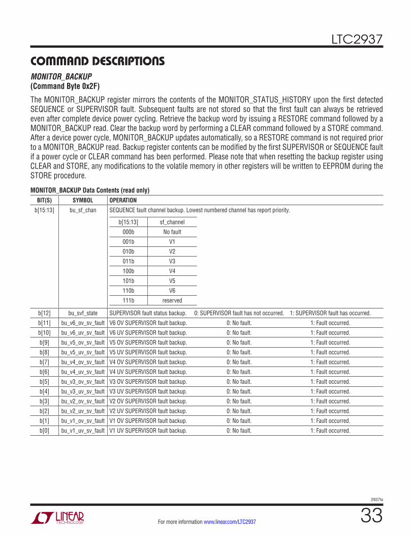
COMMAND DESCRIPTIONSMONITOR_BACKUP(Command Byte 0x2F)
The MONITOR_BACKUP register mirrors the contents of the MONITOR_STATUS_HISTORY upon the first detected SEQUENCE or SUPERVISOR fault. Subsequent faults are not stored so that the first fault can always be retrieved even after complete device power cycling. Retrieve the backup word by issuing a RESTORE command followed by a MONITOR_BACKUP read. Clear the backup word by performing a CLEAR command followed by a STORE command. After a device power cycle, MONITOR_BACKUP updates automatically, so a RESTORE command is not required prior to a MONITOR_BACKUP read. Backup register contents can be modified by the first SUPERVISOR or SEQUENCE fault if a power cycle or CLEAR command has been performed. Please note that when resetting the backup register using CLEAR and STORE, any modifications to the volatile memory in other registers will be written to EEPROM during the STORE procedure.
MONITOR_BACKUP Data Contents (read only)BIT(S) SYMBOL OPERATION
b[15:13] bu_sf_chan SEQUENCE fault channel backup. Lowest numbered channel has report priority.
b[15:13] sf_channel
000b No fault
001b V1
010b V2
011b V3
100b V4
101b V5
110b V6
111b reserved
b[12] bu_svf_state SUPERVISOR fault status backup. 0: SUPERVISOR fault has not occurred. 1: SUPERVISOR fault has occurred.
b[11] bu_v6_ov_sv_fault V6 OV SUPERVISOR fault backup. 0: No fault. 1: Fault occurred.
b[10] bu_v6_uv_sv_fault V6 UV SUPERVISOR fault backup. 0: No fault. 1: Fault occurred.
b[9] bu_v5_ov_sv_fault V5 OV SUPERVISOR fault backup. 0: No fault. 1: Fault occurred.
b[8] bu_v5_uv_sv_fault V5 UV SUPERVISOR fault backup. 0: No fault. 1: Fault occurred.
b[7] bu_v4_ov_sv_fault V4 OV SUPERVISOR fault backup. 0: No fault. 1: Fault occurred.
b[6] bu_v4_uv_sv_fault V4 UV SUPERVISOR fault backup. 0: No fault. 1: Fault occurred.
b[5] bu_v3_ov_sv_fault V3 OV SUPERVISOR fault backup. 0: No fault. 1: Fault occurred.
b[4] bu_v3_uv_sv_fault V3 UV SUPERVISOR fault backup. 0: No fault. 1: Fault occurred.
b[3] bu_v2_ov_sv_fault V2 OV SUPERVISOR fault backup. 0: No fault. 1: Fault occurred.
b[2] bu_v2_uv_sv_fault V2 UV SUPERVISOR fault backup. 0: No fault. 1: Fault occurred.
b[1] bu_v1_ov_sv_fault V1 OV SUPERVISOR fault backup. 0: No fault. 1: Fault occurred.
b[0] bu_v1_uv_sv_fault V1 UV SUPERVISOR fault backup. 0: No fault. 1: Fault occurred.

LTC2937
342937fa
For more information www.linear.com/LTC2937
COMMAND DESCRIPTIONSMONITOR_STATUS(Command Byte 0x30)
The MONITOR_STATUS command returns a summary of the present (live) voltage monitor conditions. UV and OV status are always active. The external status of the RSTB I/O is reported on b[12] and will indicate low if an external device is pulling down on RSTB. Comparator live status is not affected by settings in the RSTB_CONFIG register.
MONITOR_STATUS Data Contents (read only)BIT(S) SYMBOL OPERATION
b[15:14] reserved Ignore.
b[13] margin_status Logical representation of the external margin input and/or I2C margin control bit. 0: Margin function inactive. 1: Margin function active.
b[12] rstb_status Status of the RSTB I/O. 0: RSTB is high. 1: RSTB is low.
b[11] v6_ov_status V6 OV comparator live status. 0: No violation. 1: High limit violation.
b[10] v6_uv_status V6 UV comparator live status. 0: No violation. 1: Low limit violation.
b[9] v5_ov_status V5 OV comparator live status. 0: No violation. 1: High limit violation.
b[8] v5_uv_status V5 UV comparator live status. 0: No violation. 1: Low limit violation.
b[7] v4_ov_status V4 OV comparator live status. 0: No violation. 1: High limit violation.
b[6] v4_uv_status V4 UV comparator live status. 0: No violation. 1: Low limit violation.
b[5] v3_ov_status V3 OV comparator live status. 0: No violation. 1: High limit violation.
b[4] v3_uv_status V3 UV comparator live status. 0: No violation. 1: Low limit violation.
b[3] v2_ov_status V2 OV comparator live status. 0: No violation. 1: High limit violation.
b[2] v2_uv_status V2 UV comparator live status. 0: No violation. 1: Low limit violation.
b[1] v1_ov_status V1 OV comparator live status. 0: No violation. 1: High limit violation.
b[0] v1_uv_status V1 UV comparator live status. 0: No violation. 1: Low limit violation.
DEVICE_ID(Command Byte 0x31)
The DEVICE_ID command returns two bytes containing the part number 0x2937. This register is read only.

LTC2937
352937fa
For more information www.linear.com/LTC2937
APPLICATIONS INFORMATIONIntroduction
The LTC2937 power management IC provides time and event based sequencing, undervoltage and overvoltage supervision and fault management.
Powering the LTC2937
Two options exist for applying LTC2937 device power. If an intermediate bus voltage between 4.5V and 16.5V is available, connect it to the VPWR input. An internal linear regulator converts VPWR down to 3.3V which drives all internal circuitry. The regulated 3.3V also drives VDD and requires a 2.2µF (or greater) compensation capacitor. Alternatively, apply an external supply voltage between 2.9V and 5.5V directly to VDD and VPWR. When driving VDD directly, a compensation capacitor is not required, but a decoupling capacitor (0.1µF) is recommended.
Figure 6. Powering LTC2937 Directly from an Intermediate Bus Voltage
Figure 7. Powering LTC2937 Directly from Low Supply Voltage
Write Protection
To prevent accidental writes to memory (volatile and nonvolatile), apply the software and/or hardware lock functions. Software protection is active when the WRITE_PROTECTION register lock bit b[0] = 1. Deactivate the software lock by writing bit[0] = 0 while matching the 14 bit key string contained in b[15:2]. The hardware lock is active when the WP input is pulled to VDD. Deactivate the hardware lock by pulling the WP input to ground.
Write protection must be de-activated when it is desired to write changes to the volatile or nonvolatile memory. The usual cause of seemingly ignored write operations is due to active write protection. The LTC2937 will acknowledge I2C commands while under write protection. However, the part configuration will not change.
Updating Volatile or Nonvolatile Memory
Changes to the EEPROM require a 2-step procedure. First, write desired values to the command registers. Then, perform the STORE command. Command register configuration will be copied to the EEPROM. Maximum write time is 120ms. Perform a RESTORE command to move EEPROM data into the volatile command registers. The LTC2937 does not acknowledge commands while the EEPROM is writing.
Volatile command register contents are often changed during system testing or development. If desired, restore the command register contents to the stored configuration in EEPROM by performing the RESTORE command. To prevent unintended operation, send the RESTORE command after sequence-down and after sending a CLEAR command. A RESTORE is performed automatically at initial device power-on.
Changes to the volatile memory can be performed at any time. However, some changes should only be made when the system is in the sequenced-down or off state because writes to volatile memory have immediate influence. If the system is actively sequencing or monitoring, and certain changes occur, unintended consequences may
During initial application of LTC2937 device power, device configuration transfers from EEPROM into the volatile operating memory after VDD exceeds undervoltage lockout. The restore time is 2ms maximum. Perform changes to device configuration, sequencing and/or supervisory operations after completion of the restore procedure.
C12.2µF
LTC2937
VPWR
VDDGND
4.5V ≤ VPWR ≤ 16.5VC2
0.1µF
2937 F06
LTC2937
VPWR
VDDGND
2.9V ≤ VDD ≤ 5.5V
2937 F07
C10.1µF

LTC2937
362937fa
For more information www.linear.com/LTC2937
APPLICATIONS INFORMATIONresult because of contradictions within the sequencing state machine. To prevent unintended operation, send a CLEAR command after sequence-down, prior to making changes to volatile memory. Use caution when writing the following commands during the sequencing and monitor-ing phases of operation:
• ON_OFF_CONTROL b[5, 1, 0]
• V_RANGE
• V_THRESHOLD_n
• TON_TIMERS_n
• TOFF_TIMERS_n
• SEQ_UP_POSITION_n
• SEQ_DOWN_POSITION_n
• RSTB_CONFIG
• FAULT_RESPONSE
• CLEAR, STORE, RESTORE
Certain registers have reserved bits in some bit locations. To avoid confusion, mask out or ignore those bits when reading back the contents of those registers. Each command description details the location of the reserved bits. When writing to commands with reserved bits, data content in those bit locations are disregarded.
Figure 8. SPCLK Nominal Timing
Figure 9. SPCLK Stretching
Sequence Position Clock (SPCLK)
When a system requires more than six controlled power supplies, use SPCLK to maintain seamless multi-channel sequencing control across all devices. SPCLK is a single wire event control signal and other than the simple interconnection of SPCLK between devices, additional external device connections to SPCLK are not required or recommended.
Using SPCLK, up to 300 power supplies can be controlled by connecting up to 50 LTC2937s together. Arrange power supply sequence order in any one of 1023 available sequence positions. When applying device power directly to VDD, connect VDD together across all devices. When applying device power to VPWR, the regulated VDD outputs do not require parallel connection.
After initial device power is applied, SPCLK holds low in the non-sequencing phase of operation. Once sequencing is initiated, SPCLK pulls high for 60µs (tHI) and then pulls low. The system is now in sequence position 1. If there are no supplies scheduled for sequencing in position 1, SPCLK pulls high again after 20µs (tLO). SPCLK remains high for 60µs (tHI) and then pulls low again. This cycle repeats (Figure 8) until a power supply scheduled for sequencing is encountered.
ON
SPCLK 1 2 3
SEQUENCEPOSITION NUMBER
2937 F08(tLO)(tHI)
tONSQ
2937 F09
(tHI)
ON
SPCLK 1 2
(UNASSIGNED)
(UV THRESHOLD)
SUPPLY ASUPPLY B
Vn
SPCLK STRETCHING

LTC2937
372937fa
For more information www.linear.com/LTC2937
APPLICATIONS INFORMATIONDuring the sequence-up phase, enable outputs on any LTC2937 scheduled for a particular sequence position pull high after their respective turn-on delay. Turn-on delay is measured from the falling edge of SPCLK. The delay times are individually programmed for each enable output. SPCLK is stretched and remains low (Figure 9) until all supplies scheduled for the current sequence position have crossed their UV threshold. SPCLK then pulls high for 60µs (tHI) and again pulls low, placing all devices into the next sequence position. The process repeats until all power supplies scheduled for sequencing have completed powering up. After the last power supply powers up, SPCLK pulls high for 320µs (tFLOAT) and then pulls low. The sequence-up phase of operation is complete. SPCLK operates in the same manner during sequence-down operation.
Enable any number of supplies in any sequence position using any number of LTC2937s (Figure 9). When using multiple LTC2937s, freely interleave power supply sequencing between devices. For example, enable any number of supplies on a first device, then enable any number of supplies on another device, then again from the first device and so forth. Reserve certain sequence positions for possible insertion of additional power supplies. Note that in Figure 9, sequence position 1 is unassigned or reserved for future use. Leaving sequence positions unassigned can be good practice during system development as it allows for future expansion or insertion of supplies without having to reprogram all LTC2937's in the system. Simply position a new supply in an unassigned sequence position and all succeeding positions slide appropriately.
System Configuration
The procedure described herein is intended as a reference and for the purpose of understanding the registers in a software development environment. Configure LTC2937 standalone operation using the LTC USB to I2C/SMBus/PMBus controller (DC1613) and LTpowerPlay software GUI using intuitive menu driven objects.
Simplify the procedure of system configuration by configuring command register contents in a task oriented manner. For example, a typical system can be divided into four regions of operation:
1. Sequence-Up and Sequence-Down Control
(select sequence initiation method)
2. Sequence-Up Parameters
(sequence-up order, time spacing and maximum rise time)
3. Voltage Supervision
(monitored voltage range, voltage threshold and reset response)
4. Sequence-Down Parameters
(sequence-down order, time spacing and maximum fall time)
Beyond the sequence and supervisory commands are a set of commands for fault management, status information, system debug and general information. These commands are discussed further below. Note that the command summary table is also organized in a task oriented fashion.
Sequence-Up and Sequence-Down Control
Various sequence-up and sequence-down control options are specified through the ON_OFF_CONTROL command. To initiate sequencing, use the polarity selectable ON input and/or I2C on/off bit. If specifications require sequencing-up to begin with discharged supplies, set b[5]=1 to enforce qualification.
If b[5] = 1, the LTC2937 prohibits initial sequencing until supplies configured for sequencing are discharged. If a fault has occurred and automatic retries are enabled, re-sequencing conditions obey the discharge and/or time delay rules specified in the FAULT_RESPONSE register.
To start sequence-down operations, switch the ON input or I2C on/off bit to the off state. Sequence positions are advanced on the basis of sequenced supply voltage level or configured time-delay. Select this distinction with ON_OFF_CONTROL b[0].
The i2c_on_off_mask and on_input_mask bits (b[3:2]) are set low by default. This prevents any sequencing from occurring at initial application of device power. Since the ON input has an internal pull-up current source, automatic sequencing is possible (with default ON polarity) if the on_input_mask = 1 and the ON input is not held low.

LTC2937
382937fa
For more information www.linear.com/LTC2937
APPLICATIONS INFORMATION
Figure 10. Sequence-Up Timing Parameters (V1 Set to Sequence Up in Sequence Position 2) Showing SEQUENCE Fault
Sequence-Up Parameters
Sequence-up configuration consists of defining the sequence position for each sequenced supply, the time delay to enable (measured from the falling edge of SPCLK) and the maximum allowed elapsed time (from enable) for each sequenced supply to reach its UV threshold. Con-figure these parameters with the SEQ_UP_POSITION_n and TON_TIMERS_n commands (where n denotes the channel number).
Figure 10 graphically depicts parameters for a hypotheti-cal supply operating in channel 1. Sequencing is initiated with the ON input. In this example, the supply is enabled in sequence position 2, with an enable delay (ton_delay_1) of 800µs and a maximum rise time (ton_max_1) of 10.24ms. Because V1 does not meet its rise time requirements (V1 is below uv_threshold_1 when ton_max is reached), a sequence-up fault occurs and all enables are turned off. The corresponding command register values are:
SEQ_UP_POSITION_1 = 0x0002
TON_TIMERS_1 = 0x8064
Voltage Supervision
There are three steps to programming voltage supervision. First, configure the voltage range for each monitored input. Second, configure the UV, OV and discharge thresholds for each monitored input. Lastly, decide on which monitored inputs contribute to the RSTB response.
The LTC2937 provides 12 independently programmable high accuracy voltage monitor comparators. There are two comparators per Vn input, typically used for un-dervoltage and overvoltage detection. Each comparator provides 750 thresholds (250 thresholds in each of 3 voltage input ranges), from 0.2V to 6V. Additionally, each Vn input contains a discharge comparator which determines when monitored voltages have decayed to a substantially low level.
Voltage Monitor Range
The V_RANGE command contains encoding to program the voltage threshold range for each of the six monitor inputs (V1 through V6). The range selection applies to the OV and UV comparators connected to each input. The High Range covers thresholds between 1V and 6V in 20mV steps. The Low Range covers thresholds between 0.5V and 3V in 10mV steps. The Adjustable Range covers 0.2V to 1.2V in 4mV steps. Select the negative polarity option in the Adjustable Range when sensing negative voltages. The Adjustable Range is high impedance. If the Adjust-able Range is used in conjunction with external resistive dividers, keep the Thevenin divider resistance below 100k to maintain threshold accuracy.
Because there are 750 fixed thresholds per comparator, external resistive dividers are rarely necessary. This keeps part counts low and board layout simple. When monitored
2937 F10
ON
SPCLK 1 2
EN1
V1
FAULTB
uv_threshold_1
ton_delay_1 ton_max_1

LTC2937
392937fa
For more information www.linear.com/LTC2937
supplies are below 6V, consider using one of the fixed thresholds in any of the three monitoring ranges.
UV and OV Thresholds
Each V_THRESHOLD_n command (n = 1..6) configures the UV and OV thresholds for the corresponding input channel. Each command word contains encoding for the OV threshold in the upper byte, and for the UV threshold in the lower byte. Voltage threshold encoding examples are given below the command description.
In the High Range and Low Range modes, the Vn inputs have finite input impedance, and should not be loaded with an external resistive divider. In the Adjustable Range, the Vn inputs are high impedance. Use the adjustable range with or without external resistors to customize thresholds. At each Vn input, the adjustable range senses voltages between 0.2V and 1.2V. External resistors can divide-down larger voltages, and provide level-shifting for negative voltage applications.
UV Thresholds and Sequence-Up Hysteresis
During sequencing-up, systems are subject to large electrical disturbances as loads become energized. Each of the LTC2937 comparators has built-in glitch filtering, and accommodation for short-term sagging in supervised voltages during sequence-up. The UV thresholds on chan-nels selected for sequencing receive temporary hysteresis during sequencing-up. Each UV threshold moves down by 5% (for positive sensing applications) after the voltage first crosses its configured UV threshold. The temporary hysteresis remains effective for ½ of the configured RSTB assertion delay. The RSTB assertion delay commences when the last configured supply rises above its UV thresh-old for the first time (supplies configured for sequencing and for RSTB logic).
For negative sensing applications, hysteresis moves the UV threshold up by 5%, instead of down. The UV threshold during temporary hysteresis is equal to the programmed threshold. When temporary hysteresis is not active, the UV threshold is 5% below the value configured by the V_THRESHOLD_n word. This is important because the UV threshold used in all negative calculations is 5% below that programmed in the V_THRESHOLD_n word.
APPLICATIONS INFORMATIONIf a channel is not combined into the RSTB response, its UV comparator threshold does not move. For positive sensing applications it remains at the value encoded in the V_THRESHOLD_n word, and for negative sensing applications it remains at a value 5% below the value encoded in the V_THRESHOLD_n word.
Selecting Resistors for Adjustable Range
For positive voltage sensing applications, use Figure 11 as a configuration reference. For example, assume a positive input voltage of +15V applied to the top of R2, with a de-sired UV threshold at 14.3V (VTH(UV)). Use the V_RANGE command to select the Positive Adjustable Range. When the input voltage is 14.3V we choose the Vn input to be VMON(UV) = 1.0V (somewhat arbitrarily, for numerical simplicity). VMON(UV) = 1.0V is a code of uv_threshold_n = 0xCD (205). The resistor ratio, R2/R1 is easily determined by the equation:
R2R1
=VTH(UV) – VMON(UV)( )
VMON(UV)=
(14.3V –1V)1V
= 13.3
Suitable values are R1 = 10k and R2 = 133k. With a Thevenin divider resistance of less than 10k, leakage current in the Vn pin causes less than 0.01% threshold error. Errors in the resistor ratio will produce proportional voltage threshold errors.
Figure 11. Configuring Custom Positive Thresholds (Operating in the Positive Adjustable Range)
2937 F11
LTC2937
Vn
POSITIVEMONITORED
SUPPLY
R2
VMON(OV)
VMON(UV)
VDTH0.12V
R1
–
+
–
+
–
+

LTC2937
402937fa
For more information www.linear.com/LTC2937
Figure 12. Configuring Custom Negative Thresholds (Operating in the Negative Adjustable Range)
2937 F12
LTC2937
Vn
VDD
NEGATIVEMONITORED
SUPPLY
R2
VMON(OV)
0.95 • VMON(UV)
VDTH1.2V
R1
–
+
–
+
–
+
APPLICATIONS INFORMATIONCalculations for negative input voltage applications are more complex due to level shifting and temporary input hysteresis. Use Figure 12 as a configuration reference. Because the voltage at the Vn input must be between 0.2V and 1.2V in the adjustable range (at threshold), a positive level-shifting voltage (VLS) is required. VLS must be stable before the negative voltage pulls down to prevent the Vn input voltage from going below ground. Level-shifting volt-age accuracy affects threshold sensing accuracy. Use VDD as a convenient level-shifting voltage when ±2% threshold variation is tolerable. Use a more accurate level-shifting voltage for better than 2% threshold accuracy.
For any negative sensing application, the actual UV com-parator threshold is 5% below the value programmed in the V_THRESHOLD_n word. For example, if the UV comparator is programmed for the top of the adjustable range (1.2V), the comparator will trip at a voltage of 0.95 • 1.2V = 1.14V. This is true whether the supply is partici-pating in sequencing or not. If the supply is participating in sequencing, the temporary hysteresis threshold moves to the value programmed in the V_THRESHOLD_n word.
Consider an example of a negative supply that is not par-ticipating in sequencing (no temporary hysteresis). Assume a negative input voltage of −0.9V applied to the bottom of R1, and a desired UV threshold voltage of VTH(UV) = −0.864V. Use the V_RANGE command to select the Nega-
tive Adjustable Range. When the input voltage is −0.864V, we choose the Vn input to be VMON(UV) = 1.2V. VMON(UV) = 1.2V is a code of uv_threshold_n = 0xFF (255). The resistor ratio, R2/R1 is easily determined by the equation:
R2R1
=VLS – 0.95• VMON(UV)
0.95• VMON(UV) – VTH(UV)=
3.3V –1.14V1.14V +0.864V
≈1.078
Suitable choices for R2 = 22.1k and R1 = 20.5k.
As a final example, consider the case of the negative sup-ply participating in sequencing. Keep the UV threshold VTH(UV) = −0.864V, and select 5% temporary hysteresis (H = 0.05). Select the monitor threshold VMON(UV) = 0.748V (uv_threshold_n = 0x8E (142)). R2/R1 is given by:
R2R1
=VLS – VMON(UV)
VMON(UV) – VTH(UV) •(1–H)
R2R1
=3.3V −0.748V
0.748V +0.864V •0.95≈1.626
Suitable resistor values are R2 = 17.4k and R1 = 10.7k.
OV Thresholds in Adjustable Applications
After selecting external resistors, configure the OV thresholds. Following the positive adjustable example of Figure 11, the monitor comparator OV threshold is determined from:
VMON(OV) =VTH(OV)
1+R2R1
Choosing a 10% overvoltage threshold, VTH(OV) = (15V∙1.1) = 16.5V. The monitor threshold becomes:
VMON(OV) =16.5V
1+133k10k
≈1.154V
The closest comparator code (ov_threshold_n) is 0xE3 (243).

LTC2937
412937fa
For more information www.linear.com/LTC2937
APPLICATIONS INFORMATIONFollowing the negative adjustable example of Figure 12, the monitor comparator OV threshold is determined from:
VMON(OV) =VLS +
R2R1
• VTH(OV)
1+R2R1
Choosing a 10% overvoltage threshold:
VTH(OV) = (−0.9V • 1.1) = −0.99V
The monitor threshold becomes:
VMON(OV) =3.3V +
17.4k10.7k
•(−0.99V)
1+17.4k10.7k
≈ 0.644V
The closest comparator code (ov_threshold_n) is 0x74 (116).
RSTB Response
Tie RSTB to any device requiring a reset signal. RSTB is low when any selected voltage monitor violates its respective threshold. RSTB is allowed to pull high when all selected voltages are in compliance (UV and/or OV) and the asser-tion delay has expired. An external pull-up resistor (10k to 100k) is recommended. Use the RSTB_CONFIG com-mand to configure RSTB response. Combine any voltage monitor input into the RSTB response whether or not
the channel is participating in sequencing. If there are no channels selected, RSTB is affected only by the device’s internal undervoltage lockout and initialization circuits. The assertion delay remains active. After initial application of device power, RSTB assertion delay cannot start until device configuration is complete. The configuration (or restore) time (tRT) is a maximum of 2ms after crossing VDD undervoltage lockout (VUVL).
Force RSTB high anytime by pulling the MARGB input low. MARGB overrides the RSTB function and is typically used while system voltages are margined high or low and a device reset is not desired. The RSTB override may also be controlled with I2C writes to b[6] of the ON_OFF_CONTROL register.
Sequence-Down Parameters
Sequence-down configuration consists of defining the sequence position for each sequenced supply, the time delay to enable pulling low (measured from the falling edge of SPCLK) and the maximum allowed elapsed time (from enable) for each sequenced supply to reach its discharge threshold. Configure these parameters with the SEQ_DOWN_POSITION_n and TOFF_TIMERS_n com-mands (where n denotes the channel number). Figure 13 graphically depicts parameters for a hypothetical supply operating in channel 1. Sequencing is initiated with the ON input. In this example, the supply is disabled in sequence position 2, with an enable delay (toff_delay_1) of 800µs
Figure 13. Sequence-Down Timing Parameters (V1 Set to Sequence Down in Sequence Position 2)
2937 F13
toff_delay_1 toff_max_1
ON
SPCLK 1 2
EN1
V1
FAULTB
discharge_threshold = V1DTH

LTC2937
422937fa
For more information www.linear.com/LTC2937
APPLICATIONS INFORMATIONand a maximum fall time (toff_max_1) of 10.24ms. Be-cause V1 does not meet its fall time requirements (V1 is above the discharge threshold when toff_max is reached), a sequence-down fault occurs and all enables are turned off. The corresponding command register values are:
SEQ_DOWN_POSITION_1 = 0x0002
TOFF_TIMERS_1 = 0x4064
Two options exist for triggering sequence position ad-vancement during the sequence-down phase of operation. ON_OFF_CONTROL register bit b[0] determines the trig-ger method. The first option (b[0] = 0) allows sequence position advancement on the basis of voltage decay, and applies to all sequenced supplies. A supply (or supplies) that has been commanded off in a particular sequence position is required to fall below its discharge threshold before system advancement to the next sequence position (Figure 13). The decay must occur before the toff_max time has transpired. The second option (b[0] = 1) allows sequence position advancement on the basis of time delay. The time delay is equal to the configured toff_max time. If toff_max is set to ∞, operation reverts back to voltage decay mode.
Discharge Thresholds
The LTC2937 monitor inputs have discharge monitor com-parators with thresholds used to determine if a monitored supply is substantially discharged when in the off state. This feature is used in two ways. First, prevent the start of sequencing-up if any supply scheduled for sequencing is above its discharge threshold. Enable this qualification with b[5] in the ON_OFF_CONTROL register. Second, as discussed above, use b[0] to allow sequence-down advancement when the disabled supplies have decayed below their discharge threshold. Read the combined dis-charge status for sequenced channels from b[2] in the STATUS_INFORMATION register.
The selected voltage range for each monitor input determines the respective discharge threshold value at the monitor input. Operating in the high or low range sets the discharge threshold VDTH to 400mV. Operating in the positive adjustable range sets the discharge threshold VDTH
to 120mV. In the negative adjustable range, the discharge threshold VDTH is 1.2V.
The adjustable ranges are often used in conjunction with external resistive dividers to configure custom thresholds as described earlier. For positive adjustable applications, the discharge threshold (DT) referred to the input voltage is
DT = VTH(UV) •
VDTHVMON(UV)
Applying values from the example using Figure 11, the discharge threshold is:
DT = 14.3V •
0.12V1V
= 1.716V
For negative adjustable applications, the discharge threshold (DT) referred to the negative input voltage is
DT = VDTH −VLS − VDTH( )
R2R1
Applying values from the example using Figure 12, the discharge threshold is:
DT = 1.2V −3.3V −1.2V( )
17.4k10.7k
= −0.091V
Active Supply Discharge
When power supplies are commanded off, system load characteristics and bulk capacitance can make it difficult to discharge supply voltages to a low level quickly. Use the active supply discharge feature to reduce discharge time. Apply b[10] of the respective SEQ_DOWN_POSITION_n register to enable the 30mA pull-down current. The pull-down current is always active while the respective supply is off (enable low). The discharge feature is best used in monitor applications that do not have an external resistive divider at the monitor input. CAUTION: Applying active discharge through a divider network in positive or negative voltage applications can cause a false sense of discharge at the monitor input.

LTC2937
432937fa
For more information www.linear.com/LTC2937
Fault Descriptions
Various faults can be detected during system operation. First fault information is logged to EEPROM. Program fault response actions using the FAULT_RESPONSE command. Actions include total shutdown with optional restart, sys-tem freeze and ignore. Faults can occur due to sequence control violations (CONTROL fault), sequence-up and sequence-down violations, voltage threshold violations, external inputs and loss of SHARE_CLK.
CONTROL Faults
A sequence-up or sequence–down phase is initiated by an ON input change of state and/or i2c_on_off bit state change. After the sequence-up phase has commenced, the ON input and/or i2c_on_off bit must remain in the same state until all sequenced supplies have reached their undervoltage threshold.
Similarly, after the sequence-down phase has commenced, the ON input and/or i2c_on_off bit must remain in the same state until all sequenced supplies have reached their discharge threshold.
A change of sequence control state during sequencing operations is considered a CONTROL fault. A CONTROL fault causes all enable outputs to pull low immediately. The FAULTB output pulls low in response to any CONTROL fault. The reporting of CONTROL fault status is described below in the Fault Reporting section.
To force a shutdown at any time, create an intentional CONTROL fault by toggling the ON input. The width of the ON pulse must be greater than 25µs in order to be detected.
SEQUENCE Faults
Each of the six channels has a dedicated timer defining maximum turn-on and turn-off time for each sequenced voltage, used to protect against stalled power supplies. Any enabled supply that fails to exceed its sequence threshold before its timer expires will cause a SEQUENCE fault. A SEQUENCE fault causes all enable outputs to pull low immediately. The FAULTB output pulls low in response to any SEQUENCE fault. The reporting of SEQUENCE fault status is described below in the Fault Reporting section.
SUPERVISOR Faults
It is important to understand the difference between a SUPERVISOR fault and the RSTB output response. Us-ing the RSTB_CONFIG command (0x22), UV and OV comparator outputs combine to form the RSTB response. The RSTB output is always active (unless masked during margining). SUPERVISOR faults are generated from the same set of selected UV and OV comparators. However, a SUPERVISOR fault is active only under a restricted set of operating conditions.
SUPERVISOR faults are allowed to occur when the sys-tem is in the sequence-up phase or supervisory phase of operation. These phases reside within the time region bracketed by ON input changes of state (rising ON to falling ON under default polarity). Furthermore, UV comparator contributions to a SUPERVISOR fault are only active after the sensed voltages have crossed their UV threshold for the first time. OV comparator contributions are active throughout the sequence-up and supervisory phases of operation. In the event of a SUPERVISOR fault, it may be desirable to turn off all sequenced supplies. Set b[12] = 1 in the RSTB_CONFIG register (0x22), to allow the FAULTB output to pull low in response to a SUPERVISOR fault. All sequenced enable outputs pull low when the fault is generated. The reporting of SUPERVISOR fault status is described below in the Fault Reporting section.
EXTERNAL Faults
It may be desirable to turn off enabled supplies on the basis of an external event. Apply an external signal to pull down on FAULTB and force a shutdown event if b[9] of the FAULT_RESPONSE register is set to a logic 1. To ignore external pull downs on FAULTB, set b[9] to logic 0. The reporting of EXTERNAL fault status is described below in the Fault Reporting section.
SHARE_CLK Faults
If SHARE_CLK becomes inactive for more than 32µs after it has initially started to operate, a fault is automatically generated. The fault causes FAULTB to pull low. All enable outputs pull low when the SHARE_CLK fault is generated. The reporting of SHARE_CLK fault status is described below in the Fault Reporting section.
APPLICATIONS INFORMATION

LTC2937
442937fa
For more information www.linear.com/LTC2937
APPLICATIONS INFORMATIONFault Reporting
Retrieve important fault information from the following useful registers:
• STATUS_INFORMATION (0x29)
• MONITOR_STATUS (0x30)
• MONITOR_STATUS_HISTORY (0x26)
• MONITOR_BACKUP (0x2F)
Obtain device status with an I2C read word operation from STATUS_INFORMATION (command address 0x29). Em-bed the read operation in a software loop for continuous polling. Otherwise, read the register on an as needed basis, for example after ALERTB or FAULTB has pulled low. Fault related data in STATUS_INFORMATION includes:
• SEQUENCE fault channel number
• Monitor backup status
• Sequence-up fault status
• Sequence-down fault status
• OV fault status
• UV fault status
• SUPERVISOR fault status
• CONTROL fault status
• EXTERNAL or SHARE_CLK fault status
Device status at the time of a fault is latched into STATUS_INFORMATION (except for the discharge status in b[2]). This implies that although the system may be commanded off and in the sequence-down state (due to a fault), the STATUS_INFORMATION register will not necessarily indi-cate sequence-down status. The STATUS_INFORMATION register retains the state of the device at the time of the fault until the beginning of the next sequence-up opera-tion, or until cleared.
Other non-fault related data contained in STATUS_INFORMATION includes sequence region status and discharge level status. A valid sequence-up initiation automatically clears STATUS_INFORMATION.
A summary of the present (live) voltage monitor condi-tions and external status of RSTB is available from the MONITOR_STATUS register.
Retrieve a summary of collected SUPERVISOR and SEQUENCE faults with a read from MONITOR_STATUS_HISTORY. If two or more supplies have simultaneous SEQUENCE faults, the sequence fault is reported with the lowest numbered channel having report priority. SUPERVISOR faults can only occur through comparators mapped to the reset logic. A valid sequence-up initiation automatically clears the MONITOR_STATUS_HISTORY. Use the CLEAR command (0x2E) to reset the history contents to the defaults.
The MONITOR_BACKUP register mirrors the contents of the MONITOR_STATUS_HISTORY upon the first detected SEQUENCE or SUPERVISOR fault. Subsequent faults are not stored so that the first fault can always be retrieved even after complete device power cycling. If device power has not been cycled, retrieve the backup word by issuing a RESTORE command followed by a MONITOR_BACKUP read operation. Clear the backup word by performing a CLEAR command followed by a STORE command. After a device power cycle, MONITOR_BACKUP updates automati-cally, so a RESTORE command is not required prior to a MONITOR_BACKUP read. After any device power cycle or CLEAR command, backup register contents are directly modified by the next SUPERVISOR or SEQUENCE fault. Monitoring b[12] of the STATUS_INFORMATION register alerts the existence of a logged fault.
Fault Management
In the event of a fault, a variety of responses can be configured in the FAULT_RESPONSE register (0x23). Response actions include:
• Shut-down and stay off.
• Shut-down and restart after discharging supplies.
• Shut-down and restart after a time delay.
• Shut-down and restart after discharging supplies and time delay.
• Continue operation.
• Freeze system in current state.

LTC2937
452937fa
For more information www.linear.com/LTC2937
APPLICATIONS INFORMATIONSome applications require the ability to retry operation after a shut-down event. Specify the automatic retry count in the FAULT_RESPONSE register (0x23) with b[2:0]. Retry counts can be set to zero, range from one to six, or be unlimited. When configured for retry operation, leave the sequencing control (ON input or I2C directive) in the sequence-up state, unless a sequence-down operation is required. Retries do not occur in response to faults during the sequence-down phase of operation.
The zero retry option is useful when a new system requires some debug or adjustments after initial application of sequenced power. If power supply turn-on does not meet requirements, the fault response action of simply shutting down supplies and remaining off allows for status register inspections without the risk of re-energizing loads improperly. The status information helps determine the source of failure. Re-sequencing is permitted after the ON input has been taken to the sequence-down level and retry conditions specified in b[4:3] have been satisfied.
Some systems can tolerate retry attempts after failed operation. In the one to six retry mode, the retry counter can be read to retrieve the number of attempted retries. With the ON input at the sequence-up level, the retry counter is never cleared automatically. The retry counter is cleared to zero after the ON input has been taken to the sequence-down level and retry conditions have been satisfied.
With unlimited retries selected, retries are attempted continuously, until commanded off (by the ON input, I2C bus or both), device power is removed, or another fault condition causes the device to turn off the power supply enable signals. The retry counter does not count in infinite retry mode.
Certain criteria must be satisfied before a retry occurs. For example, all sequenced supplies may be required to be below their discharge threshold before a retry occurs. This ensures that sequencing begins only after all sequenced supplies have returned to a low voltage level. After a fault, all sequenced enable outputs turn off immediately. FAULTB pulls low if required. Automatic retries are allowed after sequenced voltages have decayed below their discharge thresholds.
Alternatively, allow retries after a specified time delay. Select 1 of 8 time delays between 50µs and 13 seconds. The use of time delay can allow overheated components to drop in temperature before a retry is attempted. After a fault, all sequenced enable outputs turn off immediately. FAULTB pulls low if required. Automatic retries are allowed after the time period specified in b[7:5].
Automatic retries do not occur in the case of CONTROL faults, however CONTROL faults can occur during retry operations. If desired, retries may require both discharge and time delay. The combined discharge and time delay feature is only available when using automatic retries.
The FAULT_RESPONSE register reports the number of retries attempted in b[13:11]. The count is updated when the retry criteria discussed above are met. In a system with multiple LTC2937s, retry counts can differ among devices if some devices have met retry criteria and others have not. If the number of retries allowed is unlimited, the retry counter reports a value of zero.
Avoid changing the allowed number of retries while sequencing control is in the sequence-up state to prevent unintended operation. To safely change configuration, place sequencing control into the sequence-down state, perform a CLEAR operation and then make changes to the retry number.
Systems that experience complete shutdown after a fault can be difficult to debug because the power is gone. The continue and freeze fault response actions can be useful when debugging system problems, because power supplies remain on, allowing for meaningful measurements. However, use caution when applying the continue and freeze modes because some loads are highly sensitive to the applied supply voltages and, if one or more voltages are incorrectly applied, damage to a load may result.
In the continue mode, there is no shutdown except in the case of a CONTROL fault. Information is logged to status registers and a FAULTB output is generated, but shutdown procedures do not take place. EXTERNAL faults are ignored. SPCLK attempts to operate, so a complete sequence-up process can occur even if one or more supplies have a problem. To prepare for restart after a fault in continue mode, bring the ON input to the sequence-down state and perform a CLEAR operation.

LTC2937
462937fa
For more information www.linear.com/LTC2937
APPLICATIONS INFORMATIONIn the freeze mode, fault information is logged to status registers and a FAULTB output is generated, but shutdown procedures do not take place. If the fault occurs during sequencing, SPCLK stops and does not advance further. SHARE_CLK continues to operate normally. ON input state changes are ignored after the original fault. If both freeze mode and continue mode are selected, freeze mode takes precedence. Exit from a freeze condition by setting b[8] = 0 in the FAULT_RESPONSE register (provided that continue mode is not selected) or perform a CLEAR operation. These actions cause enable outputs to pull low, returning the system to a shut-down state.
Fault Debugging Tools
While STATUS_INFORMATION, FAULT_RESPONSE, MONITOR_STATUS_HISTORY, MONITOR_STATUS and MONITOR_BACKUP provide insight into system behavior, additional commands and functions are available to assist with system debug. These include:
• BREAK_POINT (0x2A)
• SEQ_POSITION_COUNT (0x2B)
• SMBus Alert Response Address
The break point feature holds the system at user specified sequence positions during SPCLK low periods. Set sequence position break points in the sequence-up or sequence-down phase of operation. Enable break point usage with bp_enable b[10]. With break point usage enabled, a valid control input (ON transition or I2C command) will sequence the device until sp_count in the SEQ_POSITION_COUNT register is equal to bp_value in the BREAK_POINT register. Perform register inspections and system measurements at each paused sequence position. Increment the BREAK_POINT register repeatedly for controlled single stepping through all sequence positions. SPCLK holds low until bp_value is changed to be not equal to sp_count or bp_enable is set low. The sequencing enable delay timers and maximum rise/fall timers function normally at each sequence position.
Knowing the sequence position after a fault can help identify problems. Read the current sequence posi-tion count contained in the sp_count bit field of the SEQ_POSITION_COUNT register. The sp_count bit field
is zero after initial application of device power or after a CLEAR command. At the conclusion of all sequence-up or sequence-down operations, sp_count increments by one. For example, if the last configured sequence position is 10, sp_count increments to 11 when the sequencing operation completes. If the last sequence position is 1023, sp_count rolls over to zero at the end of sequencing. After a fault (whether in break point mode or normal operation), the current sequence position value is reported until the fault exit conditions are satisfied.
The ALERTB output pulls low in response to any fault. Connect ALERTB as an interrupt to a host processor. The host can access all devices through the Alert Response Address. Only the devices which asserted their ALERTB will acknowledge the Alert Response Address. If more than one device is alerting, the device with the lowest address will return its address as data. After acknowledging the slave address, the slave device releases pull-down on ALERTB. If the host recognizes that ALERTB remains low due to another device, it can read the alert response address again.
The ALERTB output pull-down may also be removed by performing a read from the CLEAR_ALERTB register. All other status information remains unaffected. The returned data word contains no useful information and the contents should be ignored. Faults may persist even though ALERTB is cleared.
Share Clock (SHARE_CLK)
Synchronize multiple LTC2937s (and any other LTC device with a SHARE_CLK function) in an application by connecting together the open-drain SHARE_CLK input/outputs to a pull-up resistor as a wired OR. A single 3.3k resistor is recommended. The fastest clock will take over and synchronize timing on all devices.
Asynchronous Supply Control
Any supply controlled by an LTC2937 enable output may be asynchronously commanded on or off. Activate this capability by setting the respective b[9:0] = 0 in SEQ_UP_POSITION_n or SEQ_DOWN_POSITION_n. To release the enable pull-down and turn on the controlled

LTC2937
472937fa
For more information www.linear.com/LTC2937
APPLICATIONS INFORMATIONsupply, write b[10] = 1 in SEQ_UP_POSITION_n. To shut off the supply, write b[10] = 0.
A supply may be asynchronously turned on before or after sequence-up operations. It is not recommended to turn on supplies asynchronously during sequence-up operations. If a supply has been turned on before sequencing, its re-spective monitor input will be checked for UV compliance in sequence position 1. If the monitor input is not above its configured UV threshold before its respective ton_max time has elapsed (measured from the start of sequence position 1), a SEQUENCE fault is generated.
The UV and OV comparator outputs from asynchronously enabled channels may be combined into the RSTB re-sponse. Furthermore, if the asynchronous channel is en-abled prior to sequencing-up and combined into the RSTB response, it will also contribute to SUPERVISOR faults if the monitored voltage falls back below its UV threshold after sequence-up operations have started.
If an asynchronous channel is enabled after sequencing-up is complete, its UV and OV comparator outputs can still be combined into the RSTB response. However, the comparators will not contribute to SUPERVISOR faults.
After sequence-down operations have completed, a CLEAR command must be issued prior to assigning any asynchro-nously operated channel a position in the sequencing order.
To use the LTC2937 as a simple multi-channel voltage supervisor without sequencing, configure all contributing channels to be asynchronously enabled and configure un-used channels for sequence position zero. Select channels to be combined into the RSTB and optional SUPERVISOR fault responses.
LTpowerPlay: An Interactive GUI for Power System Management
LTpowerPlay is a powerful Windows based development environment that supports Linear Technology power system manager ICs with EEPROM, including the LTC2937 6-channel sequencer and voltage supervisor. The software supports a variety of different tasks. You can use LTpowerPlay to evaluate Linear Technology ICs by connecting to a demo board system. LTpowerPlay can also be used in an offline mode (with no hardware
present) in order to build a multichip configuration file that can be saved and reloaded at a later time. LTpowerPlay provides unprecedented diagnostic and debug features. It becomes a valuable diagnostic tool during board bring-up to program or tweak the power management scheme in a system or to diagnose power issues when bringing up rails. LTpowerPlay utilizes Linear Technology’s DC1613 USB-to-I2C/SMBus/PMBus Controller to communicate with one of many potential targets, including the DC2313 demo board set, the DC2347socketed programming board, or a customer target system. The software also provides an automatic update feature to keep the software current with the latest set of device drivers and documentation. A great deal of context sensitive help is available within LTpowerPlay along with several tutorial demos. Complete information is available at: www.linear.com/ltpowerplay.
External Connection Design Checklist
• Apply device power through VPWR or VDD and ground. If powered through VPWR, place 2.2µF (or greater) compensation capacitor between VDD and GND.
• Tie unused Vn inputs to GND.
• Have control of WP if needed for device programming.
• Have control of ON if needed for sequencing.
• Have control of MARGB if needed for voltage margin-ing operations.
• Use pull-up resistors to ENn as needed (10k to 100k).
• Apply pull-up resistor to SHARE_CLK (3.3k to 10k) and connect to other SHARE_CLK nodes as needed.
• Connect SPCLK to other SPCLK nodes as needed. Do not apply pull-up resistors.
• Use pull-up resistors to RSTB, FAULTB and ALERTB as needed (10k to 100k).
• If using I2C for programming and/or read back:
• Configure device address with ASELn inputs.
• Check addresses for collision with other devices on the I2C bus.
• Verify logic level compatibility for all I/O between LTC2937 and other devices.

LTC2937
482937fa
For more information www.linear.com/LTC2937
APPLICATIONS INFORMATIONMinimum Connections for Programming
For users interested in performing their own programming, Figure 14 shows the minimum recommended connections for a programming socket. Make sure that the SCL and SDA levels match the VDD level. Set the software lock bit to 0 in the WRITE_PROTECTION register before writing new register values. Changing the software lock bit from a 1 to 0 requires matching the key string in b[15:2]. A socketed programming board is available for use with the LTpowerPlay system.
Interconnect Between Multiple LTC2937s
Figure 15 shows how to interconnect the pins in a typical multi-LTC2937 array. In this example, device power is derived from an intermediate bus voltage. It is recom-mended that SPCLK, SHARE_CLK and ON are tied together. Optional interconnections include RSTB, FAULTB, MARGB, ALERTB, SDA and SCL. Connect FAULTB lines together with external fault listening enabled to allow any one fault to shut off all power supplies. The host controller asserts ON for sequencing control and listens to ALERTB to gain information about system faults.
System Event Based Sequencing
The schematic shown on the back page demonstrates how power sequences can be coordinated in a system of systems. A logic output from System 1 (READY) is used as a gating input to the sequence order. System 2 does not sequence-up until System 1 is qualified by the LTC2937.
Figure 14. Programming Socket Connections
2937 F14
LTC2937
VPWRVDD
SCLSDA
ONSHARE_CLK
WPGND
8-BIT DEVICE ADDRESS = 0x88OR USE GLOBAL ADDRESS = 0x6C
2.9V ≤ VDD ≤ 5.5V

LTC2937
492937fa
For more information www.linear.com/LTC2937
Figure 15. Typical Connections Between Multiple LTC2937s
C22.2µF
LTC2937
SDASCLALERTB
ONMARGBFAULTBRSTB
SHARE_CLKASEL1ASEL2ASEL3WPVDD
VPWR
GND
SPCLK
EN1EN2EN3EN4EN5EN6
V1V2V3V4V5V6
2937 F15
OUT1RUN1RUN2RUN3RUN4RUN5RUN6
OUT2OUT3OUT4OUT5OUT6
VIN
12V
GND
V7V8V9V10V11V12
TO HOST CONTROLLER
SEQUENCEUP/DOWNCONTROL
STATUS ANDCONTROL I/0
DEVICEHANDSHAKING
TO OTHER DEVICES
DC/DCCONVERTERS
C40.1µF
R13.3k
C12.2µF
LTC2937
SDASCLALERTB
ONMARGBFAULTBRSTB
SHARE_CLKASEL1ASEL2ASEL3WPVDD
VPWR
GND
SPCLK
EN1EN2EN3EN4EN5EN6
V1V2V3V4V5V6
OUT1RUN1RUN2RUN3RUN4RUN5RUN6
OUT2OUT3OUT4OUT5OUT6
VIN
GND
V1V2V3V4V5V6
DC/DCCONVERTERS
C30.1µF
I2CINTERFACE
APPLICATIONS INFORMATION

LTC2937
502937fa
For more information www.linear.com/LTC2937
PACKAGE DESCRIPTION
5.00 ±0.10
NOTE:1. DRAWING IS NOT A JEDEC PACKAGE OUTLINE2. DRAWING NOT TO SCALE3. ALL DIMENSIONS ARE IN MILLIMETERS
PIN 1TOP MARK(SEE NOTE 6) 1
815
22
914
2823
BOTTOM VIEW—EXPOSED PAD
3.50 REF6.00 ±0.10
R = 0.125TYP
0.25 ±0.05
4.65 ±0.10
3.65±0.10
(UHE28) QFN 1012 REV Ø
0.50 BSC
4.65 ±0.05
3.65 ±0.05
0.75 ±0.05
0.00 – 0.050.200 REF
RECOMMENDED SOLDER PAD LAYOUTAPPLY SOLDER MASK TO AREAS THAT ARE NOT SOLDERED
2.50 REF
0.40 ±0.10
0.70 ±0.05
0.50 BSC3.50 REF
2.50 REF
4.10 ±0.05
5.50 ±0.05
5.10 ±0.056.50 ±0.05
0.25 ±0.05
PACKAGEOUTLINE
4. DIMENSIONS OF EXPOSED PAD ON BOTTOM OF PACKAGE DO NOT INCLUDE MOLD FLASH. MOLD FLASH, IF PRESENT, SHALL NOT EXCEED 0.20mm ON ANY SIDE5. EXPOSED PAD SHALL BE SOLDER PLATED6. SHADED AREA IS ONLY A REFERENCE FOR PIN 1 LOCATION ON THE TOP AND BOTTOM OF PACKAGE
PIN 1 NOTCHR = 0.30 TYP OR 0.35 × 45°
CHAMFER
R = 0.10TYP
UHE Package28-Lead Plastic QFN (5mm × 6mm)
(Reference LTC DWG # 05-08-1932 Rev Ø)
Please refer to http://www.linear.com/product/LTC2937#packaging for the most recent package drawings.

LTC2937
512937fa
For more information www.linear.com/LTC2937
Information furnished by Linear Technology Corporation is believed to be accurate and reliable. However, no responsibility is assumed for its use. Linear Technology Corporation makes no representa-tion that the interconnection of its circuits as described herein will not infringe on existing patent rights.
REVISION HISTORYREV DATE DESCRIPTION PAGE NUMBER
A 08/16 Added H-grade information Updated specification limits to accommodate H-grade: VUVL, RIN, ILKG, IAD(MAX), tPT, tRST, tON_MAX, tOND, tOFF_MAX, tOFFD, tLO, tHI, tFLOAT, fSHR, ASEL Input Resistance Updated curves showing temperature variation
1, 3, 4 4, 5, 6
10, 11

LTC2937
522937fa
For more information www.linear.com/LTC2937 LINEAR TECHNOLOGY CORPORATION 2015
LT 0816 REV A • PRINTED IN USALinear Technology Corporation1630 McCarthy Blvd., Milpitas, CA 95035-7417(408) 432-1900 ● FAX: (408) 434-0507 ● www.linear.com/LTC2937
RELATED PARTS
TYPICAL APPLICATION
PART NUMBER DESCRIPTION COMMENTS
LTC2928 4-Channel Power Supply Sequencer and Supervisor Hardware Configurable Power Management
LTC2933 Programmable Hex Voltage Supervisor with EEPROM Software Configurable Supply Monitoring
LTC2936 Programmable Hex Voltage Supervisor with EEPROM and Comparator Outputs
Software Configurable Supply Monitoring
LTC2945 Wide Range I2C Power Monitor 2.7V to 80V, ±0.75% Total Unadjusted Error
LTC2946 Wide Range I2C Power/Charge/Energy Monitor 2.7V to 100V, ±0.4% Total Unadjusted Error
LTC2970 Dual I2C Power Supply Monitor and Margining Controller 4.5V to 15V, 0.5% TUE 14-bit ADC, 8-bit DAC, Temperature Sensor
LTC2974 4-Channel PMBus Power System Manager 0.25% TUE 16-Bit ADC, Voltage/Current/Temperature Monitoring and Supervision
LTC2977 8-Channel PMBus Power System Manager 0.25% TUE 16-Bit ADC, Voltage/Current/Temperature Monitoring and Supervision
LTC3880 Dual Output PolyPhase® Step-Down DC/DC Controller 0.5% TUE 16-Bit ADC, Voltage/Current/Temperature Monitoring and Supervision
LTC3883 Single Output PolyPhase Step-Down DC/DC Controller 0.5% TUE 16-Bit ADC, Voltage/Current/Temperature Monitoring and Supervision
LTC4151 High Voltage I2C Current and Voltage Monitor 7V to 80V, 12-Bit Resolution
Coordinating Power Sequence in a System of Systems. System 2 Does Not Sequence Until System 1 Is Ready
3.3k
2.2µF
0.1µF
LTC2937
ONMARGB
FAULTBRSTB
SHARE_CLK
VDD
VPWR
GNDSPCLK
EN1
EN2
EN3
EN4
EN5
EN6
V1V2V3
V4V5V6
GPI
VIN
SYSTEM 1
GND
VCORE1
VIO1
12V
VCORE
VIO
µP/FPGA
(OPTIONAL)READY
VIN
SYSTEM 2
GND
VCORE2
VIO2
VCORE
VIO
µP/FPGA
VAUXVAUX
ON/OFF/MARGIN
CONNECT FOREXPANSION
VCORE1
VIO1READY
VCORE2VIO2
VAUX
SOME CONNECTIONS AND COMPONENTS OMITTED FOR CLARITY 2937 TA02


