IS-AHND 2011
G-COE PICE, International Symposium and IEEE EDS Minicolloquium on
Advanced Hybrid Nano Devices (IS-AHND) 2011
CMOS-Device Technology Benchmarks for Low-Power Logic LSIs
Oct./4th, 2011 (35 min.)
Hitoshi Wakabayashi, Sony Corporation
Benchmarks of CMOS scaling
Cost chip size
Power
Speed
IS-AHND 2011
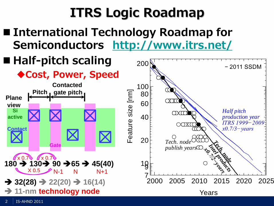
ITRS Logic Roadmap
International Technology Roadmap for Semiconductors http://www.itrs.net/
Half-pitch scaling
Cost, Power, Speed
2
Gate
Contact
Si
active
Pitch Contacted
gate pitch
180 130 90 65 45(40)
32(28) 22(20) 16(14)
11-nm technology node
x 0.7 x 0.7
X 0.5 N N+1 N-1
Plane
view
2000 2005 2010 2015 2020 20257
910
20
40
60
80100
200
Years
Fe
atu
re s
ize
[n
m]
Half pitchproduction yearITRS 1999−2009x0.7/3−years
Tech. nodepublish years
Tech. node
Intel products
x0.7/2−years
− 2011 SSDM
IS-AHND 2011
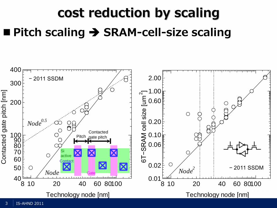
cost reduction by scaling
Pitch scaling SRAM-cell-size scaling
Gate
Contact
Si
active
Pitch Contacted
gate pitch
3
8 10 20 40 60 8010040
50
60708090
100
200
300
400
Technology node [nm]
Co
nta
cte
d g
ate
pitch
[n
m]
Node
Node0.5
− 2011 SSDM
8 10 20 40 60 801000.01
0.02
0.06
0.10
0.20
0.60
1.00
2.00
Technology node [nm]
6T
−S
RA
M c
ell
siz
e [u
m2]
Node2 − 2011 SSDM

IS-AHND 2011
10 nm, 0.021 um2, IBM, 11VL T4-5
The world smallest 6T-SRAM
FinFET u/ Mixed EB and Optical litho. (MXL)
Contacted gate pitch (CGP) scaling down to 50 nm
4
IS-AHND 2011
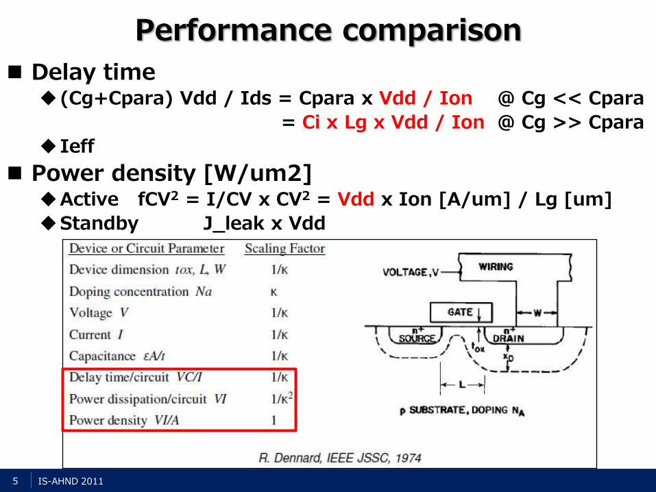
Performance comparison
Delay time (Cg+Cpara) Vdd / Ids = Cpara x Vdd / Ion @ Cg << Cpara
= Ci x Lg x Vdd / Ion @ Cg >> Cpara
Ieff
Power density [W/um2] Active fCV2 = I/CV x CV2 = Vdd x Ion [A/um] / Lg [um]
Standby J_leak x Vdd
5
IS-AHND 2011
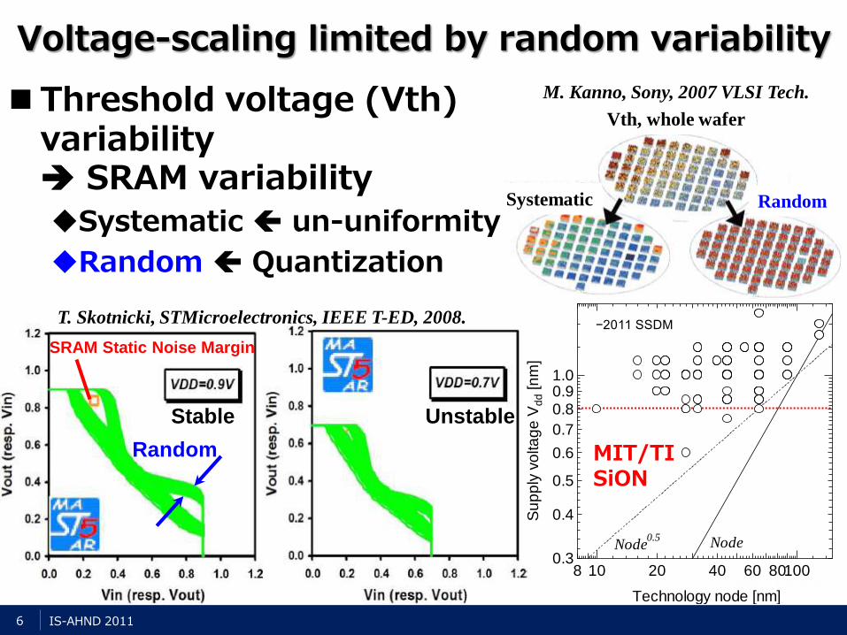
Voltage-scaling limited by random variability
Threshold voltage (Vth) variability SRAM variability
Systematic un-uniformity
Random Quantization
Stable Unstable
Systematic
T. Skotnicki, STMicroelectronics, IEEE T-ED, 2008.
Random
Vth, whole wafer
SRAM Static Noise Margin
Random
M. Kanno, Sony, 2007 VLSI Tech.
6
8 10 20 40 60 801000.3
0.4
0.5
0.6
0.7
0.80.91.0
Technology node [nm]
Su
pp
ly v
olta
ge
Vd
d [n
m]
Node0.5 Node
−2011 SSDM
MIT/TI SiON

IS-AHND 2011
28nm, 0.6 V SoC, MIT/TI, ISSCC11 7.5/14.4
Poly-Si/SiON, 6T-SRAM
3s, 0.6V
7
IS-AHND 2011
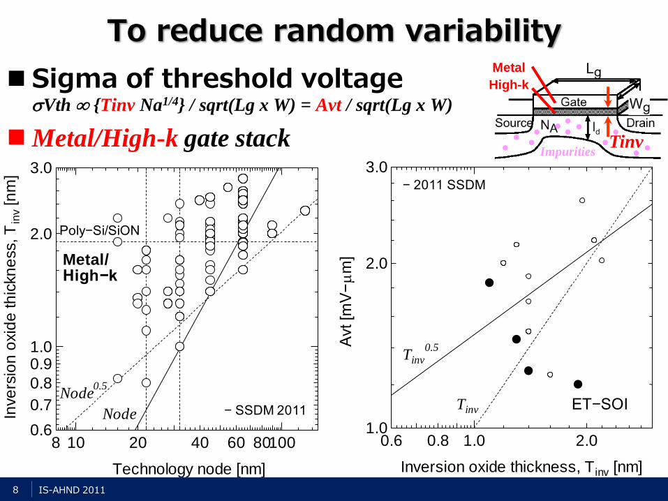
To reduce random variability
Sigma of threshold voltage sVth {Tinv Na1/4} / sqrt(Lg x W) = Avt / sqrt(Lg x W)
Metal/High-k gate stack Tinv Impurities
Metal
High-k
8
8 10 20 40 60 801000.6
0.7
0.8
0.91.0
2.0
3.0
Technology node [nm]
Inve
rsio
n o
xid
e th
ickn
ess, T
inv
[nm
]
Node0.5
Node − SSDM 2011
Poly−Si/SiON
Metal/High−k
0.6 0.8 1.0 2.01.0
2.0
3.0
Inversion oxide thickness, Tinv [nm]
Avt [m
V−
m
]Tinv
0.5
ET−SOITinv
− 2011 SSDM
IS-AHND 2011
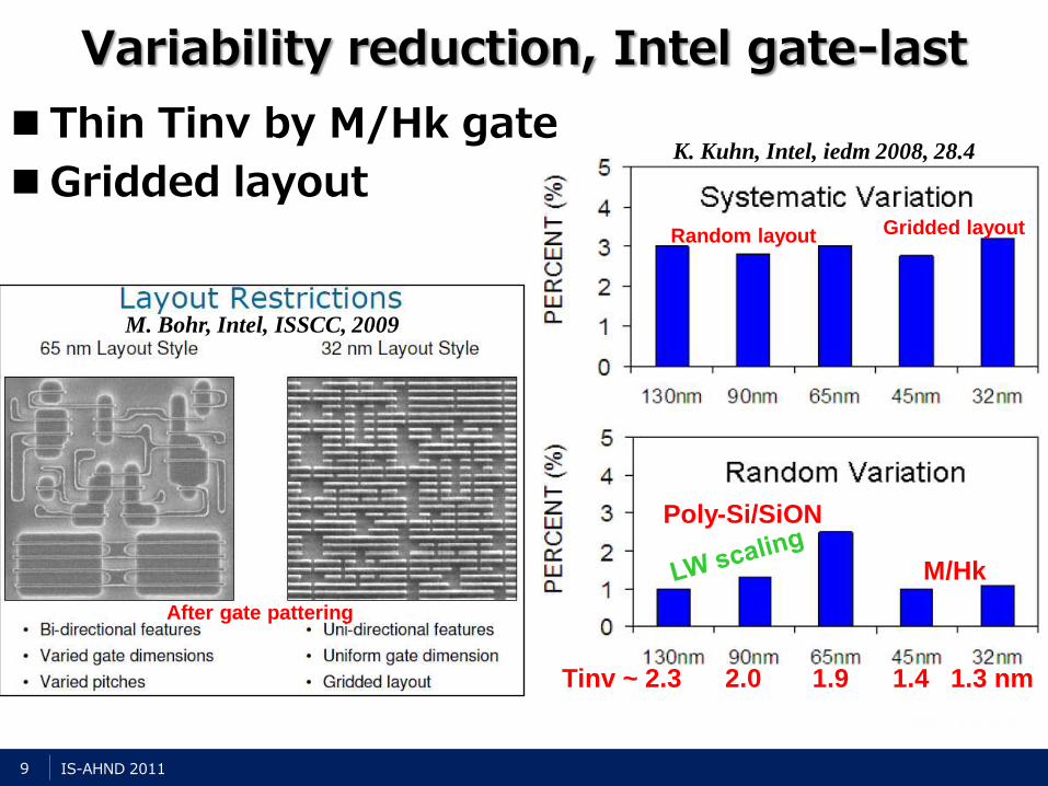
Variability reduction, Intel gate-last
Thin Tinv by M/Hk gate
Gridded layout
Tinv ~ 2.3 2.0 1.9 1.4 1.3 nm
M/Hk
Gridded layout
Poly-Si/SiON
Random layout
K. Kuhn, Intel, iedm 2008, 28.4
M. Bohr, Intel, ISSCC, 2009
After gate pattering
9
IS-AHND 2011
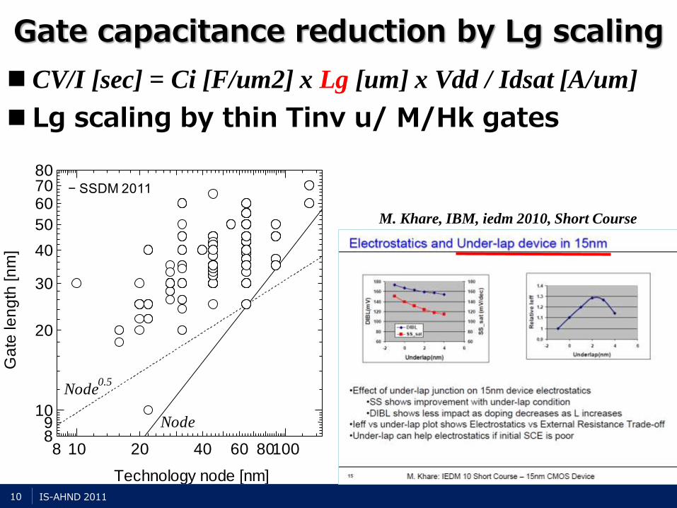
Gate capacitance reduction by Lg scaling
CV/I [sec] = Ci [F/um2] x Lg [um] x Vdd / Idsat [A/um]
Lg scaling by thin Tinv u/ M/Hk gates
M. Khare, IBM, iedm 2010, Short Course
10
8 10 20 40 60 8010089
10
20
30
40
50
607080
Technology node [nm]
Ga
te le
ng
th [n
m]
Node
Node0.5
− SSDM 2011
IS-AHND 2011
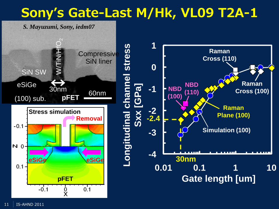
Sony’s Gate-Last M/Hk, VL09 T2A-1
11
-4
-3
-2
-1
0
1
0.01 0.1 1 10
Raman
Cross (110)
Raman
Cross (100)
Raman
Plane (100)
NBD
(100)
NBD
(110)
Simulation (100)
Gate length [um]
Lo
ng
itu
din
al c
han
ne
l s
tres
s
Sx
x [
GP
a]
-2.4
30nm
Stress simulation
eSiGe eSiGe
pFET
Removal
SiN SW
30nm 60nm
Compressive SiN liner
eSiGe
(100) sub.
W/T
iN/H
fO2
pFET
S. Mayuzumi, Sony, iedm07
IS-AHND 2011
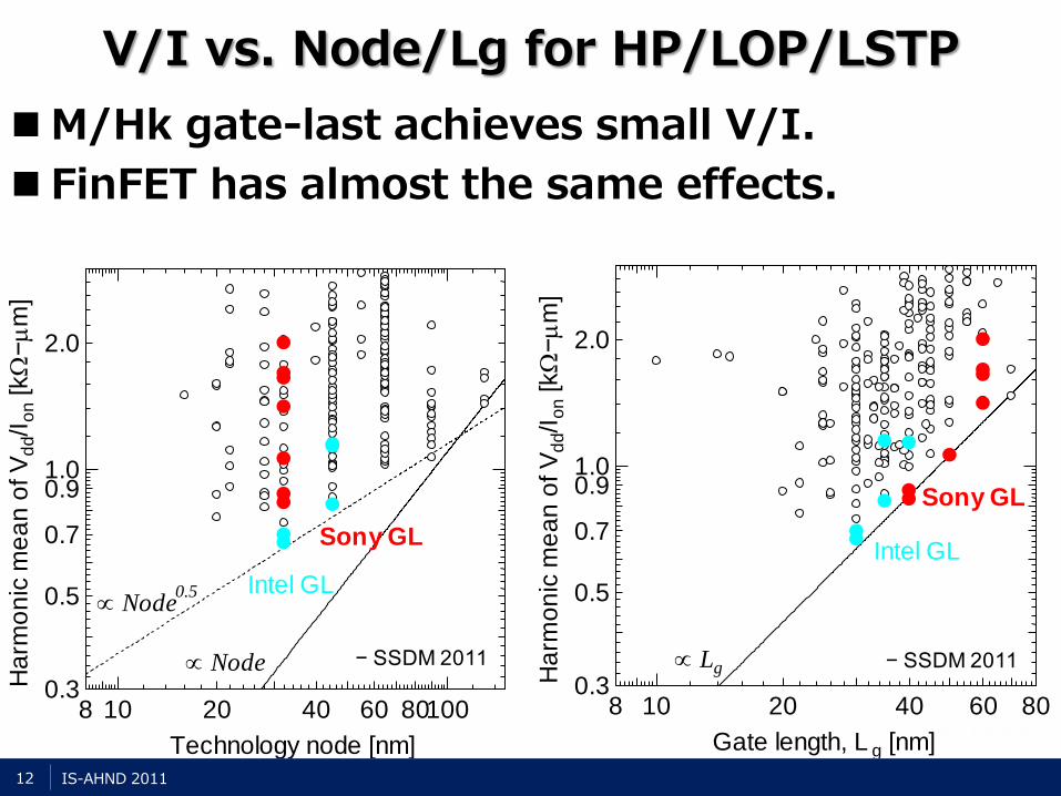
V/I vs. Node/Lg for HP/LOP/LSTP
M/Hk gate-last achieves small V/I.
FinFET has almost the same effects.
12
8 10 20 40 60 800.3
0.5
0.7
0.91.0
2.0
Gate length, L g [nm]
Ha
rmo
nic
me
an
of V
dd/I
on [k
−
m
]
Lg − SSDM 2011
Sony GL
Intel GL
8 10 20 40 60 801000.3
0.5
0.7
0.91.0
2.0
Technology node [nm]
Ha
rmo
nic
me
an
of V
dd/I
on [k
−
m
]
Node − SSDM 2011
Sony GL
Intel GL Node
0.5
IS-AHND 2011
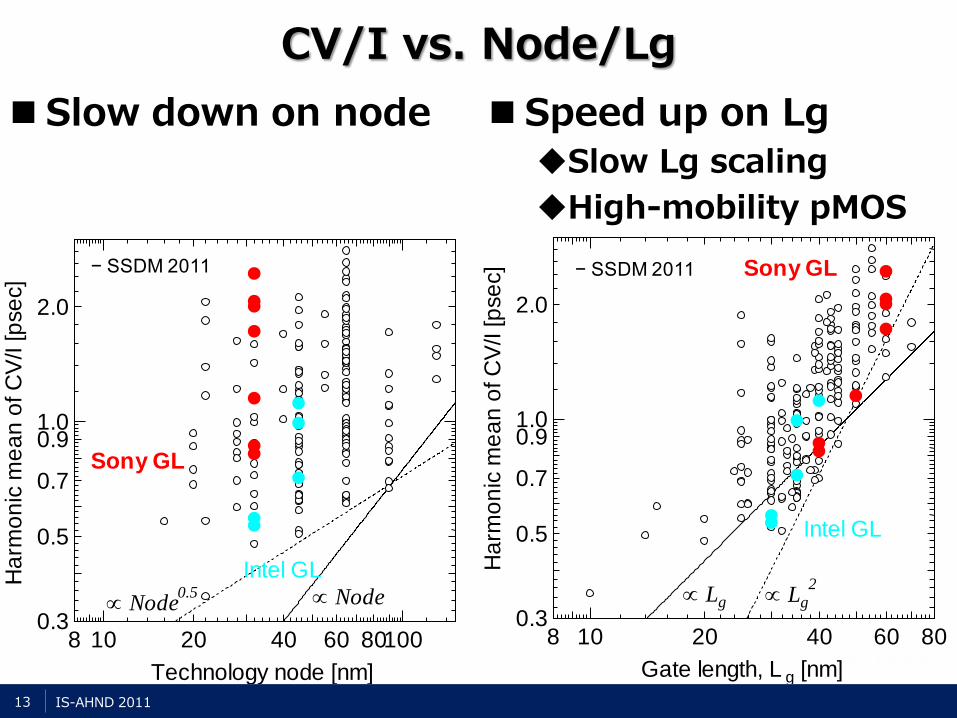
Slow down on node Speed up on Lg
Slow Lg scaling
High-mobility pMOS
CV/I vs. Node/Lg
13
8 10 20 40 60 801000.3
0.5
0.7
0.91.0
2.0
Technology node [nm]
Ha
rmo
nic
me
an
of C
V/I [p
se
c]
Node
− SSDM 2011
Sony GL
Intel GL
Node0.5
8 10 20 40 60 800.3
0.5
0.7
0.91.0
2.0
Gate length, L g [nm]
Ha
rmo
nic
me
an
of C
V/I [p
se
c]
Lg
− SSDM 2011 Sony GL
Intel GL
Lg
2
IS-AHND 2011
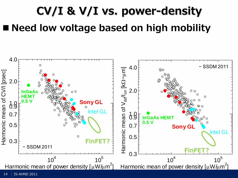
CV/I & V/I vs. power-density
Need low voltage based on high mobility
14
104
105
0.3
0.5
0.7
0.91.0
2.0
4.0
Harmonic mean of power density [W/m2]
Ha
rmo
nic
me
an
of V
dd/I
on [k
−
m
] − SSDM 2011
Sony GLIntel GL
InGaAs HEMT0.5 V
FinFET?
FinFET?
104
105
0.3
0.5
0.7
0.91.0
2.0
4.0
Harmonic mean of power density [ W/m2]
Ha
rmo
nic
me
an
of C
V/I [p
se
c]
− SSDM 2011
Sony GL
Intel GL
InGaAsHEMT0.5 V
IS-AHND 2011
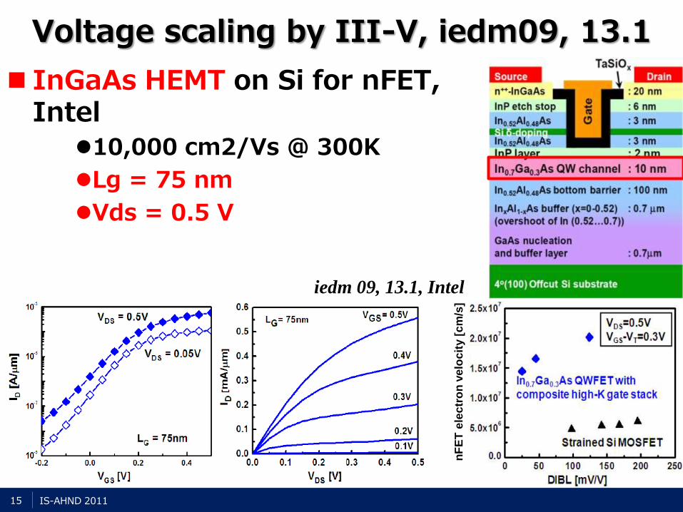
Voltage scaling by III-V, iedm09, 13.1
InGaAs HEMT on Si for nFET, Intel
10,000 cm2/Vs @ 300K
Lg = 75 nm
Vds = 0.5 V
iedm 09, 13.1, Intel
nF
ET
ele
ctr
on
ve
loc
ity [
cm
/s]
15
IS-AHND 2011
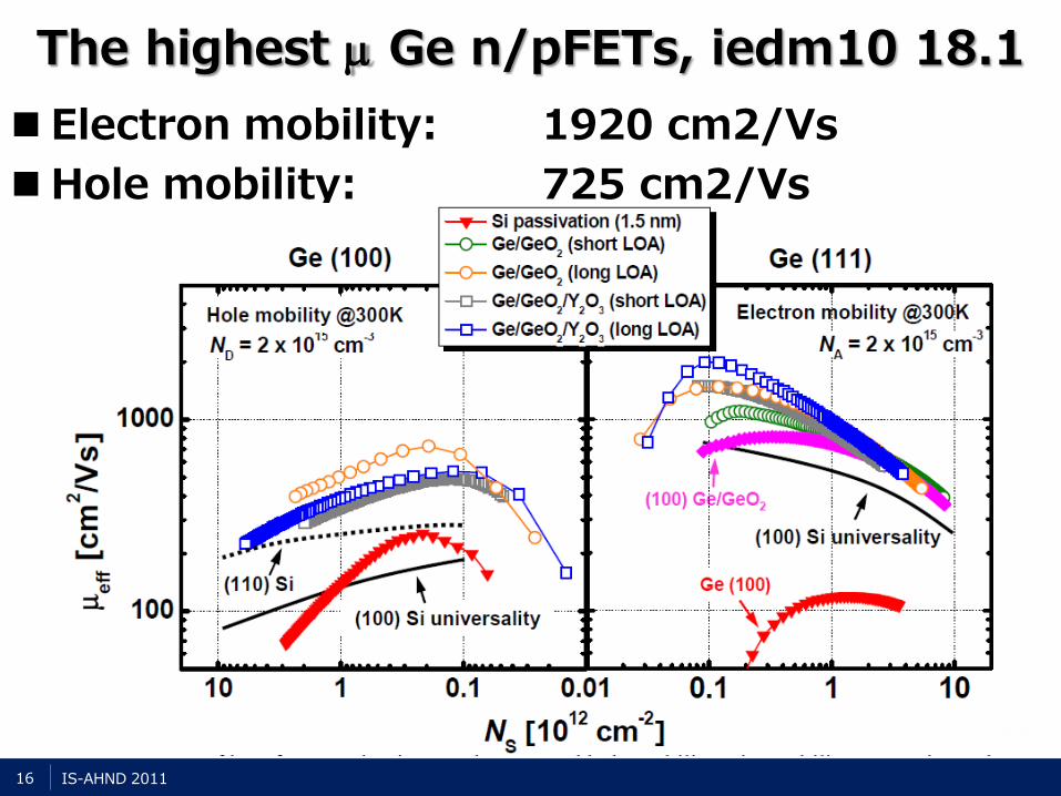
The highest Ge n/pFETs, iedm10 18.1
Electron mobility: 1920 cm2/Vs
Hole mobility: 725 cm2/Vs
16
IS-AHND 2011
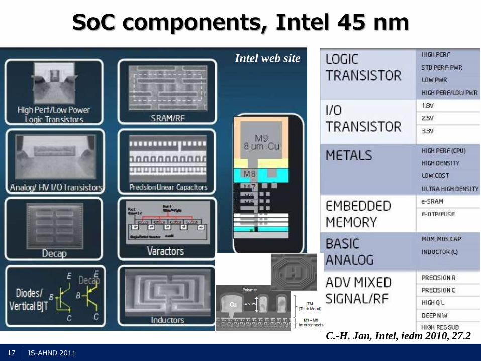
SoC components, Intel 45 nm
17
Intel web site
C.-H. Jan, Intel, iedm 2010, 27.2
IS-AHND 2011
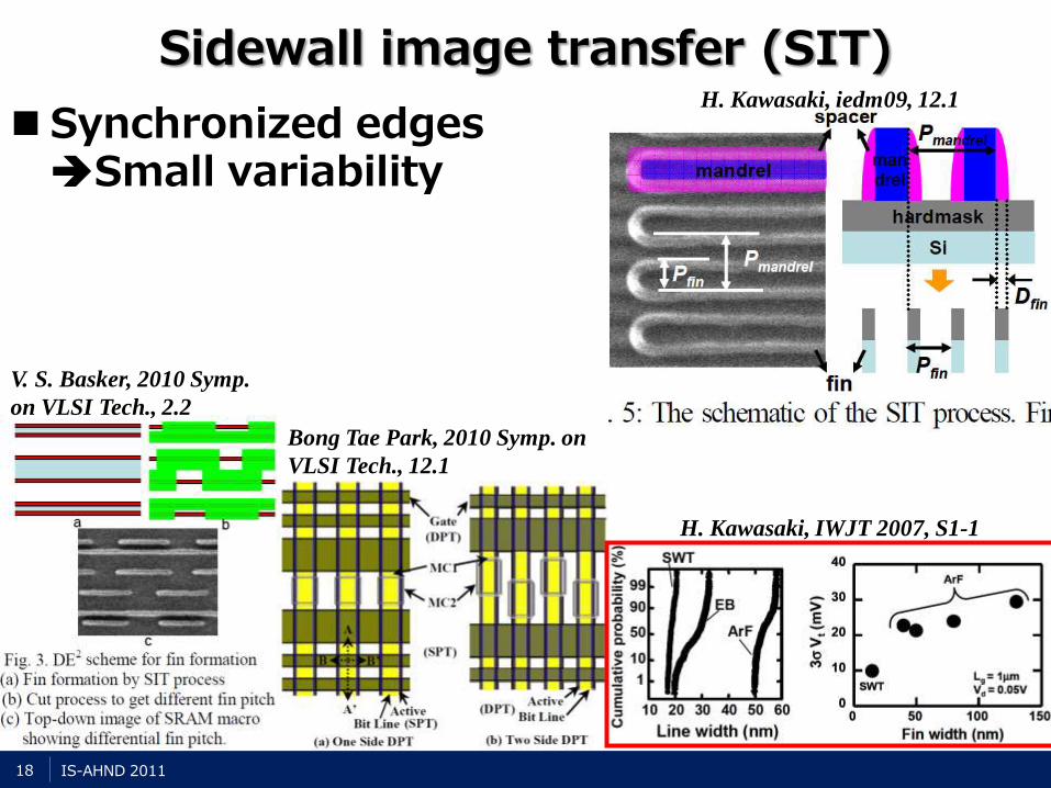
Sidewall image transfer (SIT)
Synchronized edges Small variability
H. Kawasaki, iedm09, 12.1
V. S. Basker, 2010 Symp.
on VLSI Tech., 2.2
Bong Tae Park, 2010 Symp. on
VLSI Tech., 12.1
H. Kawasaki, IWJT 2007, S1-1
18
IS-AHND 2011
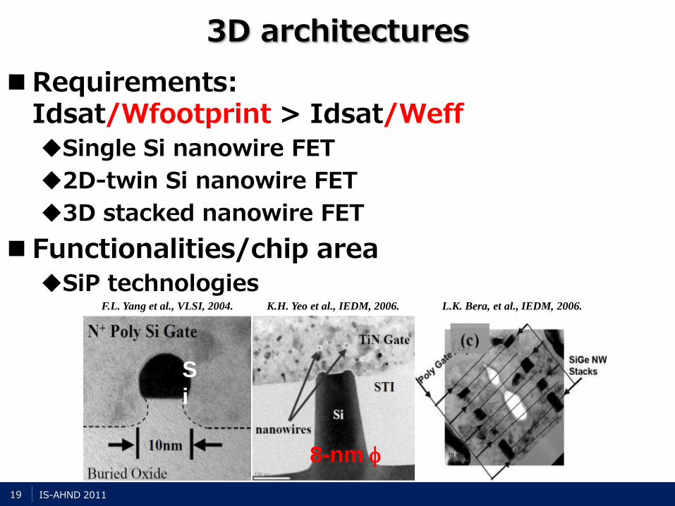
3D architectures
Requirements: Idsat/Wfootprint > Idsat/Weff
Single Si nanowire FET
2D-twin Si nanowire FET
3D stacked nanowire FET
Functionalities/chip area
SiP technologies F.L. Yang et al., VLSI, 2004.
S
i
L.K. Bera, et al., IEDM, 2006.
8-nm f
K.H. Yeo et al., IEDM, 2006.
19
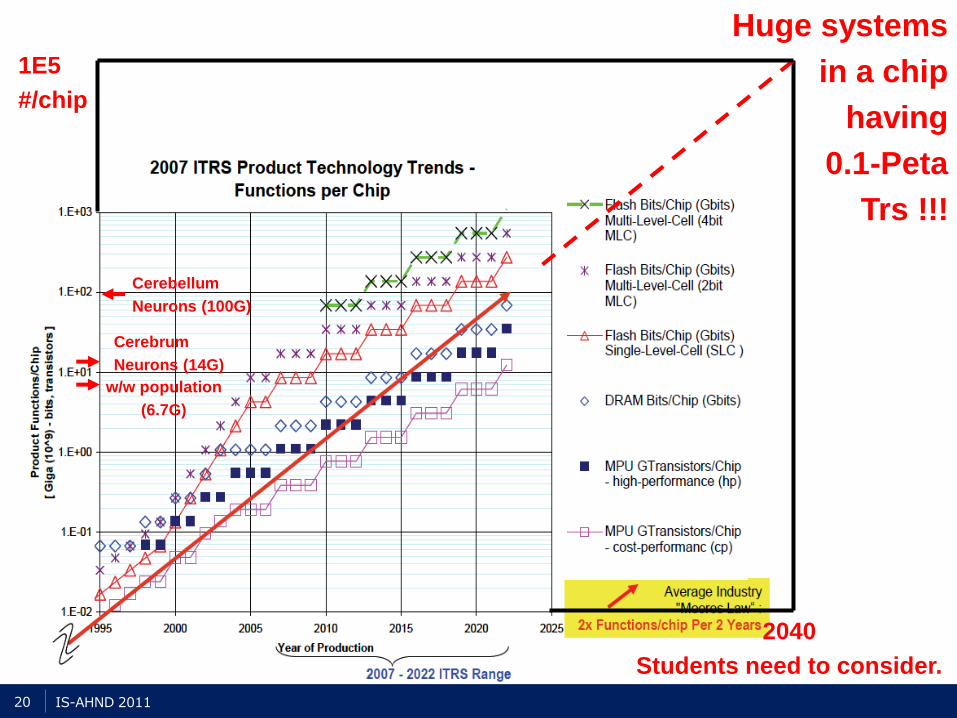
IS-AHND 2011
Huge systems
in a chip
having
0.1-Peta
Trs !!!
2040
Students need to consider.
w/w population
(6.7G)
Cerebrum
Neurons (14G)
1E5
#/chip
Cerebellum
Neurons (100G)
20
IS-AHND 2011
Summary
Benchmarks of CMOS scaling
Cost
Power
Speed
21


