chapter 3 cmos device modeling - university of rhode · pdf fileallen/holberg : chapter 3 :...
TRANSCRIPT

Allen/Holberg : Chapter 3 : 1/13/01 1
Chapter 3 CMOS Device ModelingBefore one can design a circuit to be integrated in CMOS technology, one must first
have a model describing the behavior of all the components available for use in thedesign. A model can take the form of mathematical equations, circuit representations, ortables. Most of the modeling used in this text will focus on the active and passive devicesdiscussed in the previous chapter as opposed to higher-level modeling such asmacromodeling, or behavioral modeling.
It should be stressed at the outset that a model is just that and no more—it is not thereal thing! In an ideal world, we would have a model that accurately describes thebehavior of a device under all possible conditions. Realistically, we are happy to have amodel that predicts simulated performance to within a few percent of measuredperformance. There is no clear agreement as to which model comes closest to meetingthis “ideal” model [1]. This lack of agreement is illustrated by the fact that, at thiswriting, HSPICE [25] offers the user 43 different MOS transistor models from which tochoose!
This text will concentrate only three of these models. The simplest model which isappropriate for hand calculations was described in Sec 2.3 and will be further developedhere to include capacitance, noise, and ohmic resistance. In SPICE terminology, thissimple model is called the LEVEL 1 model. Next, a small-signal model is derived fromthe LEVEL 1 large-signal model and is presented in Sec. 3.3.
A far more complex model, the SPICE LEVEL 3 model is presented in Sec. 3.4.This model includes many effects that are more evident in modern short-channeltechnologies as well as subthreshold conduction. It is adequate for device geometriesdown to about 0.8µm. Finally, the BSIM3v3 model is presented. This model is theclosest to becoming a standard for computer simulation.
NotationSPICE was originally implemented in FORTRAN where all input was required to be
uppercase ASCII characters. Lowercase, greek, and super/subscripting were not allowed.Modern SPICE implementations generally accept (but do not distinguish between) upper-and lowercase but the tradition of using uppercase ASCII still lives on. This isparticularly evident in the device model parameters. Since greek characters are notavailable, these were simply spelled out, e.g., γ entered as GAMMA. Super andsubscripts were simply not used.
It is inconvenient to adopt the SPICE naming convention throughout the bookbecause equations would appear unruly and would not be familiar to what is commonlyseen in the literature. On the other hand, it is necessary to provide the correct notationwhere application to SPICE is intended. To address this dilemma, we have decided touse SPICE uppercase (non italic) notation for all model parameters except those appliedto the simple model (SPICE LEVEL 1).
3.1 Simple MOS Large-SignalAll large-signal models will be developed for the n-channel MOS device with the
positive polarities of voltages and currents shown in Fig. 3.1-1(a). The same models canbe used for the p-channel MOS device if all voltages and currents are multiplied by −1and the absolute value of the p-channel threshold is used. This is equivalent to using thevoltages and currents defined by Fig. 3.1-1(b) which are all positive quantities. As

Allen/Holberg : Chapter 3 : 1/13/01 2
mentioned in Chapter 1, lower-case variables with capital subscripts will be used for thevariables of large-signal models and lower-case variables with lower-case subscripts willbe used for the variables of small-signal models. When the voltage or current is a modelparameter, such as threshold voltage, it will be designated by an upper-case variable andan upper-case subscript.
(a) (b)
B
D
S
G vDS
vBSvGS
iD
+
-
+
-
B
D
S
G vSD
vSBvSG
iD
-
+
-
+
Figure 3.1-1 Positive sign convention for (a) n-channel, and (b) p-channel MOS transistor.
When the length and width of the MOS device is greater than about 10 µm, thesubstrate doping is low, and when a simple model is desired, the model suggested bySah [2] and used in SPICE by Shichman and Hodges [3] is very appropriate. This modelwas developed in Eq. (28) of Sec. 2.3 and given below.
iD = µoCoxW
L
(vGS − VT) −
vDS
2 vDS (1)
The terminal voltages and currents have been defined in the previous chapter. Thevarious parameters of (1) are defined as
µo = surface mobility of the channel for the n-channel or p-channel device (cm2/V-s)
Cox = εoxtox
= capacitance per unit area of the gate oxide (F/cm2)
W = effective channel width
L = effective channel length
The threshold voltage VT is given by Eq. (19) of Sec. 2.3 for an n-channel transistor
VT = VT0 + γ 2|φF| + vSB − 2|φF| (2)
VT0 = VT (vSB = 0) = VFB + 2|φF| + 2qεsi NSUB 2|φF|
Cox(3)
γ = bulk threshold parameter (V1/2) = 2εsi q NSUB
Cox(4)
Allen/Holberg : Chapter 3 : 1/13/01 3
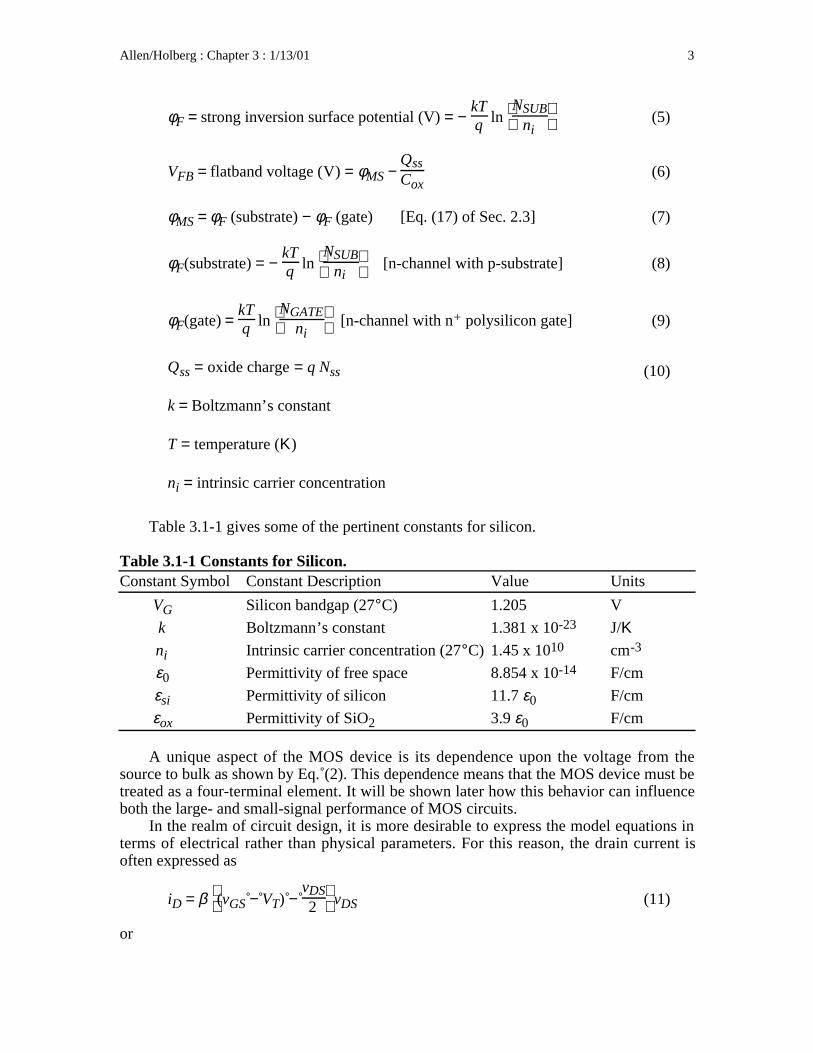
φF = strong inversion surface potential (V) = − kTq ln
NSUB
ni(5)
VFB = flatband voltage (V) = φMS − QssCox
(6)
φMS = φF (substrate) − φF (gate) [Eq. (17) of Sec. 2.3] (7)
φF(substrate) = − kTq ln
NSUB
ni [n-channel with p-substrate] (8)
φF(gate) = kTq ln
NGATE
ni [n-channel with n+ polysilicon gate] (9)
Qss = oxide charge = q Nss (10)
k = Boltzmann’s constant
T = temperature (Κ)
ni = intrinsic carrier concentration
Table 3.1-1 gives some of the pertinent constants for silicon.
Table 3.1-1 Constants for Silicon.Constant Symbol Constant Description Value Units
VG Silicon bandgap (27°C) 1.205 V
k Boltzmann’s constant 1.381 x 10⁻²³ J/Κni Intrinsic carrier concentration (27°C) 1.45 x 1010 cm-3
ε0 Permittivity of free space 8.854 x 10⁻¹⁴ F/cm
εsi Permittivity of silicon 11.7 ε0 F/cm
εox Permittivity of SiO2 3.9 ε0 F/cm
A unique aspect of the MOS device is its dependence upon the voltage from thesource to bulk as shown by Eq. (2). This dependence means that the MOS device must betreated as a four-terminal element. It will be shown later how this behavior can influenceboth the large- and small-signal performance of MOS circuits.
In the realm of circuit design, it is more desirable to express the model equations interms of electrical rather than physical parameters. For this reason, the drain current isoften expressed as
iD = β
(vGS − VT) −
vDS2 vDS (11)
or
Allen/Holberg : Chapter 3 : 1/13/01 4
iD = K' WL
(vGS − VT) −
vDS2 vDS (12)
where the transconductance parameter β is given in terms of physical parameters as
β = (K' ) WL ≅ (µoCox)
WL (A/V2) (13)
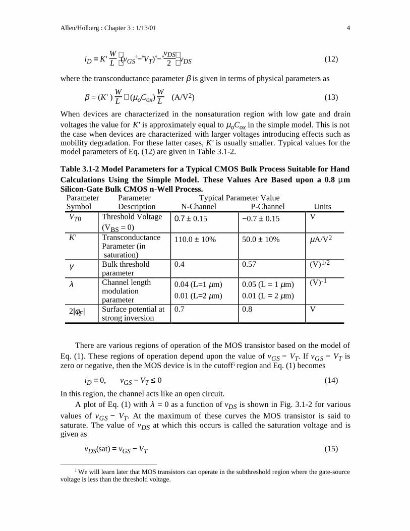
When devices are characterized in the nonsaturation region with low gate and drainvoltages the value for K' is approximately equal to µoCox in the simple model. This is notthe case when devices are characterized with larger voltages introducing effects such asmobility degradation. For these latter cases, K' is usually smaller. Typical values for themodel parameters of Eq. (12) are given in Table 3.1-2.
Table 3.1-2 Model Parameters for a Typical CMOS Bulk Process Suitable for HandCalculations Using the Simple Model. These Values Are Based upon a 0.8 µmSilicon-Gate Bulk CMOS n-Well Process.
Parameter Parameter Typical Parameter ValueSymbol Description N-Channel P-Channel UnitsVT0 Threshold Voltage
(VBS = 0)0.7 ± 0.15 −0.7 ± 0.15 V
K' TransconductanceParameter (in saturation)
110.0 ± 10% 50.0 ± 10% µA/V2
γ Bulk thresholdparameter
0.4 0.57 (V)1/2
λ Channel lengthmodulationparameter
0.04 (L=1 µm)
0.01 (L=2 µm)
0.05 (L = 1 µm)
0.01 (L = 2 µm)
(V)-1
2|φF| Surface potential atstrong inversion
0.7 0.8 V
There are various regions of operation of the MOS transistor based on the model ofEq. (1). These regions of operation depend upon the value of vGS − VT. If vGS − VT iszero or negative, then the MOS device is in the cutoffi region and Eq. (1) becomes
iD = 0, vGS − VT ≤ 0 (14)
In this region, the channel acts like an open circuit.A plot of Eq. (1) with λ = 0 as a function of vDS is shown in Fig. 3.1-2 for various
values of vGS − VT. At the maximum of these curves the MOS transistor is said tosaturate. The value of vDS at which this occurs is called the saturation voltage and isgiven as
vDS(sat) = vGS − VT (15)
i We will learn later that MOS transistors can operate in the subthreshold region where the gate-source
voltage is less than the threshold voltage.

Allen/Holberg : Chapter 3 : 1/13/01 5
0
vDS = vGS − VT
vDS
vGS
Increasing
iD
Figure 3.1-2 Graphical illustration of the modified Sah equation.
Thus, vDS(sat) defines the boundary between the remaining two regions of operation. IfvDS is less than vDS(sat), then the MOS transistor is in the nonsaturated region and Eq. (1)becomes
iD = (K' ) WL
(vGS − VT) −
vDS2 vDS ; 0 < vDS ≤ (vGS − VT) (16)
In Fig. 3.1-2, the nonsaturated region lies between the vertical axis (vDS = 0) and vDS =vGS − VT curve.
The third region occurs when vDS is greater than vDS(sat) or vGS − VT. At this pointthe current iD becomes independent of vDS. Therefore, vDS in Eq. (1) is replaced byvDS(sat) of Eq. (11) to get
iD = K' W2L (vGS − VT)2, 0 < (vGS − VT) ≤ vDS (17)
Equation (17) indicates that drain current remains constant once vDS is greater thanvGS − VT. In reality, this is not true. As drain voltage increases, the channel length isreduced resulting in increased current. This phenomenon is called channel lengthmodulation and is accounted for in the saturation model with the addition of the factor,(1 + λvDS) where vDS is the actual drain-source voltage and not vDS(sat). The saturationregion model modified to include channel-length modulation is given in Eq. (18)
iD = K' W2L (vGS − VT)2(1 + λvDS), 0 < (vGS − VT) ≤ vDS (18)
The output characteristics of the MOS transistor can be developed from Eqs. (14),(16), and (18). Figure 3.1-3 shows these characteristics plotted on a normalized basis.These curves have been normalized to the upper curve where VGS0 is defined as the valueof vGS which causes a drain current of ID0 in the saturation region. The entirecharacteristic is developed by extending the solid curves of Fig. 3.1-2 horizontally to the

Allen/Holberg : Chapter 3 : 1/13/01 6
right from the maximum points. The solid curves of Fig. 3.1-3 correspond to λ = 0. If
λ ≠ 0, then the curves are the dashed lines.
0
iD / ID0
Figure 3.1-3 Output characteristics of the MOS device.
vDS / (VGS0 − VT)
vDS = vGS − VTvGS − VT
VGS0 − VT
= 1.00
vGS − VT
VGS0 − VT
= 0.867
vGS − VT
VGS0 − VT
= 0.707
vGS − VT
VGS0 − VT
= 0.50
Channel-length modulation effects
vGS − VT
VGS0 − VT
= 0.00Cutoff region
0.25
0.50
0.75
1.00
0.5 1.0 2.0 2.5
Another important characteristic of the MOS transistor can be obtained by plottingiD versus vGS using Eq. (18). Fig. 3.1-4 shows this result. This characteristic of the MOStransistor is called the transconductance characteristic. We note that the transconductancecharacteristic in the saturation region can be obtained from Fig. 3.1-3 by drawing avertical line to the right of the parabolic dashed line and plotting values of iD versus vGS.Fig. 3.1-4 is also useful for illustrating the effect of the source-bulk voltage, vSB. As thevalue of vSB increases, the value of VT increases for the enhancement, n-channel devices(for a p-channel device, |VT| increases as vBS increases). VT also increases positively forthe n-channel depletion device, but since VT is negative, the value of VT approaches zerofrom the negative side. If vSB is large enough, VT will actually become positive and thedepletion device becomes an enhancement device.

Allen/Holberg : Chapter 3 : 1/13/01 7
0
vDS ≥ vGS − VT
vGS
vSB3 > vSB2 > vSB1 > 0
iD
Figure 3.1-4 Transconductance characteristic of the MOS transistor as a function of the bulk-source voltage, vSB.
Since the MOS transistor is a bidirectional device, determining which physical nodeis the drain and which the source may seem arbitrary. This is not really the case. For an n-channel transistor, the source is always at the lower potential of the two nodes. For the p-channel transistor, the source is always at the higher potential. It is obvious that the drainand source designations are not constrained to a given node of a transistor but can switchback and forth depending upon the terminal voltages applied to the transistor.
A circuit version of the large-signal model of the MOS transistor consists of acurrent source connected between the drain and source terminals, that depends on thedrain, source, gate, and bulk terminal voltages defined by the simple model described inthis section. This simple model has five electrical and process parameters that completelydefine it. These parameters are K', VT, γ, λ , and 2φF. The subscript n or p will be usedwhen the parameter refers to an n-channel or p-channel device, respectively. Theyconstitute the Level I model parameters of SPICE [23]. Typical values for these modelparameters are given in Table 3.1-2.
The function of the large-signal model is to solve for the drain current given theterminal voltages of the MOS device. An example will help to illustrate this as well asshow how the model is applied to the p-channel device.
Example 3.1-1Application of the Simple MOS Large Signal Model
Assume that the transistors in Fig. 3.1-1 have a W/L ratio of 5 µm/1 µm and that thelarge signal model parameters are those given in Table 3.1-2. If the drain, gate, source,and bulk voltages of the n-channel transistor is 3 V, 2 V, 0 V, and 0 V, respectively, findthe drain current. Repeat for the p-channel transistor if the drain, gate, source, and bulkvoltages are −3 V, −2 V, 0 V, and 0 V, respectively.
We must first determine in which region the transistor is operating. Eq. (15) givesvDS(sat) as 2 V − 0.7 V = 1.3 V. Since vDS is 3 V, the n-channel transistor is in thesaturation region. Using Eq. (18) and the values from Table 3.1-2 we have
iD = K'NW
2L (vGS − VTN)2(1 + λN vDS)

Allen/Holberg : Chapter 3 : 1/13/01 8
= 110 × 10−6(5 µm)
2(1 µm) (2 − 0.7)2(1 + 0.04 × 3) = 520 µA
Evaluation of Eq. (15) for the p-channel transistor is given as
vSD(sat) = vSG − |VTP| = 2 V − 0.7 V = 1.3 V
Since vSD is 3 V, the p-channel transistor is also in the saturation region, Eq. (17) isapplicable. The drain current of Fig. 3.1-1(b) can be found using the values from Table3.1-2 as
iD = K'PW
2L (vSG − |VTP| )2(1 + λP vSD)
= 50 × 10−6(5 µm)
2(1 µm) (2 − 0.7)2(1 + 0.05 × 3) = 243 µΑ
It is often useful to describe vGS in terms of iD in saturation as shown below.
vGS = VT + 2iDβ
(19)
This expressions illustrates that there are two components to vGS —an amount to invertthe channel plus an additional amount to support the desired drain current. This secondcomponent is often referred to in the literature as VON. Thus VON can be defined as
VON = 2iDβ
(20)
The term VON should be recognized as the term for saturation voltage VDS (sat). Theycan be used interchangeably.
3.2 Other MOS Large-Signal Model ParametersThe large-signal model also includes several other characteristics such as the
source/drain bulk junctions, source/drain ohmic resistances, various capacitors, and noise.The complete version of the large-signal model is given in Fig. 3.2-1.

Allen/Holberg : Chapter 3 : 1/13/01 9
B
D
S
GiBD
iBS
vBS
vBD
CBDCGD
CGS
CGB
iD
rD
rS
CBS
Figure 3.2-1 Complete large-signal model for the MOS transistor.
The diodes of Fig. 3.2-1 represent the pn junctions between the source and substrateand the drain and substrate. For proper transistor operation, these diodes must always bereverse biased. Their purpose in the dc model is primarily to model leakage currents.These currents are expressed as
iBD = Is
exp
qvBD
kT −1 (1)
and
iBS = Is
exp
qvBS
kT −1 (2)
where Is is the reverse saturation current of a pn junction, q is the charge of an electron, kis Boltzmann’s constant, and T is temperature in Kelvin units.
The resistors rD and rS represent the ohmic resistance of the drain and source,respectively. Typically, these resistors may be 50 to 100 ohmsi and can often be ignoredat low drain currents.
The capacitance of Fig. 3.2-1 can be separated into three types. The first typeincludes capacitors CBD and CBS which are associated with the back-biased depletionregion between the drain and substrate and the source and substrate. The second typeincludes capacitors CGD, CGS, and CGB which are all common to the gate and are
i For a silicide process, these resistances will be much less—on the order of 5 to 10 ohms.

Allen/Holberg : Chapter 3 : 1/13/01 10
dependent upon the operating condition of the transistor. The third type includes parasiticcapacitors which are independent of the operating conditions.
The depletion capacitors are a function of the voltage across the pn junction. Theexpression of this junction-depletion capacitance is divided into two regions to accountfor the high injection effects. The first is given as
CBX = (CJ) (AX)
1 −
vBXPB
−MJ, vBX ≤ (FC)(PB) (3)
where
X = D for CBD or X = S for CBS
AX = area of the source (X = S) or drain (X = D)
CJ = zero-bias (vBX = 0) junction capacitance (per unit area)
CJ ≅ qεsiNSUB
2PB
PB = bulk junction potential (same as φo given in Eq. (6), sec. 2.2)
FC = forward-bias nonideal junction-capacitance coefficient (≅ 0.5)
MJ = bulk-junction grading coefficient (1/2 for step junctions and 1/3 for gradedjunctions)
The second region is given as
CBX = (CJ)(AX)
(1 − FC)1+MJ
1 − (1 + MJ)FC + MJ
vBXPB , vBX > (FC)(PB) (4)
Fig. 3.2-2 illustrates how the junction-depletion capacitances of Eqs. (3) and (4) arecombined to model the large signal capacitances CBD and CBS. It is seen that Eq. (4)prevents CBX from approaching infinity as vBX approaches PB.

Allen/Holberg : Chapter 3 : 1/13/01 11
0 vBX
Figure 3.2-2 Example of the method of modeling the voltage dependence of the bulk junction capacitances.
CBX0
CBX
Eq. (3)
Eq. (4)
(FC)(PB) PB
A closer examination of the depletion capacitors in Fig. 3.2-3 shows that thiscapacitor is like a tub. It has a bottom with an area equal to the area of the drain orsource. However, there are the sides that are also part of the depletion region. This area iscalled the sidewall. ABX in Eqs. (3) and (4) should include both the bottom and sidewallassuming the zero-bias capacitances of the two regions are similar. To more closelymodel the depletion capacitance, break it into the bottom and sidewall components, givenas follows.
CBX = (CJ)(AX)
1 −
vBX
PBMJ +
(CJSW)(PX)
1 −
vBX
PBMJSW , vBX ≤ (FC)(PB) (5)
and
CBX = (CJ)(AX)
(1 − FC)1+MJ
1 − (1 + MJ)FC + MJ
vBXPB
+ (CJSW)(PX)
(1 − FC)1+MJSW
1 − (1 + MJSW)FC +
vBXPB (MJSW) ,
vBX ≥ (FC)(PB) (6)
where
AX = area of the source (X = S) or drain (X = D)
PX = perimeter of the source (X = S) or drain (X = D)
CJSW = zero-bias, bulk-source/drain sidewall capacitance
MJSW = bulk-source/drain sidewall grading coefficient

Allen/Holberg : Chapter 3 : 1/13/01 12
Figure 3.2-3 Illustration showing the bottom and sidewall components of the bulk junction capacitors.
SiO2
Polysilicon gate
Bulk
A B
CD
EF
GH
Drain bottom = ABCD Drain sidewall = ABFE + BCGF + DCGH + ADHE
Source Drain
Table 3.2-1 gives the values for CJ, CJSW, MJ , and MJSW for an MOS devicewhich has an oxide thickness of 140 Å resulting in a Cox = 24.7 × 10⁻⁴ F/m2. It can beseen that the depletion capacitors cannot be accurately modeled until the geometry of thedevice is known, e.g., the area and perimeter of the source and drain. However, valuescan be assumed for the purpose of design. For example, one could consider a typicalsource or drain to be 1.8 µm by 5 µm. Thus a value for CBX of 2.9 fF and 6.9 fF results,
for n-channel and p-channel devices respectively, for VBX = 0.The large-signal, charge-storage capacitors of the MOS device consist of the gate-to-
source (CGS), gate-to-drain (CGD), and gate-to-bulk (CGB) capacitances. Figure 3.2-4shows a cross section of the various capacitances that constitute the charge-storagecapacitors of the MOS device. CBS and CBD are the source-to-bulk and drain-to-bulkcapacitors discussed above. The following discussion represents a heuristic developmentof a model for the large-signal charge-storage capacitors.

Allen/Holberg : Chapter 3 : 1/13/01 13
Figure 3.2-4 Large-signal, charge-storage capacitors of the MOS device.
SiO2
Bulk
Source Drain
Gate
CBSCBD
C4
C1 C2 C3
Table 3.2-1 Capacitance Values and Coefficients for the MOS Model.Type P-Channel N-Channel UnitsCGSO 220 × 10−12 220 × 10−12 F/m
CGDO 220 × 10−12 220 × 10−12 F/m
CGBO 700 × 10−12 700 × 10−12 F/m
CJ 560 × 10−6 770 × 10−6 F/m2
CJSW 350 × 10−12 380 × 10−12 F/m
MJ 0.5 0.5MJSW 0.35 0.38
Based on an oxide thickness of 140 Å or Cox=24.7 × 10⁻⁴ F/m2.
C1 and C3 are overlap capacitances and are due to an overlap of two conductingsurfaces separated by a dielectric. The overlapping capacitors are shown in more detail inFig. 3.2-5. The amount of overlap is designated as LD. This overlap is due to the lateraldiffusion of the source and drain underneath the polysilicon gate. For example, a 0.8 µmCMOS process might have a lateral diffusion component, LD, of approximately 16 nm.The overlap capacitances can be approximated as
C1 = C3 ≅ (LD)(Weff)Cox = (CGXO)Weff (7)
where Weff is the effective channel width and CGXO (X = S or D) is the overlapcapacitance in F/m for the gate-source or gate-drain overlap. The difference between themask W and actual W is due to the encroachment of the field oxide under the siliconnitride. Table 3.2-1 gives a value for CGSO and CGDO based on a device with an oxidethickness of 140 Å. A third overlap capacitance that can be significant is the overlapbetween the gate and the bulk. Fig. 3.2-6 shows this overlap capacitor (C5) in more detail.This is the capacitance that occurs between the gate and bulk at the edges of the channeland is a function of the effective length of the channel, Leff. Table 3.2-1 gives a typicalvalue for CGBO for a device based on an oxide thickness of 140 Å.

Allen/Holberg : Chapter 3 : 1/13/01 14
Figure 3.2-5 Overlap capacitances of an MOS transistor. (a) Top view showing the overlap between the source or drain and the gate. (b) Side view.
Bulk
LDMask
W
Oxide encroachment
ActualL (Leff)
Gate
Mask L
Source-gate overlap capacitance CGS (C1)
Drain-gate overlap capacitance CGD (C3)
Source Drain
Gate
FOX FOX
ActualW (Weff)
The channel of Fig. 3.2-4 is shown for the saturated state and would extendcompletely to the drain if the MOS device were in the nonsaturated state. C2 is the gate-to-channel capacitance and is given as
C2 = Weff(L − 2LD)Cox = Weff(Leff)Cox (8)
The term Leff is the effective channel length resulting from the mask-defined length beingreduced by the amount of lateral diffusion (note that up until now, the symbols L and Wwere used to refer to “effective” dimensions whereas now these have been changed foradded clarification). C4 is the channel-to-bulk capacitance which is a depletioncapacitance that will vary with voltage like CBS or CBD.
It is of interest to examine CGB, CGS, and CGD as vDS is held constant and vGS isincreased from zero. To understand the results, one can imagine following a vertical lineon Fig. 3.1-3 at say, vDS = 0.5(VGS0 − VT), as vGS increases from zero. The MOS devicewill first be off until vGS reaches VT. Next, it will be in the saturated region until vGSbecomes equal to vDS(sat) + VT. Finally, the MOS device will be in the nonsaturatedregion. The approximate variation of CGB, CGS, and CGD under these conditions isshown in Fig. 3.2-7. In cutoff, there is no channel and CGB is approximately equal toC2 + 2C5. As vGS approaches VT from the off region, a thin depletion layer is formed,creating a large value of C4. Since C4 is in series with C2, little effect is observed. As vGSincreases, this depletion region widens, causing C4 to decrease and reducing CGB. WhenvGS = VT, an inversion layer is formed which prevents further decreases of C4 (and thusCGB).

Allen/Holberg : Chapter 3 : 1/13/01 15
Figure 3.2-6 Gate-bulk overlap capacitances.
Bulk
Overlap Overlap
Source/Drain
GateFOX FOX
C5 C5
C1, C2, and C3 constitute CGS and CGD. The problem is how to allocate C2 to CGSand CGD. The approach used is to assume in saturation that approximately 2/3 of C2belongs to CGS and none to CGD. This is, of course, an approximation. However, it hasbeen found to give reasonably good results. Fig. 3.2-7 shows how CGS and CGD changevalues in going from the off to the saturation region. Finally, when vGS is greater thanvDS + VT, the MOS device enters the nonsaturated region. In this case, the channelextends from the drain to the source and C2 is simply divided evenly between CGD andCGS as shown in Fig. 3.2-7.
0 vGS
Figure 3.2-7 Voltage dependence of CGS, CGD, and CGB as a function of VGSwith VDS constang and VBS = 0.
CGS
CGS, CGD
CGD
CGB
CGS, CGD
C2 + 2C5
C1 +23_C2
C1 +12_C2
C1, C3
2C5
VT vDS +VT
Off SaturationNon-
Saturation
vDS = constant vBS = 0
Capacitance
As a consequence of the above considerations, we shall use the following formulasfor the charge-storage capacitances of the MOS device in the indicated regions.
Off
CGB = C2 + 2C5 = Cox(Weff)(Leff) + 2CGBO(Leff) (9a)
CGS = C1 ≅ Cox(LD)(Weff) = CGSO(Weff) (9b)
CGD = C3 ≅ Cox(LD)(Weff) = CGDO(Weff) (9c)
Saturation

Allen/Holberg : Chapter 3 : 1/13/01 16
CGB = 2C5 = CGBO (Leff) (10a)
CGS = C1 + (2/3)C2 = Cox(LD + 0.67Leff)(Weff)
= CGSO(Weff) + 0.67Cox(Weff)(Leff) (10b)
CGD = C3 ≅ Cox(LD)(Weff) = CGDO(Weff) (10c)
Nonsaturated
CGB = 2C5 = CGBO (Leff) (11a)
CGS = C1 + 0.5C2 = Cox(LD + 0.5Leff)(Weff)
= (CGSO + 0.5CoxLeff)Weff (11b)
CGD = C3 + 0.5C2 = Cox(LD + 0.5Leff)(Weff)
= (CGDO + 0.5CoxLeff)Weff (11c)
Equations which provide a smooth transition between the three regions can be found inthe literature [5].
Other capacitor parasitics associated with transistors are due to interconnect to thetransistor, e.g., polysilicon over field (substrate). This type of capacitance typicallyconstitutes the major portion of CGB in the nonsaturated and saturated regions, thus arevery important and should be considered in the design of CMOS circuits.
Another important aspect of modeling the CMOS device is noise. The existence ofnoise is due to the fact that electrical charge is not continuous but is carried in discreteamounts equal to the charge of an electron. In electronic circuits, noise manifests itself byrepresenting a lower limit below which electrical signals cannot be amplified withoutsignificant deterioration in the quality of the signal. Noise can be modeled by a currentsource connected in parallel with iD of Fig. 3.2-1. This current source represents twosources of noise, called thermal noise and flicker noise [6,7]. These sources of noise werediscussed in Sec. 2.5. The mean-square current-noise source is defined as
i2N =
8kTgm(1+η)
3 + (KF)ID
f Cox L2 ∆f (12)
where
∆f = a small bandwidth (typically 1 Hz) at a frequency f
η = gmbs/gm (see Eq. (8) of Section 3.3)
k = Boltzmann’s constant
T = temperature (Κ)

Allen/Holberg : Chapter 3 : 1/13/01 17
gm = small-signal transconductance from gate to channel (see Eq. (6)
of Section 3.3)
KF = flicker-noise coefficient (F.A)
f = frequency (Hz)
KF has a typical value of 10-28 (F.A). Both sources of noise are process dependent andthe values are usually different for enhancement and depletion mode FETs.
The mean-square current noise can be reflected to the gate of the MOS device bydividing Eq. (12) bygm
2, giving
v2N =
i2N
g2m
=
8kT (1+η)
3 gm +
KF
2f Cox WLK' ∆f (13)
The equivalent input-mean-square voltage-noise form of Eq. (13) will be useful foranalyzing the noise performance of CMOS circuits in later chapters.
The experimental noise characteristics of n-channel and p-channel devices are shownin Figures 3.2-8(a) and 3.2-8(b). These devices were fabricated using a sub-micron,silicon-gate, n-well, CMOS process. The data in Figs. 3.2-8(a) and 3.2-8(b) are typicalfor MOS devices and show that the 1/f noise is the dominant source of noise forfrequencies below 100 kHz (at the given bias conditions)i. Consequently, in manypractical cases, the equivalent input-mean-square voltage noise of Eq. (13) is simplifiedto
v2eq =
KF
2f Cox WLK' ∆f (14)
or in terms of the input-voltage-noise spectral density we can rewrite Eq. (14) as
e2eq =
v2eq
∆f =
KF
2f Cox WLK' = B
f WL (15)
where B is a constant for a n-channel or p-channel device of a given process. The right-hand expression of Eq. (15) will be important in optimizing the design with respect tonoise performance.
i If the bias current is reduced, the thermal noise floor increases, thus moving the 1/f noise corner to a
lower frequecy. Therefore, the 1/f noise corner is a function of the thermal noise floor.

Allen/Holberg : Chapter 3 : 1/13/01 18
Frequency (Hz)
Frequency (Hz)
1e-14
1e-16
1e-18
1e-20
1e-22
1e-241 10 100 1K 10K 100K
20/1
n-channel
i N2(A
/Hz)
2
1e-14
1e-16
1e-18
1e-20
1e-22
1e-241 10 100 1K 10K 100K
20/1
i N2(A
/Hz)
2
p-channel
ID = 2mA
ID = 6mA
Figure 3.2-8 Drain-current noise for a (a) n-channel and (b) p-channel MOSFET measured on a silicon-gate submicron process.
(a)
(b)
1Meg
1Meg
3.3 Small-Signal Model for the MOS TransistorUp to this point, we have been considering the large-signal model of the MOS
transistor shown in Fig. 3.2-1. However, after the large-signal model has been used tofind the dc conditions, the small-signal model becomes important. The small-signalmodel is a linear model which helps to simplify calculations. It is only valid over voltageor current regions where the large-signal voltage and currents can be adequatelyrepresented by a straight line.
Fig. 3.3-1 shows a linearized small-signal model for the MOS transistor. Theparameters of the small-signal model will be designated by lower case subscripts. Thevarious parameters of this small-signal model are all related to the large-signal modelparameters and dc variables. The normal relationship between these two models assumesthat the small-signal parameters are defined in terms of the ratio of small perturbations ofthe large-signal variables or as the partial differentiation of one large-signal variable withrespect to another.
The conductances gbd and gbs are the equivalent conductances of the bulk-to-drainand bulk-to-source junctions. Since these junctions are normally reverse biased, theconductances are very small. They are defined as
gbd = ∂IBD
∂VBD (at the quiescent point) ≅ 0 (1)

Allen/Holberg : Chapter 3 : 1/13/01 19
and
gbs = ∂IBS
∂VBS (at the quiescent point) ≅ 0 (2)
The channel conductances, gm, gmbs, and gds are defined as
gm = ∂ID
∂VGS (at the quiescent point) (3)
gmbs = ∂ID
∂VBS (at the quiescent point) (4)
and
gds = ∂ID
∂VDS (at the quiescent point) (5)
B
D
S
G inD
Cbd
Cgd
Cgs
Cgb
gmvgs
rD
rS
Cbs
Figure 3.3-1 Small-signal model of the MOS transistor.
gmbsvbs
gds
gbs
gbd
inrD
inrS
The values of these small signal parameters depend on which region the quiescent pointoccurs in. For example, in the saturated region gm can be found from Eq. (13) of Section3.1 as
gm = (2K'W/L)| ID|(1 + λ VDS) ≅ (2K'W/L)|ID| (6)

Allen/Holberg : Chapter 3 : 1/13/01 20
which emphasizes the dependence of the small-signal parameters upon the large-signaloperating conditions. The small-signal channel transconductance due to vSB is found byrewriting Eq. (4) as
gmbs = −∂ID
∂VSB = −
∂ID
∂VT
∂VT
∂VSB(7)
Using Eq. (2) of Section 3.1 and noting that ∂ID
∂VT =
−∂ID
∂VGS , we get
gmbs = gm γ
2(2|φF| + VSB)1/2 = η gm (8)
This transconductance will become important in our small-signal analysis of the MOStransistor when the ac value of the source-bulk potential vsb is not zero.
The small-signal channel conductance, gds (go), is given as
gds = go = ID λ
1 + λ VDS ≅ ID λ (9)
The channel conductance will be dependent upon L through λ which is inverselyproportional to L. We have assumed the MOS transistor is in saturation for the resultsgiven by Eqs. (6), (8), and (9).
The important dependence of the small-signal parameters upon the large-signalmodel parameters and dc voltages and currents is illustrated in Table 3.3-1. In this Tablewe see that the three small-signal model parameters of gm, gmbs, and gds have severalalternate forms. An example of the typical values of the small-signal model parametersfollows.
Example 3.3-1 Typical Values of Small Signal Model Parameters
Find the values of gm, gmbs, and gds using the large signal model parameters in Table3.1-2 for both an n-channel and p-channel device if the dc value of the magnitude of thedrain current is 50 µA and the magnitude of the dc value of the source-bulk voltage is 2
V. Assume that the W/L ratio is 1 µm/1 µm.
Using the values of Table 3.1-2 and Eqs. (6), (8), and (9) gives gm = 105 µA/V, gmbs
= 12.8 µA/V, and gds ≅ 2.0 µA/V for the n-channel device and gm = 70.7 µA/V, gmbs =12.0 µA/V, and gds ≅ 2.5 µA/V for the p-channel device.

Allen/Holberg : Chapter 3 : 1/13/01 21
Table 3.3-1 Relationships of the Small Signal Model Parameters upon the DCValues of Voltage and Current in the Saturation Region.
Small SignalModel Parameters
DC Current DC Current andVoltage
DC Voltage
gm ≅ (2K' IDW/L)1/2 ≅ K' WL
(VGS −VT)
gmbs γ (2IDβ)1/2
2(2|φF | +VSB) 1/2γ [ ] β (VGS −VT) 1/2
2(2|φF | + VSB)1/2
gds ≅ λ ID
Although the MOS devices are not often used in the nonsaturation region in analogcircuit design, the relationships of the small-signal model parameters in the nonsaturationregion are given as
gm = ∂Id
∂VGS = β VDS(1 + λVDS) ≅ βVDS (10)
gmbs = ∂ID
∂VBS =
βγVDS
2(2|φF | + VSB)1/2(11)
and
gds = β(VGS − VT − VDS)(1 + λVDS) + IDλ
1 + λVDS
≅ β(VGS − VT − VDS) (12)
Table 3.3-2 summarizes the dependence of the small-signal model parameters on thelarge-signal model parameters and dc voltages and currents for the nonsaturated region.The typical values of the small-signal model parameters for the nonsaturated region areillustrated in the following example.
Table 3.3-2 Relationships of the Small-Signal Model Parameters upon the DCValues of Voltage and Current in the Nonsaturation Region.
Small SignalModel Parameters
DC Voltage and/or CurrentDependence
gm ≅ β VDS
gmbs β γ VDS2(2|φF | +VSB)1/2
gds ≅ β (VGS −VT −VDS)
Example 3.3-2 Typical Values of the Small-Signal Model Parameters in theNonsaturated Region
Find the values of the small-signal model parameters in the nonsaturation region foran n-channel and p-channel transistor if VGS = 5 V, VDS = 1 V, and |VBS| = 2 V. Assume
that the W/L ratios of both transistors is 1 µm/1 µm. Also assume that the value for K’ in

Allen/Holberg : Chapter 3 : 1/13/01 22
the nonsaturation region is that same as that for the saturation (generally a poorassumption).
First it is necessary to calculate the threshold voltage of each transistor using Eq. (2)of Sec. 3.1. The results are a VT of 1.02 V for the n-channel and −1.14 V for the p-
channel. This gives a dc current of 383 µA and 168 µA, respectively. Using Eqs. (10),
(11), and (12), we get gm = 110 µA/V, gmbs = 46.6 µA/V, and rds = 3.05 KΩ for the n-
channel transistor and gm = 50 µA/V, gmbs = 28.6 µA/V, and rds = 6.99 KΩ for the p-channel transistor.
The values of rd and rs are assumed to be the same as rD and rS of Fig. 3.2-1.Likewise, for small-signal conditions Cgs, Cgd, Cgb, Cbd, and Cbs are assumed to be thesame as CGS, CGD, CGB, CBD, and CBS, respectively.
If the noise of the MOS transistor is to be modeled, then three additional currentsources are added to Fig. 3.3-1 as indicated by the dashed lines. The values of the mean-square noise-current sources are given as
i2nrD =
4kTrD
∆f (A2) (13)
i2nrS =
4kTrS
∆f (A2) (14)
and
i2nD =
8kT gm(1+η)
3 + (KF )IDf Cox L2 ∆f (A2) (15)
The various parameters for these equations have been previously defined. With the noisemodeling capability, the small-signal model of Fig. 3.3-1 is a very general model.
It will be important to be familiar with the small-signal model for the saturationregion developed in this section. This model, along with the circuit simplificationtechniques given in Appendix A, will be the key element in analyzing the circuits in thefollowing chapters.
3.4 Computer Simulation ModelsThe large-signal model of the MOS device previously discussed is simple to use for
hand calculations but neglects many important second-order effects. While a simplemodel for hand calcualtion and design intuition is critical, a more accurate model isrequired for computer simulation. There are many model choices available for thedesigner when choosing a device model to use for computer simulation. At one time,HSPICEi supported 43 different mosfet models [25] (many of which were companyproprietary) while SmartSpice publishes support for 14 [24]. Which model is the rightone to use? In the fabless semiconductor environment, the user must use the modelprovided by the wafer foundry. In companies where the foundry is captive (i.e., thecompany owns their own wafer fabrication facility) a modeling group provides the model
i HSPICE is now owned by Avant! Inc. and has been renamed to Star-Hspice
Allen/Holberg : Chapter 3 : 1/13/01 23
to circuit designers. It is seldom that the designer takes it upon himself to choose a modeland perform parameter extraction to get the terms for the model chosen.
The SPICE Level 3 dc model will be covered in some detail because it is a relativelystraightforward extension of the Level 2 model. The BSIM3v3 model will be introducedbut the detailed equations will not be presented because of the volume of equationsrequired to describe it—there are other good texts that deal with the subject of modelingexclusively [28,29], and there is little additional design intuition derived from coveringthe details.
Models developed for computer simulation have improved over the years but nomodel has yet been developed that, with a single set of parameters, covers deviceoperation for all possible geometries. Therefore, many SPICE simulators offer a featurecalled “model binning.” Parameters are derived for transistors of different geometry (Wsand Ls) and the simulator determines which set of parameters to use based upon theparticular W and L called out in the device instantiation line in the circuit description.The circuit designer need only be aware of this since the binning is done by the modelprovider.
SPICE Level 3 ModelThe large-signal model of the MOS device previously discussed is simple to use for
hand calculations but neglects many important second-order effects. Most of thesesecond-order effects are due to narrow or short channel dimensions (less than about3µm). In this section, we will consider a more complex model that is suitable forcomputer-based analysis (circuit simulation, i.e., SPICE simulation). In particular, theSPICE Level 3 model will be covered. This model is typically good for MOStechnologies down to about 0.8 µm. We will also consider the effects of temperatureupon the parameters of the MOS large signal model.
We first consider second-order effects due to small geometries. When vGS is greaterthan VT, the drain current for a small device can be given as [25]
Drain Current
iDS = BETA
vGS − VT −
1 + fb
2 vDE ⋅ vDE (1)
BETA = KP WeffLeff
= µeffCOX Weff Leff
(2)
Leff = L − 2(LD) (3)
Weff = W − 2(WD) (4)
vDE = min(vDS , vDS (sat)) (5)

Allen/Holberg : Chapter 3 : 1/13/01 24
fb = fn + GAMMA ⋅ fs
4(PHI + vSB)1/2 (6)
Note that PHI is the SPICE model term for the quantity 2φf . Also be aware that PHI isalways positive in SPICE regardless of the transistor type (p- or n-channel). In this text,the term, PHI, will always be positive while the term, 2φf , will have a polaritydetermined by the transistor type as shown in Table 2.3-1.
fn = DELTA
Weff
πεsi
2 ⋅ COX(7)
fs = 1 − xj
Leff
LD + wc
xj
1 −
wp
xj + wp
2 1/2
− LDxj
(8)
wp = xd (PHI + vSB )1/2 (9)
xd =
2⋅εsi
q ⋅ NSUB 1/2
(10)
wc = xj
k1 + k2
wp
xj − k3
wp
xj
2
(11)
k1 = 0.0631353 , k2 = 0.08013292 , k3 = 0.01110777
Threshold V oltage
VT = Vbi −
ETA⋅8.15-22
Cox L 3eff
vDS + GAMMA ⋅ fs( PHI + vSB)1/2 + fn( PHI + vSB) (12)
vbi = vfb + PHI (13)
or
vbi = VTO − GAMMA ⋅ PHI (14)
Saturation Voltage
vsat = vgs − VT
1 + fb(15)

Allen/Holberg : Chapter 3 : 1/13/01 25
vDS(sat) = vsat + vC − v2sat + v
2C
1/2
(16)
vC = VMAX ⋅ Leff
µs(17)
If VMAX is not given, then vDS(sat) = vsat
Effective Mobility
µs = U0
1 + THETA (vGS − VT) when VMAX = 0 (18)
µeff = µs
1 + vDEvC
when VMAX > 0; otherwise µeff = µs (19)
Channel-Length Modulation
When VMAX = 0
∆L = xd KAPPA (vDS − vDS(sat))1/2
(20)
when VMAX > 0
∆L = − ep ⋅ xd 2
2 +
ep ⋅ xd 2
2 2
+ KAPPA ⋅ xd 2 ⋅ (vDS − vDS(sat))
1/2
(21)
where
ep = vC (vC + vDS(sat))
Leff vDS (sat) (22)
iDS = iDS
1 − ∆L(21)

Allen/Holberg : Chapter 3 : 1/13/01 26
Table 3.4-1 Typical Model Parameters Suitable for SPICE Simulations Using Level-3 Model (Extended Model). These Values Are Based upon a 0.8µm Si-Gate BulkCMOS n-Well Process and Include Capacitance Parameters from Table 3.2-1.
Parameter Parameter Typical Parameter ValueSymbol Description N-Channel P-Channel UnitsVTO Threshold 0.7 ± 0.15 −0.7 ± 0.15 V
UO mobility 660 210 cm2/V-sDELTA Narrow-width threshold
adjust factor2.4 1.25
ETA Static-feedback thresholdadjust factor
0.1 0.1
KAPPA Saturation field factor inchannel-length modulation
0.15 2.5 1/V
THETA Mobility degradation factor 0.1 0.1 1/VNSUB Substrate doping 3×10¹⁶ 6×1016 cm-3
TOX Oxide thickness 140 140 Å
XJ Mettallurgical junctiondepth
0.2 0.2 µm
WD Delta width µmLD Lateral diffusion 0.016 0.015 µmNFS Parameter for weak
inversion modeling7×1011 6×1011 cm-2
CGSO 220 × 10−12 220 × 10−12 F/m
CGDO 220 × 10−12 220 × 10−12 F/m
CGBO 700 × 10−12 700 × 10−12 F/m
CJ 770 × 10−6 560 × 10−6 F/m2
CJSW 380 × 10−12 350 × 10−12 F/m
MJ 0.5 0.5MJSW 0.38 0.35
The temperature-dependent variables in the models developed so far include the:Fermi potential, PHI, EG, bulk junction potential of the source-bulk and drain-bulkjunctions, PB, the reverse currents of the pn junctions, IS, and the dependence of mobilityupon temperature. The temperature dependence of most of these variables is found in theequations given previously or from well-known expressions. The dependence of mobilityupon temperature is given as
UO(T) = UO(T0)
T
T0 BEX
(15)
where BEX is the temperature exponent for mobility and is typically -1.5.
vtherm(T) = KTq (16)

Allen/Holberg : Chapter 3 : 1/13/01 27
EG(T) = 1.16 − 7.02 ⋅ 10−4 ⋅
T 2
T + 1108.0 (17)
PHI(T) = PHI(T0) ⋅
T
T0 − vtherm(T)
3 ⋅ ln
T
T0 +
EG(T0)vtherm(T0) −
EG(T)vtherm(T) (18)
vbi (T) = vbi (T0) + PHI(T) − PHI(T0)
2 + EG(T0) − EG(T)
2 (19)
VT0(T) = vbi (T) + GAMMA
PHI(T) (20)
PHI(T)= 2 ⋅ vtherm ln
NSUB
ni (T) (21)
ni(T) = 1.45 ⋅ 1016 ⋅
T
T0
3/2
⋅ exp
EG ⋅
T
T0 − 1 ⋅
1
2 ⋅ vtherm(T0) (22)
For drain and source junction diodes, the following relationships apply.
PB(T) = PB ⋅
T
T0 − vtherm(T)
3 ⋅ ln
T
T0 +
EG(T0)vtherm(T0) −
EG(T)vtherm(T) (23)
and
IS(T) = IS(T0)
N ⋅ exp
EG(T0)vtherm(T0) −
EG(T)vtherm(T) + 3 ⋅ ln
T
T0 (24)
where N is diode emission coefficient.
The nominal temperature, T0, is 300 K.
An alternate form of the temperature dependence of the MOS model can be foundelsewhere [12].
BSIM 3v3 ModelMOS transistor models introduced thus far in this chapter have been used
successfully when applied to 0.8 µm technologies and above. As geometries shrink
below 0.8 µm, better models are required. Researchers in the Electrical Engineering andComputer Sciences department at The University of California at Berkeley have beenleaders in the developement of SPICE and the models used in it. In 1984 they introducedthe BSIM1 model [27] to address the need for a better submicron MOS transistor model.The BSIM1 model model approached the modeling problem as a multi-parameter curve-fitting exercise. The model contained 60 parameters covering the dc performance of the

Allen/Holberg : Chapter 3 : 1/13/01 28
MOS transistor. There was some relationship to device physics, but in a large part, it wasa non-phycal model. Later, in 1991, UC Berkeley released the BSIM2 model thatimproved performance related to the modeling of output resistance changes due to hot-electron effects, source/drain parasitic resistance, and inversion-layer capacitance. Thismodel contained 99 dc parameters, making it more unwieldy than the 60-parameter (dcparameters) BSIM1 model. In 1994, U.C. Berkeley introduced the BSIM3 model(version 2) which, unlike the earlier BSIM models, returned to a more device-physicbased modeling approach. The model is simpler to use and only has 40 dc parameters.Moreover, the BSIM3 provides good performance when applied to analog as well asdigital circuit simulation. In its third version, BSIM3v3 [26], it has become the industrystandard MOS transistor model.
The BSIM3 model addresses the following important effects seen in deep-submicronMOSFET operation:
• Threshold voltage reduction• Mobility degradation do to a vertical field• Velocity saturation effects• Drain-induced barrier lowering (DIBL)• Channel length modulation• Subthreshold (weak inversion) conduction• Parasitic resistance in the source and drain• Hot-electron effects on output resistance
The plot shown in Fig. 3.4-2 shows a comparison of a 20/0.8 device using the Level1, Level 3, and the BSIM3v3 models. The model parameters were adjusted to providesimilar characterists (given the limitations of each model). Assuming that the BSIM3v3model closely approximates actual transistor performance, this figure indicates that theLevel 1 model is grossly in error, the Level 3 model shows a significant difference inmodeling the transition from non-saturation to linear region.

Allen/Holberg : Chapter 3 : 1/13/01 29
0 2 4
6
4
2
VGS = 3.3
VGS = 3.3
VGS = 2.7
VGS = 2.1
VGS = 1.5
IDS (mA)
VDS (volts)
Level 1
Level 3 BSIM3v3
Figure 3.4-2 Simulation of MOSFET transconductance characteristic using Level=1, Level=3, and the BSIM3v3 models.
W/L = 20/0.8
3.5 Subthreshold MOS ModelThe models discussed in previous sections predict that no current will flow in a
device when the gate-source voltage is at or below the threshold voltage. In reality, this isnot the case. As vGS approaches VT, the iD − vGS characteristics change from square-lawto exponential. Whereas the region where vGS is above the threshold is called the stronginversion region, the region below (actually, the transition between the two regions is notwell defined as will be explained later) is called the subthreshold, or weak inversionregion. This is illustrated in Fig. 3.5-1 where the transconductance characteristic aMOSFET in saturation is shown with the square root of current plotted as a function ofthe gate-source voltage. When the gate-source voltage reaches the value designated as von(this relates to the SPICE model formulation), the current changes from square-law to anexponential-law behavior. It is the objective of this section to present two models suitablefor the subthreshold region. The first is the SPICE LEVEL 3 [25] model for computersimulation while the second is useful for hand calculations.

Allen/Holberg : Chapter 3 : 1/13/01 30
0 vGS
Figure 3.5-1 Weak-inversion characteristics of the MOS transistor as modeled by Eq. (4).
iD
VONVT
0 vGS
iD (nA)
VONVT
Weak inversion
region Strong inversion
region
1.0
10.0
100.0
1000.0
In the SPICE Level 3 model, the transition point from the region of strong inversionto the weak inversion characteristic of the MOS device is designated as von and is greaterthan VT. von is given by
von = VT + fast (1)
where
fast = kTq
1 + q ⋅ NFSCOX +
GAMMA ⋅ fs (PHI + vSB)1/2 + fn (PHI + vSB)
2(PHI + vSB) (2)
N F S is a parameter used in the evaluation of von and can be extracted frommeasurements. The drain current in the weak inversion region, vGS less than von , is givenas
iDS = iDS (von , vDE , vSB) e
vGS - von
fast (3)
where iDS is given as (from Eq. (1), Sec. 3.4 with vGS replaced with von)

Allen/Holberg : Chapter 3 : 1/13/01 31
iDS = BETA
von − VT −
1 + fb
2 vDE ⋅ vDE (4)
For hand calculations, a simple model describing weak-inversion operation is givenas
iD ≅ WL IDO exp
vGS
n(kT/q) (5)
where term n is the subthreshold slope factor, and IDO is a process-dependent parameterwhich is dependent also on vSB and VT. These two terms are best extracted fromexperimental data. Typically n is greater than 1 and less than 3 (1 < n < 3). The point atwhich a transistor enters the weak-inversion region can be approximated as
vgs < VT + n kTq (6)
Unfortunately, the model equations given here do not properly model the transistoras it makes the transition from strong to weak inversion. In reality, there is a transitionregion of operation between strong and weak inversion called the “moderate inversion”region [15]. This is illustrated in Fig. 3.5-2. A complete treatment of the operation of thetransistor through this region is given in the literature [15,16].
Figure 3.5-2 The three regions of operation of an MOS transistor.
0 vGS
iD (nA)
Weak inversion
region Strong inversion
region
1.0
10.0
100.0
1000.0
Moderate inversion region
It is important to consider the temperature behavior of the MOS device operating inthe subthreshold region. As is the case for strong inversion, the temperature coefficient ofthe threshold voltage is negative in the subthreshold region. The variation of current dueto temperature of a device operating in weak inversion is dominated by the negativetemperature coefficient of the threshold voltage. Therefore, for a given gate-sourcevoltage, subthreshold current increases as the temperature increases. This is illustrated inFig. 3.5-3 [21].

Allen/Holberg : Chapter 3 : 1/13/01 32
Figure 3.5-3 Transfer characteristics of a long-channel device as a function of temperature. (© IEEE)
-0.2 0 0.2 0.4 0.6 0.8vGS
iD (A)
10-12
T=1
00K
T=1
50K
T=20
0K
T=25
0K
T=7
7K
T=296
K
10-10
10-8
10-6
10-4
Weak inversionL = 9µmW/L = 9.7VD = 0.1
VBS = 0
Operation of the MOS device in the subthreshold region is very important when low-power circuits are desired. A whole class of CMOS circuits have been developed basedon the weak-inversion operation characterized by the above model [17,18,19,20]. We willconsider some of these circuits in later chapters.
3.6 SPICE Simulation of MOS CircuitsThe objective of this section is to show how to use SPICE to verify the performance
of an MOS circuit. It is assumed that the reader already has experience using SPICE tosimulate circuits containing resistors, capacitors, sources, etc. This section will extendthe readers knowledge to include the application of MOS transistors into SPICEsimulations. The models used in this section are the Level 1 and Level 3 models.
In order to simulate MOS circuits in SPICE, two components of the SPICEsimulation file are needed. They are instance declarations and model descriptions.Instance declarations are simply descriptions of MOS devices appearing in the circuitalong with characteristics unique to each instance. A simple example which shows theminimum required terms for a transistor instance follows:
M1 3 6 7 0 NCH W=100U L=1U
Here, the first letter in the instance declaration, “M,” tells SPICE that the instance is anMOS transistor (just like “R” tells SPICE that an instance is a resistor). The “1” makesthis instance unique (different from M2, M99, etc.) The four numbers following”M1”specify the nets (or nodes) to which the drain, gate, source, and substrate (bulk) areconnected. These nets have a specific order as indicated below:
M<number> <DRAIN> <GATE> <SOURCE> <BULK> ...
Following the net numbers, is the model name governing the character of theparticular instance. In the example given above, the model name is “NCH.” There mustbe a model description somewhere in the simulation file that describes the model “NCH.”The transistor width and length are specified for the instance by the “W=100U” and“L=1U” expressions. The default units for width and length are meters so the “U”

Allen/Holberg : Chapter 3 : 1/13/01 33
following the number 100 is a multiplier of 10-6. [Recall that the following multiplierscan be used in SPICE: M, U, N, P, F, for 10-3, 10-6, 10-9, 10-12 , 10-15 , respectively.]
Additional information can be specified for each instance. Some of these are
Drain area and periphery (AD and PD)Source area and periphery (AS and PS)Drain and source resistance in squares (NRD and NRS)Multiplier designating how many devices are in parallel (M)Initial conditions (for initial transient analysis)
Drain and source area and periphery terms are used in calculating depletion capacitanceand diode currents (remember, the drain and source are pn diodes to the bulk or well).The number of squares of resistance in the drain and source (NRD and NRS) are used tocalculate the drain and source resistance for the transistor. The multiplier designator isvery important and thus deserves extended discussion here.
In Sec 2.6 layout matching techniques were developed. One of the fundamentalprinciples described was the “unit-matching” principle. This principle prescribes thatwhen one device needs to be “M” times larger than another device, then the larger deviceshould be made from “M” units of the smaller device. In the layout, the larger devicewould be drawn using “M” copies of the smaller device—all of them in parallel (i.e., allof the gates tied together, all of the drains tied together, and all of the sources tiedtogether). In SPICE, one must account for the multiple components tied in parallel. Oneway to do this would be to instantiate the larger device by instantiating “M” of thesmaller devices. A more convenient way to handle this is to use the multiplier parameterwhen the larger device is instantiated. Figure 3.6-1 illustrates two methods forimplementing a 2X device (unit device implied). In Fig. 3.6-1(a) the correct way toinstantiate the device in SPICE is
M1 3 2 1 0 NCH W=20U L=1U
whereas in Fig3.6-1(b) the correct SPICE instantiation is
M1 3 2 1 0 NCH W=10U L=1U M=2
Clearly, from the point of view of matching (again, it is implied that an attempt is madeto achieve a 2 to 1 ratio), case (b) is the better choice and thus the instantiation with themultiplier is required. For the sake of completeness, it should be noted that the followingpair of instantiations are equivalent to the use of the multiplier:
M1A 3 2 1 0 NCH W=10U L=1UM1B 3 2 1 0 NCH W=10U L=1U

Allen/Holberg : Chapter 3 : 1/13/01 34
Figure 3.6-1 (a)M1 3 2 1 0 NCH W=20U L=1U. (b) M1 3 2 1 0 NCH W=10U L=1U M=2. .
(a) (b)
Some SPICE simulators offer additional terms further describing an instance of aMOS transistor.
A SPICE simulation file for an MOS circuit is incomplete without a description ofthe model to be used to characterize the MOS transistors used in the circuit. A model isdescribed by placing a line in the simulation file using the following format.
.MODEL <MODEL NAME> <MODEL TYPE> <MODEL PARAMETERS>
The model line must always begin with “.MODEL” and be followed by a model namesuch as “NCH” in our example. Following the model name is the model type. Theappropriate choices for model type in MOS circuits is either “PMOS” or “NMOS.” Thefinal group of entries is model parameters. If no entries are provided, SPICE uses adefault set of model parameters. Except for the crudest of simulations, you will alwayswant to avoid the default parameters. Most of the time you should expect to get a modelfrom the foundry where the wafers will be fabricated, or from the modeling group withinyour company. For times where it is desired to check hand calculations that wereperformed using the simple model (Level 1 model) it is useful to know the details ofentering model information. An example model description line follows.
.MODEL NCH NMOS LEVEL=1 VTO=1 KP=50U GAMMA=0.5+LAMBDA=0.01
In this example, the model name is “NCH” and the model type is “NMOS.” The modelparameters dictate that the LEVEL 1 model is used with VTO, KP, GAMMA, andLAMBDA specified. Note that the “+” is SPICE syntax for a continuation line.
The information on the model line is much more extensive and will be covered inthis and the following paragraphs. The model line is preceded by a period to flag theprogram that this line is not a component. The model line identifies the model LEVEL(e.g., LEVEL=1) and provides the electrical and process parameters. If the user does notinput the various parameters, default values are used. These default values are indicatedin the user’s guide for the version of SPICE being used (e.g., SmartSpice). The LEVEL 1model parameters were covered in Sec. 3.1 and are: the zero-bias threshold voltage, VTO

Allen/Holberg : Chapter 3 : 1/13/01 35
(VT0), in volts extrapolated to iD = 0 for large devices, the intrinsic transconductance
parameter, KP (K’), in amps/volt2, the bulk threshold parameter, GAMMA (γ) in volt1/2,
the surface potential at strong inversion, PHI (2φf), in volts, and the channel-length
modulation parameter, LAMBDA (λ), in volt-1. Values for these parameters can be foundin Table 3.1-2.
Sometimes, one would rather let SPICE calculate the above parameters from theappropriate process parameters. This can be done by entering the surface state density incm-2 (NSS), the oxide thickness in meters (TOX), the surface mobility, UO (µ0), incm2/V-s, and the substrate doping in cm-3 (NSUB). The equations used to calculate theelectrical parameters are
VTO = φMS − q(NSS)
(εox/TOX) +
(2q ⋅ εsi ⋅ NSUB ⋅ PHI)1/2
(εox/TOX) + PHI (1)
KP = UO εox
TOX (2)
GAMMA = (2q ⋅ εsi ⋅ NSUB)1/2
(εox/TOX)(3)
and
PHI = 2φF =
2kTq ln
NSUB
ni(4)
LAMBDA is not calculated from the process parameters for the LEVEL 1 model. Theconstants for silicon, given in Table 3.1-1, are contained within the SPICE program anddo not have to be entered.
The next model parameters considered are those that were considered in Sec. 3.2.The first parameters considered were associated with the bulk-drain and bulk-source pnjunctions. These parameters include the reverse current of the drain-bulk or source-bulkjunctions in A (IS) or the reverse-current density of the drain-bulk or source-bulkjunctions in A/m2 (JS). JS requires the specification of AS and AD on the model line. IfIS is specified, it overrides JS. The default value of IS is usually 10-14 A. The nextparameters considered in Sec. 3.2 were the drain ohmic resistance in ohms (RD), thesource ohmic resistance in ohms (RS), and the sheet resistance of the source and drain inohms/square (RSH). RSH is overridden if RD or RS are entered. To use RSH, the valuesof NRD and NRS must be entered on the model line.
The drain-bulk and source-bulk depletion capacitors can be specified by the zero-bias bulk junction bottom capacitance in farads per m2 of junction area (CJ). CJ requiresNSUB and assumes a step junction using a formula similar to Eq. (12) of Sec. 2.2.Alternately, the drain-bulk and source-bulk depletion capacitances can be specified usingEqs. (5) and (6) of Sec. 3.2. The necessary parameters include the zero-bias bulk-drainjunction capacitance in farads (CBD), the zero-bias bulk-source junction capacitance infarads (CBS), the bulk junction potential in volts (PB), the coefficient for forward-biasdepletion capacitance (FC), the zero-bias bulk junction sidewall capacitance in farads permeter of junction perimeter (CJSW), and the bulk junction sidewall capacitance gradingcoefficient (MJSW). If CBD or CBS is specified, then CJ is overridden. The values of

Allen/Holberg : Chapter 3 : 1/13/01 36
AS, AD, PS, and PD must be given on the device line to use the above parameters.Typical values of these parameters are given in Table 3.2-1.
The next parameters discussed in Sec. 3.2 were the gate overlap capacitances. Thesecapacitors are specified by the gate-source overlap capacitance in farads/meter (CGSO),the gate-drain overlap capacitance in farads/meter (CGDO), and the gate-bulk overlapcapacitance in farads/meter (CGBO). Typical values of these overlap capacitances can befound in Table 3.2-1. Finally, the noise parameters include the flicker noise coefficient(KF) and the flicker noise exponent (AF). Typical values of these parameters are 10-28
and 1, respectively.Additional parameters not discussed in Sec. 3.4 include the type of gate material
(TPG), the thin oxide capacitance model flag and the coefficient of channel chargeallocated to the drain (XQC). The choices for TPG are +1 if the gate material is opposite
to the substrate, −1 if the gate material is the same as the substrate, and 0 if the gatematerial is aluminum. A charge controlled model is used in the SPICE simulator if thevalue of the parameter XQC has a value smaller than or equal to 0.5. This model attemptsto keep the sum of charge associated with each node equal to zero. If XQC is larger than0.5, charge conservation is not guaranteed.
In order to illustrate its use and to provide examples for the novice user to follow,several examples will be given showing how to use SPICE to perform varioussimulations.
Example 3.6-1 Use of SPICE to Simulate MOS Output Characteristics
Use SPICE to obtain the output characteristics of the n-channel transistor shown inFig. 3.6-2 using the LEVEL 1 model and the parameter values of Table 3.1-2. The outputcurves are to be plotted for drain-source voltages from 0 to 5 V and for gate-sourcevoltages of 1, 2, 3, 4, and 5 V. Assume that the bulk voltage is zero. Table 3.6-1 showsthe input file for SPICE to solve this problem. The first line is a title for the simulationfile and must be present. The lines not preceded by “.” define the interconnection of thecircuit. The second line describes how the transistor is connected, defines the model to beused, and gives the W and L values. Note that because the units are meters, the suffix “U”is used to convert to µm. The third and forth lines describe the independent voltages. VDSand VGS are used to bias the MOSFET. The fifth line is the model description for M1.The remaining lines instruct SPICE to perform a dc sweep and print desired results.“.DC” asks for a dc sweep. In this particular case, a nested dc sweep is specified in orderto avoid seven consecutive analyses. The “.DC...” line will set VGS to a value of 1 Vand then sweep VDS from 0 to 5 V in increments of 0.2 V. Next, it will increment VGS to2 V and repeat the VDS sweep. This is continued until five VDS sweeps have been madewith the desired values of VGS. The “.PRINT...” line directs the program to print thevalues of the dc sweeps. The last line of every SPICE input file must be .END which isline eleven. Fig. 3.6-3 shows the output plot of this analysis.

Allen/Holberg : Chapter 3 : 1/13/01 37
VGS
1
2
Figure 3.6-2 Circuit for Example 3.6-1
M1
3
VDS
VIDS
0
Table 3.6-1 SPICE Input File for Example 3.6-1.Ex. 3.6-1 Use of SPICE to Simulate MOS OutputM1 2 1 0 0 MOS1 W=5U L=1.0UVDS 2 0 5VGS 1 0 1.MODEL MOS1 NMOS VTO=0.7 KP=110U GAMMA=0.4 LAMBDA=0.04 PHI=0.7.DC VDS 0 5 0.2 VGS 1 5 1.PRINT DC V(2) I(VDS).END
0
1.0
2.0
3.0
4.0
5.0
6.0
7.0
VGS=2
VGS=3
VGS=4
VGS=5
vDS
iD (mA)
0.5 1.0 1.5 2.0 2.5 3.0 3.5 4.0 4.5 5.00
Figure 3.6-3 Output from Example 3.6-1

Allen/Holberg : Chapter 3 : 1/13/01 38
Example 3.6-2 dc Analysis of Fig. 3.6-4.
Use the SPICE simulator to obtain a plot of the value of vOUT as a function of vIN ofFig. 3.6-3. Identify the dc value of vIN which gives vOUT = 0 V.
The input file for SPICE is shown in Table 3.6-2. It follows the same format as theprevious example except that two types of transistors are used. These models aredesignated by MOSN and MOSP. A dc sweep is requested starting from vIN = 0 V and
going to +5 V. Figure 3.6-5 shows the resulting output of the dc sweep.
vIN
vOUT
R1=100kΩ1
2
3
4
Figure 3.6-4 A simple MOS amplifier for Example 3.6-2
VDD = 5 V
M1
M2M3
Table 3.6-2 SPICE Input File for Example 3.6-2.Ex. 3.6-2 DC Analysis of Fig. 3.6-3.M1 2 1 0 0 MOSN W=20U L=10UM2 2 3 4 4 MOSP W=10U L=20UM3 3 3 4 4 MOSP W=10U L=20UR1 3 0 100KVDD 4 0 DC 5.0VIN 1 0 DC 5.0.MODEL MOSN NMOS VTO=0.7 KP=110U GAMMA=0.4 LAMBDA=0.04 PHI=0.7.MODEL MOSP PMOS VTO=-0.7 KP=50U GAMMA=0.57 LAMBDA=0.05 PHI=0.8.DC VIN 0 5 0.1.PRINT DC V(2).END

Allen/Holberg : Chapter 3 : 1/13/01 39
5.0
4.0
0.0
vIN
vOUT
0.5 1.0 1.5 2.0 2.5 3.0 3.5 4.0 4.5 5.00
3.0
2.0
1.0
Figure 3.6-5 Output of Example 3.6-2
Example 3.6-3 ac Analysis of Fig. 3.6-4
Use SPICE to obtain a small signal frequency response of VOUT(ω)/VIN(ω) when theamplifier is biased in the transition region. Assume that a 5 pF capacitor is attached to theoutput of Fig. 3.6-4 and find the magnitude and phase response over the frequency rangeof 100 Hz to 100 MHz.
The SPICE input file for this example is shown in Table 3.6-3. It is important to notethat vIN has been defined as both an ac and dc voltage source with a dc value of 1.07 V. If
the dc voltage were not included, SPICE would find the dc solution for vIN = 0 V whichis not in the transition region. Therefore, the small signal solution would not be evaluatedin the transition region. Once the dc solution has been evaluated, the amplitude of thesignal applied as the ac input has no influence on the simulation. Thus, it is convenient touse ac inputs of unity in order to treat the output as a gain quantity. Here, we haveassumed an ac input of 1.0 volt peak.
The simulation desired is defined by the “.AC DEC 20 100 100MEG” line. Thisline directs SPICE to make an ac analysis over a log frequency with 20 points per decadefrom 100 Hz to 100 MHz. The .OP option has been added to print out the dc voltages ofall circuit nodes in order to verify that the ac solution is in the desired region. Theprogram will calculate the linear magnitude, dB magnitude, and phase of the outputvoltage. Figures 3.6-6(a) and (b) show the magnitude (dB) and the phase of thissimulation.

Allen/Holberg : Chapter 3 : 1/13/01 40
Table 3.6-3 SPICE Input File for Example 3.6-3.Ex. 3.6-3 AC Analysis of Fig. 3.6-3.M1 2 1 0 0 MOSN W=20U L=10UM2 2 3 4 4 MOSP W=10U L=20UM3 3 3 4 4 MOSP W=10U L=20UCL 2 0 5PR1 3 0 100KVDD 4 0 DC 5.0VIN 1 0 DC -2.42 AC 1.0.MODEL MOSN NMOS VTO=0.7 KP=110U GAMMA=0.4 LAMBDA=0.04 PHI=0.7.MODEL MOSP PMOS VTO=-0.7 KP=50U GAMMA=0.57 LAMBDA=0.05 PHI=0.8.AC DEC 20 100 100MEG.OP.PRINT AC VM(2) VDB(2) VP(2).END

Allen/Holberg : Chapter 3 : 1/13/01 41
100Hz 1kHz 10kHz 100kHz 1MHz 10MHz 100MHz
90º
120º
180º
150º
Frequency
VP(2)
Figure 3.6-6 (a) Magnitude response of Example 3.6-3, (b) Phase response of Example 3.6-3
100Hz 1kHz 10kHz 100kHz 1MHz 10MHz 100MHz
Frequency
-30
40
-20
-10
0
10
20
30
VDB(2) (decibels)
(a)
(b)
Example 3.6-4 Transient Analysis of Fig. 3.6-4
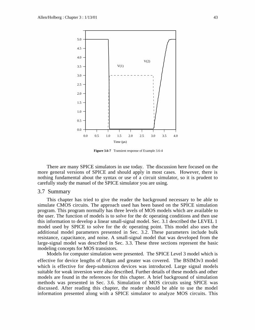
The last simulation to be made with Fig. 3.6-4 is the transient response to an inputpulse. This simulation will include the 5 pF output capacitor of the previous example andwill be made from time zero to 4 microseconds.

Allen/Holberg : Chapter 3 : 1/13/01 42
Table 3.6-4 shows the SPICE input file. The input pulse is described using thepiecewise linear capability (PWL) of SPICE. The output desired is defined by “.TRAN0.01U 4U” which asks for a transient analysis from 0 to 4 microseconds at pointsspaced every 0.01 microseconds. The output will consist of both vIN(t) and vOUT(t) and isshown in Fig. 3.6-7.
The above examples will serve to introduce the reader to the basic ideas andconcepts of using the SPICE program. In addition to what the reader has distilled fromthese examples, a useful set of guidelines is offered which has resulted from extensiveexperience in using SPICE. These guidelines are listed as:
1. Never use a simulator unless you know the range of answers beforehand.2. Never simulate more of the circuit than is necessary.3. Always use the simplest model that will do the job.4. Always start a dc solution from the point at which the majority of the devices are
on.5. Use a simulator in exactly the same manner as you would make the measurement
on the bench.6. Never change more than one parameter at a time when using the simulator for
design.7. Learn the basic operating principles of the simulator so that you can enhance its
capability. Know how to use its options.8. Watch out for syntax problems like O and 0.9. Use the correct multipliers for quantities.10. Use common sense.
Most problems with simulators can be traced back to a violation of one or more ofthese guidelines.
Table 3.6-4 SPICE Output for Example 3.6-4.Ex. 3.6-4 Transient Analysis of Fig. 3.6-3.M1 2 1 0 0 MOSN W=20U L=10UM2 2 3 4 4 MOSP W=10U L=20UM3 3 3 4 4 MOSP W=10U L=20UCL 2 0 5PR1 3 0 100KVDD 4 0 DC 5.0VIN 1 0 PWL(0 0V 1U 0V 1.05U 3V 3U 3V 3.05U 0V 6U 0V)*VIN 1 0 DC -2.42 AC 1.0.MODEL MOSN NMOS VTO=0.7 KP=110U GAMMA=0.4 LAMBDA=0.04 PHI=0.7.MODEL MOSP PMOS VTO=-0.7 KP=50U GAMMA=0.57 LAMBDA=0.05 PHI=0.8.TRAN 0.01U 4U.PRINT TRAN V(2) V(1).END
Allen/Holberg : Chapter 3 : 1/13/01 43
Figure 3.6-7 Transient response of Example 3.6-4
0.0 0.5 1.0 1.5 2.0 2.5 3.0 3.5 4.0
0.0
1.0
4.0
0.5
1.5
2.0
2.5
3.0
3.5
4.5
5.0
Time (µs)
V(1)
V(2)
There are many SPICE simulators in use today. The discussion here focused on themore general versions of SPICE and should apply in most cases. However, there isnothing fundamental about the syntax or use of a circuit simulator, so it is prudent tocarefully study the manuel of the SPICE simulator you are using.
3.7 SummaryThis chapter has tried to give the reader the background necessary to be able to
simulate CMOS circuits. The approach used has been based on the SPICE simulationprogram. This program normally has three levels of MOS models which are available tothe user. The function of models is to solve for the dc operating conditions and then usethis information to develop a linear small-signal model. Sec. 3.1 described the LEVEL 1model used by SPICE to solve for the dc operating point. This model also uses theadditional model parameters presented in Sec. 3.2. These parameters include bulkresistance, capacitance, and noise. A small-signal model that was developed from thelarge-signal model was described in Sec. 3.3. These three sections represent the basicmodeling concepts for MOS transistors.
Models for computer simulation were presented. The SPICE Level 3 model which iseffective for device lengths of 0.8µm and greater was covered. The BSIM3v3 modelwhich is effective for deep-submicron devices was introduced. Large signal modelssuitable for weak inversion were also described. Further details of these models and othermodels are found in the references for this chapter. A brief background of simulationmethods was presented in Sec. 3.6. Simulation of MOS circuits using SPICE wasdiscussed. After reading this chapter, the reader should be able to use the modelinformation presented along with a SPICE simulator to analyze MOS circuits. This

Allen/Holberg : Chapter 3 : 1/13/01 44
ability will be very important in the remainder of this text. It will be used to verifyintuitive design approaches and to perform analyses beyond the scope of the techniquespresented. One of the important aspects of modeling is to determine the model parameterswhich best fit the MOS process that is being used. The next chapter will be devoted tothis subject.

Allen/Holberg : Chapter 3 : 1/13/01 45
PROBLEMS1. Sketch to scale the output characteristics of an enhancement n-channel device if
VT = 0.7 volt and ID = 500 µA when VGS = 5 V in saturation. Choose values of VGS
= 1, 2, 3, 4, and 5 V. Assume that the channel modulation parameter is zero.2. Sketch to scale the output characteristics of an enhancement p-channel device if VT
= -0.7 volt and ID = -500 µA when VGS = -1, -2, -3, -4, and -6 V. Assume that thechannel modulation parameter is zero.
3. In Table 3.1-2, why is γP greater than γN for a n-well, CMOS technology?4. A large-signal model for the MOSFET which features symmetry for the drain and
source is given as
iD = K' WL [(vGS − VTS)2u(vGS − VTS)] − [(vGD − VTD)2u(vGD − VTD)]
where u(x) is 1 if x is greater than or equal to zero and 0 if x is less than zero (stepfunction) and VTX is the threshold voltage evaluated from the gate to X where X iseither S (Source) or D (Drain). Sketch this model in the form of iD versus vDS for aconstant value of vGS (vGS > VTS) and identify the saturated and nonsaturatedregions. Be sure to extend this sketch for both positive and negative values of vDS.Repeat the sketch of iD versus vDS for a constant value of vGD (vGD > VTD).Assume that both VTS and VTD are positive.
5. Equation (11) and Eq. (18) in Sec. 3.1 describe the MOS model in nonsaturationand saturation region, respectively. These equations do not agree at the point oftransition between between saturation and nonsaturation regions. For handcalculations, this is not an issue, but for computer analysis, it is. How would youchange Eq. (18) so that it would agree with Eq. (11) at vDS = vDS (sat)?
6. Using the values of Tables 3.1-1 and 3.2-1, calculate the values of CGB, CGS, andCGD for a MOS device which has a W of 5 µm and an L of 1 µm for all threeregions of operation
7. Find CBX at VBX = 0 V and 0.75 V of Fig. P3.7 assuming the values of Table 3.2-1
apply to the MOS device where FC = 0.5 and PB = 1 V. Assume the device is n-channel and repeat for a p-channel device.
1.6µm
Figure P3.7
2.0µm
Polysilicon
Metal
Active Area
0.8µm

Allen/Holberg : Chapter 3 : 1/13/01 46
8. Calculate the value of CGB, CGS, and CGD for an n-channel device with a length of1 µm and a width of 5 µm. Assume VD = 2 V, VG = 2.4 V, and VS = 0.5 V and let
VB = 0 V. Use model parameters from Tables 3.1-1, 3.1-2, and 3.2-1.9. Calculate the transfer function vout(s)/vin(s) for the circuit shown in Fig. P3.9. The
W/L of M1 is 2µm/0.8µm and the W/L of M2 is 4µm/4µm. Note that this is asmall-signal analysis and the input voltage has a dc value of 2 volts.
Figure P3.9
5 Volts
vIN = 2V(dc) + 1mV(rms)vout
+
-
W/L = 2/0.8
W/L = 4/4
10. Design a low-pass filter patterened after the circuit in Fig. P3.9 that achieves a -3dBfrequency of 100 KHz.
11. Repeat Examples 3.3-1 and 3.3-2 if the W/L ratio is 100 µm/10 µm.12. Find the complete small-signal model for an n-channel transistor with the drain at
4 V, gate at 4 V, source at 2 V, and the bulk at 0 V. Assume the model parameters
from Tables 3.1-1, 3.1-2, and 3.2-1, and W/L = 10 µm/1 µm.13. Consider the circuit in Fig P3.13. It is a parallel connection of n mosfet transistors.
Each transistor has the same length, L, but each transistor can have a differentwidth, W. Derive an expression for W and L for a single transistor that replaces, andis equivalent to, the multiple parallel transistors.
Figure P3.13
M1 M2 Mn
14. Consider the circuit in Fig P3.14. It is a series connection of n mosfet transistors.Each transistor has the same width, W, but each transistor can have a differentlength, L. Derive an expression for W and L for a single transistor that replaces, andis equivalent to, the multiple parallel transistors. When using the simple model, youmust ignore body effect.

Allen/Holberg : Chapter 3 : 1/13/01 47
Figure P3.14
M1
M2
Mn
15. Calculate the value for VON for n MOS transistor in weak inversion assuming thatfs and fn can be approximated to be unity (1.0).
16. Develop an expression for the small signal transconductance of a MOS deviceoperating in weak inversion using the large signal expression of Eq. (5) of Sec. 3.5.
17. Another way to approximate the transition from strong inversion to weak inversionis to find the current at which the weak-inversion transconductance and the strong-inversion transconductance are equal. Using this method and the approximation fordrain current in weak inversion (Eq. (5) of Sec. 3.5), derive an expression for draincurrent at the transition between strong and weak inversion.
18. Consider the circuit illustrated in Fig. P3.19. (a) Write a SPICE netlist thatdescribes this circuit. (b) Repeat part (a) with M2 being 2µm/1µm and it isintended that M3 and M2 are ratio matched, 1:2.
19. Use SPICE to perform the following analyses on the circuit shown in Fig. P3.19: (a)Plot vOUT versus vIN for the nominal parameter set shown. (b) Separately, vary K'and VT by +10% and repeat part (a)—four simulations.
Parameter N-Channel P-Channel UnitsVT 0.7 -0.7 VK' 110 50 µA/V2
l 0.04 0.05 V-1

Allen/Holberg : Chapter 3 : 1/13/01 48
vIN
vOUT
R =50kΩ1
2
3
4
Figure P3.19
VDD = 5 V
M1
M2M3
W/L = 1µ/1µ W/L = 1µ/1µ
W/L = 1µ/1µ
20. Use SPICE to plot i2 as a function of v2 when i1 has values of 10, 20, 30, 40, 50,60, and 70 µA for Fig. P3.20. The maximum value of v2 is 5 V. Use the model
parameters of VT = 0.7 V and K' = 110 µA/V2 and λ = 0.01 V-1. Repeat with λ =0.04 V-1.
v2
Figure P3.20
M1 M2
W/L = 10µm/2µm
i1 i2
W/L = 10µm/2µm
+
−
21. Use SPICE to plot iD as a function of vDS for values of vGS = 1, 2, 3, 4 and 5 V foran n-channel transistor with VT = 1 V, K' = 110 µA/V2, and l = 0.04 V-1. Showhow SPICE can be used to generate and plot these curves simultaneously asillustrated by Fig. 3.1-3.
22. Repeat Example 3.6-1 if the transistor of Fig. 3.6-5 is a PMOS having the modelparameters given in Table 3.1-2.
23. Repeat Examples 3.6-2 through 3.6-4 for the circuit of Fig. 3.6-2 if R1 = 200 KΩ.

Allen/Holberg : Chapter 3 : 1/13/01 49
REFERENCES1. Y. Tsividis, “Problems With Modeling of Analog MOS LSI,” IEDM, (1982) pp.
274-277.2. C.T. Sah, “Characteristics of the Metal-Oxide-Semiconductor Transistor,” IEEE
Transactions on Electron Devices, ED-11, No. 7(July 1964) pp. 324-345.3. H. Shichman and D. Hodges, “Modelling and Simulation of Insulated-Gate Field-
Effect Transistor Switching Circuits,” IEEE Journal Solid State Circuits, Vol. SC-3,No. 3 (September 1968) pp. 285-289.
4. A. Vladimirescu and S. Liu, “The Simulation of MOS Integrated Circuits usingSPICE2,” Memorandum No. UCB/ERL M80/7, October 1980, (ElectronicsResearch Laboratory, College of Engineering, University of California, Berkeley,CA 94720).
5. D.R. Alexander, R.J. Antinone, and G.W. Brown, “SPICE Modelling Handbook,”Report BDM/A-77-071-TR, (BDM Corporation, 2600 Yale Blvd., Albuquerque,NM 87106).
6. P.R. Gray and R.G. Meyer, “Analysis and Design of Analog Integrated Circuits,”Second Ed., (New York: John Wiley & Sons, 1984), p. 646.
7. P.E. Allen and E. Sanchez-Sinencio, “Switched Capacitor Circuits,” (New York:Van Nostrand Reinhold, 1984), p. 589.
8. R.D. Jolly and R.H. McCharles, “A Low-Noise Amplifier for Switched CapacitorFilters,” IEEE Journal of Solid-State Circuits, Vol. SC-17, No. 6, (December 1982),pp. 1192-1194.
9. Y.P. Tsividis, “Relation Between Incremental Intrinsic Capacitances andTransconductances in MOS Transistors,” IEEE Transactions on Electron Devices,Vol. ED-27, No. 5 (May 1980) pp. 946-948.
11. S. Liu and L.W. Nagel, “Small-Signal MOSFET Models for Analog CircuitDesign,” IEEE Journal of Solid-State Circuits, Vol. SC-17, No. 6 (December 1982)pp. 983-998.
12. F.H. Gaensslen and R.C. Jaeger, “Temperature Dependent Threshold Behavior ofDepletion Mode MOSFET’s,” Solid-State Electronics, Vol. 22, No. 4 (1979) pp.423-430.
13. D.E. Ward and R.W. Dutton, “A Charge-Oriented Model for MOS TransistorCapacitances,” IEEE Journal of Solid-State Circuits, Vol. SC-13, No. 5 (October1978).
14. R. Swanson and J.D. Meindl, “Ion-Implanted Complementary MOS Transistors inLow-Voltage Circuits,” IEEE Journal of Solid-State Circuits, Vol. SC-7, No. 2(April 1972) pp. 146-153.
15. Y. Tsividis, “Moderate Inversion In MOS Devices,” Solid State Electronics, Vol. 25,No. 11 (1982) pp. 1099-1104.
16. P. Antognetti, D.D. Caviglia, and E. Profumo, “CAD Model for Threshold andSubthreshold Conduction in MOSFET’s,” IEEE Journal of Solid-State Circuits, Vol.SC-17, No. 2 (June 1982) pp. 454-458.
17. E. Vittoz and J. Fellrath, “CMOS Analog Integrated Circuits Based on WeakInversion Operation,” IEEE Journal of Solid-State Circuits, Vol. SC-12, No. 3 (June1977) pp. 231-244.
18. M.G. DeGrauwe, J. Rigmenants, E. Vittoz, and H.J. DeMan, “Adaptive BiasingCMOS Amplifiers,” IEEE Journal of Solid-State Circuits, Vol. SC-17, No. 3 (June1982) pp. 522-528.

Allen/Holberg : Chapter 3 : 1/13/01 50
19. W. Steinhagen and W.L. Engl, “Design of Integrated Analog CMOS Circuits—AMultichannel Telemetry Transmitter,” IEEE Journal of Solid-State Circuits, Vol.SC-13, No. 6 (December 1978) pp. 799-805.
20. Y. Tsividis and R. Ulmer, “A CMOS voltage Reference,” IEEE Journal of Solid-State Circuits, Vol. SC-13, No. 6 (December 1978) pp. 774-778.
21. S.M. Sze, Physics of Semiconductor Devices, Second ed. (New York: John Wileyand Sons, 1981).
22. L.W. Nagel, SPICE2: A Computer Program to Simulate Semiconductor Circuits,ERL Memo No. ERL-M520, (Electronics Research Laboratory, University ofCalifornia, Berkeley, CA, May 1975).
23. A Vladimerescu, A.R. Newton, and D.O. Pederson, SPICE Version 2G.0 User’sGuide, September 1980 (University of California, Berkeley).
24. Silvaco International, SmartSpice Modeling Manual, September 1999, Volumes 1and 2.
25. Meta-Software, HSPICE User’s Manual, 199626. BSIM3v3 Manual (Final Version), Yuhua Cheng et al., Department of Electrical
Engineering and Computer Sciences, University of California, Berkeley, CA 947201995, 1996
27. J.R. Pierret, A MOS Parameter Extraction Program for the BSIM Model , ElectronicsResearch Laboratory, University of California, Berkeley, Calif., 94720.Memorandum No. UCB/ERL M84/99, November 21, 1984
28. Daniel P. Foty, MOSFET Modeling With SPICE: Principals and Practice, PrinticeHall Canada, 1997.
29. G. Massobrio and P. Antognetti, Semiconductor Device Modeling with SPICE, 2nded., McGraw-Hill, 1993.