wpt demonstrator - upcommons
TRANSCRIPT
Design and Implementation of a Controller for a Wireless
Power Transfer Demonstrator
A Degree Thesis
Submitted to the Faculty of the
Escola Tècnica Superior d'Enginyeria de
Telecomunicació de Barcelona
Universitat Politècnica de Catalunya
by
Daniel Perich Ibañez
In partial fulfilment
of the requirements for the degree in
TELECOMMUNICATIONS ENGINEERING
Advisors: Francesc Guinjoan Gispert
Kurt Schenk
Barcelona, June 2019

1
Abstract
This thesis describes the design and implementation of a controller for a wireless power
transfer (WPT) demonstrator. First, the system was simulated to examine the feasibility.
Then, an analog control was designed and tested as a previous step to the main goal of
the thesis: send data measurements wirelessly and use a PI controller to control the output
of the system to a constant value, independently of the position of the coils.
The controller is slower than expected due to a considerable delay in the data transmission,
but it manages to set the output voltage to a fixed value, which can be adjusted by a resistor,
for every position of the system.

2
Zusammenfassung
Diese Arbeit beschreibt das Design und die Implementierung einer Steuerung für einen
Wireless Power Transfer (WPT) Demonstrator. Zuerst wurde das System simuliert, um die
Machbarkeit zu prüfen. Danach wurde eine analoge Steuerung entworfen und getestet, als
ein vorheriger Schritt zum Hauptziel der Arbeit: Datenmessungen drahtlos senden und mit
einem PI-Regler den Ausgang des Systemsauf einen konstanten Wert steuern,
unabhängig von der Position der Spulen.
Die Steuerung ist aufgrund einer erheblichen Verzögerung der Datenübertragung
langsamer als erwartet. Es schafft aber, die Ausgangsspannung für jede Position des
Systems auf einen festen Wert einzustellen, der über einen Widerstand einstellbar ist.

3
Resum
Aquesta tesi descriu el disseny i la implementació d’un controlador per un demostrador de
transferència de potència sense fil. Primerament, el sistema va ser simulat per examinar
la viabilitat. Posteriorment, un control analògic va ser dissenyat i provat com pas previ a
l’objectiu principal de la tesi: enviar mesures de dades sense fil i utilitzar un controlador PI
per controlar el voltatge de sortida a un valor constant, independentment de la posició de
les bobines.
El controlador és més lent del previst degut a un retràs considerable a la transmissió de
dades, però aconsegueix fixar el voltatge de sortida a un valor fix, que pot ser ajustat amb
una resistència, per tota posició del sistema.

4
Resumen
Esta tesis describe el diseño y la implementación de un controlador para un demostrador
de transferencia inalámbrica de potencia. Primero, el sistema fue simulado para examinar
la viabilidad. Posteriormente, un control analógico fue diseñado y probado como paso
previo al objetivo principal de la tesis: enviar medidas de datos inalámbricamente y usar
un controlador PI para controlar el voltaje de salida a un valor constante,
independientemente de la posición de las bobinas.
El controlador es más lento de lo previsto debido a un retraso considerable en la
transmisión de datos, pero consigue fijar el voltaje de salida a un valor fijo, ajustable con
una resistencia, para toda posición del sistema.

5
To my family

6
Acknowledgements
First of all, I would like to thank my advisor Dr. Kurt Schenk for offering me the opportunity
to join the Power Electronics Laboratory at the NTB Buchs to work on the 3.5 kW
demonstrator. His help and support have been crucial to the development of this thesis,
thus his experience led to new ideas and solutions.
I would also like to thank Simon Nigsch for teaching me the functioning of the system and
providing a solution to every problem I have encountered and every doubt I have had. I
have learned a lot from him.
Another thanks belongs to the staff at the laboratory, who have always been eager to help
me in any way they could, in particular Falk Kyburz and Stefan Klammer.
Last, but not least, I thank my advisor in my university, Dr. Francesc Guinjoan, for his advice
at the beginning of the thesis and for his time reviewing it.

7
Revision history and approval record
Revision Date Purpose
0 04/03/2019 Document creation
1 18/04/2019 Document revision
2 08/05/2019 Document revision 1
3 21/05/2019 Document revision 2
4 03/06/2019 Document revision 3
5 14/06/2019 Document revision 4
6 21/06/2019 Final Revision
DOCUMENT DISTRIBUTION LIST
Name e-mail
Daniel Perich Ibañez [email protected]
Kurt Schenk [email protected]
Francesc Guinjoan Gispert [email protected]
Written by: Reviewed and approved by:
Date 21/06/2019 Date 21/06/2019
Name Daniel Perich Ibañez Name Kurt Schenk
Position Project Author Position Project Supervisor

8
Table of contents
Abstract ............................................................................................................................................. 1
Zusammenfassung ............................................................................................................................ 2
Resum ............................................................................................................................................... 3
Resumen ........................................................................................................................................... 4
Acknowledgements ........................................................................................................................... 6
Revision history and approval record ................................................................................................ 7
Table of contents ............................................................................................................................... 8
List of Figures .................................................................................................................................... 9
List of Tables ................................................................................................................................... 10
1. Introduction .............................................................................................................................. 11
2. State of the art of the technology used or applied in this thesis .............................................. 15
3. Methodology / project development ........................................................................................ 16
3.1. Simulation ........................................................................................................................ 16
3.2. PCB Design for Analog Control ....................................................................................... 21
3.3. Microcontroller ................................................................................................................. 24
3.3.1. Receiver side ........................................................................................................... 25
3.3.2. Transmitter side ....................................................................................................... 28
3.3.3. Code ........................................................................................................................ 30
4. Results ..................................................................................................................................... 34
4.1. Simulation ........................................................................................................................ 34
4.2. PCB Design for Analog Control ....................................................................................... 38
4.3. Microcontroller ................................................................................................................. 39
5. Budget ..................................................................................................................................... 45
5.1. Analog Control ................................................................................................................. 45
5.2. Microcontroller PCBs ....................................................................................................... 46
6. Conclusions and future development ...................................................................................... 48
Bibliography ..................................................................................................................................... 49
Appendices ...................................................................................................................................... 50
1. Provided schematics ............................................................................................................... 50
2. Analog design .......................................................................................................................... 52
3. Receiver side ........................................................................................................................... 54
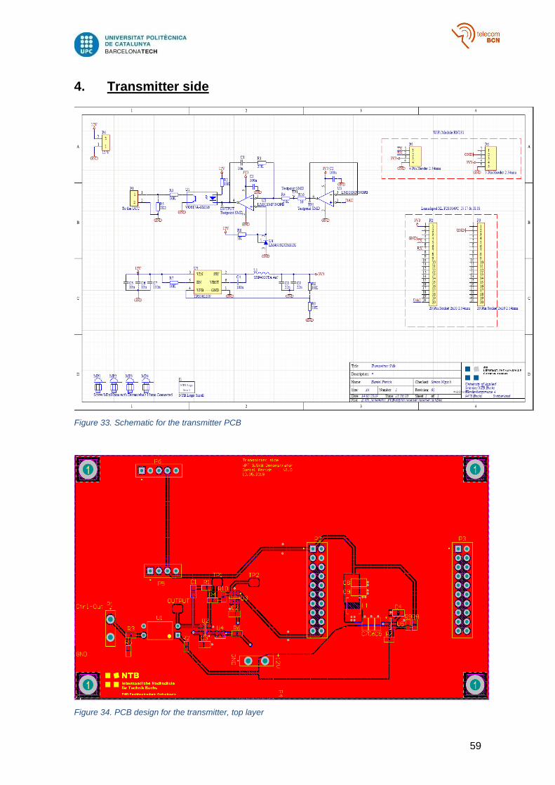
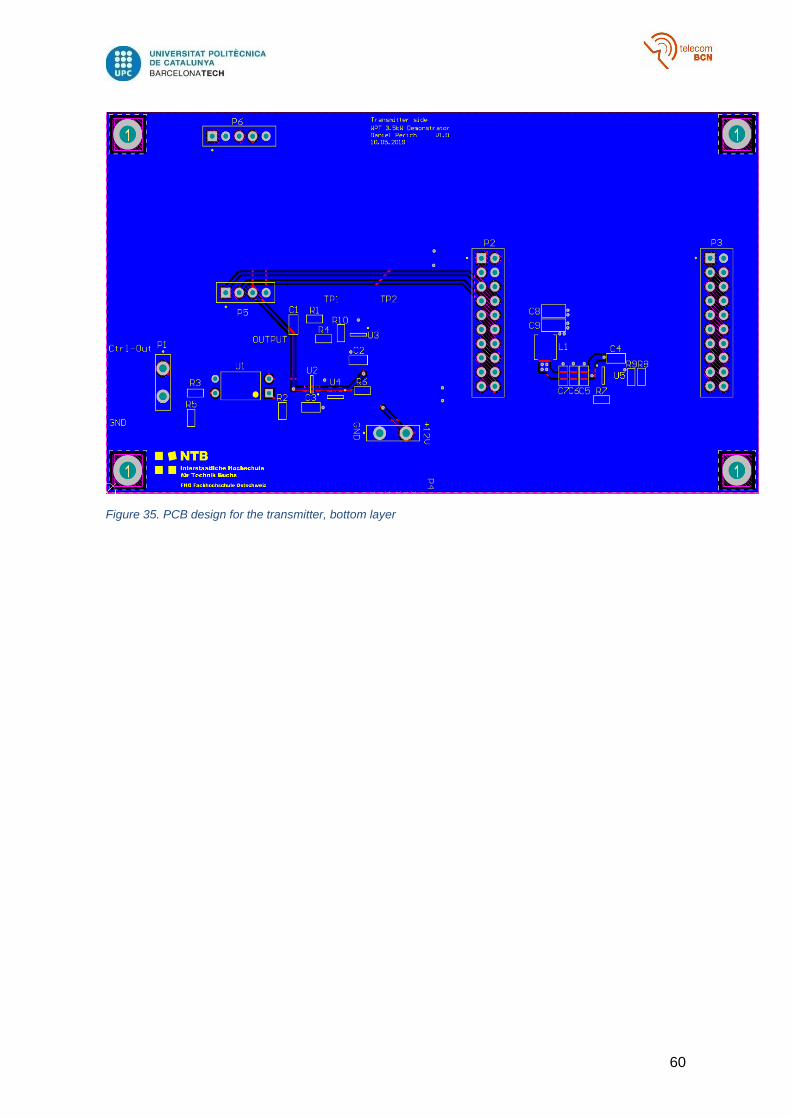
4. Transmitter side ....................................................................................................................... 59
5. Loop gain measurements ........................................................................................................ 65
Glossary .......................................................................................................................................... 71
9
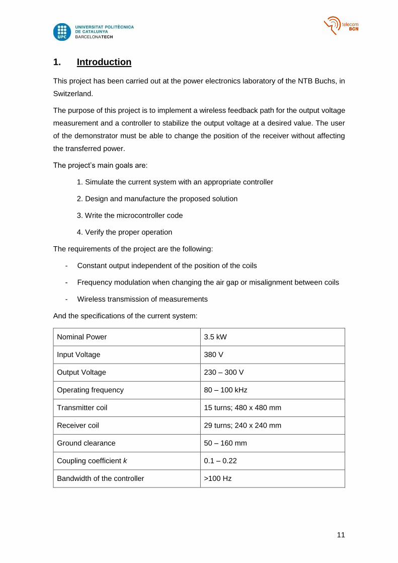
List of Figures
Figure 1. Gantt Diagram .................................................................................................................. 14
Figure 2. Simulation model of the current demonstrator ................................................................. 16
Figure 3. Capacitor configuration for the secondary side................................................................ 17
Figure 4. Analog controller simulation model .................................................................................. 18
Figure 5. Simulation model for the analog controller with Op Amp ................................................. 19
Figure 6. Altium schematic for the analog control ........................................................................... 21
Figure 7. PCB design for the analog control ................................................................................... 23
Figure 8. Wi-Fi Module .................................................................................................................... 24
Figure 9. Receiver side schematic .................................................................................................. 25
Figure 10. PCB design for the receiver ........................................................................................... 27
Figure 11. Transmitter side schematic ............................................................................................ 28
Figure 12. PCB design for the transmitter ....................................................................................... 29
Figure 13. Output voltage and current of the demonstrator ............................................................ 34
Figure 14. Primary and secondary currents .................................................................................... 34
Figure 15. Output voltage, current and PI with analog control ........................................................ 35
Figure 16. Primary and secondary currents for the analog control ................................................. 36
Figure 17. Output voltage, current and controller with Op Amp ...................................................... 36
Figure 18. Primary and Secondary currents for Op Amp control .................................................... 37
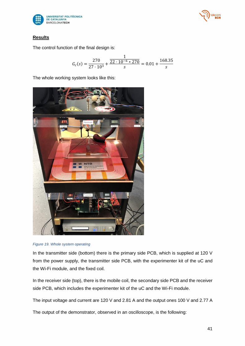
Figure 19. Whole system operating ................................................................................................. 41
Figure 20. System output when moving the coil ............................................................................. 42
Figure 21. Bode plot of the controller .............................................................................................. 42
Figure 22. Bode plot of the system with modified parameters ........................................................ 43
Figure 23. Final bode plot of the system ......................................................................................... 44
Figure 24. Output of the optimized system ..................................................................................... 44
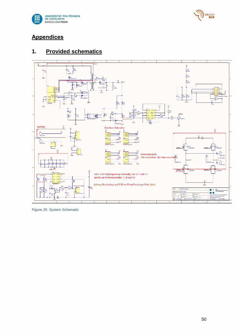
Figure 25. System Schematic ......................................................................................................... 50
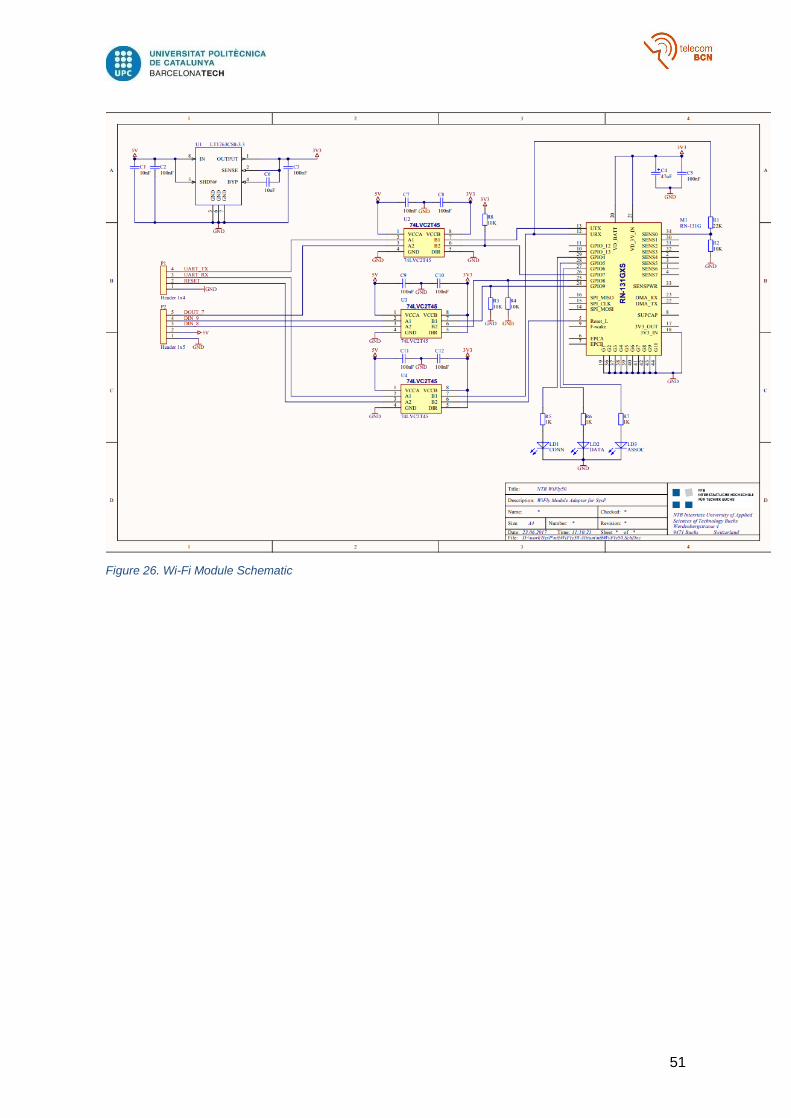
Figure 26. Wi-Fi Module Schematic ................................................................................................ 51
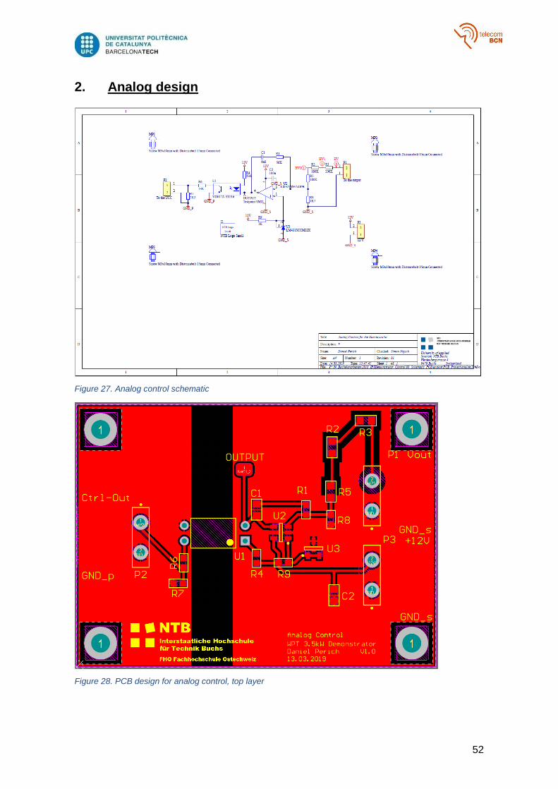
Figure 27. Analog control schematic ............................................................................................... 52
Figure 28. PCB design for analog control, top layer ....................................................................... 52
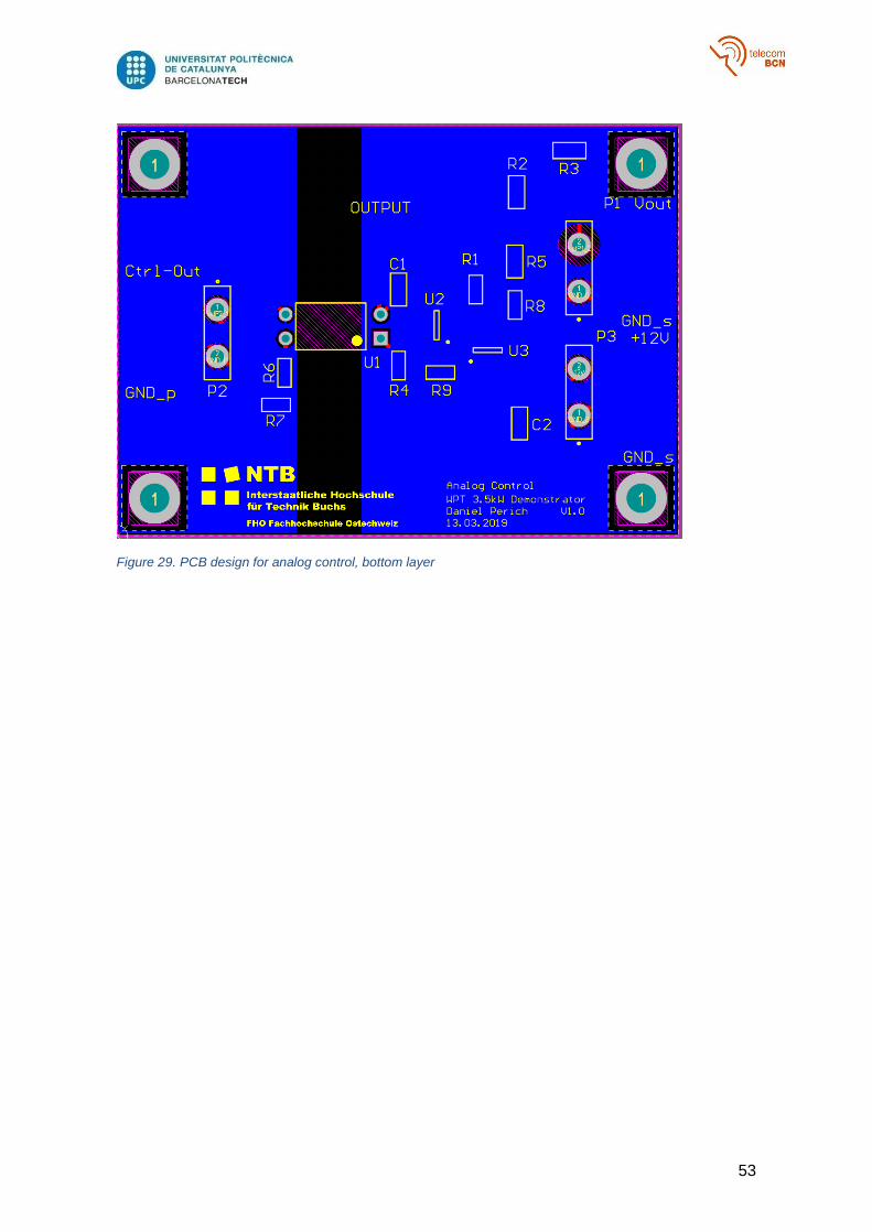
Figure 29. PCB design for analog control, bottom layer ................................................................. 53
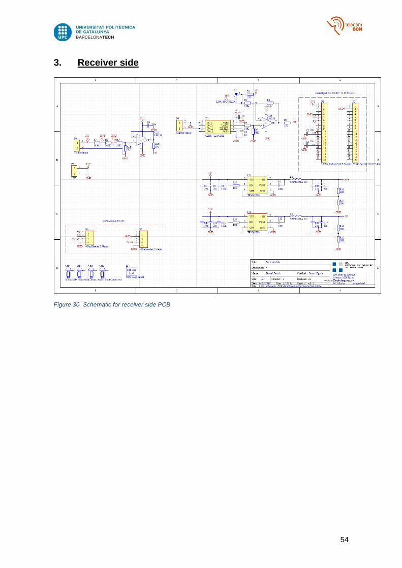
Figure 30. Schematic for receiver side PCB ................................................................................... 54
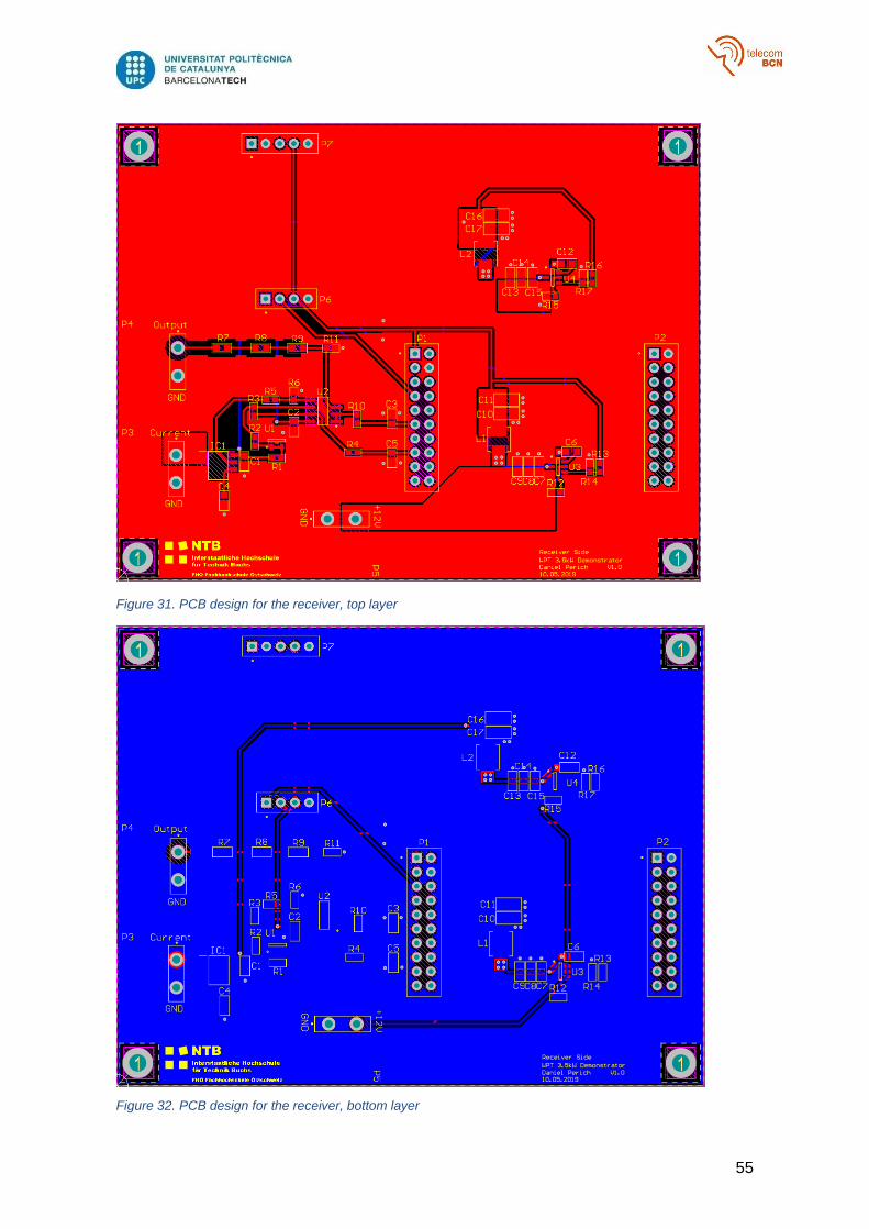
Figure 31. PCB design for the receiver, top layer ........................................................................... 55
Figure 32. PCB design for the receiver, bottom layer ..................................................................... 55
Figure 33. Schematic for the transmitter PCB ................................................................................. 59
Figure 34. PCB design for the transmitter, top layer ....................................................................... 59
Figure 35. PCB design for the transmitter, bottom layer ................................................................. 60

10
List of Tables
Table 1. Parameters for the leakage and magnetizing inductances ............................................... 17
Table 2. Optimum switching frequency for every position of the demonstrator .............................. 35
Table 3. Current readings and voltage measurements without calibration ..................................... 40
Table 4. Current readings with calibration ....................................................................................... 40
Table 5. Component list for the analog control PCB ....................................................................... 45
Table 6. Component list for the microcontroller PCBs .................................................................... 46
11
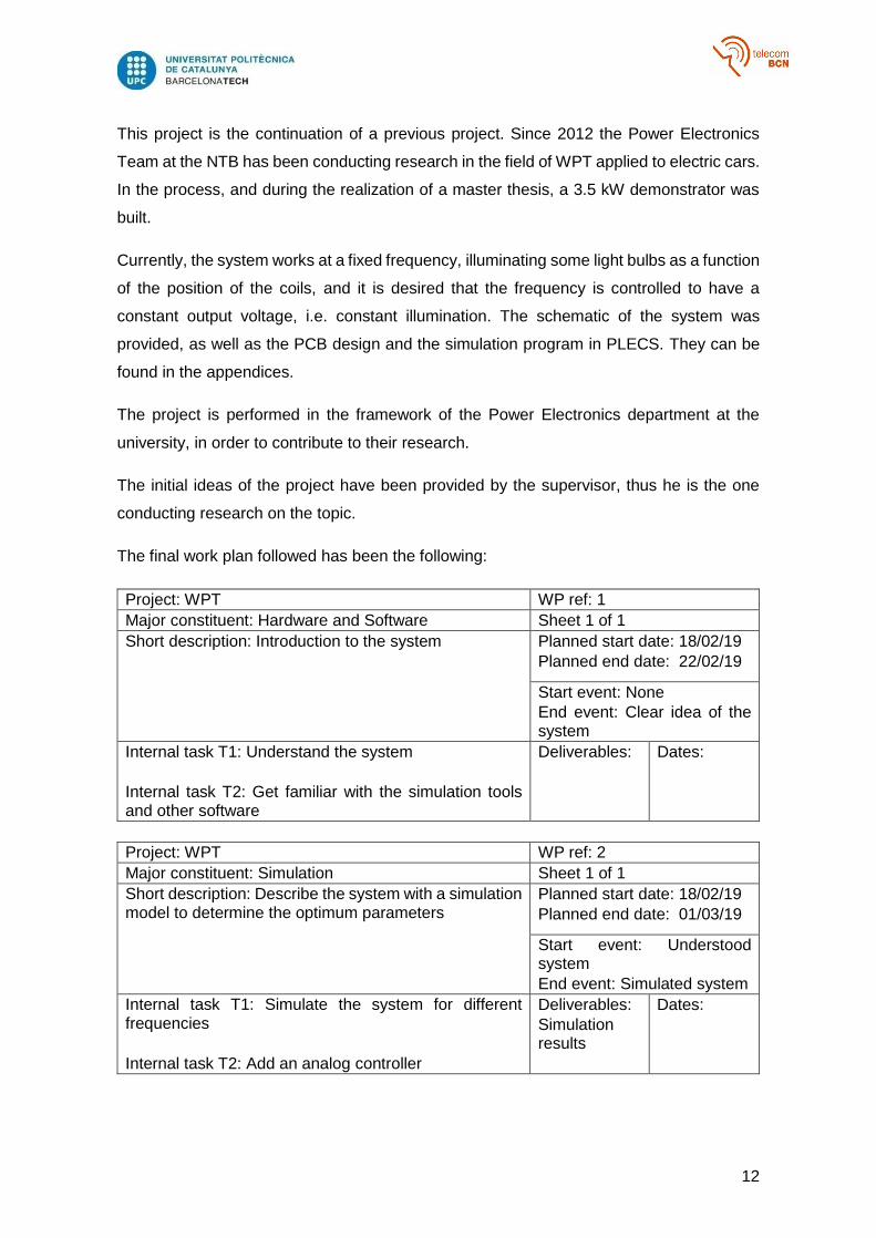
1. Introduction
This project has been carried out at the power electronics laboratory of the NTB Buchs, in
Switzerland.
The purpose of this project is to implement a wireless feedback path for the output voltage
measurement and a controller to stabilize the output voltage at a desired value. The user
of the demonstrator must be able to change the position of the receiver without affecting
the transferred power.
The project’s main goals are:
1. Simulate the current system with an appropriate controller
2. Design and manufacture the proposed solution
3. Write the microcontroller code
4. Verify the proper operation
The requirements of the project are the following:
- Constant output independent of the position of the coils
- Frequency modulation when changing the air gap or misalignment between coils
- Wireless transmission of measurements
And the specifications of the current system:
Nominal Power 3.5 kW
Input Voltage 380 V
Output Voltage 230 – 300 V
Operating frequency 80 – 100 kHz
Transmitter coil 15 turns; 480 x 480 mm
Receiver coil 29 turns; 240 x 240 mm
Ground clearance 50 – 160 mm
Coupling coefficient k 0.1 – 0.22
Bandwidth of the controller >100 Hz
12
This project is the continuation of a previous project. Since 2012 the Power Electronics
Team at the NTB has been conducting research in the field of WPT applied to electric cars.
In the process, and during the realization of a master thesis, a 3.5 kW demonstrator was
built.
Currently, the system works at a fixed frequency, illuminating some light bulbs as a function
of the position of the coils, and it is desired that the frequency is controlled to have a
constant output voltage, i.e. constant illumination. The schematic of the system was
provided, as well as the PCB design and the simulation program in PLECS. They can be
found in the appendices.
The project is performed in the framework of the Power Electronics department at the
university, in order to contribute to their research.
The initial ideas of the project have been provided by the supervisor, thus he is the one
conducting research on the topic.
The final work plan followed has been the following:
Project: WPT WP ref: 1
Major constituent: Hardware and Software Sheet 1 of 1
Short description: Introduction to the system
Planned start date: 18/02/19
Planned end date: 22/02/19
Start event: None
End event: Clear idea of the system
Internal task T1: Understand the system
Internal task T2: Get familiar with the simulation tools and other software
Deliverables: Dates:
Project: WPT WP ref: 2
Major constituent: Simulation Sheet 1 of 1
Short description: Describe the system with a simulation model to determine the optimum parameters
Planned start date: 18/02/19
Planned end date: 01/03/19
Start event: Understood system
End event: Simulated system
Internal task T1: Simulate the system for different frequencies
Internal task T2: Add an analog controller
Deliverables:
Simulation results
Dates:
13
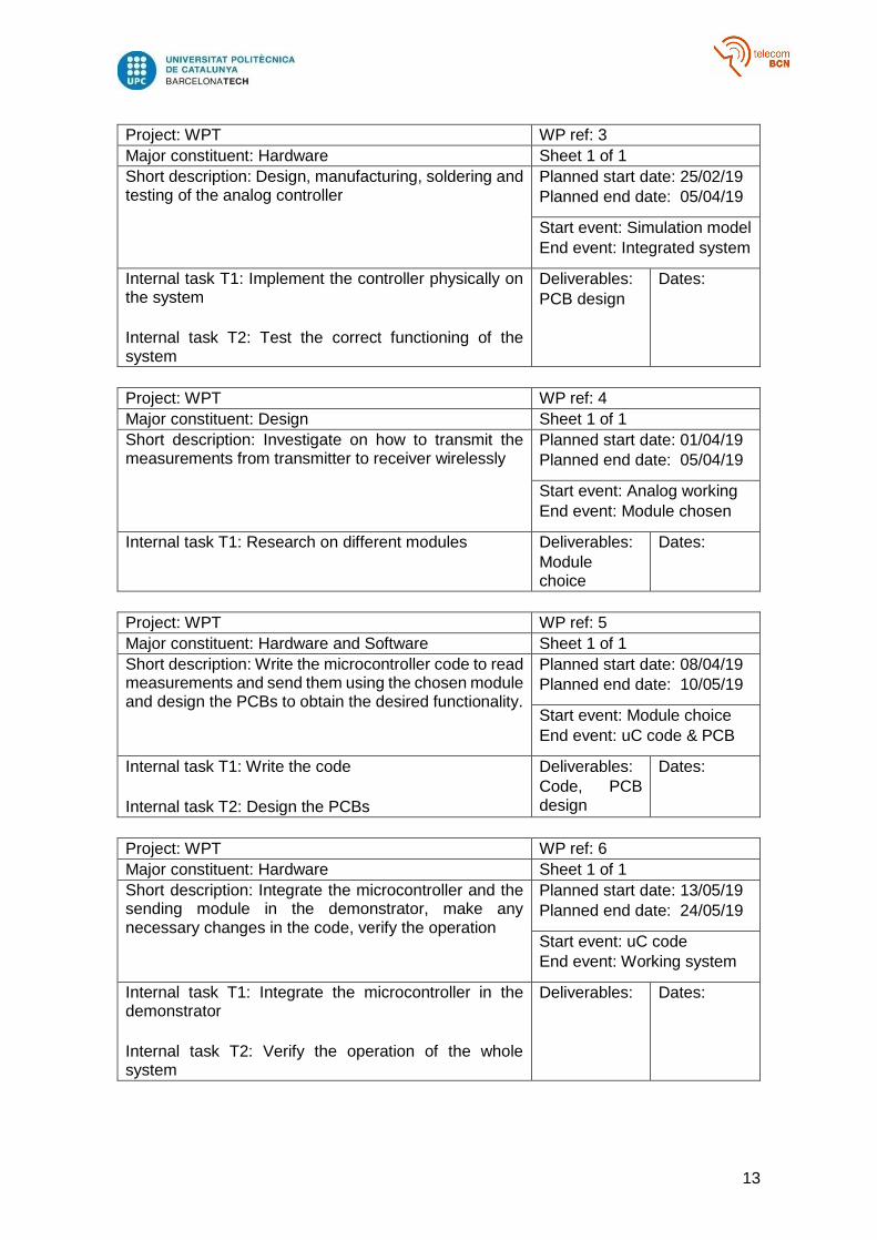
Project: WPT WP ref: 3
Major constituent: Hardware Sheet 1 of 1
Short description: Design, manufacturing, soldering and testing of the analog controller
Planned start date: 25/02/19
Planned end date: 05/04/19
Start event: Simulation model
End event: Integrated system
Internal task T1: Implement the controller physically on the system
Internal task T2: Test the correct functioning of the system
Deliverables:
PCB design
Dates:
Project: WPT WP ref: 4
Major constituent: Design Sheet 1 of 1
Short description: Investigate on how to transmit the measurements from transmitter to receiver wirelessly
Planned start date: 01/04/19
Planned end date: 05/04/19
Start event: Analog working
End event: Module chosen
Internal task T1: Research on different modules Deliverables:
Module choice
Dates:
Project: WPT WP ref: 5
Major constituent: Hardware and Software Sheet 1 of 1
Short description: Write the microcontroller code to read measurements and send them using the chosen module and design the PCBs to obtain the desired functionality.
Planned start date: 08/04/19
Planned end date: 10/05/19
Start event: Module choice
End event: uC code & PCB
Internal task T1: Write the code
Internal task T2: Design the PCBs
Deliverables:
Code, PCB design
Dates:
Project: WPT WP ref: 6
Major constituent: Hardware Sheet 1 of 1
Short description: Integrate the microcontroller and the sending module in the demonstrator, make any necessary changes in the code, verify the operation
Planned start date: 13/05/19
Planned end date: 24/05/19
Start event: uC code
End event: Working system
Internal task T1: Integrate the microcontroller in the demonstrator
Internal task T2: Verify the operation of the whole system
Deliverables:
Dates:

14
Project: WPT WP ref: 7
Major constituent: Measurements Sheet 1 of 1
Short description: Measure the behavior of the controller using a loop gain analyzer, determine whether it is stable enough, try to optimize it
Planned start date: 27/05/19
Planned end date: 07/06/19
Start event: Working system
End event: Measurements
Internal task T1: Measure the behavior of the controller
Internal task T2: Try to optimize it
Deliverables:
Measurements
Dates:
Milestones
WP# Task# Short title Milestone / deliverable Date (week)
2 2 Analog simulation Simulation results 9
3 1 PCB PCB Design 14
4 1 Design Module choice 14
5 1 Firmware uC Code 19
5 2 PCB PCB Designs 19
7 1&2 Final test Measurements results 23
And the gantt diagram:
Initially, the idea was to implement a digital controller for the system but, since the analog
part took longer than expected because it was not working appropriately, the thesis was
rethought. No other major deviations happened.
Tasks \ Week 8 9 10 11 12 13 14 15 16 17 18 19 20 21 22 23
Understand the system
Get familiar with the software
Simulation with analog controller
Implementation and testing
Choice of transmission module
Microcontroller code
System integration
Measurements and optimization
Writing the thesis
Figure 1. Gantt Diagram

15
2. State of the art of the technology used or applied in this
thesis
The main technology applied in this thesis is control theory, in particular PI controllers.
A PI (Proportional-Integral) Controller calculates an error value as the difference between
a reference and a measured variable and corrects it based on proportional and integral
coefficients.
The output power equals the sum of proportional and integration coefficients.
The control function can be expressed as:
𝐺𝑐(𝑠) = 𝐾𝑝 (𝑠 +
1𝑇𝑖
𝑠) = 𝐾𝑝 +
𝐾𝑖
𝑠
Where 𝐾𝑝 is the proportional term and 𝐾𝑖 the integral one.
If 𝐾𝑝 is too high, the system can become unstable since there will be a large variation in
the output for a certain change in the error. On the contrary, if it is too low, the control action
may be too small and unable to control the system.
The larger the proportional coefficient, the smaller the steady state error.
The integral term takes into account the magnitude of the error and its duration. It
accumulates the instantaneous error over time, giving the offset which should have been
corrected previously, and is added to the controller output multiplied by the integral gain 𝐾𝑖.
In order to eliminate the steady state error, the PI adds a zero at 𝑠 = −1
𝑇𝑖 and a pole at s =
0 (origin), yielding the control function above.
16
3. Methodology / project development
3.1. Simulation
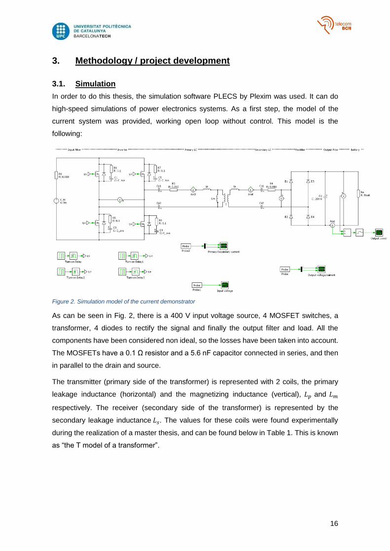
In order to do this thesis, the simulation software PLECS by Plexim was used. It can do
high-speed simulations of power electronics systems. As a first step, the model of the
current system was provided, working open loop without control. This model is the
following:
Figure 2. Simulation model of the current demonstrator
As can be seen in Fig. 2, there is a 400 V input voltage source, 4 MOSFET switches, a
transformer, 4 diodes to rectify the signal and finally the output filter and load. All the
components have been considered non ideal, so the losses have been taken into account.
The MOSFETs have a 0.1 Ω resistor and a 5.6 nF capacitor connected in series, and then
in parallel to the drain and source.
The transmitter (primary side of the transformer) is represented with 2 coils, the primary
leakage inductance (horizontal) and the magnetizing inductance (vertical), 𝐿𝑝 and 𝐿𝑚
respectively. The receiver (secondary side of the transformer) is represented by the
secondary leakage inductance 𝐿𝑠. The values for these coils were found experimentally
during the realization of a master thesis, and can be found below in Table 1. This is known
as “the T model of a transformer”.

17
Table 1. Parameters for the leakage and magnetizing inductances
Air gap [mm] 50 105 160
Misalignment
[mm]
0 50 100 0 50 100 0 50 100
𝐿𝑝 [µH] 266.9 267.2 273.6 278.3 279.5 283.7 286.5 287.3. 288.1
𝐿𝑚 [µH] 41.2 41.9 41.6 28.9 28.3 25.9 20.1 19.5 17.3
𝐿𝑠 [µH] 274.2 270.6 271.6 277.8 279.8 288.6 305.4 307.7 316.3
Moreover, capacitors are added to compensate the leakage inductance losses, both in the
primary and secondary side, as well as 10 mΩ resistors. The values for the capacitors can
be found by observation of the current system. For the primary side capacitor, there are
two blocks of 6 capacitors connected in series, and then 12 times in parallel. Both blocks
are connected in series. Each capacitor has a value of 10 nF, so the total capacitance
is 10 nF ∗12
6∗
1
2= 10 nF.
For the secondary side, there are two blocks of 3 capacitors connected in series, and then
8 times in parallel. Both blocks are connected in series. Each capacitor has a value of 5.6
nF, so the total capacitance is 5.6 nF ∗8
3∗
1
2= 7.47 nF. The configuration is as follows:
Figure 3. Capacitor configuration for the secondary side
For simplicity, the configuration is only represented for the secondary side, but the primary
one is analogous.
18
For the simulation, both 𝐶𝑝 and 𝐶𝑠 have been represented by 2 capacitors in series, with
values 2 · 𝐶𝑝 and 2 · 𝐶𝑠 respectively.
The transformer used in the simulation is an ideal one, with 15 turns in the primary side
and 29 in the secondary, as it is in the demonstrator.
The 4 rectifying diodes have been set to have an on resistance of 10 mΩ, the capacitor 𝐶0
has a capacitance of 20 µF and the load 𝑅0 can be found using 𝑅0 =𝑉𝑜𝑢𝑡
2
𝑃𝑜𝑢𝑡 . In the current
system, the output voltage is expected to be 300 V and the output power 3000 W, so the
output load is 𝑅0 =3002
3000= 30 Ω.
The MOSFETs’ switching frequency is controlled by applying pulses of a certain frequency
to their gates. Q1 and Q4 are activated simultaneously and Q2 and Q3 as well, with a
phase delay of 1
2𝑓. The pulses have an amplitude of 1 V and duty cycle of 50 %, and the
frequency is set by the user. The nominal frequency is 97 kHz, but it varies according to
the air gap or misalignment between the coils. Finally, there is a dead time of 200 ns, which
is the turn on delay.
The results of this simulation will be presented in the next chapter.
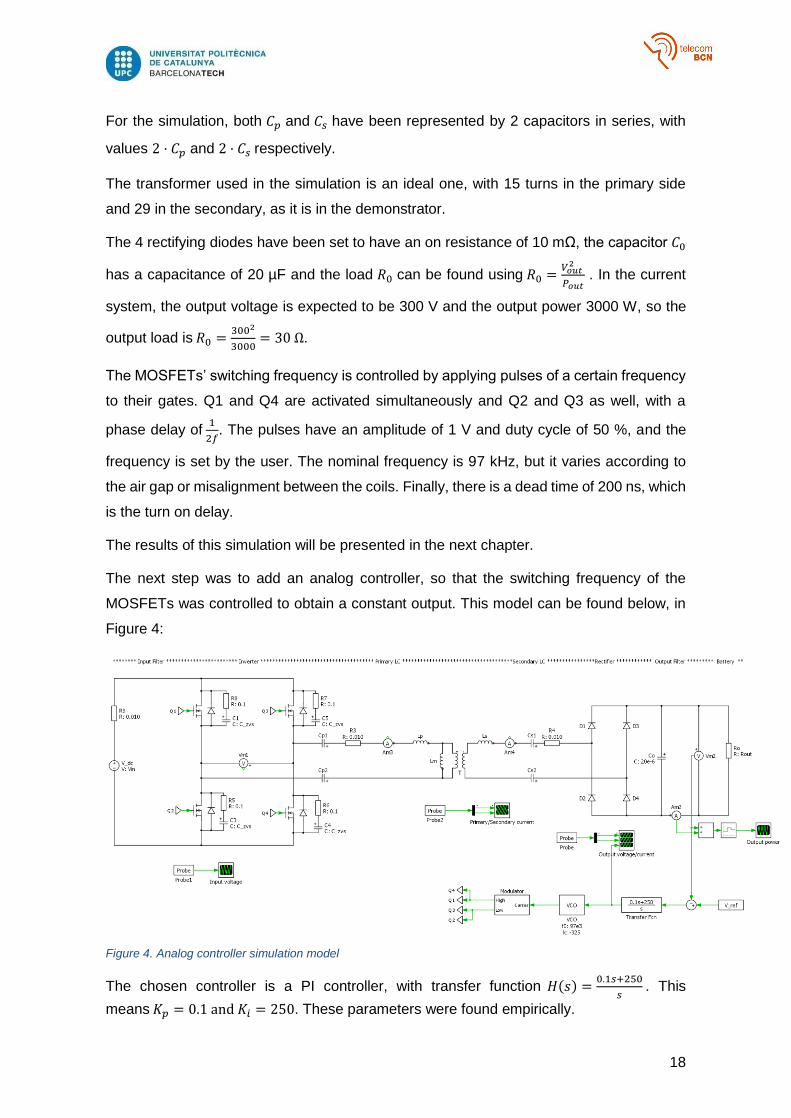
The next step was to add an analog controller, so that the switching frequency of the
MOSFETs was controlled to obtain a constant output. This model can be found below, in
Figure 4:
Figure 4. Analog controller simulation model
The chosen controller is a PI controller, with transfer function 𝐻(𝑠) =0.1𝑠+250
𝑠. This
means 𝐾𝑝 = 0.1 and 𝐾𝑖 = 250. These parameters were found empirically.
19
The error of the controller is calculated by subtracting a voltage reference, which is the 300
V desired output, and the output voltage of the demonstrator. At the output of the PI
controller, a VCO is connected. The VCO model was provided by the Power Electronics
team. The quiescent frequency is 97 kHz and the gain is –325.
This parameter has also been found by trial and error. Finally, the output of the VCO, a
sinusoidal signal with frequency proportional to the input signal, is connected to a
modulator, which creates alternating pulses to drive the transistors, as done in the first
approach with pulses.
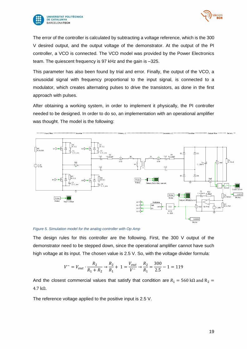
After obtaining a working system, in order to implement it physically, the PI controller
needed to be designed. In order to do so, an implementation with an operational amplifier
was thought. The model is the following:
Figure 5. Simulation model for the analog controller with Op Amp
The design rules for this controller are the following. First, the 300 V output of the
demonstrator need to be stepped down, since the operational amplifier cannot have such
high voltage at its input. The chosen value is 2.5 V. So, with the voltage divider formula:
𝑉− = 𝑉𝑜𝑢𝑡 ·𝑅2
𝑅1 + 𝑅2→
𝑅2
𝑅1+ 1 =
𝑉𝑜𝑢𝑡
𝑉−→
𝑅2
𝑅1=
300
2.5− 1 = 119
And the closest commercial values that satisfy that condition are 𝑅1 = 560 kΩ and R2 =
4.7 kΩ.
The reference voltage applied to the positive input is 2.5 V.

20
In order to obtain the transfer function of the amplifier, the circuit was analyzed using
Kirchhoff’s laws. The obtained transfer function is:
𝐻(𝑠) =𝑉𝑜𝑢𝑡
𝑉𝑖𝑛= − (
𝑅10
𝑅1+
1𝑅1𝐶2
𝑠)
Comparing it with the obtained PI controller 𝐻(𝑠) = 0.1 +250
𝑠, it is easy to see that
𝑅10
𝑅1= 0.1 and
1
𝑅1𝐶2= 250 . Since 𝑅1 is already fixed by the voltage divider, the other
parameters are:
𝐾𝑝 =𝑅10
𝑅1→ 𝑅10 = 𝑅1 · 𝐾𝑝 = 56 kΩ 𝐾𝑖 =
1
𝑅1𝐶2→ 𝐶2 =
1
𝑅1𝐾𝑖= 7,14 nF
The resistor value is already a commercial value, since it is only a factor of 10 of the
chosen for the voltage divider, but the capacitor is not. Therefore, the chosen value for 𝐶2
is 6.8 nF.
21
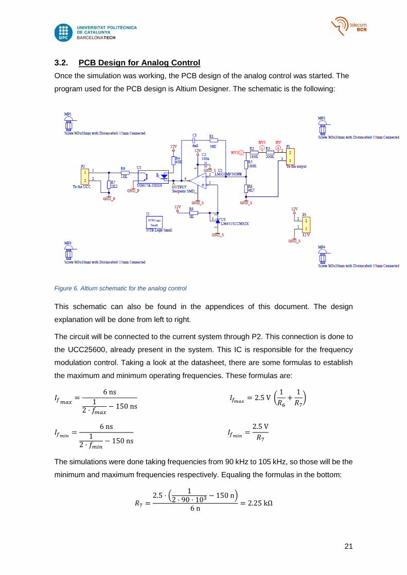
3.2. PCB Design for Analog Control
Once the simulation was working, the PCB design of the analog control was started. The
program used for the PCB design is Altium Designer. The schematic is the following:
Figure 6. Altium schematic for the analog control
This schematic can also be found in the appendices of this document. The design
explanation will be done from left to right.
The circuit will be connected to the current system through P2. This connection is done to
the UCC25600, already present in the system. This IC is responsible for the frequency
modulation control. Taking a look at the datasheet, there are some formulas to establish
the maximum and minimum operating frequencies. These formulas are:
𝐼𝑓𝑚𝑎𝑥=
6 ns
12 · 𝑓𝑚𝑎𝑥
− 150 ns 𝐼𝑓𝑚𝑎𝑥
= 2.5 V (1
𝑅6+
1
𝑅7)
𝐼𝑓𝑚𝑖𝑛=
6 ns
12 · 𝑓𝑚𝑖𝑛
− 150 ns 𝐼𝑓𝑚𝑖𝑛
=2.5 V
𝑅7
The simulations were done taking frequencies from 90 kHz to 105 kHz, so those will be the
minimum and maximum frequencies respectively. Equaling the formulas in the bottom:
𝑅7 =2.5 · (
12 · 90 · 103 − 150 n)
6 n= 2.25 kΩ
22
And, for 𝑅6,
𝐼𝑓𝑚𝑎𝑥=
6 n
12 · 105 · 103 − 150 n
= 1.3 mA
1.3 · 10−3 = 2.5 · (1
𝑅6+
1
2.25 · 103) →
1
𝑅6=
1.3 · 10−3
2.5−
1
2.25 · 103= 75.56 · 10−6 →
𝑅6 =1
75.56 · 10−6= 13,235 kΩ
Taking the closest available components, the chosen values for 𝑅6 and 𝑅7 are,
respectively, 13 kΩ and 2.2 kΩ.
The next component is the VO617a. This is an optocoupler, which provides galvanic
isolation between the primary and secondary side and transmits the output of the controller.
The infrared diode emitter needs to be powered to work, so it is connected to the 12 V from
an auxiliary power supply source through a 43 kΩ resistor, to generate some current.
Furthermore, the Op Amp LM321 was used, with the parameters calculated in the
simulation. It is powered with 12 V and needs a 100 nF capacitor between Vcc and GND
to decouple. In order to obtain the 2.5 V reference voltage at the inverting input, the LM431
is used. It is an adjustable Zener shunt regulator, which has a reference of 2.5 V when
powered with at least 1 mA and up to 100 mA. Therefore, the IC is powered with 12 V
through a 1 kΩ resistor, thus 𝐼 =𝑉𝑖𝑛−𝑉𝑜𝑢𝑡
𝑅=
12−2.5
1 k= 9.5 mA
At the inverting input of the Op Amp, the stepped-down output of the demonstrator is
connected, with the previously calculated parameters.
It is worth noticing that the 560 kΩ resistor in the voltage divider has been split in 3 series
resistors. This is because the output of the demonstrator is expected to be 300 V, and just
one resistor would not be able to work properly.
The power loss would be: 𝑃 =𝑉2
𝑅=
3002
560·103 = 160,71 mW
And SMD resistors used are designed for 100 mW only, if cooled appropriately. To avoid
any future problems, a 200 kΩ and two 180 kΩ resistors are used.
Also, the ground in the primary side is different than the one in the secondary. This is
because both sides should not be connected, since there needs to be isolation.
23
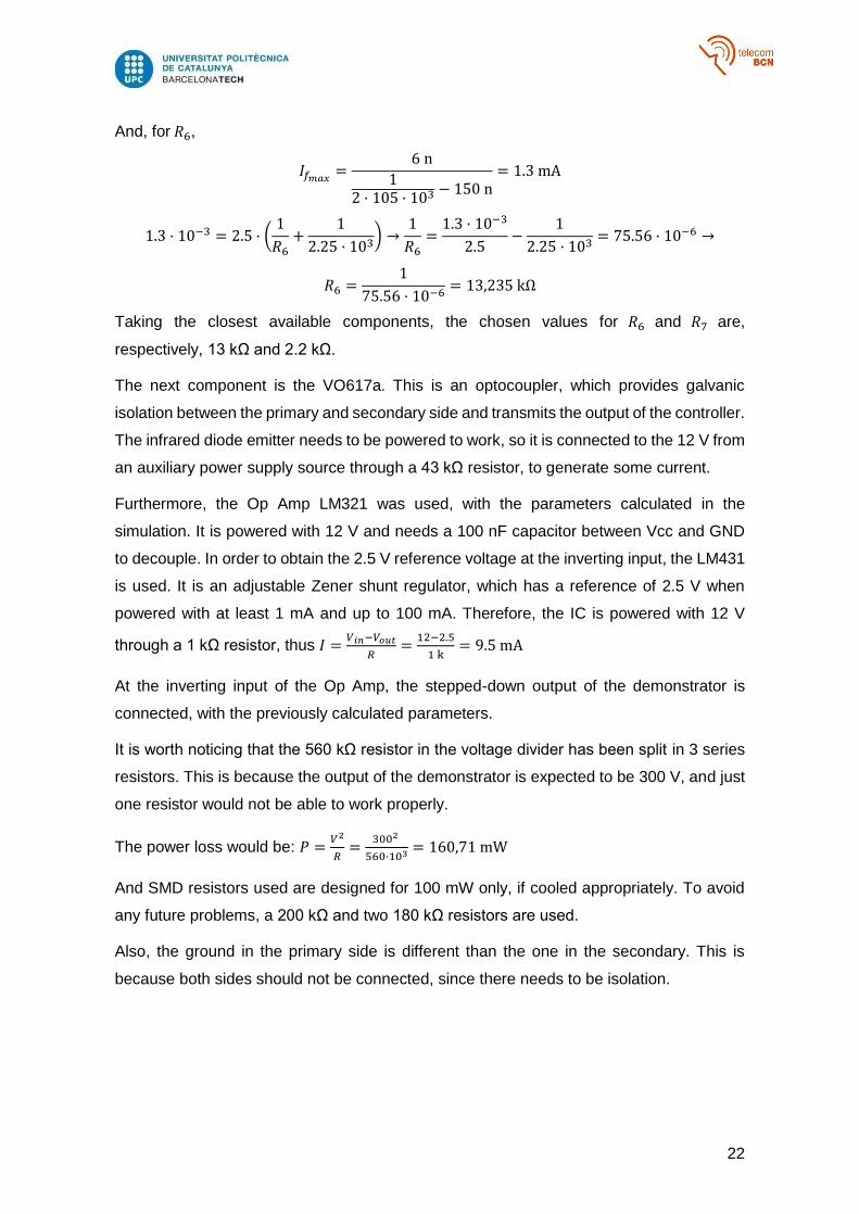
All in all, the PCB design looks like this:
Figure 7. PCB design for the analog control
It is worth pointing out that the tracks from P1 and R3 on the right, as well as from R3 to
R2 and R2 to R5, have a wider clearance to GND than the rest. This is because a high
voltage will flow through those tracks and the clearance needs to be increased. Also, all
resistors are 0603 while the ones with high voltage are 0805.
24
3.3. Microcontroller
The next step was to send the output voltage and current measurements to the primary
side.
In order to do so, an experimenter kit C2000 Launchpad XL was used, based on the
microcontroller TMS320F28027 from Texas Instruments. The measurements were
obtained using the ADC pins. This particular microcontroller works at 3.3 V, and 4096
samples. Therefore, the formula used to convert the reading to voltage is the following:
𝑉𝑜𝑢𝑡 = 𝑉𝐴𝐷𝐶 ∗3.3
4096
However, this means that the microcontroller can only measure voltages from 0 to 3.3 V.
Since the output of the demonstrator is 100 V, the voltage needed to be stepped down. A
simple voltage divider was used, giving resistor values of 220 kΩ and 7.5 kΩ.
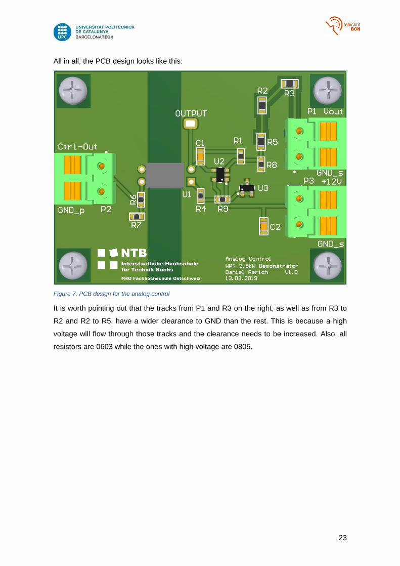
Once the measurements were obtained in the microcontroller, this data needed to be sent
to the transmitter side. This was done through 2 Wi-Fi modules, based on the RN-131G
from Roving Networks. These modules have been chosen because they are already used
for another subject at the NTB, so they were available and easy to configure. The schematic
of those modules can be found in the appendices.
Figure 8. Wi-Fi Module
In the transmitter side, an experimenter kit C2000 Launchpad XL was used, in particular
the TMS320F280049C. The one in the receiver side could not be used since it does not
have a DAC.
Having the data in the transmitter side, the DAC generates a voltage proportional to the
received value, and with the circuit from the analog control the frequency is modulated.
Two PCB have been designed to fulfill the objective: one for the receiver side and another
for the transmitter side.
25
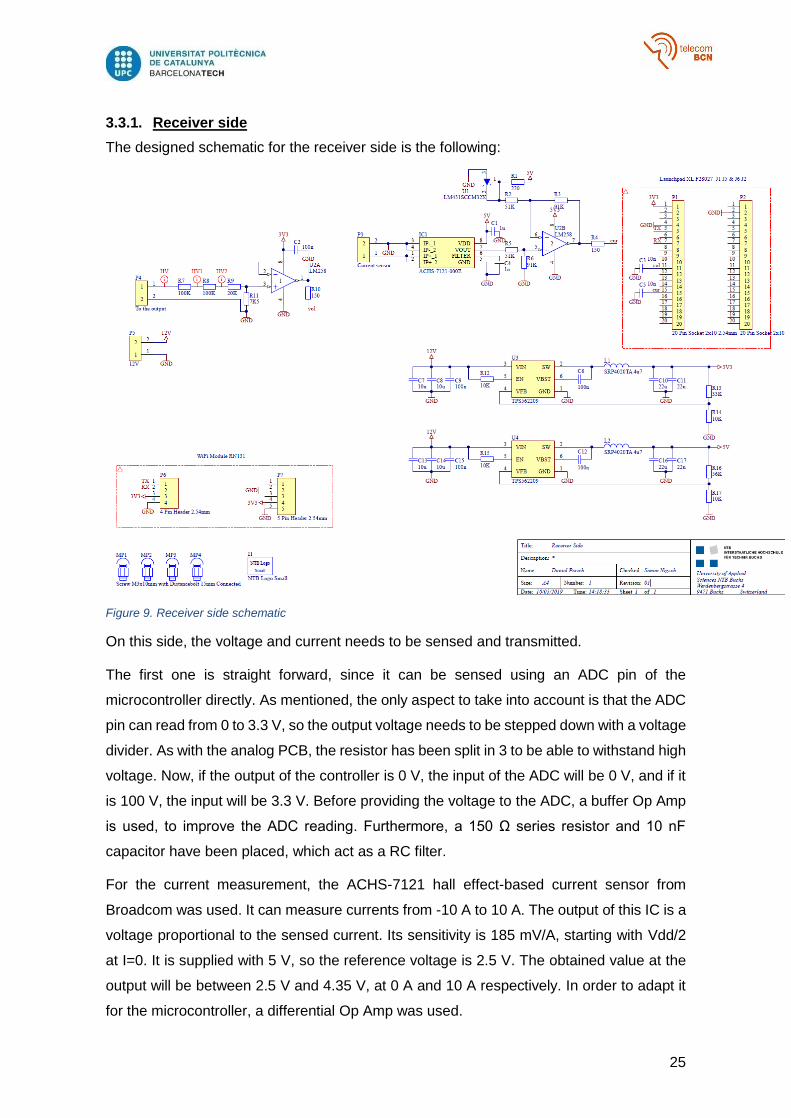
3.3.1. Receiver side
The designed schematic for the receiver side is the following:
Figure 9. Receiver side schematic
On this side, the voltage and current needs to be sensed and transmitted.
The first one is straight forward, since it can be sensed using an ADC pin of the
microcontroller directly. As mentioned, the only aspect to take into account is that the ADC
pin can read from 0 to 3.3 V, so the output voltage needs to be stepped down with a voltage
divider. As with the analog PCB, the resistor has been split in 3 to be able to withstand high
voltage. Now, if the output of the controller is 0 V, the input of the ADC will be 0 V, and if it
is 100 V, the input will be 3.3 V. Before providing the voltage to the ADC, a buffer Op Amp
is used, to improve the ADC reading. Furthermore, a 150 Ω series resistor and 10 nF
capacitor have been placed, which act as a RC filter.
For the current measurement, the ACHS-7121 hall effect-based current sensor from
Broadcom was used. It can measure currents from -10 A to 10 A. The output of this IC is a
voltage proportional to the sensed current. Its sensitivity is 185 mV/A, starting with Vdd/2
at I=0. It is supplied with 5 V, so the reference voltage is 2.5 V. The obtained value at the
output will be between 2.5 V and 4.35 V, at 0 A and 10 A respectively. In order to adapt it
for the microcontroller, a differential Op Amp was used.

26
The output voltage should be 3.3 V when the current is 10 A, so taking the differential Op
Amp formula when the resistors on the inverting input are the same as the ones in the non-
inverting one:
𝑉𝑜𝑢𝑡 =𝑅3
𝑅2
(𝑉2 − 𝑉1)
Vout is 3.3 V and V1 is the reference voltage at 0 A, which is 2.5 V. In order to obtain the 2.5
V, the LM431 was used, the same IC used in the analog design. The 3.3 V at the output
should be obtained when V2 is maximum (at 10 A = 4.35 V), so the difference will be 4.35
– 2.5 = 1.85. Then,
𝑅3
𝑅2=
3.3
1.85= 1.7838 → 𝑅3 = 𝑅6 = 91 kΩ & R2 = 𝑅5 = 51 kΩ
At the output, a 150 Ω resistor and 10 nF capacitor were placed to filter the signal and
improve the readings.
Moreover, this PCB has headers to connect the Wi-Fi module and the evaluation kit of the
microcontroller, with the required connections. The readings are sent via the TX pin.
In order to get 3.3 V to supply the microcontroller, and 5 V to supply the Op Amps and
current sensors, another IC needed to be used.
One option was the MAX1615EUK, from Maxim. The particularity of this IC wa that it allows
to get 3.3 V and 5 V at the output only by connecting a pin to GND or to a high value,
respectively. However, this option was soon discarded because there were considerable
losses (from 12 V to 3.3 V) and the footprint of the component was very small, so it would
not have worked appropriately.
The second and definite option was to use a buck converter, in particular the TPS562209.
It can step down voltages from 4.5 V to 17 V to a range of 0.76 V to 7 V. In this case, 12 V
will be stepped down to 3.3 and 5 V. The design parameters are the specified on the
datasheet, except for the output resistors which adjust the output voltage. The formula is:
𝑉𝑜𝑢𝑡 = 0.765 · (1 +𝑅1
𝑅2)
Being R1 the resistor on top of the voltage divider and R2 the one on the bottom.
It is easy to obtain that, for 3.3 V output, 𝑅1 = 33 kΩ & R2 = 10 kΩ and for 5 V output,
𝑅1 = 56 kΩ & R2 = 10 kΩ.
27
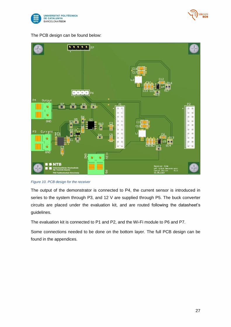
The PCB design can be found below:
Figure 10. PCB design for the receiver
The output of the demonstrator is connected to P4, the current sensor is introduced in
series to the system through P3, and 12 V are supplied through P5. The buck converter
circuits are placed under the evaluation kit, and are routed following the datasheet’s
guidelines.
The evaluation kit is connected to P1 and P2, and the Wi-Fi module to P6 and P7.
Some connections needed to be done on the bottom layer. The full PCB design can be
found in the appendices.
28
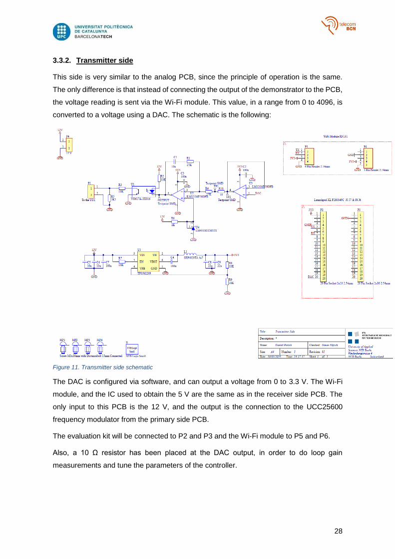
3.3.2. Transmitter side
This side is very similar to the analog PCB, since the principle of operation is the same.
The only difference is that instead of connecting the output of the demonstrator to the PCB,
the voltage reading is sent via the Wi-Fi module. This value, in a range from 0 to 4096, is
converted to a voltage using a DAC. The schematic is the following:
Figure 11. Transmitter side schematic
The DAC is configured via software, and can output a voltage from 0 to 3.3 V. The Wi-Fi
module, and the IC used to obtain the 5 V are the same as in the receiver side PCB. The
only input to this PCB is the 12 V, and the output is the connection to the UCC25600
frequency modulator from the primary side PCB.
The evaluation kit will be connected to P2 and P3 and the Wi-Fi module to P5 and P6.
Also, a 10 Ω resistor has been placed at the DAC output, in order to do loop gain
measurements and tune the parameters of the controller.
29
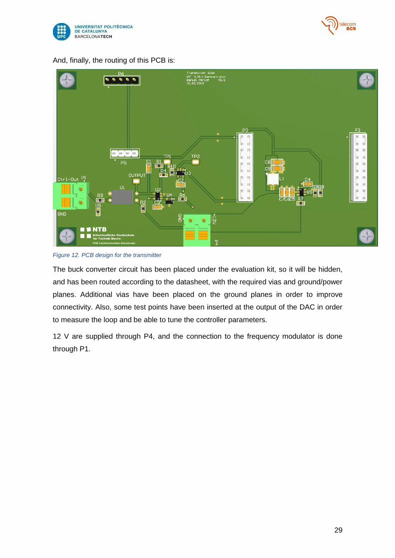
And, finally, the routing of this PCB is:
Figure 12. PCB design for the transmitter
The buck converter circuit has been placed under the evaluation kit, so it will be hidden,
and has been routed according to the datasheet, with the required vias and ground/power
planes. Additional vias have been placed on the ground planes in order to improve
connectivity. Also, some test points have been inserted at the output of the DAC in order
to measure the loop and be able to tune the controller parameters.
12 V are supplied through P4, and the connection to the frequency modulator is done
through P1.

30
3.3.3. Code
In order to write the microcontroller code for both the receiver and transmitter side, example
codes from Texas Instruments were used. In particular, for the receiver side, the example
codes used were “scia_loopback” and “adc_soc”, to establish the SCI communication and
read values from the ADC respectively. These examples can be found in the f2802x folder.
For the transmitter side, the examples codes “dac” and “sci” from the f28004x folder were
used. All these example codes are part of the C2000 Ware software.
The full code can be found in the appendices. The main functionality will be explained here.
Receiver side
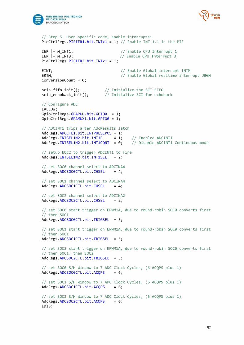
Firstly, all the needed initializations are done. This includes System Control, GPIO, PIE
interrupts, Flash, ADC, SCI.
The first main modification from the example code was to change the sampling frequency
of the ADC. Originally it was set to 0xFFFF, and since the microcontroller has a 60 MHz
clock it meant a frequency of 𝑓 =60·106
216−1= 915,54 Hz. The desired frequency was 10 kHz,
which gives a value of 60·106
10·103 = 6000. In hexadecimal, 6000 equals 0x1770.
However, when observing the PWM signal with an oscilloscope, the frequency was 5 kHz,
so finally the register value was 0x0BB8 (the half) to get a real frequency of 10 kHz.
EPwm1Regs.TBPRD = 0x0BB8; // Set period for ePWM1 0x1770 ->5 kHz (should be 10) // 10 kHz -> 0x0BB8
The for loop in the main program is one of the key parts of the code.
for(;;) { if (ConversionCount == 399) { vol = 0; cur = 0; for (i = 0; i < 400; i++) { vol += Voltage[i]; cur += Current[i]; } vol = vol / 400; cur = cur / 400; if (vol > 0 && vol < 4096 && cur > 0 && cur < 4096) { scia_xmit('s'); scia_xmit((vol >> 8) & 0xFF); //8 high bits scia_xmit(vol); //8 low bits scia_xmit((cur >> 8) & 0xFF); scia_xmit(cur); } }
}

31
The idea is quite simple. The ADC takes 400 samples, using an ISR which will be explained
later. Given that the sampling frequency is 10 kHz, the required time to take the samples
is 1
10·103 · 400 = 40 ms. This is because the Wi-Fi modules proved unreliable for lower
latency. With all the values stored in two arrays, one for the voltage values and another for
current values, the mean is done to increase accuracy.
Once the voltage and current values are obtained, if they are reasonable values (between
1 and 4095, both included), they are sent through the serial interface.
In order to control the flow of data, a start character (‘s’) is sent first. Immediately after, the
voltage and current values are sent. They need to be split in 2, because the SCI can send
8 bits and 4095 is 12 bits. The 8 highest bits are sent first, by shifting the value 8 bits to the
right, and then multiplying by 0xFF (0b11111111) to limit the value to 8 bits. However, since
the highest value is 12 bits, the high bits will be maximum 4 (15 in decimal).
Then, the 8 low bits are sent. This can be done by sending the whole value, because the
SCI register already chooses the 8 low bits.
The same procedure applies to the current value.
Finally, the ISR is in charge of obtaining the voltage and current values.
__interrupt void adc_isr(void) { Voltage[ConversionCount] = AdcResult.ADCRESULT1; Current[ConversionCount] = AdcResult.ADCRESULT2; if (ConversionCount == 399) { ConversionCount = 0; } else { ConversionCount++; } // // Clear ADCINT1 flag reinitialize for next SOC // AdcRegs.ADCINTFLGCLR.bit.ADCINT1 = 1; // // Acknowledge interrupt to PIE // PieCtrlRegs.PIEACK.all = PIEACK_GROUP1; return;
}
It counts until 400 conversion count have been logged, storing a sample for every value in
an array. It also prepares the uC for the next interrupt by clearing the flag and
acknowledging the interrupt.

32
Finally, the default SCI transmission rate was 9600, and the Wi-Fi module was set to
115200. The datasheet provides a formula to calculate the required register value to
change the rate.
𝑆𝐶𝐼 𝐵𝑅𝑅 =𝐿𝑆𝑃𝐶𝐿𝐾
8 · 𝑆𝐶𝐼 𝐵𝐴𝑈𝐷− 1
For this particular uC, the LSPCLK is 15 MHz, so the value needs to be 15·106
8·115200− 1 = 15.27
The low nearest integer is 15, 0x000F in hexadecimal.
SciaRegs.SCIHBAUD = 0x0000; //115200 baud @LSPCLK = 15MHz (60 MHz SYSCLK)
SciaRegs.SCILBAUD = 0x000F; //9600 -> 0x00C2
Transmitter side
In this side, the code was a bit harder.
The uC is initialized similarly. The ADC is not used in this side, but the DAC is used.
The configuration of the DAC needed to be adjusted to obtain a DAC value from 0 to 3.3 V
using the internal reference of 1.65 V and a gain of 2. This was done by checking a table
in the datasheet, which stated that the registers had to be configured this way:
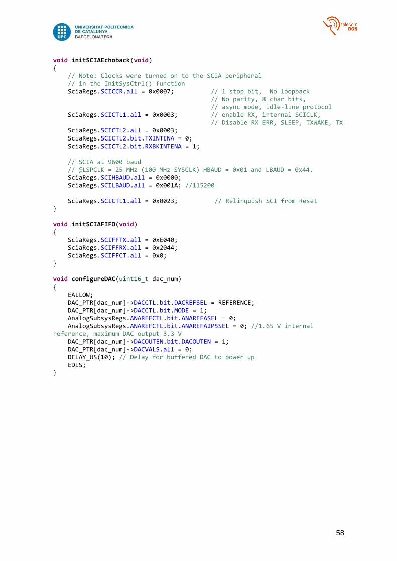
void configureDAC(uint16_t dac_num) { EALLOW; DAC_PTR[dac_num]->DACCTL.bit.DACREFSEL = REFERENCE; DAC_PTR[dac_num]->DACCTL.bit.MODE = 1; AnalogSubsysRegs.ANAREFCTL.bit.ANAREFASEL = 0; AnalogSubsysRegs.ANAREFCTL.bit.ANAREFA2P5SEL = 0; //1.65 V internal reference, maximum DAC output 3.3 V DAC_PTR[dac_num]->DACOUTEN.bit.DACOUTEN = 1; DAC_PTR[dac_num]->DACVALS.all = 0; DELAY_US(10); // Delay for buffered DAC to power up EDIS;
}
Where REFERENCE equals 0 when using an external reference and 1 when using the
internal one (1.65 V or 2.5 V).
The SCI needed to be adjusted the same way as before, but LSPCLK is 25 MHz for this
uC. Doing the calculations, the value is 26, which is 0x001A in hexadecimal.
// SCIA at 9600 baud // @LSPCLK = 25 MHz (100 MHz SYSCLK) HBAUD = 0x0001 and LBAUD = 0x0044. SciaRegs.SCIHBAUD.all = 0x0000;
SciaRegs.SCILBAUD.all = 0x001A; //115200 baud

33
The main for loop contains the following:
for(;;) { cnt = 0; while (SciaRegs.SCIRXBUF.all != 's'); while (SciaRegs.SCIFFRX.bit.RXFFST != 1 && cnt < 1000) { cnt++; } if (cnt == 1000) { continue; } vol_high = SciaRegs.SCIRXBUF.all; //RECEIVE THE 8 MSB FOR THE VOLTAGE cnt = 0; ... //REPEAT FOR THE 8 LSB FOR THE VOLTAGE AND BOTH CURRENT VALUES vol = vol_high << 8 | vol_low; cur = cur_high << 8 | cur_low; vout = vol * 3.3 / 4096; //from 0 to 3.3 V iout = (cur * (3.3 / 4096)-0.0642) / 0.343; //From V to A conversion if (vol > 0 && vol < 4096) { DAC_PTR[DAC_NUM]->DACVALS.all = vol; DELAY_US(2); } else { DAC_PTR[DAC_NUM]->DACVALS.all = 0; DELAY_US(2); error++; } } }
The uC stops the program until an ‘s’ is received. Afterwards, all the voltage and current
values are received, waiting for each value for the receiver to be ready. An additional
counter has been placed, so that if something goes wrong, the program does not get stuck
at that point. If after 1000 counts no value has been received, that iteration ends and a new
one starts, by using the instruction continue.
Then, the voltage and current values are put together by doing the inverse operation
(shifting 8 bits to the left and adding the 8 LSB).
Finally, if the voltage value received is within the normal range, a voltage proportional to
that value is output through the DAC pin, with a 2 µs delay recommended by the
manufacturer. If it is not right, the DAC outputs 0 V and increases an error counter.
The formula used to calculate the output current was obtained by calibrating the current
sensor, which will be explained in the next chapter.
34
4. Results
4.1. Simulation
The first step was to try the current system, in order to better understand its operation. The
first simulation run showed the following results:
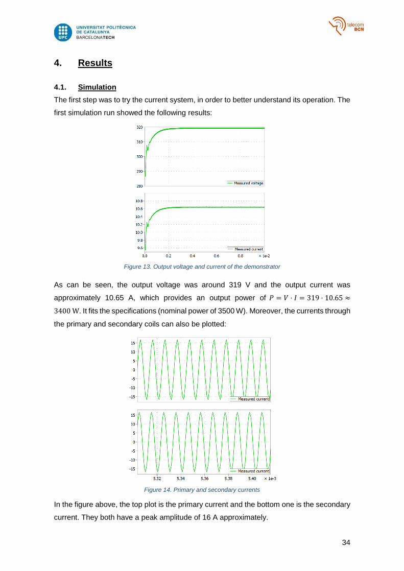
Figure 13. Output voltage and current of the demonstrator
As can be seen, the output voltage was around 319 V and the output current was
approximately 10.65 A, which provides an output power of 𝑃 = 𝑉 · 𝐼 = 319 · 10.65 ≈
3400 W. It fits the specifications (nominal power of 3500 W). Moreover, the currents through
the primary and secondary coils can also be plotted:
Figure 14. Primary and secondary currents
In the figure above, the top plot is the primary current and the bottom one is the secondary
current. They both have a peak amplitude of 16 A approximately.
35
The output power depends on the switching frequency, and also on the leakage and
magnetizing inductances. In order to find out the optimum frequency for every position of
the demonstrator, several tests were run. The obtained results can be found below:
Table 2. Optimum switching frequency for every position of the demonstrator
Air gap [mm] 50 105 160
Misalignment
[mm]
0 50 100 0 50 100 0 50 100
𝐿𝑝 [µH] 266.9 267.2 273.6 278.3 279.5 283.7 286.5 287.3 288.1
𝐿𝑚 [µH] 41.2 41.9 41.6 28.9 28.3 25.9 20.1 19.5 17.3
𝐿𝑠 [µH] 274.2 270.6 271.6 277.8 279.8 288.6 305.4 307.7 316.3
f [kHz] 97 97 96 96 96 94 99 99 98
𝑃𝑜𝑢𝑡 [W] 3400 3200 2960 3380 3490 3300 3420 3150 3410
The tests were run sweeping the operating frequency from 94 to 112 kHz. The goal was to
obtain the output power closest to 3500 W.
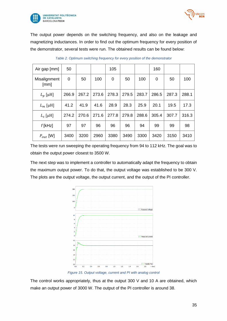
The next step was to implement a controller to automatically adapt the frequency to obtain
the maximum output power. To do that, the output voltage was established to be 300 V.
The plots are the output voltage, the output current, and the output of the PI controller.
Figure 15. Output voltage, current and PI with analog control
The control works appropriately, thus at the output 300 V and 10 A are obtained, which
make an output power of 3000 W. The output of the PI controller is around 38.
36
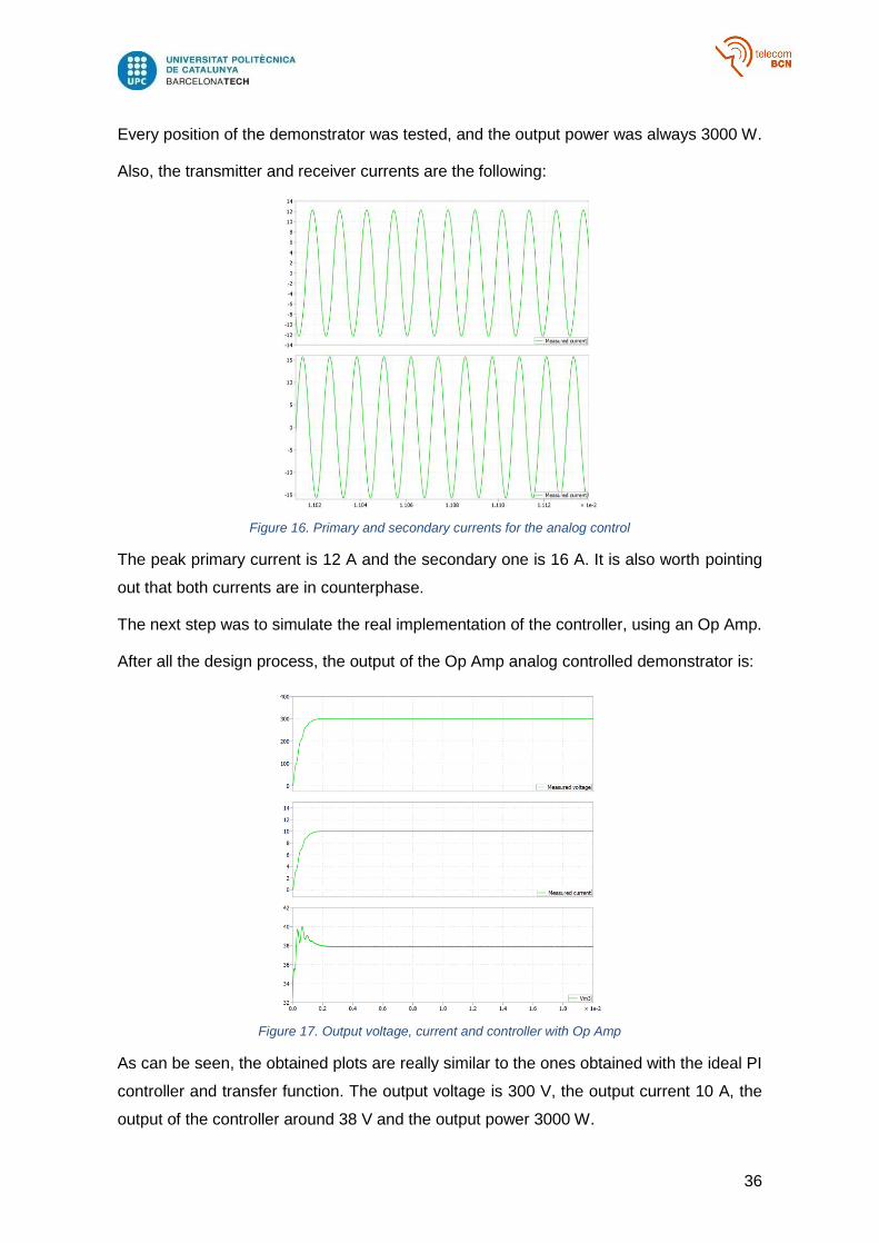
Every position of the demonstrator was tested, and the output power was always 3000 W.
Also, the transmitter and receiver currents are the following:
Figure 16. Primary and secondary currents for the analog control
The peak primary current is 12 A and the secondary one is 16 A. It is also worth pointing
out that both currents are in counterphase.
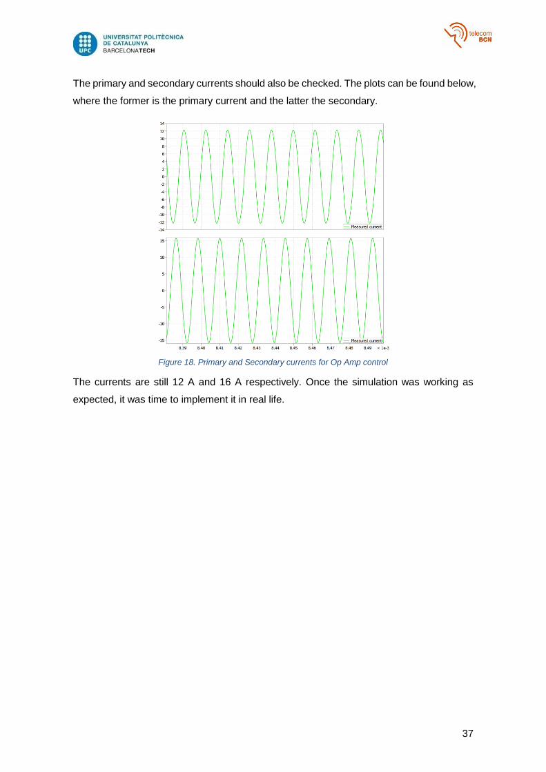
The next step was to simulate the real implementation of the controller, using an Op Amp.
After all the design process, the output of the Op Amp analog controlled demonstrator is:
Figure 17. Output voltage, current and controller with Op Amp
As can be seen, the obtained plots are really similar to the ones obtained with the ideal PI
controller and transfer function. The output voltage is 300 V, the output current 10 A, the
output of the controller around 38 V and the output power 3000 W.
37
The primary and secondary currents should also be checked. The plots can be found below,
where the former is the primary current and the latter the secondary.
Figure 18. Primary and Secondary currents for Op Amp control
The currents are still 12 A and 16 A respectively. Once the simulation was working as
expected, it was time to implement it in real life.

38
4.2. PCB Design for Analog Control
The PCB was manufactured and soldered as explained in the Design section. However,
when trying it, it was not working as expected. Some changes in the design had to be done.
First, the PCB was tested with an output voltage of 30 V, so the resistor in the voltage
divider at the output needed to be changed from 4,7 kΩ to 51 kΩ. The controller did not
control very well for every position of the demonstrator, so the Op Amp loop components
were modified from 6.8 nF and 56 kΩ to 100 nF and 5.6 kΩ. Even so, the controller was
not working properly. After some verifications, it was clear that the switching frequency was
limited, and in order to widen the range, the 13 kΩ resistor at the left was replaced by a 10
kΩ resistor. Also, just to be sure, the resistor at the diode in the optocoupler was changed
to have more current. The designed value was 43 kΩ and the actual value is 33 kΩ.
The new control function of the system is:
𝐺𝑐(𝑠) =5.6 · 103
560 · 103+
15.6 · 103 ∗ 100 · 10−9
𝑠= 0.01 +
1785.714
𝑠
Finally, the output voltage was increased to 100 V and the system kept that output for
every position of the coils. With a working controller, the microcontroller design for
wireless data transmission could be started.

39
4.3. Microcontroller
This design also needed a few changes when implementing it.
In the transmitter side, the optocoupler did not work appropriately because there was not
enough current flowing. This was solved by decreasing R2 from 33 kΩ to 10 kΩ. However,
this extra current caused a limitation in the switching frequency of the MOSFETs, since the
frequency limits are calculated using the current flowing out of the RT pin of the UCC25600.
The resistor limiting the maximum frequency, R3, changed from 10 kΩ to 2 kΩ and the one
for the minimum frequency was 2.2 kΩ and now is 2 kΩ. With those changes, the frequency
range of the MOSFETs is 100 – 150 kHz. Moreover, the controller did not control
appropriately so its parameters were changed from 10 nF and 27 kΩ to 22 µF and 270 Ω.
The cause was that this new control is a completely different one than the previous one
because it sends and receives data wirelessly, slowing down the system.
As for the receiver side, the only needed change was to supply the Op Amp at 12 V instead
of 3.3 V. That is because the voltage range of this particular IC is from 0 to VCC – 1.5 V,
and therefore it was not able to output the required voltage.
The PCBs were first tried for 30 V output and 75 V input, then 70 V output 100 V input and
finally 100 V output and 120 V input.
Code problem
At first, the receiver side microcontroller (F280049C) needed the reset button to be pressed
in order to start the control. At first, this problem was tried to be solved using a RC filter to
force a low state when starting the uC, but it did not work. The working solution was to add
some lines of code at the beginning of the program:
DELAY_US(4000000); SciaRegs.SCICTL1.bit.SWRESET = 0; SciaRegs.SCICTL1.bit.SWRESET = 1;
As can be seen, the culprit was the SCI. Probably the cause was that the Wi-Fi modules
need around 4 seconds to connect to each other when turning them on, and that stopped
the program at a while loop. To avoid it, a 4 second delay was placed, and a software reset
was performed to the uC, in particular to the SCI module.
40
Current sensor calibration
The current measurement was not used to control the system, only the voltage. However,
the design integrated a current sensor. The current values obtained using the theoretical
sensitivity (330 mV/A) did not match the expected ones, so calibration was needed in the
code. To test it, the power supply was connected to the PCB and the ADC from the uC
read voltage values proportional to those currents: 𝑖 = 𝐴𝐷𝐶 𝑣𝑎𝑙𝑢𝑒 ∗3.3
4096∗
1
0.33
The results can be observed in the table below:
Table 3. Current readings and voltage measurements without calibration
Supplied (A) 0 1 2 3 4 5 6 7 8 9
Measured (A) 0.13 1.17 2.22 3.25 4.28 5.33 6.36 7.38 8.41 9.43
Error (A) 0.13 0.17 0.22 0.25 0.28 0.33 0.36 0.38 0.41 0.43
Voltage (V) 0.0642 0.4147 0.7561 1.0974 1.4393 1.7812 2.124 2.4661 2.8084 3.1515
To calibrate it, the procedure was the following:
1. Subtract the offset (voltage at 0 A)
2. Calculate the new sensitivity
So, the new sensitivity was:
𝑠𝑒𝑛𝑠𝑖𝑡𝑖𝑣𝑖𝑡𝑦 =𝑣𝑜𝑙𝑡𝑎𝑔𝑒 − 0.0642
𝑐𝑢𝑟𝑟𝑒𝑛𝑡=
3.1515 − 0.0642
9= 0.343 𝑉
𝐴⁄
Therefore, in the code, the current measurement is:
iout= (cur * (3.3 / 4096)-0.0642) / 0.343; //From ADC to A conversion
And the current values after correction:
Table 4. Current readings with calibration
Supplied (A) 0 1 2 3 4 5 6 7 8 9
Measured (A) 0.005 1 2.02 3 3.99 5.01 6 6.99 7.98 8.97
Error (A) 0.005 0 0.02 0 -0.01 0.01 0 -0.01 -0.02 -0.03
As can be seen, the accuracy improved dramatically.
41
Results
The control function of the final design is:
𝐺𝑐(𝑠) =270
27 · 103+
122 · 10−6 ∗ 270
𝑠= 0.01 +
168.35
𝑠
The whole working system looks like this:
Figure 19. Whole system operating
In the transmitter side (bottom) there is the primary side PCB, which is supplied at 120 V
from the power supply, the transmitter side PCB, with the experimenter kit of the uC and
the Wi-Fi module, and the fixed coil.
In the receiver side (top), there is the mobile coil, the secondary side PCB and the receiver
side PCB, which includes the experimenter kit of the uC and the Wi-Fi module.
The input voltage and current are 120 V and 2.81 A and the output ones 100 V and 2.77 A
The output of the demonstrator, observed in an oscilloscope, is the following:
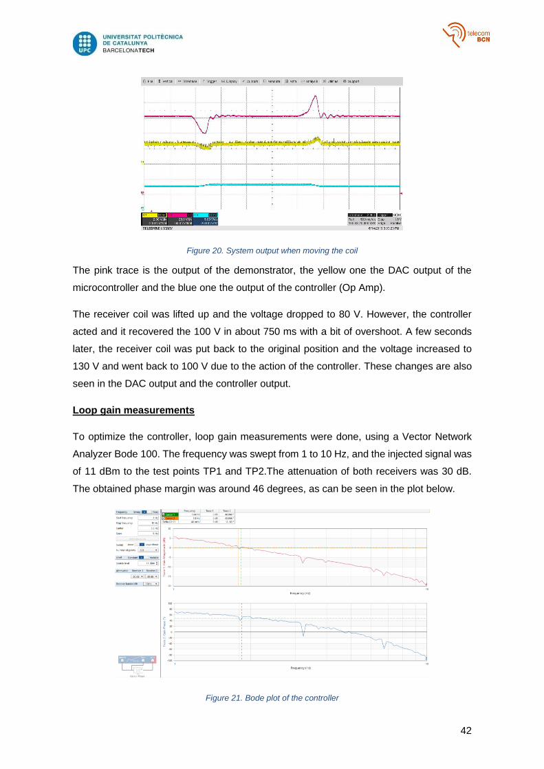
42
Figure 20. System output when moving the coil
The pink trace is the output of the demonstrator, the yellow one the DAC output of the
microcontroller and the blue one the output of the controller (Op Amp).
The receiver coil was lifted up and the voltage dropped to 80 V. However, the controller
acted and it recovered the 100 V in about 750 ms with a bit of overshoot. A few seconds
later, the receiver coil was put back to the original position and the voltage increased to
130 V and went back to 100 V due to the action of the controller. These changes are also
seen in the DAC output and the controller output.
Loop gain measurements
To optimize the controller, loop gain measurements were done, using a Vector Network
Analyzer Bode 100. The frequency was swept from 1 to 10 Hz, and the injected signal was
of 11 dBm to the test points TP1 and TP2.The attenuation of both receivers was 30 dB.
The obtained phase margin was around 46 degrees, as can be seen in the plot below.
Figure 21. Bode plot of the controller

43
The recommended value is around 60 degrees to be stable, so to improve it, the
capacitor in the Op Amp loop was modified from 22 µF to 44 µF. Also, the gain was
increased by changing the resistor in series from 270 Ω to 620 Ω and the one
outside the loop from 27 kΩ to 20 kΩ. The results were:
Figure 22. Bode plot of the system with modified parameters
At this moment, the phase margin increased to 73 degrees but the bandwidth
dropped noticeably from 1.84 Hz to 1.04 Hz. Observing the trace, the gain
magnitude at the point where the phase is 60 degrees was around -4 or 5 dB. The
proportional gain of the controller was increased to improve the bandwidth
maintaining the phase margin. That means that those dB need to be compensated
in the proportional gain, without modifying the loop:
4.5 dB = 20 · log(20000) − 20 · log(𝑥) → 𝑥 = 104.5−20·log(20000)
−20 = 11913 Ω
In view of the results, the resistor was changed from 20 kΩ to 12 kΩ. The final
transfer function after all the modifications is:
𝐺𝑐(𝑠) =620
12 · 103+
144 · 10−6 ∗ 620
𝑠= 0.0517 +
36.657
𝑠
44
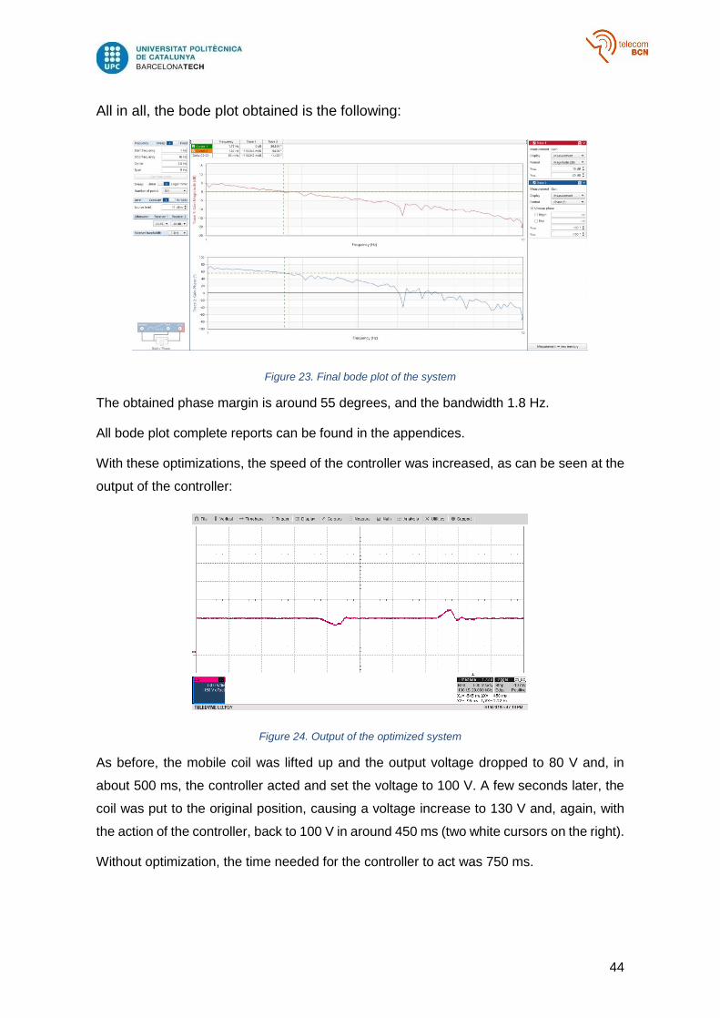
All in all, the bode plot obtained is the following:
Figure 23. Final bode plot of the system
The obtained phase margin is around 55 degrees, and the bandwidth 1.8 Hz.
All bode plot complete reports can be found in the appendices.
With these optimizations, the speed of the controller was increased, as can be seen at the
output of the controller:
Figure 24. Output of the optimized system
As before, the mobile coil was lifted up and the output voltage dropped to 80 V and, in
about 500 ms, the controller acted and set the voltage to 100 V. A few seconds later, the
coil was put to the original position, causing a voltage increase to 130 V and, again, with
the action of the controller, back to 100 V in around 450 ms (two white cursors on the right).
Without optimization, the time needed for the controller to act was 750 ms.
45
5. Budget
5.1. Analog Control
All the required components to do the analog control PCB were already in the lab, so I
made an estimation of the price they would cost if they needed to be ordered.
Table 5. Component list for the analog control PCB
Index Units Part Number Description Unit
price (€)
Total
price (€)
1 10 CRGCQ0603J2K2 2.2kΩ 1/10 W 0603 0.02 0.20
2 10 RMCF0603FT13K0 13kΩ 1/10 W 0603 0.016 0.16
3 10 RC0603JR-0743KL 43kΩ 1/10 W 0603 0.017 0.17
4 10 RMCF0603FT56K0 56kΩ 1/10 W 0603 0.016 0.16
5 10 RR1220P-184-D 180kΩ 1/10 W 0805 0.086 0.86
6 10 RR1220P-204-D 200kΩ 1/10 W 0805 0.086 0.86
7 10 RC0603JR-074K7L 4.7kΩ 1/10 W 0603 0.017 0.17
8 10 RMCF0603FT1K00 1kΩ 1/10 W 0603 0.016 0.16
9 5 CC0805KKX7RYBB682 6.8nF 250V X7R 0805 0.17 0.85
10 5 CC0805KRX7R9BB104 100nF 50V X7R 0805 0.14 0.70
11 3 VO617A-3X016 Optoisolator 0.63 1.89
12 3 LM321MF/NOPB IC OPAMP 0.57 1.71
13 3 LM431SCCM32X IC VREF SHUNT 0.41 1.23
14 5 COMBICON 1934861 2 pin phoenix contact 0.38 1.90
15 4 50M060100D016 Screw 10 mm 0.13 0.52
TOTAL 11.54 €
For the PCB manufacturing, the price was 64.50 €.
46
Moreover, in order to do the simulations and the design, PLECS and Altium Designer
were used. Those programs were provided by the university. The price for an academic
PLECS license is 1200 € and for an Altium license, the price is not public and is agreed
with the sales office. However, the price is expected to be over 3000 €.
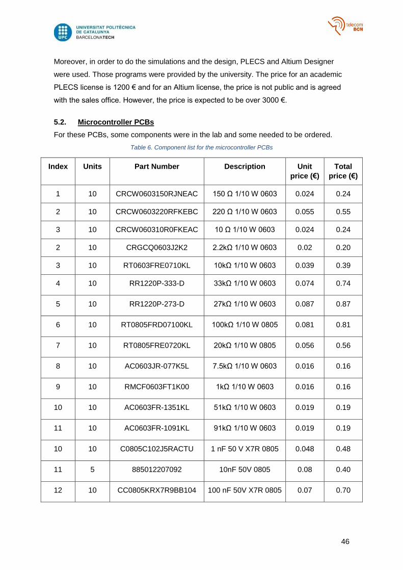
5.2. Microcontroller PCBs
For these PCBs, some components were in the lab and some needed to be ordered.
Table 6. Component list for the microcontroller PCBs
Index Units Part Number Description Unit
price (€)
Total
price (€)
1 10 CRCW0603150RJNEAC 150 Ω 1/10 W 0603 0.024 0.24
2 10 CRCW0603220RFKEBC 220 Ω 1/10 W 0603 0.055 0.55
3 10 CRCW060310R0FKEAC 10 Ω 1/10 W 0603 0.024 0.24
2 10 CRGCQ0603J2K2 2.2kΩ 1/10 W 0603 0.02 0.20
3 10 RT0603FRE0710KL 10kΩ 1/10 W 0603 0.039 0.39
4 10 RR1220P-333-D 33kΩ 1/10 W 0603 0.074 0.74
5 10 RR1220P-273-D 27kΩ 1/10 W 0603 0.087 0.87
6 10 RT0805FRD07100KL 100kΩ 1/10 W 0805 0.081 0.81
7 10 RT0805FRE0720KL 20kΩ 1/10 W 0805 0.056 0.56
8 10 AC0603JR-077K5L 7.5kΩ 1/10 W 0603 0.016 0.16
9 10 RMCF0603FT1K00 1kΩ 1/10 W 0603 0.016 0.16
10 10 AC0603FR-1351KL 51kΩ 1/10 W 0603 0.019 0.19
11 10 AC0603FR-1091KL 91kΩ 1/10 W 0603 0.019 0.19
10 10 C0805C102J5RACTU 1 nF 50 V X7R 0805 0.048 0.48
11 5 885012207092 10nF 50V 0805 0.08 0.40
12 10 CC0805KRX7R9BB104 100 nF 50V X7R 0805 0.07 0.70
47
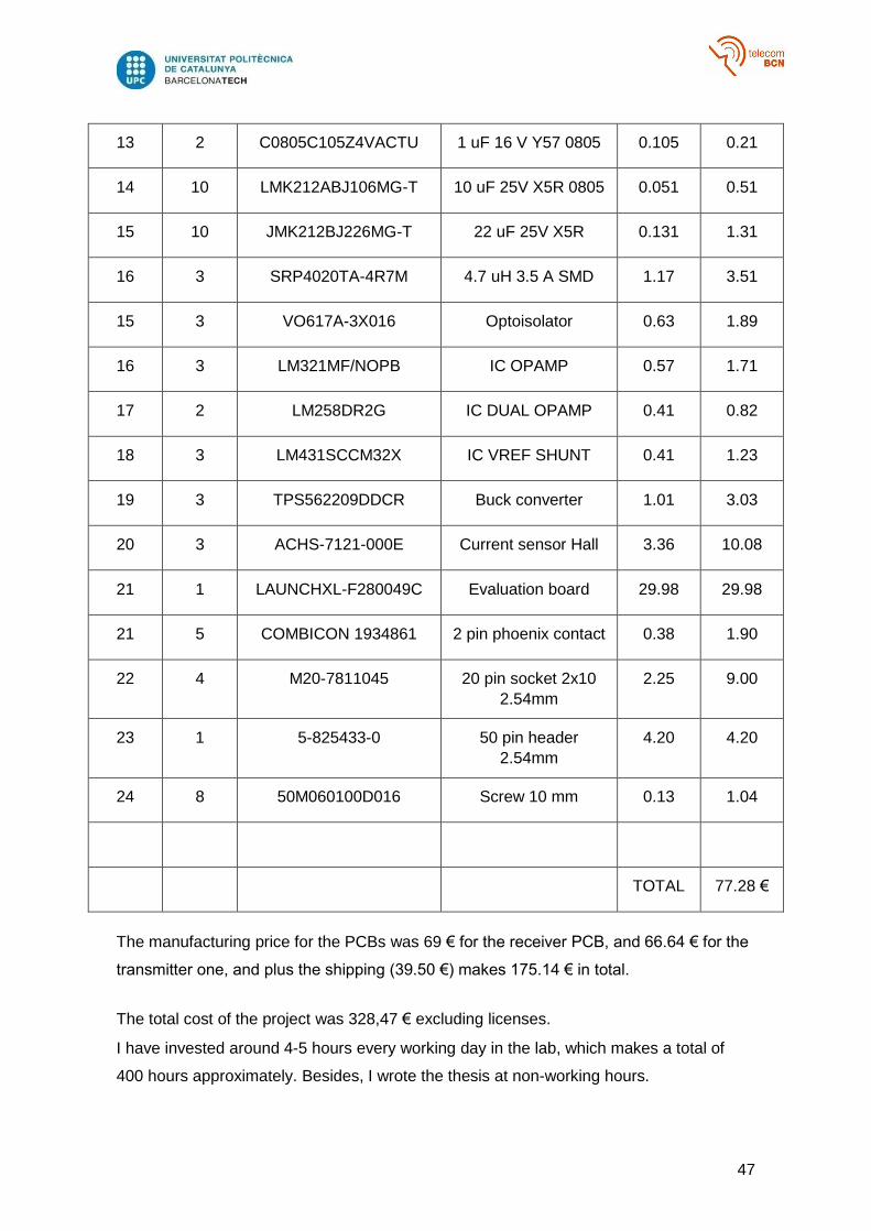
13 2 C0805C105Z4VACTU 1 uF 16 V Y57 0805 0.105 0.21
14 10 LMK212ABJ106MG-T 10 uF 25V X5R 0805 0.051 0.51
15 10 JMK212BJ226MG-T 22 uF 25V X5R 0.131 1.31
16 3 SRP4020TA-4R7M 4.7 uH 3.5 A SMD 1.17 3.51
15 3 VO617A-3X016 Optoisolator 0.63 1.89
16 3 LM321MF/NOPB IC OPAMP 0.57 1.71
17 2 LM258DR2G IC DUAL OPAMP 0.41 0.82
18 3 LM431SCCM32X IC VREF SHUNT 0.41 1.23
19 3 TPS562209DDCR Buck converter 1.01 3.03
20 3 ACHS-7121-000E Current sensor Hall 3.36 10.08
21 1 LAUNCHXL-F280049C Evaluation board 29.98 29.98
21 5 COMBICON 1934861 2 pin phoenix contact 0.38 1.90
22 4 M20-7811045 20 pin socket 2x10
2.54mm
2.25 9.00
23 1 5-825433-0 50 pin header
2.54mm
4.20 4.20
24 8 50M060100D016 Screw 10 mm 0.13 1.04
TOTAL 77.28 €
The manufacturing price for the PCBs was 69 € for the receiver PCB, and 66.64 € for the
transmitter one, and plus the shipping (39.50 €) makes 175.14 € in total.
The total cost of the project was 328,47 € excluding licenses.
I have invested around 4-5 hours every working day in the lab, which makes a total of
400 hours approximately. Besides, I wrote the thesis at non-working hours.

48
6. Conclusions and future development
The objective of the thesis has been achieved. The designed controller is able to control
the system at a fixed output voltage which does not depend on the position of the coils.
The controller has been tested for 120 V input and 100 V output. In spite of being functional,
the controller is slower than expected due to an unexpected delay in the data transmission.
Using loop gain measurements, the speed of the controller was improved from 750 ms to
500 ms, and the final bandwidth was 1.8 Hz.
As further development, the transmission medium could be changed to a different one
(Bluetooth, Infrared, GSM…), or even a different Wi-Fi module since it proved to be quite
slow (40 ms needed to be sure every packet arrives).
Moreover, the voltage could be increased to the one attained without control (380 V at the
input, around 260 V at the output). It was not done in this thesis due to the lack of
experience with such high voltages and the time constraint.
49
Bibliography
[1] Golnaraghi, F. and Kuo, B. (2009). Automatic control systems. Chichester: John Wiley & Sons.
[2] R. Haldi. “Wireless Battery Charger for Electric Cars”. M.S. thesis, Faculty of Power Electronics, University of Applied Sciences NTB Buchs, Buchs, Switzerland, 2014.
[3] R. Bosshard, “Multi-Objective Optimization of Inductive Power Transfer Systems for EV Charging,” Ph.D. dissertation, Department of Power Electronics, ETH University, Zurich, Switzerland, 2015.
[4] R. Haldi, K. Schenk, I. Nam and E. Santi, "Finite-element-simulation-assisted optimized design of an asymmetrical high-power inductive coupler with a large air gap for EV charging," 2013 IEEE Energy Conversion Congress and Exposition, Denver, CO, 2013, pp. 3635-3642.
[5] R. Haldi and K. Schenk, "A 3.5 kW wireless charger for electric vehicles with ultra-high efficiency," 2014 IEEE Energy Conversion Congress and Exposition (ECCE), Pittsburgh, PA, 2014, pp. 668-674.
[6] C. Chen, H. Zhou, Q. Deng and X. Luo, "Nonlinear modeling and feedback control of WPT system via magnetic resonant coupling considering continuous dynamic tuning," 2017 Chinese Automation Congress (CAC), Jinan, 2017, pp. 4203-4208.
[7] Pandu Wijaya, Febry & Kondo, Keiichiro. (2015). Charging power limitation method of a wireless power transmission system for railway vehicle. 003525-003530. 10.1109/IECON.2015.739264
[8] M.A. Saad Abdelhameed. “On-Chip Adaptive Power Management for WPT-Enabled IoT”. Ph.D. dissertation, Department of Power Electronics, Polytechnic University of Catalonia, Barcelona, 2018.
50
Appendices
1. Provided schematics
Figure 25. System Schematic
51
Figure 26. Wi-Fi Module Schematic
52
2. Analog design
Figure 27. Analog control schematic
Figure 28. PCB design for analog control, top layer
53
Figure 29. PCB design for analog control, bottom layer
54
3. Receiver side
Figure 30. Schematic for receiver side PCB
55
Figure 31. PCB design for the receiver, top layer
Figure 32. PCB design for the receiver, bottom layer
56
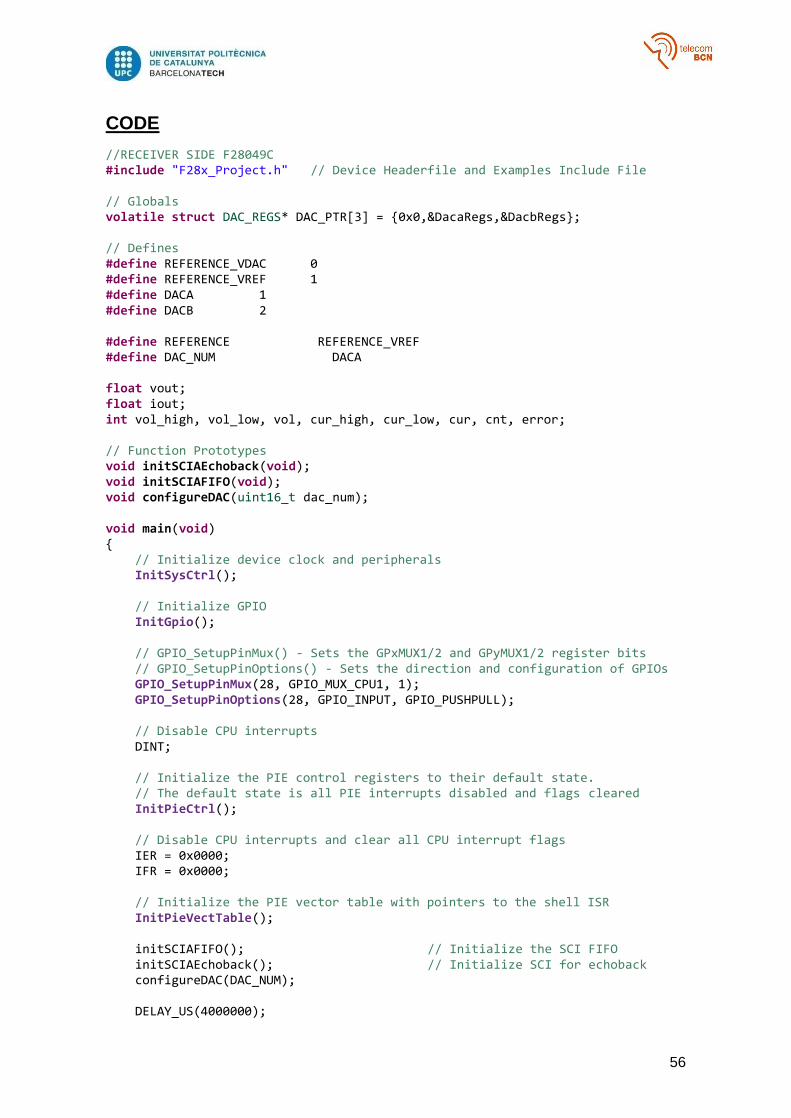
CODE
//RECEIVER SIDE F28049C #include "F28x_Project.h" // Device Headerfile and Examples Include File // Globals volatile struct DAC_REGS* DAC_PTR[3] = {0x0,&DacaRegs,&DacbRegs}; // Defines #define REFERENCE_VDAC 0 #define REFERENCE_VREF 1 #define DACA 1 #define DACB 2 #define REFERENCE REFERENCE_VREF #define DAC_NUM DACA float vout; float iout; int vol_high, vol_low, vol, cur_high, cur_low, cur, cnt, error; // Function Prototypes void initSCIAEchoback(void); void initSCIAFIFO(void); void configureDAC(uint16_t dac_num); void main(void) { // Initialize device clock and peripherals InitSysCtrl(); // Initialize GPIO InitGpio(); // GPIO_SetupPinMux() - Sets the GPxMUX1/2 and GPyMUX1/2 register bits // GPIO_SetupPinOptions() - Sets the direction and configuration of GPIOs GPIO_SetupPinMux(28, GPIO_MUX_CPU1, 1); GPIO_SetupPinOptions(28, GPIO_INPUT, GPIO_PUSHPULL); // Disable CPU interrupts DINT; // Initialize the PIE control registers to their default state. // The default state is all PIE interrupts disabled and flags cleared InitPieCtrl(); // Disable CPU interrupts and clear all CPU interrupt flags IER = 0x0000; IFR = 0x0000; // Initialize the PIE vector table with pointers to the shell ISR InitPieVectTable(); initSCIAFIFO(); // Initialize the SCI FIFO initSCIAEchoback(); // Initialize SCI for echoback configureDAC(DAC_NUM); DELAY_US(4000000);
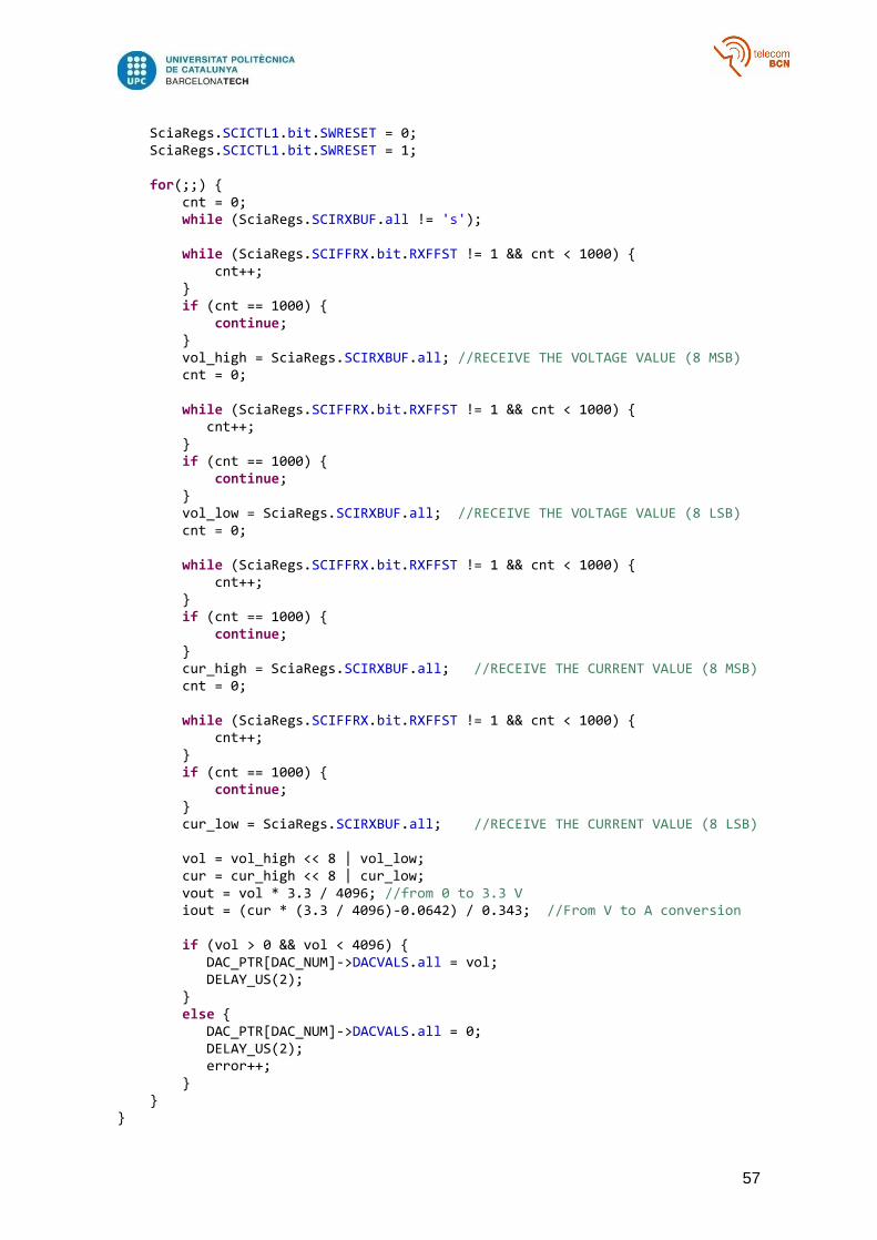
57
SciaRegs.SCICTL1.bit.SWRESET = 0; SciaRegs.SCICTL1.bit.SWRESET = 1; for(;;) { cnt = 0; while (SciaRegs.SCIRXBUF.all != 's'); while (SciaRegs.SCIFFRX.bit.RXFFST != 1 && cnt < 1000) { cnt++; } if (cnt == 1000) { continue; } vol_high = SciaRegs.SCIRXBUF.all; //RECEIVE THE VOLTAGE VALUE (8 MSB) cnt = 0; while (SciaRegs.SCIFFRX.bit.RXFFST != 1 && cnt < 1000) { cnt++; } if (cnt == 1000) { continue; } vol_low = SciaRegs.SCIRXBUF.all; //RECEIVE THE VOLTAGE VALUE (8 LSB) cnt = 0; while (SciaRegs.SCIFFRX.bit.RXFFST != 1 && cnt < 1000) { cnt++; } if (cnt == 1000) { continue; } cur_high = SciaRegs.SCIRXBUF.all; //RECEIVE THE CURRENT VALUE (8 MSB) cnt = 0; while (SciaRegs.SCIFFRX.bit.RXFFST != 1 && cnt < 1000) { cnt++; } if (cnt == 1000) { continue; } cur_low = SciaRegs.SCIRXBUF.all; //RECEIVE THE CURRENT VALUE (8 LSB) vol = vol_high << 8 | vol_low; cur = cur_high << 8 | cur_low; vout = vol * 3.3 / 4096; //from 0 to 3.3 V iout = (cur * (3.3 / 4096)-0.0642) / 0.343; //From V to A conversion if (vol > 0 && vol < 4096) { DAC_PTR[DAC_NUM]->DACVALS.all = vol; DELAY_US(2); } else { DAC_PTR[DAC_NUM]->DACVALS.all = 0; DELAY_US(2); error++; } } }
58
void initSCIAEchoback(void) { // Note: Clocks were turned on to the SCIA peripheral // in the InitSysCtrl() function SciaRegs.SCICCR.all = 0x0007; // 1 stop bit, No loopback // No parity, 8 char bits, // async mode, idle-line protocol SciaRegs.SCICTL1.all = 0x0003; // enable RX, internal SCICLK, // Disable RX ERR, SLEEP, TXWAKE, TX SciaRegs.SCICTL2.all = 0x0003; SciaRegs.SCICTL2.bit.TXINTENA = 0; SciaRegs.SCICTL2.bit.RXBKINTENA = 1; // SCIA at 9600 baud // @LSPCLK = 25 MHz (100 MHz SYSCLK) HBAUD = 0x01 and LBAUD = 0x44. SciaRegs.SCIHBAUD.all = 0x0000; SciaRegs.SCILBAUD.all = 0x001A; //115200 SciaRegs.SCICTL1.all = 0x0023; // Relinquish SCI from Reset } void initSCIAFIFO(void) { SciaRegs.SCIFFTX.all = 0xE040; SciaRegs.SCIFFRX.all = 0x2044; SciaRegs.SCIFFCT.all = 0x0; } void configureDAC(uint16_t dac_num) { EALLOW; DAC_PTR[dac_num]->DACCTL.bit.DACREFSEL = REFERENCE; DAC_PTR[dac_num]->DACCTL.bit.MODE = 1; AnalogSubsysRegs.ANAREFCTL.bit.ANAREFASEL = 0; AnalogSubsysRegs.ANAREFCTL.bit.ANAREFA2P5SEL = 0; //1.65 V internal reference, maximum DAC output 3.3 V DAC_PTR[dac_num]->DACOUTEN.bit.DACOUTEN = 1; DAC_PTR[dac_num]->DACVALS.all = 0; DELAY_US(10); // Delay for buffered DAC to power up EDIS; }
59
4. Transmitter side
Figure 33. Schematic for the transmitter PCB
Figure 34. PCB design for the transmitter, top layer
60
Figure 35. PCB design for the transmitter, bottom layer

61
CODE
//TRANSMITTER SIDE F28027 #include "DSP28x_Project.h" // Device Headerfile and Examples Include File __interrupt void adc_isr(void); void scia_echoback_init(void); void scia_fifo_init(void); void scia_xmit(int a); // Globals adc uint16_t ConversionCount; int Voltage[400]; int Current[400]; long vol, cur; int i; void main(void) { memcpy(&RamfuncsRunStart, &RamfuncsLoadStart, &RamfuncsLoadSize); // Step 1. Initialize System Control: // PLL, WatchDog, enable Peripheral Clocks // This example function is found in the f2802x_SysCtrl.c file. InitSysCtrl(); // Step 2. Initialize GPIO: // This example function is found in the f2802x_Gpio.c file and // illustrates how to set the GPIO to its default state. InitSciaGpio(); // Step 3. Clear all interrupts and initialize PIE vector table: DINT; // Disable CPU interrupts // Initialize the PIE control registers to their default state. // The default state is all PIE interrupts disabled and flags cleared // This function is found in the f2802x_PieCtrl.c file. InitPieCtrl(); // Clear all CPU interrupt flags IER = 0x0000; IFR = 0x0000; // Initialize the PIE vector table with pointers to the shell ISR // This will populate the entire table. This is useful for debug purposes. // The shell ISR routines are found in f2802x_DefaultIsr.c. // This function is found in f2802x_PieVect.c. InitPieVectTable(); InitFlash(); // Interrupts that are used in this example are re-mapped to // ISR functions found within this file EALLOW; // This is needed to write to EALLOW protected register PieVectTable.ADCINT1 = &adc_isr; EDIS; // This is needed to disable write to EALLOW protected registers // Step 4. Initialize all the Device Peripherals InitAdc(); // For this example, init the ADC AdcOffsetSelfCal();
62
// Step 5. User specific code, enable interrupts: PieCtrlRegs.PIEIER1.bit.INTx1 = 1; // Enable INT 1.1 in the PIE IER |= M_INT1; // Enable CPU Interrupt 1 IER |= M_INT3; // Enable CPU Interrupt 3 PieCtrlRegs.PIEIER3.bit.INTx1 = 1; EINT; // Enable Global interrupt INTM ERTM; // Enable Global realtime interrupt DBGM ConversionCount = 0; scia_fifo_init(); // Initialize the SCI FIFO scia_echoback_init(); // Initialize SCI for echoback // Configure ADC EALLOW; GpioCtrlRegs.GPAPUD.bit.GPIO0 = 1; GpioCtrlRegs.GPAMUX1.bit.GPIO0 = 1; // ADCINT1 trips after AdcResults latch AdcRegs.ADCCTL1.bit.INTPULSEPOS = 1; AdcRegs.INTSEL1N2.bit.INT1E = 1; // Enabled ADCINT1 AdcRegs.INTSEL1N2.bit.INT1CONT = 0; // Disable ADCINT1 Continuous mode // setup EOC2 to trigger ADCINT1 to fire AdcRegs.INTSEL1N2.bit.INT1SEL = 2; // set SOC0 channel select to ADCINA4 AdcRegs.ADCSOC0CTL.bit.CHSEL = 4; // set SOC1 channel select to ADCINA4 AdcRegs.ADCSOC1CTL.bit.CHSEL = 4; // set SOC2 channel select to ADCINA2 AdcRegs.ADCSOC2CTL.bit.CHSEL = 2; // set SOC0 start trigger on EPWM1A, due to round-robin SOC0 converts first // then SOC1 AdcRegs.ADCSOC0CTL.bit.TRIGSEL = 5; // set SOC1 start trigger on EPWM1A, due to round-robin SOC0 converts first // then SOC1 AdcRegs.ADCSOC1CTL.bit.TRIGSEL = 5; // set SOC2 start trigger on EPWM1A, due to round-robin SOC0 converts first // then SOC1, then SOC2 AdcRegs.ADCSOC2CTL.bit.TRIGSEL = 5; // set SOC0 S/H Window to 7 ADC Clock Cycles, (6 ACQPS plus 1) AdcRegs.ADCSOC0CTL.bit.ACQPS = 6; // set SOC1 S/H Window to 7 ADC Clock Cycles, (6 ACQPS plus 1) AdcRegs.ADCSOC1CTL.bit.ACQPS = 6; // set SOC2 S/H Window to 7 ADC Clock Cycles, (6 ACQPS plus 1) AdcRegs.ADCSOC2CTL.bit.ACQPS = 6; EDIS;
63
// Assumes ePWM1 clock is already enabled in InitSysCtrl(); EPwm1Regs.ETSEL.bit.SOCAEN = 1; // Enable SOC on A group // Select SOC from from CPMA on upcount EPwm1Regs.ETSEL.bit.SOCASEL = 4; EPwm1Regs.ETPS.bit.SOCAPRD = 1; // Generate pulse on 1st event EPwm1Regs.CMPA.half.CMPA = 0x0080; // Set compare A value EPwm1Regs.TBPRD = 0x0BB8; // Set period for ePWM1 1770->5 kHz (should be 10) // 10 kHz -> 0x0BB8 EPwm1Regs.TBCTL.bit.CTRMODE = 0; // count up and start EPwm1Regs.TBCTR = 0x0000; EPwm1Regs.AQCTLA.all = 0x0024; EALLOW; SysCtrlRegs.PCLKCR0.bit.TBCLKSYNC = 1; EDIS; // Wait for ADC interrupt for(;;) { if (ConversionCount == 399) { vol = 0; cur = 0; for (i = 0; i < 400; i++) { vol += Voltage[i]; cur += Current[i]; } vol = vol / 400; cur = cur / 400; if (vol > 0 && vol < 4096 && cur > 0 && cur < 4096) { scia_xmit('s'); scia_xmit((vol >> 8) & 0xFF); //8 high bits scia_xmit(vol); //8 low bits scia_xmit((cur >> 8) & 0xFF); scia_xmit(cur); } } } } __interrupt void adc_isr(void) { Voltage[ConversionCount] = AdcResult.ADCRESULT1; Current[ConversionCount] = AdcResult.ADCRESULT2; if (ConversionCount == 399) { ConversionCount = 0; } else { ConversionCount++; } // Clear ADCINT1 flag reinitialize for next SOC AdcRegs.ADCINTFLGCLR.bit.ADCINT1 = 1; // Acknowledge interrupt to PIE PieCtrlRegs.PIEACK.all = PIEACK_GROUP1; return; }
64
// scia_echoback_init - Test 1,SCIA DLB, 8-bit word, baud rate 0x000F, default // 1 STOP bit, no parity void scia_echoback_init() { // Note: Clocks were turned on to the SCIA peripheral // in the InitSysCtrl() function // 1 stop bit, No loopback, No parity, 8 char bits, async mode, // idle-line protocol SciaRegs.SCICCR.all =0x0007; // enable TX, internal SCICLK, Disable RX ERR, SLEEP, TXWAKE SciaRegs.SCICTL1.all =0x0003; SciaRegs.SCICTL2.all =0x0003; SciaRegs.SCICTL2.bit.TXINTENA =1; SciaRegs.SCICTL2.bit.RXBKINTENA = 0; SciaRegs.SCIFFTX.bit.SCIFFENA = 1; // SCI BRR = LSPCLK/(SCI BAUDx8) - 1 SciaRegs.SCIHBAUD = 0x0000; // 115200 baud @LSPCLK = 15MHz(60 MHz SYSCLK) SciaRegs.SCILBAUD = 0x000F; // 9600 -> 0x00C2 SciaRegs.SCICTL1.all =0x0023; // Relinquish SCI from Reset } void scia_xmit(int a) { while (SciaRegs.SCIFFTX.bit.TXFFST != 0); SciaRegs.SCITXBUF=a; } void scia_fifo_init() { SciaRegs.SCIFFTX.all=0xE040; SciaRegs.SCIFFRX.all=0x2044; SciaRegs.SCIFFCT.all=0x0; }
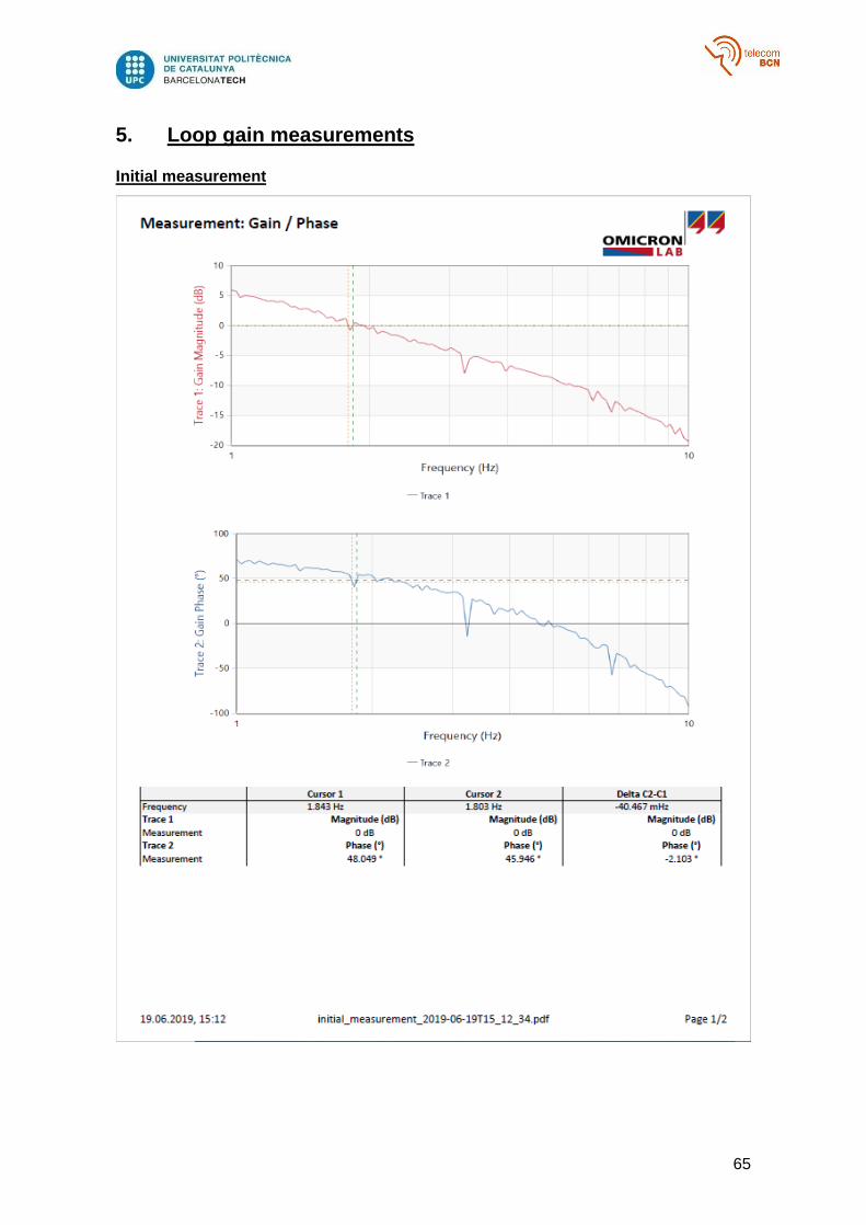
65
5. Loop gain measurements
Initial measurement
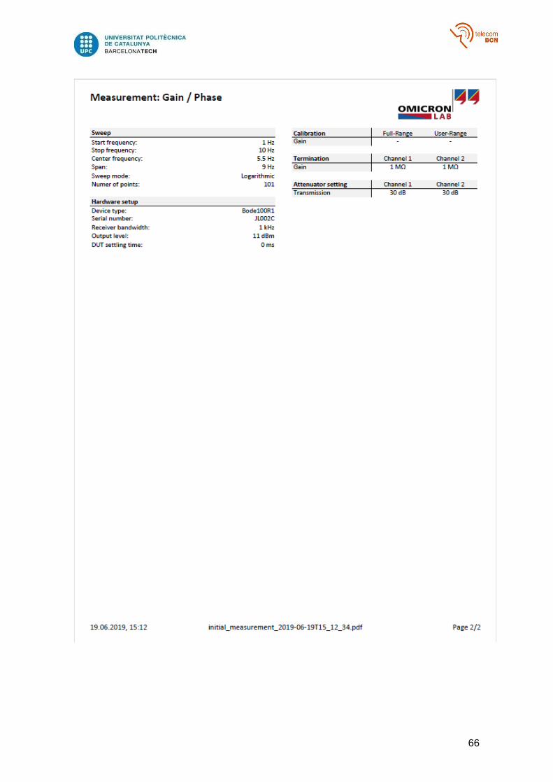
66
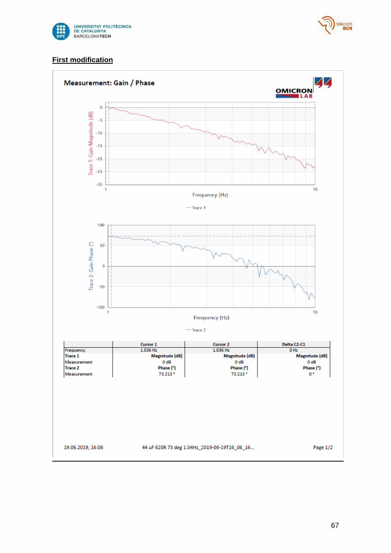
67
First modification
68
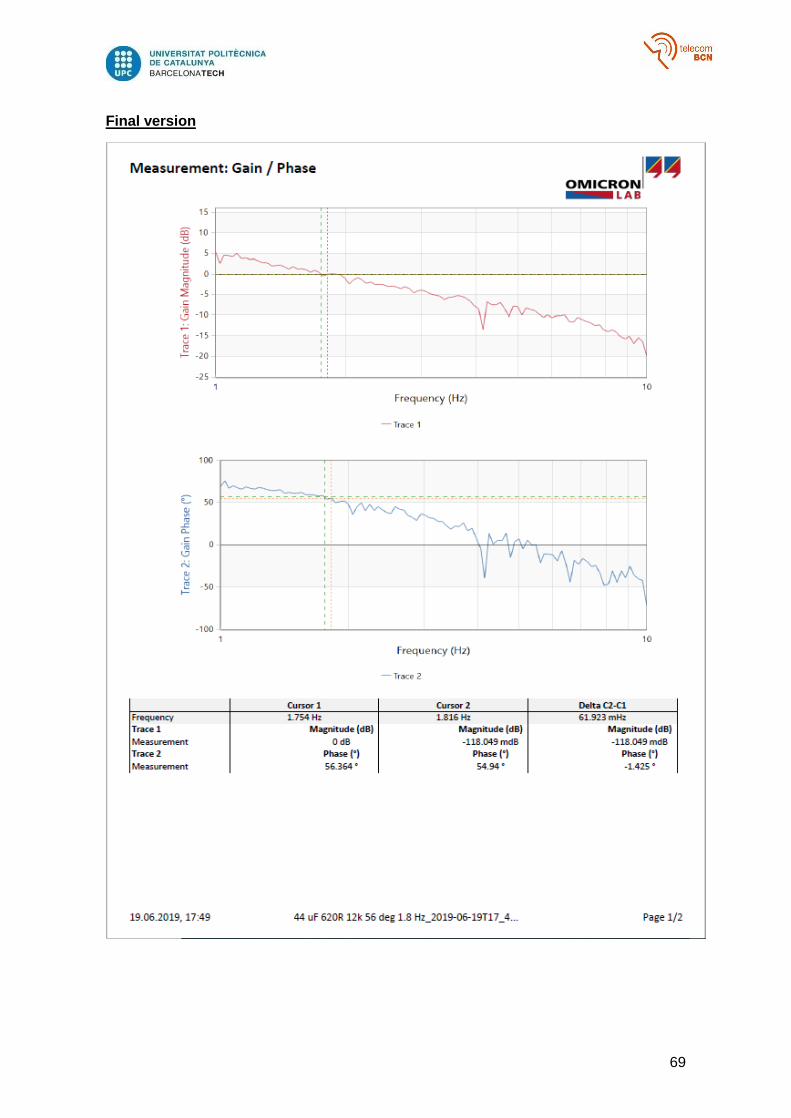
69
Final version
70
71
Glossary
ADC: Analog to Digital Converter
DAC: Digital to Analog Converter
EV: Electric Vehicle
IC: Integrated Circuit
ISR: Interrupt Service Routine
MOSFET: Metal-oxide-semiconductor Field-effect-transistor
Op Amp: Operational Amplifier
PIE: Peripheral Interrupt Expansion
PI: Proportional Integral
uC: Microcontroller
SCI: Serial Communications Interface
VCO: Voltage Controlled Oscillator
WPT: Wireless Power Transfer